Embed Size (px)
Citation preview

Panel Level Embedded Technology
System in a Package Global Summit 2013
Dr. Dyi-Chung HuSr. VP. Unimicron

DC Hu09062013
Outline
• Introduction to panel level embedded technology• Panel level embedded technology
– Line embedded– Passive components embedded– Active devices embedded– Many components Embedded
• Summary and conclusions

DC Hu09062013
Mobile Device Everywhere
�Everyone has mobile device(smart phone or tablet) and can use it everywhere.
�Everyone can be connected and interact with each other anytime anywhere.

DC Hu09062013
Mobile Applications Drive the Package Development
� System packaging needs �Small form factor
�High performance
�High bandwidth
�Low power consumption
�Low cost Small form factor
Lower CostHigh
Bandwidth
Lower power consumption

DC Hu09062013
WLP and PLP
Wafer Level Package (WLP)
Panel Level Package (PLP)
Processing Size 12” 20”or larger
Material Base Major is silicon, but glass and organic are possible
Major organic but glass or a-silicon are possible
Equipment Semiconductor centric;Stepper, coater, sputter..
Organic substrate centric;Laser via, e-less, lamination of dielectric..
Density Capabilities Down to 1 um L/S, via 5 um
Down to 5 um L/S, via 30 um
Cost down Potential Baseline Better
DC Hu09062013
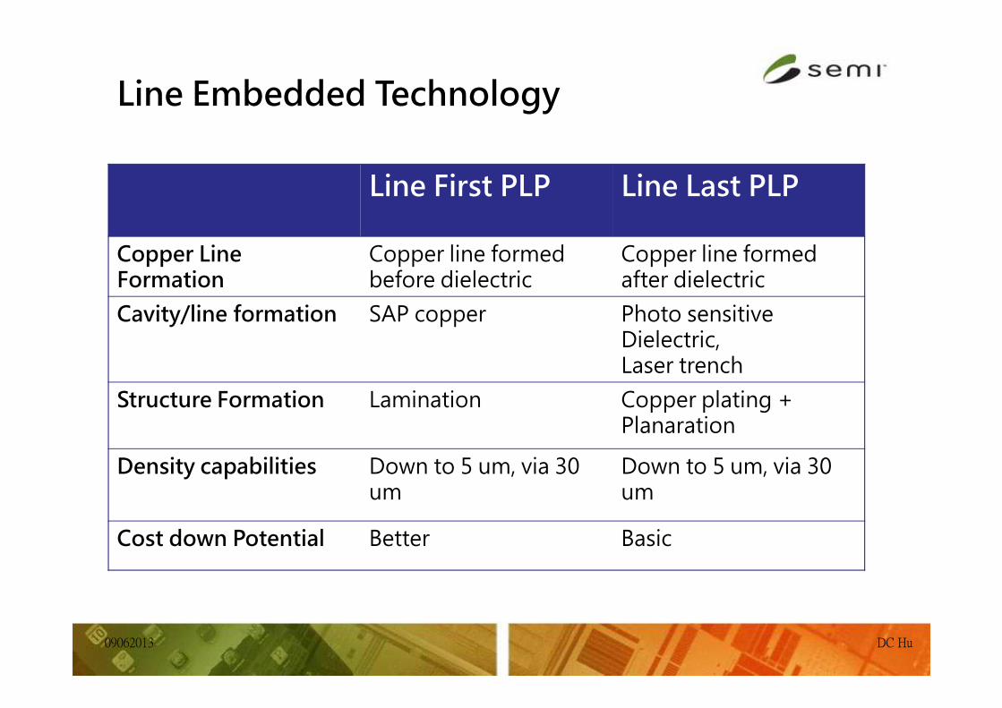
Line Embedded Technology
Line First PLP Line Last PLP
Copper Line Formation
Copper line formed before dielectric
Copper line formed after dielectric
Cavity/line formation SAP copper Photo sensitive Dielectric,Laser trench
Structure Formation Lamination Copper plating + Planaration
Density capabilities Down to 5 um, via 30 um
Down to 5 um, via 30 um
Cost down Potential Better Basic

DC Hu09062013
Line Last Embedded Technology
� Laser or photosensitive dielectric trench formation
� L/S < 8/8 um fine pitch trench can be formed
� Better adhesion than SAP process
� Challenges:
� Materials availability
� Copper line revealing process
10/10 um10/10 um10/10 um10/10 um8/8 um8/8 um8/8 um8/8 um6/6 um6/6 um6/6 um6/6 um
DC Hu09062013
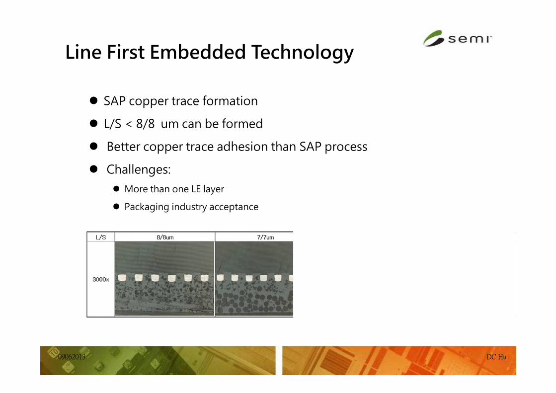
Line First Embedded Technology
� SAP copper trace formation
� L/S < 8/8 um can be formed
� Better copper trace adhesion than SAP process
� Challenges:
� More than one LE layer
� Packaging industry acceptance

DC Hu09062013
Prepreg
SR
SR
Embedded Trace Pattern
Total Thickness :130±30um
Unimicron UTS-EP (Ultra Thin Substrate – Embedded Pattern)
� Benefits:
� Z height reduction, low profile
� Better copper trace adhesion
� Good BOL assembly reliability
� Proven 15/15 um reliability
� Challenges
� Warpage control
� Packaging Industry acceptance

DC Hu09062013
Advantages of Embedded Passive/Active Substrate
� Form factor reduction
� Enhance electrical performance*
Normal Embedded
Packaging area reduction PoP thickness reduction
SMT MLCC Noise Embedded MLCC Noise reduction*
*: Murata
DC Hu09062013
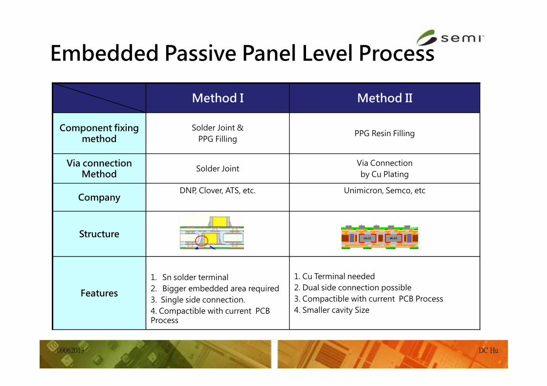
Embedded Passive Panel Level Process
Method I Method II
Component fixing method
Solder Joint & PPG Filling
PPG Resin Filling
Via connection Method
Solder JointVia Connection by Cu Plating
CompanyDNP, Clover, ATS, etc. Unimicron, Semco, etc
Structure
Features
1. Sn solder terminal 2. Bigger embedded area required3. Single side connection.4. Compactible with current PCB Process
1. Cu Terminal needed2. Dual side connection possible3. Compactible with current PCB Process 4. Smaller cavity Size

DC Hu09062013
Embedded Passive Substrate Process Key Items
� Components placement accuracy
� Interface Adhesion with Dielectric Layer
� Warpage Control
MLCCMLCCMLCCMLCC
MLCCMLCCMLCCMLCC MLCCMLCCMLCCMLCC

DC Hu09062013
MLCC Cross Section
MLCC Information:
Size: 0402
Thickness: 0.11mm
Capacitance: 100nF
Pitch between electrode:
2.0 um

DC Hu09062013
Embedded Component Substrate Process
ConfidentialConfidentialConfidentialConfidential
14
Through hole Drilling
Core Layer
Patterning
MLCC Embedding
Taping
MLCC Placement
Cavity Formation
Lamination side 1
Build upSolder Mask
Surface Finishing
MLCC
MLCC
MLCCLamination side
2
Strip Forming
Shipping

DC Hu09062013
Roadmap of Embedded Passive Substrate
2012 2013 2014 2015 2016
Year
Embedded Component M
LC
C
Res
isto
r
Ind
uct
or
Mu
lti-
Co
mp
on
ents
R C C RType
Size 0402 0201 01005
Discrete numbers per cavity
StructureDesign
Inner 2L;1/2/1 Coreless1/0/1
100um 60um W/O coreCore Thk.

DC Hu09062013
Comparison of Embedded Active & Passive Components
Active Passive
Embedded Component Size Large Small
Thickness < 100 um 100 um min.
I/Q Counts Many Few
Embedded Quantities One, Few Many
Material Base Silicon Ceramic/glass
Surface Base PI Ceramic/glass
Electrode Base Plated Cu Plated Cu
Component Package Wafer / Tray / Tape & Reel Tape & Reel
Placement Equipment Chip Shooter / Die Bonder Chip Shooter

DC Hu09062013
FOWLP and PLP Process Comparison
FOWLP PLP
Structure
Substrate Size ∆ O
Symmetrical Build No Yes*
L/S-Routing Density O ∆Thickness O ∆Equipment Cost ∆ O3D Extendibility O OCost Down Potential ∆ O
O: Good ; ∆:OK*: Single side possible

DC Hu09062013
Structure Roadmap of Embedded Active Substrate
PoP
Module
EmbeddedPackage
Multi-Chip Embedded Package
Dual Die
Active +Passive
PLP Package
FOWLP Package
FOWLP PoP
2012 2013 2014 2015 2016

DC Hu09062013
� Features:� Combine interposer and organic substrate.� Eliminates the solder joints between interposer and organic
substrate.
� Benefits:� Layer reduction compare with conventional organic substrate.� Alternative solution for high density SiP.� Cost reduction by interposer/carrier integration.
Embedded Interposer Carrier (EIC)
Interposer
Embedded Interposer Carrier (EIC)
Organic Laminated Substrate
D
IPD P
CAP

DC Hu09062013
ChipChip
Chip on Interposer on Substratevs. FC-EIC
� Chip on Interposer on Substrate: (CoIoS)� Interposer need double side RDL/Bumping and assembly process.� Four testing steps are used: Interposer, carrier, Interposer+carrier,� chip+interposer +carrier.
� FC-EIC: Flip Chip – Embedded Interposer Carrier� Interposer needs to be embedded into the substrate.� Only two testing steps are used: interposer, and interposer+carrier.
� Risk of thin wafer handling process is reduced..
CoIoS FC-EIC

DC Hu09062013
FC-EIC Benefits
� FC-EIC has low profile and cost benefit than ColoS.� This structure eliminates the solder joining between the interposer and
the laminated organic substrate.� The connections of interposer to carrier in EIC structure are copper to
copper which have less resistance and inductance compare to the conventional solder joints; better electrical performance.
� Know good EIC substrate, reduce chip assemble loss.� Interposer is protected by the carrier in EIC structure.� Large interposer sizes are possible.� Thin interposers (30 or 50 um thickness) can be included in
EIC structure. Thin interposers have a lower processing cost in via forming and via plating.
� EIC structure has a lower profile than CoIoS.� EIC structure is compatible with current backend
infrastructure.
DC Hu09062013
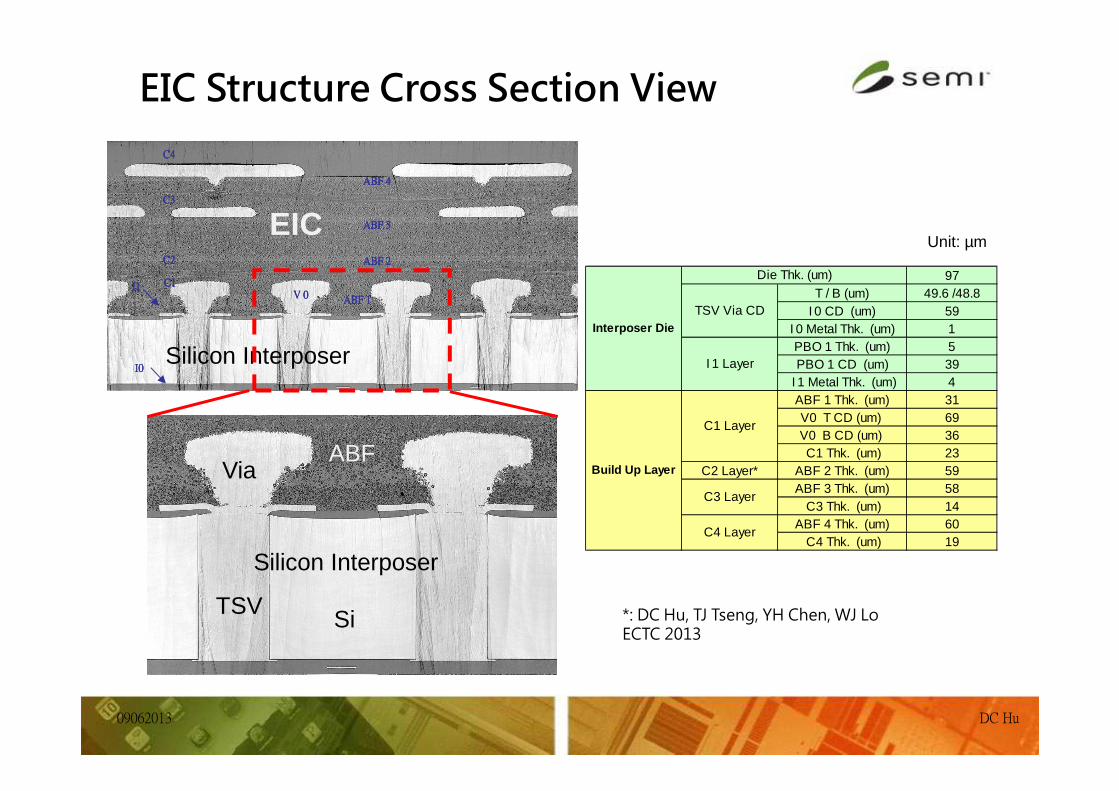
I0I0I0I0Silicon Interposer
I1I1I1I1V 0V 0V 0V 0
ABF ABF ABF ABF 2222
ABF 1 ABF 1 ABF 1 ABF 1
ABF ABF ABF ABF 3333
ABF ABF ABF ABF 4444
C1C1C1C1
C3C3C3C3
C4C4C4C4
C2C2C2C2
Via
97T / B (um) 49.6 /48.8
I 0 CD (um) 59I 0 Metal Thk. (um) 1PBO 1 Thk. (um) 5PBO 1 CD (um) 39
I 1 Metal Thk. (um) 4ABF 1 Thk. (um) 31V0 T CD (um) 69V0 B CD (um) 36 C1 Thk. (um) 23
C2 Layer* ABF 2 Thk. (um) 59ABF 3 Thk. (um) 58
C3 Thk. (um) 14ABF 4 Thk. (um) 60
C4 Thk. (um) 19C4 Layer
Interposer Die
Build Up Layer
Die Thk. (um)
I 1 Layer
C1 Layer
C3 Layer
TSV Via CD
Unit: µm
EIC Structure Cross Section View
EIC
Silicon Interposer
*: DC Hu, TJ Tseng, YH Chen, WJ LoECTC 2013
ABF
TSV Si

DC Hu09062013
The Changing Role of Substrate
New Role of Substrate in 3D ERA
- Panel Level Module Integration -
Now Future
Optical Fiber

DC Hu09062013
Summary and Conclusions
1. Panel level embedded technology is becoming a fast growing technology to achieve the packaging requirement of; small form factor, high performance and low cost.
2. Currently embedded passive components is in mass production, and embeding active device is emerging.
3. Panel Level Packing has potential cost advantage over FOWLP due to her PCB centric production infrastructure.
4. Equipment and material improvement will expend the scope of panel level embedded technology.
5. New concept such as embedded interposer or other components into the substrate is emerging.
6. The role of laminate substrate is emerging as a system integrator based on panel level embedding technology.

DC Hu09062013
Thank you for your Attention!


![SEMI CAST TEMS Overview 2017Mayprod7.semi.org/en/sites/semi.org/files/data17/docs... · 7(06 0hvvdjh 7\shv 0hvvdjh 1dph 0hvvdjh 1dph &rpphqw 7&6 ,qlwldol]dwlrq 7&6 6kxwgrzq 6\vwhp](https://img.dokumen.tips/doc/110x75/5e7c1dbaa1720b189f44faf7/semi-cast-tems-overview-706-0hvvdjh-7shv-0hvvdjh-1dph-0hvvdjh-1dph-rpphqw.jpg)