Embed Size (px)
Citation preview
PAN9026 Wi-Fi Dual Band 2.4/5 GHz and Bluetooth Module
Design Guide
Rev. 1.0
Wireless Modules
PAN9026 Design Guide
Design Guide 1.0 Page 2
Overview
The PAN9026 is a 2.4/5 GHz ISM band Wi Fi and
Bluetooth radio module, which includes a wireless
radio for easy integration of Wi Fi and Bluetooth
connectivity into various electronic devices.
Features
• Dual band 2.4/5 GHz 802.11 a/b/g/n Wi-Fi/BT combo module
• Supports 802.11i security standards through AES, CCMP, and more security mechanisms
• 802.11e Quality of Service is supported for multimedia applications
• IEEE 802.11n-compliant, 1x1 spatial stream with data rates up to MCS7 150 Mbps
• Bluetooth 5.0 (includes LE)
• Dual simultaneous and independent WLAN and Bluetooth operation
• Dynamic Rapid Channel Switching (DRCS) for simultaneous operation in 2.4 GHz and 5 GHz bands
• Indoor Location and Navigation with IEEE 802.11mc
• Power management with sleep clock
• Coexistence interface for arbitration of co-located WLAN, Bluetooth, or Mobile Wireless System (e.g. LTE)
• Generic interfaces include SDIO 3.0 and high-speed UART for host processor connection
• Software Linux driver
Characteristics
• Surface Mount Type (SMT) 17.5 mm x 10.0 mm x 2.6 mm
• Marvell® 88W8977 WLAN 2.4/5 GHz and Bluetooth single-chip solution inside
• TX Power +16 dBm @ 802.11b
• RX Sensitivity -98 dBm @ 802.11b DSSS 1 Mbps
• IEEE 802.11n 20 MHz and 40 MHz channel bandwidth
• Long and Short Guard Interval support
• Power supply 3.3 V, 2.2 V, 1.8 V
• Current consumption Wi-Fi typical 400 mA @ TX and 70 mA @ RX
• SDIO 1-bit or 4-bit
• Wide temperature range of -30 to +85 °C
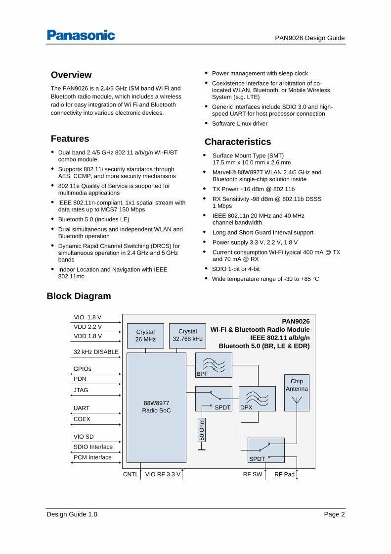
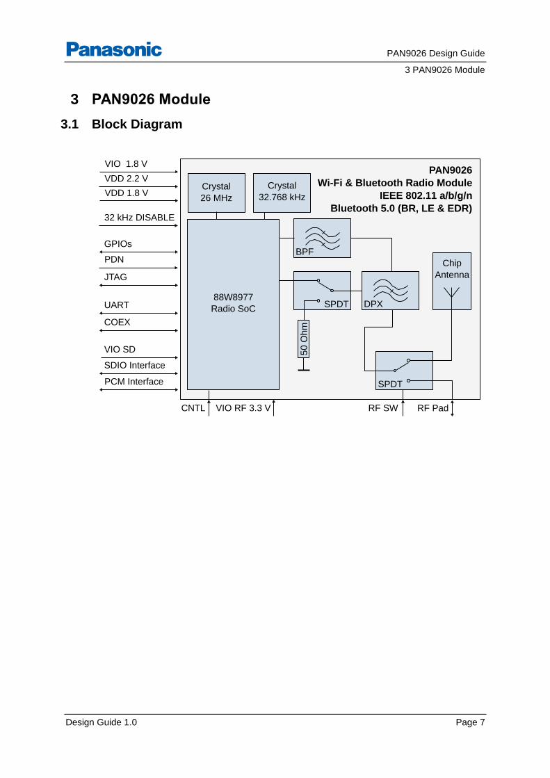
Block Diagram
Chip
Antenna
SPDT
88W8977
Radio SoC
Crystal
32.768 kHz
SPI
UART
COEX
GPIOs
Status LED's
MCU Ready
PDN
Factory Reset
V SPDT
Wake Up's
JTAG
VIO 1.8 V
BPF
RF Pad
PAN9026
Wi-Fi & Bluetooth Radio Module
IEEE 802.11 a/b/g/n
Bluetooth 5.0 (BR, LE & EDR)
Crystal
26 MHz
DPXSPDT
50 O
hm
VDD 2.2 V
VDD 1.8 V
PCM Interface
SDIO Interface
VIO SD
32 kHz DISABLE
RF SWVIO RF 3.3 VCNTL
PAN9026 Design Guide
Design Guide 1.0 Page 3
By purchase of any of the products described in this document the customer accepts the document's
validity and declares their agreement and understanding of its contents and recommendations. Panasonic
Industrial Devices Europe GmbH (Panasonic) reserves the right to make changes as required at any time
without notification. Please consult the most recently issued Design Guide before initiating or completing a
design.
© Panasonic Industrial Devices Europe GmbH 2017.
This specification sheet is copyrighted. Reproduction of this document is permissible only if reproduction is
without alteration and is accompanied by all associated warranties, conditions, limitations, and notices. Do
not disclose it to a third party.
All rights reserved.
This Design Guide does not lodge the claim to be complete and free of mistakes.
Engineering Samples (ES)
If Engineering Samples are delivered to the customer, these samples have the status “Engineering
Samples”. This means that the design of this product is not yet concluded. Engineering Samples may be
partially or fully functional, and they may differ from the published Product Specification.
Engineering Samples are not qualified and they are not to be used for reliability testing or series
production.
Disclaimer
The customer acknowledges that samples may deviate from the Design Guide and may bear defects due
to their status of development and the lack of qualification mentioned above.
Panasonic rejects any liability or product warranty for Engineering Samples. In particular, Panasonic
disclaims liability for damages caused by:
The use of the Engineering Sample other than for evaluation purposes, particularly the installation
or integration in another product to be sold by the customer,
Deviation or lapse in function of the Engineering Sample,
Improper use of the Engineering Sample.
Panasonic Industrial Devices Europe GmbH disclaims any liability for consequential and incidental
damages. In case of any queries regarding the Engineering Samples, please contact your local sales
partner or the related product manager.
PAN9026 Design Guide
Design Guide 1.0 Page 4
Table of Contents
1 About This Document ......................................................................................................................... 5
1.1 Purpose and Audience .............................................................................................................. 5
1.2 Revision History ......................................................................................................................... 5
1.3 Use of Symbols ......................................................................................................................... 5
1.4 Related Documents ................................................................................................................... 5
2 Overview .............................................................................................................................................. 6
3 PAN9026 Module ................................................................................................................................. 7
3.1 Block Diagram ........................................................................................................................... 7
3.2 Footprint .................................................................................................................................... 8
3.3 Land Pattern .............................................................................................................................. 8
3.4 Solder Mask ............................................................................................................................... 9
3.5 Placement ................................................................................................................................ 10
3.6 Power Supply .......................................................................................................................... 12
3.7 RF Path ................................................................................................................................... 14
4 PAN9026 SDIO Adapter .................................................................................................................... 16
4.1 Live View ................................................................................................................................. 16
4.2 Functional Blocks .................................................................................................................... 17
4.3 Part Placement ........................................................................................................................ 18
4.4 Schematic ................................................................................................................................ 19
4.5 PCB Layout ............................................................................................................................. 20
5 Cautions ............................................................................................................................................ 24
5.1 Life Support Policy ................................................................................................................... 24
6 Appendix ........................................................................................................................................... 25
6.1 Ordering Information ................................................................................................................ 25
6.2 Contact Details ........................................................................................................................ 26
PAN9026 Design Guide
1 About This Document
Design Guide 1.0 Page 5
1 About This Document
1.1 Purpose and Audience
This Design Guide provides details on the electrical integration of the Panasonic PAN9026
module. It is intended for hardware design, application, and Original Equipment Manufacturers
(OEM) engineers. The product is referred to as “the PAN9026” or “the module” within this
document.
1.2 Revision History
Revision Date Modifications/Remarks
1.0 18.12.2017 First design guide version.
1.3 Use of Symbols
Symbol Description
Note
Indicates important information for the proper use of the product.
Non-observance can lead to errors.
Attention
Indicates important notes that, if not observed, can put the product’s functionality
at risk.
Tip
Indicates useful information designed to facilitate working with the PAN9026.
[chapter number]
[chapter title]
Cross reference
Indicates cross references within the document.
Example:
Description of the symbols used in this document 1.3 Use of Symbols.
Requirement
Indicates a requirement that must be met before the corresponding tasks can be
completed.
1.4 Related Documents
Please refer to the Panasonic website for related documents 6.2.2 Product Information.
PAN9026 Design Guide
2 Overview
Design Guide 1.0 Page 6
2 Overview
This Design Guide applies to the PAN9026 WLAN/BT combo module and the PAN9026 SDIO
Adapter development platform. The intention is to enable our customers to easily and fast
integrate our module PAN9026 in their product. This Design Guide describes the hardware
integration and gives useful hints.
This document is structured into two main parts:
• The hardware integration of the PAN9026 module.
• The PAN9026 SDIO Adapter as an example for the module integration.
Please refer to the Panasonic website for related documents 6.2.2 Product Information.
Further information on the variants and versions 6.1 Ordering Information.
PAN9026 Design Guide
3 PAN9026 Module
Design Guide 1.0 Page 7
3 PAN9026 Module
3.1 Block Diagram
Chip
Antenna
SPDT
88W8977
Radio SoC
Crystal
32.768 kHz
SPI
UART
COEX
GPIOs
Status LED's
MCU Ready
PDN
Factory Reset
V SPDT
Wake Up's
JTAG
VIO 1.8 V
BPF
RF Pad
PAN9026
Wi-Fi & Bluetooth Radio Module
IEEE 802.11 a/b/g/n
Bluetooth 5.0 (BR, LE & EDR)
Crystal
26 MHz
DPXSPDT5
0 O
hm
VDD 2.2 V
VDD 1.8 V
PCM Interface
SDIO Interface
VIO SD
32 kHz DISABLE
RF SWVIO RF 3.3 VCNTL
PAN9026 Design Guide
3 PAN9026 Module
Design Guide 1.0 Page 8
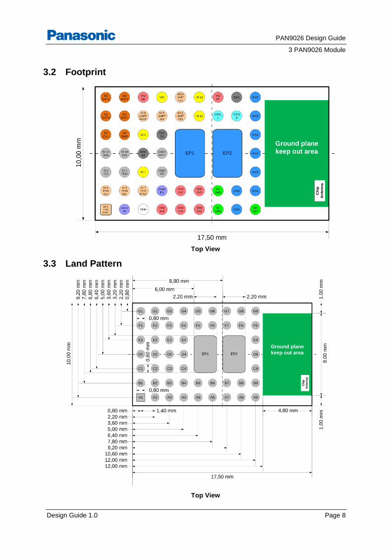
3.2 Footprint
Top View
3.3 Land Pattern
Top View
PAN9026 Design Guide
3 PAN9026 Module
Design Guide 1.0 Page 9
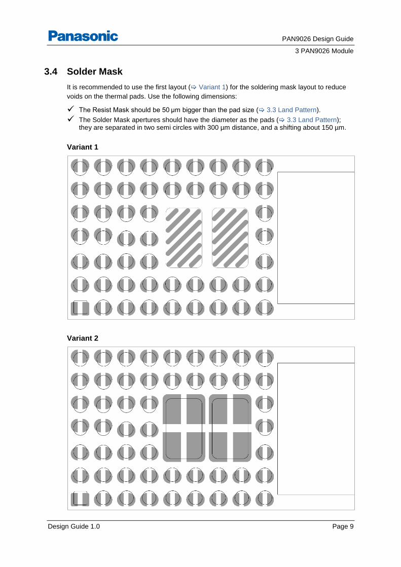
3.4 Solder Mask
It is recommended to use the first layout ( Variant 1) for the soldering mask layout to reduce
voids on the thermal pads. Use the following dimensions:
The Resist Mask should be 50 µm bigger than the pad size ( 3.3 Land Pattern).
The Solder Mask apertures should have the diameter as the pads ( 3.3 Land Pattern); they are separated in two semi circles with 300 µm distance, and a shifting about 150 µm.
Variant 1
Variant 2

PAN9026 Design Guide
3 PAN9026 Module
Design Guide 1.0 Page 10
3.5 Placement
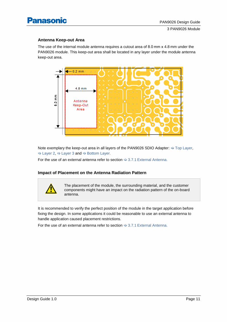
Antenna Keep-out Area
Do not place any ground plane under the marked restricted antenna area in any layer! This would be affecting the performance of the chip antenna in a critical manner.
Further information Antenna Keep-out Area.
The following conditions must be met:
Keep this product away from heat. Heat is the major cause of decreasing the life of these products.
Keep this product away from other high frequency circuits.
Dimensions are in mm.
Note: The above recommendation for the ground plane is based on a FR4 4-Layer PCB.
Min. 15 mm Min. 15 mm10 mm
PAN9026
Out line
Top View
17
.5 m
m
Min
. 4
0 m
m
Use a ground plane in
the area surrounding the
PAN9026 module wherever
possible.
Pla
ce
PA
N9
02
6 a
t th
e
ed
ge
of
the
mo
the
r P
CB
.
If possible place PAN9026 in
the center of mother PCB.
Rest ricted Area
No copper on
any layer
PAN9026 Design Guide
3 PAN9026 Module
Design Guide 1.0 Page 11
Antenna Keep-out Area
The use of the internal module antenna requires a cutout area of 8.0 mm x 4.8 mm under the
PAN9026 module. This keep-out area shall be located in any layer under the module antenna
keep-out area.
Note exemplary the keep-out area in all layers of the PAN9026 SDIO Adapter: Top Layer,
Layer 2, Layer 3 and Bottom Layer.
For the use of an external antenna refer to section 3.7.1 External Antenna.
Impact of Placement on the Antenna Radiation Pattern
The placement of the module, the surrounding material, and the customer components might have an impact on the radiation pattern of the on-board antenna.
It is recommended to verify the perfect position of the module in the target application before
fixing the design. In some applications it could be reasonable to use an external antenna to
handle application caused placement restrictions.
For the use of an external antenna refer to section 3.7.1 External Antenna.
PAN9026 Design Guide
3 PAN9026 Module
Design Guide 1.0 Page 12
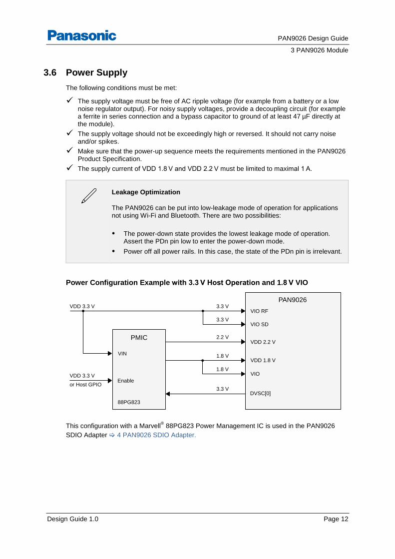
3.6 Power Supply
The following conditions must be met:
The supply voltage must be free of AC ripple voltage (for example from a battery or a low noise regulator output). For noisy supply voltages, provide a decoupling circuit (for example a ferrite in series connection and a bypass capacitor to ground of at least 47 µF directly at the module).
The supply voltage should not be exceedingly high or reversed. It should not carry noise and/or spikes.
Make sure that the power-up sequence meets the requirements mentioned in the PAN9026 Product Specification.
The supply current of VDD 1.8 V and VDD 2.2 V must be limited to maximal 1 A.
Leakage Optimization
The PAN9026 can be put into low-leakage mode of operation for applications not using Wi-Fi and Bluetooth. There are two possibilities:
• The power-down state provides the lowest leakage mode of operation. Assert the PDn pin low to enter the power-down mode.
• Power off all power rails. In this case, the state of the PDn pin is irrelevant.
Power Configuration Example with 3.3 V Host Operation and 1.8 V VIO
This configuration with a Marvell® 88PG823 Power Management IC is used in the PAN9026
SDIO Adapter 4 PAN9026 SDIO Adapter.
PAN9026
VIO SD
VIO RF
VDD 2.2 V
VDD 1.8 V
DVSC[0]
88PG823
PMIC
Enable
VDD 3.3 V 3.3 V
3.3 V
2.2 V
1.8 V
3.3 V
VDD 3.3 V
or Host GPIO
VIN
1.8 VVIO
PAN9026 Design Guide
3 PAN9026 Module
Design Guide 1.0 Page 13
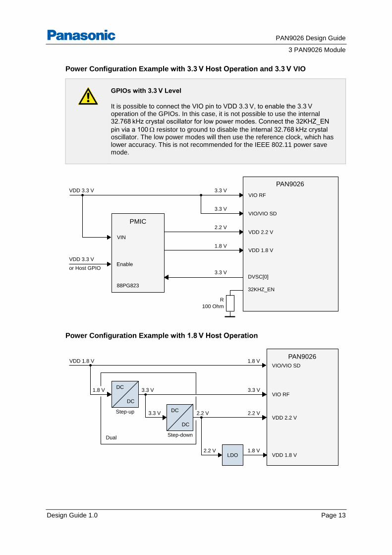
Power Configuration Example with 3.3 V Host Operation and 3.3 V VIO
GPIOs with 3.3 V Level
It is possible to connect the VIO pin to VDD 3.3 V, to enable the 3.3 V operation of the GPIOs. In this case, it is not possible to use the internal 32.768 kHz crystal oscillator for low power modes. Connect the 32KHZ_EN
pin via a 100 resistor to ground to disable the internal 32.768 kHz crystal oscillator. The low power modes will then use the reference clock, which has lower accuracy. This is not recommended for the IEEE 802.11 power save mode.
Power Configuration Example with 1.8 V Host Operation
PAN9026
VIO/VIO SD
VIO RF
VDD 2.2 V
VDD 1.8 V
DVSC[0]
88PG823
PMIC
Enable
VDD 3.3 V 3.3 V
3.3 V
2.2 V
1.8 V
3.3 V
VDD 3.3 V
or Host GPIO
VIN
R
100 Ohm
32KHZ_EN
PAN9026
VIO/VIO SD
VIO RF
VDD 2.2 V
VDD 1.8 V
3.3 V
2.2 V
1.8 V
DC
DC
DC
DC
LDO
Step-up
Step-down
VDD 1.8 V 1.8 V
1.8 V
3.3 V
3.3 V
2.2 V
2.2 V
Dual
PAN9026 Design Guide
3 PAN9026 Module
Design Guide 1.0 Page 14
Power-up Sequence
The power-up sequence must meet the requirements mentioned in the chapter Power-up Sequence in the PAN9026 Product Specification.
3.7 RF Path
3.7.1 External Antenna
Antenna Warning
The PAN9026 is tested with a standard U.FL connector and with the antenna listed in the regulatory and certification chapter of the PAN9026 Product Specification. When integrated into the OEM’s product, these fixed antennas require installation preventing end users from replacing them with non-approved antennas. Any antenna not in the regulatory and certification chapter of the PAN9026 Product Specification must be tested to comply with FCC Section 15.203 for unique antenna connectors and with Section 15.247 for emissions.
The PAN9026 module has a 50 RF pin (SMD pad). Connect an external antenna directly or
via a connector (e.g. U.FL) with RF trace to this RF pin. This RF trace shall be matched to 50
3.7.2 RF Trace.
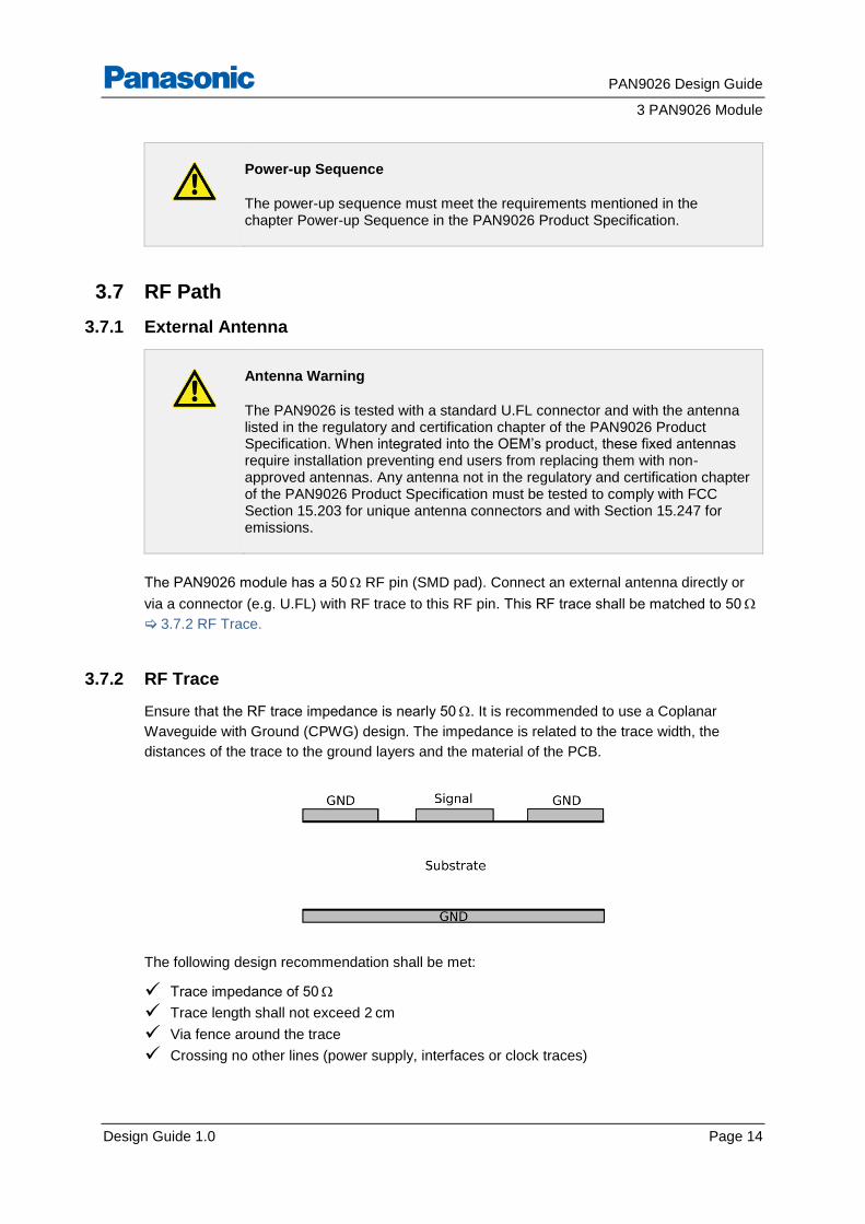
3.7.2 RF Trace
Ensure that the RF trace impedance is nearly 50 . It is recommended to use a Coplanar
Waveguide with Ground (CPWG) design. The impedance is related to the trace width, the
distances of the trace to the ground layers and the material of the PCB.
The following design recommendation shall be met:
Trace impedance of 50
Trace length shall not exceed 2 cm
Via fence around the trace
Crossing no other lines (power supply, interfaces or clock traces)
PAN9026 Design Guide
3 PAN9026 Module
Design Guide 1.0 Page 15
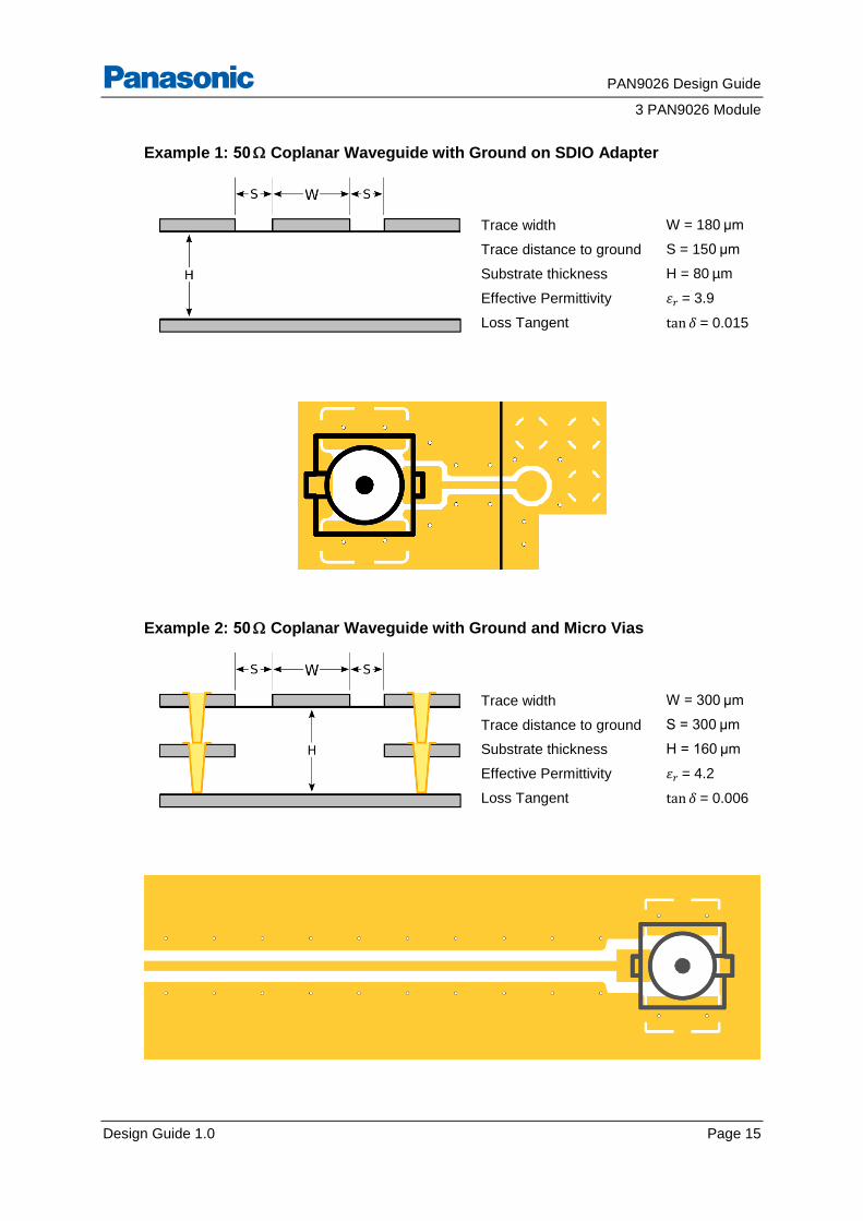
Example 1: 50 Coplanar Waveguide with Ground on SDIO Adapter
Trace width
Trace distance to ground
Substrate thickness
Effective Permittivity
Loss Tangent
W = 180 µm
S = 150 µm
H = 80 µm
휀𝑟 = 3.9
tan 𝛿 = 0.015
Example 2: 50 Coplanar Waveguide with Ground and Micro Vias
Trace width
Trace distance to ground
Substrate thickness
Effective Permittivity
Loss Tangent
W = 300 µm
S = 300 µm
H = 160 µm
휀𝑟 = 4.2
tan 𝛿 = 0.006
PAN9026 Design Guide
4 PAN9026 SDIO Adapter
Design Guide 1.0 Page 16
4 PAN9026 SDIO Adapter
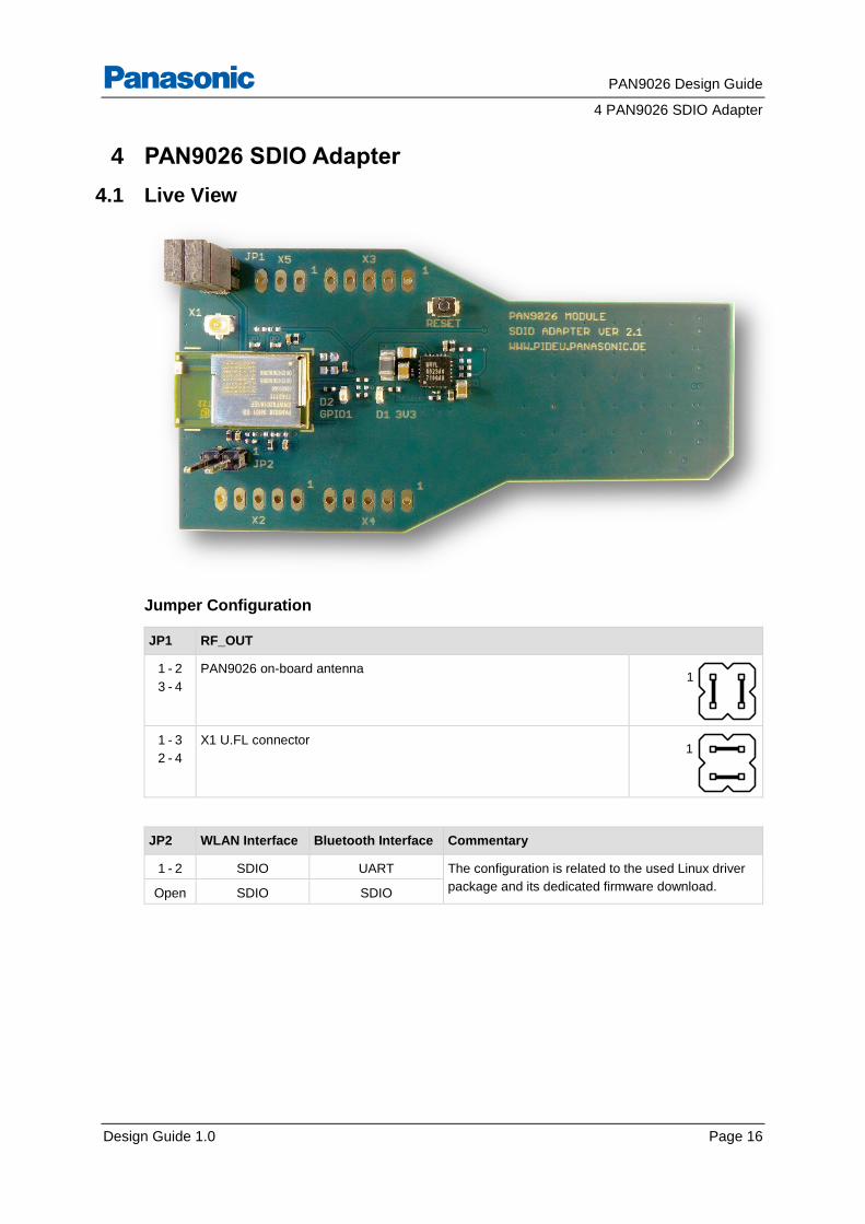
4.1 Live View
Jumper Configuration
JP1 RF_OUT
1 - 2
3 - 4
PAN9026 on-board antenna
1 - 3
2 - 4
X1 U.FL connector
JP2 WLAN Interface Bluetooth Interface Commentary
1 - 2 SDIO UART The configuration is related to the used Linux driver
package and its dedicated firmware download. Open SDIO SDIO
1
1
PAN9026 Design Guide
4 PAN9026 SDIO Adapter
Design Guide 1.0 Page 17
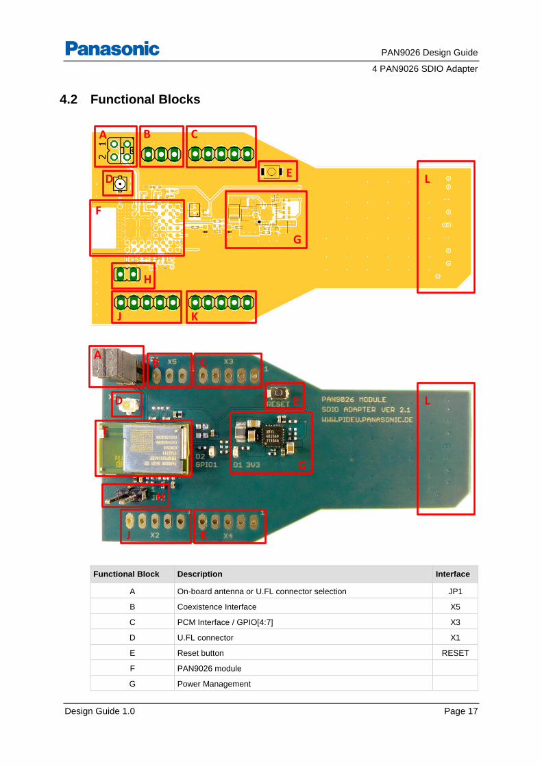
4.2 Functional Blocks
Functional Block Description Interface
A On-board antenna or U.FL connector selection JP1
B Coexistence Interface X5
C PCM Interface / GPIO[4:7] X3
D U.FL connector X1
E Reset button RESET
F PAN9026 module
G Power Management
D
F
G
E L
A B C
J K
H
F
D
A B C
E
G
H
J K
L

PAN9026 Design Guide
4 PAN9026 SDIO Adapter
Design Guide 1.0 Page 18
Functional Block Description Interface
H WLAN / Bluetooth Interface configuration (CNTL0) JP2
J GPIO Interface / GPIO[0:1,12:13] X2
K UART HCI Interface / GPIO[8:11] X4
L SDIO Interface (VIO SD 3.3V)
4.3 Part Placement
X2
X4
JP2
R8 C14
R16 R17 MOD1
R19 C11
C6
R18
X1
JP1
X5
X3
C12
R11 C13
R10
C10 R9
Z1
C7
R13 R14
R15
R7
ED2
ED1
R6
L1
C9 C2 C5
IC1 R3 C4
C1
C8 R5
R12 R4
R2
R1
C3 S1
PAN9026 Design Guide
4 PAN9026 SDIO Adapter
Design Guide 1.0 Page 19
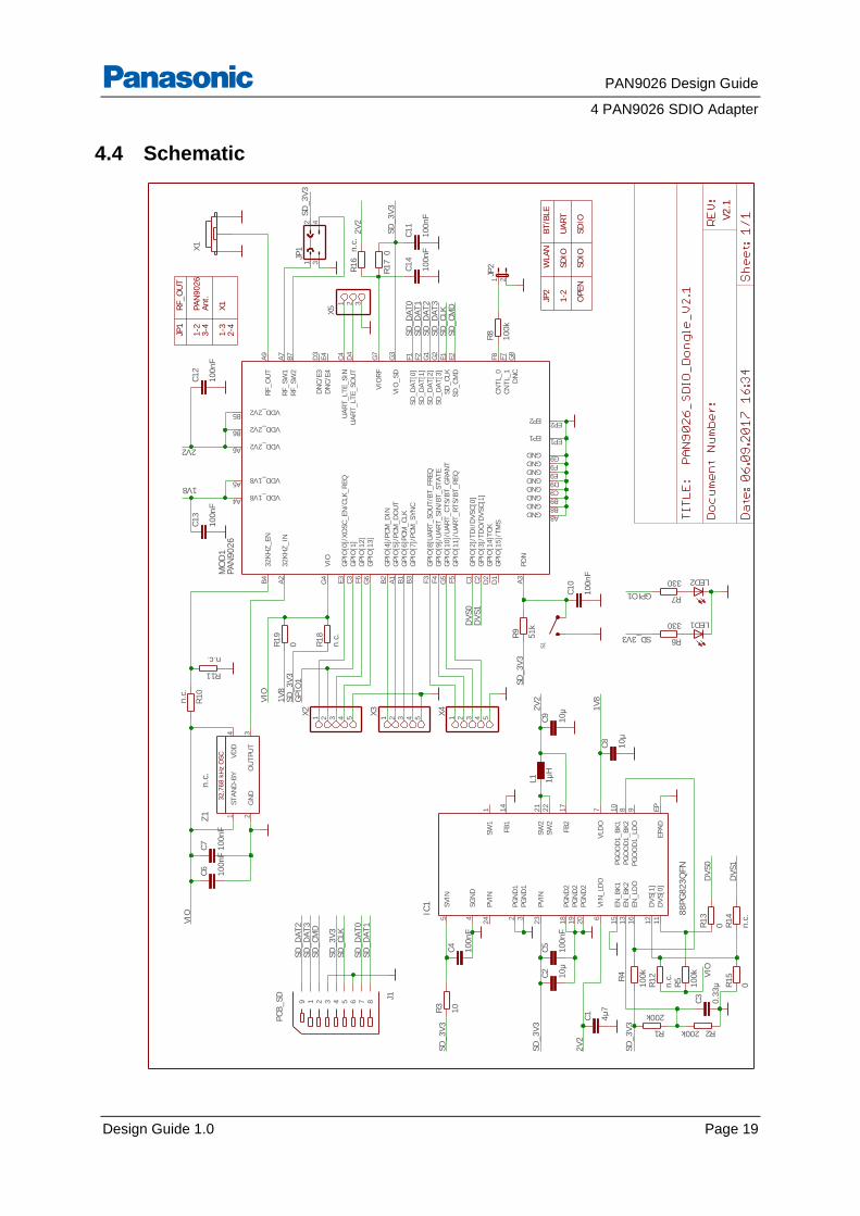
4.4 Schematic
330
10µ
100nF
100nF
330
100k
0.3
3µ
PC
B_SD
PA
N9026
88PG
823Q
FN
100k
200k
200k
10
100nF
4µ
7
10µ
10µ
1µ
H
100nF
100nF
100nF
100k
51k
100nF
100nF
100nF
n.c
.
n.c.
n.c
.
0 n.c
.0
n.c
.
0
n.c
.
0
X1
S1
LED2
R7
LED1
C2
C4
C10
R6
R5
C3
X2
1 2 3 4 5
J1
1 2 3 4 5 6 7 89
MO
D1
GPIO
[1]
C3
GPIO
[2]/
TD
I/D
VS
C[0
]C
1
GPIO
[3]/
TD
O/D
VS
C[1
]C
2
GPIO
[4]/
PC
M_D
INB
2
GPIO
[0]/
XO
SC
_E
N/C
LK
_R
EQ
E3
GPIO
[5]/
PC
M_D
OU
TA
1
GPIO
[6]P
CM
_C
LK
B1
GPIO
[7]/
PC
M_S
YN
CB
3
GPIO
[8]U
AR
T_S
OU
T/B
T_FR
EQ
F3
GPIO
[9]/
UA
RT
_S
IN/B
T_S
TA
TE
F4
GPIO
[10]/
UA
RT
_C
TS
/BT
_G
RA
NT
G5
GPIO
[11]/
UA
RT
_R
TS
/BT
_R
EQ
F5
GPIO
[12]
F6
GPIO
[13]
G6
GPIO
[14]T
CK
D2
GPIO
[15]/
TM
SD
1
DN
C/E
3D
3
DN
C/E
4E
4
UA
RT
_LT
E_S
INC
4
UA
RT
_LT
E_S
OU
TD
4
SD
_C
MD
E2
SD
_C
LK
E1
SD
_D
AT
[3]
G2
SD
_D
AT
[2]
G1
SD
_D
AT
[1]
F2
SD
_D
AT
[0]
F1
PD
NA
3
GNDA8
GNDB8
GNDB9
GNDC9
GNDD9
GNDE9
GNDF9
GNDG9
EP1EP1
EP2EP2
VDD_1V8A4
VDD_1V8A5
VDD_2V2A6
VDD_2V2B6
VIO
G4
VIO
_S
DG
3
32K
HZ
_E
NB
4
32K
HZ
_IN
A2
VDD_2V2B5
CN
TL_0
F8
CN
TL_1
F7
DN
CG
8
VIO
RF
G7
RF_O
UT
A9
RF_S
W1
A7
RF_S
W2
B7
Z1
n.c
.
ST
AN
D-B
Y1
GN
D2
OU
TPU
T3
VD
D4
X3
1 2 3 4 5
X4
1 2 3 4 5
IC1 SV
IN5
SG
ND
4
PV
IN24
PG
ND
12
PG
ND
13
PV
IN23
PG
ND
218
PG
ND
219
PG
ND
220
VIN
_LD
O6
EN
_B
K2
13
EN
_B
K1
15
EN
_LD
O16
DV
S[1
]12
DV
S[0
]11
EPA
DE
P
PG
OO
D1_LD
O9
PG
OO
D1_B
K2
8PG
OO
D1_B
K1
10
VLD
O7
FB
217
SW
222
SW
221
FB
114
SW
11
R4
R1 R2
R3
C5
C1
C9
C8
L1
C11
C6
C7
JP1
12
34
R8
R9
C12
C13
C14
JP2
1 2
X5
1 2 3
R10
R11
R12
R13
R14
R15
R16
R17
R18
R19
SD
_D
AT
2
SD
_D
AT
2
SD
_D
AT
3
SD
_D
AT
3
SD
_C
MD
SD
_C
MD
SD
_3V
3
SD
_3V
3
SD
_3V
3
SD
_3V
3
SD
_3V
3
SD_3V3
SD
_3V
3
SD
_3V
3
SD
_3V
3
SD
_D
AT
0
SD
_D
AT
0
SD
_D
AT
1
SD
_D
AT
1
SD
_C
LK
SD
_C
LK
GPIO
1
GPIO1
2V2
2V
2
2V
2
2V
2
1V8
1V
81V
8
DV
S0
DV
S0
DV
S1
DV
S1
VIO
VIO
VIO
V2.1
JP1
RF_O
UT
1-2
3-4
1-3
2-4
PA
N9026
Ant.
X1 JP
2W
LA
NB
T/B
LE
1-2
OPE
N
SD
IO
SD
IOSD
IO
UA
RT
32,7
68 k
Hz
OS
C
PAN9026 Design Guide
4 PAN9026 SDIO Adapter
Design Guide 1.0 Page 20
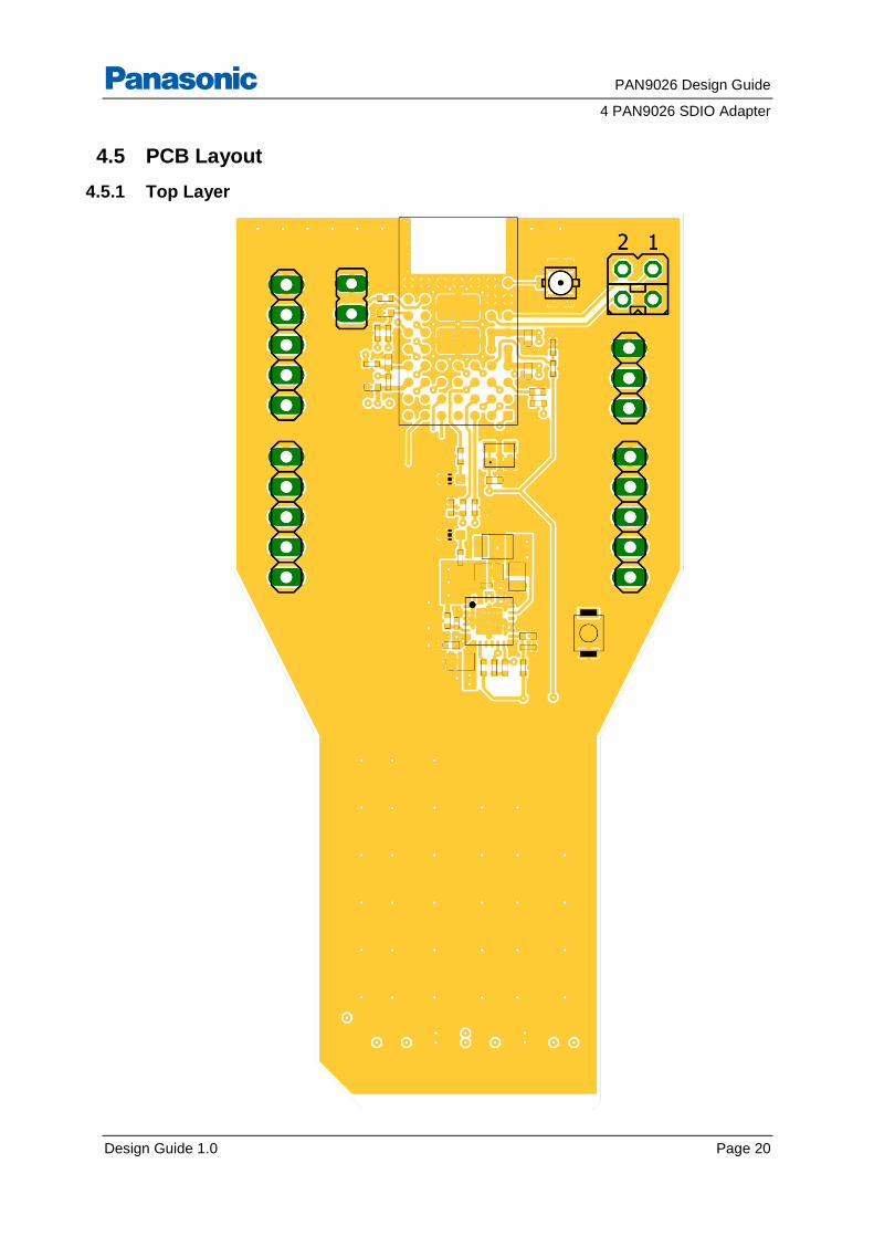
4.5 PCB Layout
4.5.1 Top Layer
PAN9026 Design Guide
4 PAN9026 SDIO Adapter
Design Guide 1.0 Page 21
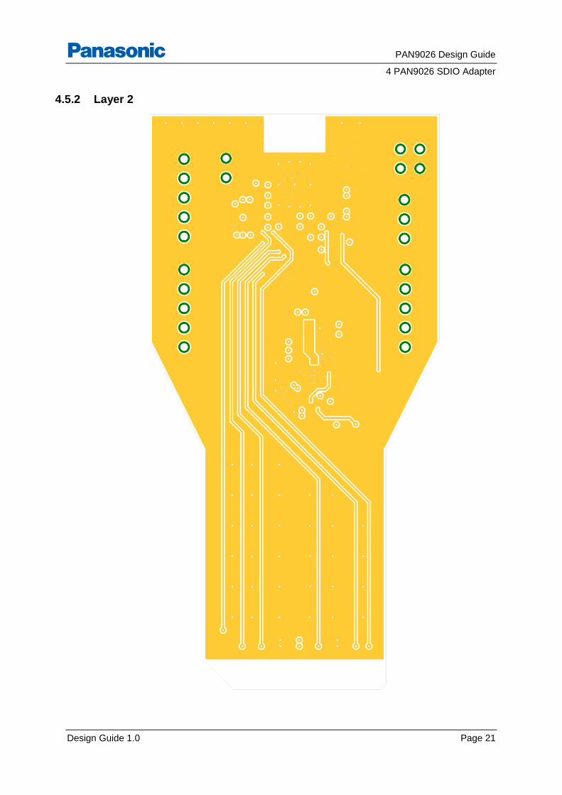
4.5.2 Layer 2
PAN9026 Design Guide
4 PAN9026 SDIO Adapter
Design Guide 1.0 Page 22
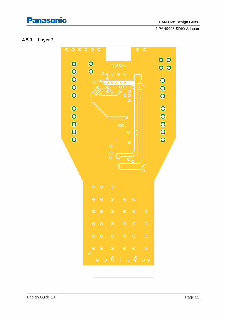
4.5.3 Layer 3
PAN9026 Design Guide
4 PAN9026 SDIO Adapter
Design Guide 1.0 Page 23
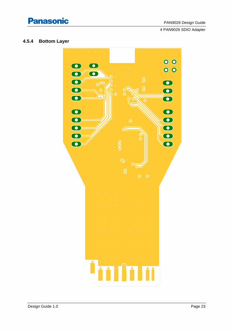
4.5.4 Bottom Layer
PAN9026 Design Guide
5 Cautions
Design Guide 1.0 Page 24
5 Cautions
5.1 Life Support Policy
This Panasonic Industrial Devices Europe GmbH product is not designed for use in life support
appliances, devices, or systems where malfunction can reasonably be expected to result in a
significant personal injury to the user, or as a critical component in any life support device or
system whose failure to perform can be reasonably expected to cause the failure of the life
support device or system, or to affect its safety or effectiveness.
Panasonic customers using or selling these products for use in such applications do so at their
own risk and agree to fully indemnify Panasonic Industrial Devices Europe GmbH for any
damages resulting.
PAN9026 Design Guide
6 Appendix
Design Guide 1.0 Page 25
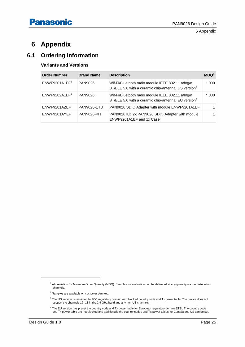
6 Appendix
6.1 Ordering Information
Variants and Versions
Order Number Brand Name Description MOQ1
ENWF9201A1EF2 PAN9026 Wif-Fi/Bluetooth radio module IEEE 802.11 a/b/g/n
BT/BLE 5.0 with a ceramic chip-antenna, US version3
1 000
ENWF9202A1EF2 PAN9026 Wif-Fi/Bluetooth radio module IEEE 802.11 a/b/g/n
BT/BLE 5.0 with a ceramic chip-antenna, EU version4
1 000
ENWF9201AZEF PAN9026-ETU PAN9026 SDIO Adapter with module ENWF9201A1EF 1
ENWF9201AYEF PAN9026-KIT PAN9026 Kit: 2x PAN9026 SDIO Adapter with module
ENWF9201A1EF and 1x Case
1
1 Abbreviation for Minimum Order Quantity (MOQ). Samples for evaluation can be delivered at any quantity via the distribution channels.
2 Samples are available on customer demand.
3 The US version is restricted to FCC regulatory domain with blocked country code and Tx power table. The device does not support the channels 12 -13 in the 2.4 GHz band and any non-US channels.
4 The EU version has preset the country code and Tx power table for European regulatory domain ETSI. The country code and Tx power table are not blocked and additionally the country codes and Tx power tables for Canada and US can be set.
PAN9026 Design Guide
6 Appendix
Design Guide 1.0 Page 26
6.2 Contact Details
6.2.1 Contact Us
Please contact your local Panasonic Sales office for details on additional product options and
services:
For Panasonic Sales assistance in the EU, visit
https://eu.industrial.panasonic.com/about-us/contact-us
Email: [email protected]
For Panasonic Sales assistance in North America, visit the Panasonic Sales & Support Tool to
find assistance near you at
https://na.industrial.panasonic.com/distributors
Please visit the Panasonic Wireless Technical Forum to submit a question at
https://forum.na.industrial.panasonic.com
6.2.2 Product Information
Please refer to the Panasonic Wireless Connectivity website for further information on our
products and related documents:
For complete Panasonic product details in the EU, visit
http://pideu.panasonic.de/products/wireless-modules.html
For complete Panasonic product details in North America, visit
http://www.panasonic.com/rfmodules