Embed Size (px)
Citation preview

PAM8124 Document number: DS36627 Rev. 1 - 2
1 of 15 www.diodes.com
October 2013© Diodes Incorporated
PAM8124
NE
W P
RO
DU
CT
A Product Line of
Diodes Incorporated
HIGH POWER AUDIO
Description The PAM8124 is a 15W efficient, Class-D audio power amplifier for driving stereo speakers in a single-ended configuration; or a mono speaker in a bridge-tied-load configuration. The PAM8124 can drive stereo speakers (SE) as low as 4Ω. Due to the low power dissipation and high efficiency, up to 95%, the device can be used without any external heat sink when playing music. The gain of the amplifier is controlled by 2 gain selectable pins, offering 20dB, 26dB, 32dB, and 36dB gain selections. The PAM8124 is available in a TSSOP-24-EP package.
Features • 30W/Ch into 8Ω BTL Load from 22V Supply • 15W/Ch into 4Ω SE Load from 22V Supply • 10W/Ch into 8Ω SE Load from 24V Supply • Operate from 10V to 26V • Single-Ended Analog Inputs • Supports Multiple Output Configurations:
2-Ch Single-Ended (SE, Half-Bridge) 1-Ch Bridge-Tied Load (BTL, Full-Bridge)
• Four Selectable Fixed-gain Settings • No Pop Noise for Start-up and Shut-down Sequences • Internal Oscillator (No External Components Required) • High Efficient Class-D Operation Eliminates Need for Heat Sinks• Thermal and Short-Circuit Protection with Auto Recovery • Space-Saving Surface-Mount TSSOP-24EP Package • Pb-Free Package
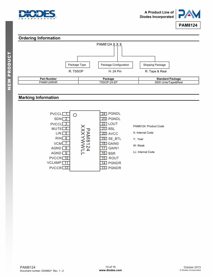
Pin Assignments TSSOP-24-EP
PVCCLSDN
PVCCLMUTE
LIN
VCMAGNDAGND
PVCCRVCLAMP
PVCCR PGNDRPGNDRROUTBSRGAIN1GAIN0
AVCCBSLLOUTPGNDLPGNDL
PA
M8124
XX
XY
WW
LL 17
123456789101112 13
141516
18192021222324
RIN SE_BTL
Applications • Televisions • Home Sound Systems • Active Speakers
Typical Applications Circuit
PVCCL1
SDN2
PVCCL3
MUTE4
LIN5
RIN6
VCM7
AGND8
AGND9
PVCCR10
VCLAMP11
PVCCR12 PGNDR 13
PGNDR 14
ROUT 15
BSR 16
GAIN1 17
GAIN0 18
SE_BTL 19
AVCC 20
BSL 21
LOUT 22
PGNDL 23
PGNDL 24
U1
SD
Mute
C11uF
C31uF
C5220nF
L1
33uH
G0
C2 1uF
G1
R14.7K C7
470uF
L_out1
8ohm
C6220nF
L2
33uH
C4 1uF
R24.7K
C8470uF R_out1
8ohm
L_in
R_in
PAM
8124
10V_to_26V
10V_to_26V
SE_BTL
10V_to_26V

PAM8124 Document number: DS36627 Rev. 1 - 2
2 of 15 www.diodes.com
October 2013© Diodes Incorporated
PAM8124
NE
W P
RO
DU
CT
A Product Line of
Diodes Incorporated
Pin Descriptions
Pin Name I/O/P Function 1, 3 PVCCL P Power supply for left channel H-bridge, not connected to PVCCR or AVCC
2 SDN I Shutdown signal for IC (low = shutdown, high = operational). TTL logic levels with compliance to AVCC
4 MUTE I A logic high on this pin disables the outputs. A low on this pin enables the outputs. TTL logic levels with compliance to AVCC
5 LIN I Audio input for left channel 6 RIN I Audio input for right channel 7 VCM O Reference for analog cells
8, 9 AGND P Analog ground for digital/analog cells in core 10, 12 PVCCR P Power supply for right channel H-bridge, not connected to PVCCL or AVCC
11 VCLAMP P Internally generated voltage supply for bootstrap. Not to be used as a supply or connected to any component other than the decoupling capacitor.
13, 14 PGNDR P Power ground for right channel H-bridge 15 ROUT O Class-D H-bridge output for right channel 16 BSR I/O Bootstrap I /O for right channel H-bridge 17 GAIN1 I Gain select most-significant bit. TTL logic levels with compliance to AVCC 18 GAIN0 I Gain select least-significant bit. TTL logic levels with compliance to AVCC
19 SE_BTL I A logic low on this pin enables one single-ended input in BTL configuration. A logic high on this pin enables two inputs in SE/BTL configuration. TTL logic levels with compliance to AVCC
20 AVCC P High-voltage analog power supply 21 BSL I/O Bootstrap I /O for left channel H-bridge 22 LOUT O Class-D H-bridge output for left channel
23, 24 PGNDL P Power ground for left channel H-bridge
Functional Block Diagram

PAM8124 Document number: DS36627 Rev. 1 - 2
3 of 15 www.diodes.com
October 2013© Diodes Incorporated
PAM8124
NE
W P
RO
DU
CT
A Product Line of
Diodes Incorporated
Absolute Maximum Ratings (@TA = +25°C, unless otherwise specified.)
Parameter Rating Unit Supply Voltage (VCC) 28 V Logic Input Voltage (SDN, MUTE, GAIN0, GAIN1, SE_BTL) -0.3 to VCC +0.3 V Analog Input Voltage (LIN, RIN) -0.3 to +5.5 V Storage Temperature -65 to +150 °C Maximum Junction Temperature 150 °C Junction to ambient thermal resistance 40 °C/W
Recommended Operating Conditions (@TA = +25°C, unless otherwise specified.)
Symbol Parameter Min Max Unit VCC Supply Voltage 10 26 V
TA Operating Ambient Temperature Range -40 +85 °C
TJ Junction Temperature Range -40 +125 °C
Electrical Characteristics (@TA = +25°C, VCC = 24V, Gain = 20dB, RL = 8Ω unless otherwise specified.)
Symbol Parameter Test Conditions Min Typ Max Units
|VOS| Class-D output offset voltage(measured differently) Vi = 0V, AV = 36dB 20 100 mV
ICC(q) Quiescent supply current SDN = 2.5V, MUTE = 0V, No Load 25 40 mA
ICC(MUTE) Quiescent supply current in mute mode MUTE = 2.5V, No load 25 40 mA
ICC(SDN) Quiescent current in shutdown mode SDN = 0.8V, No load 30 60 µA
RDS(ON) Drain-source on-state resistance IO = 0.5A 150 mΩ
G Gain
GAIN1 = 0.8V, GAIN0 = 0.8V 18 20 22
dB GAIN1 = 0.8V, GAIN0 = 2.5V 24 26 28 GAIN1 = 2.5V, GAIN0 = 0.8V 30 32 34 GAIN1 = 2.5V, GAIN0 = 2.5V 34 36 38
Mute Attenuation Vi = 1Vrms -60 dB
PSRR Power Supply Rejection Ratio VRIPPLE = 200mVpp, f = 1kHz,gain = 20dB
-52 dB
PO
Output Power at 1% THD+N RL = 4Ω, f = 1kHz 14
W RL = 8Ω, f = 1kHz 8
Output Power at 10% THD+N RL = 4Ω, f = 1kHz 18
RL = 8Ω, f = 1kHz 10
THD+N Total harmonic distortion + noise RL =4Ω, f = 1kHz, Po = 10W 0.15
% RL = 8Ω, f = 1kHz, Po = 5W 0.08
Vn Output integrated noise floor 20Hz to 22kHz, A-weighted, Gain = 20dB 200 µV
Cs Crosstalk PO = 1W, f = 1kHz, Gain = 20dB -70 dB SNR Signal-to-noise ratio THD+N<1%, f = 1kHz, Gain = 20dB 92 dB OTP Thermal trip point 160 °C OTH Thermal hysteresis 60 °C
fosc Oscillator frequency SE_BTL = 2.5V 250 300 350
kHz SE_BTL = 0.8V 360

PAM8124 Document number: DS36627 Rev. 1 - 2
4 of 15 www.diodes.com
October 2013© Diodes Incorporated
PAM8124
NE
W P
RO
DU
CT
A Product Line of
Diodes Incorporated
0.02
20
0.05
0.1
0.2
0.5
1
2
5
10
%
20 20k50 100 200 500 1k 2k 5k 10kHz
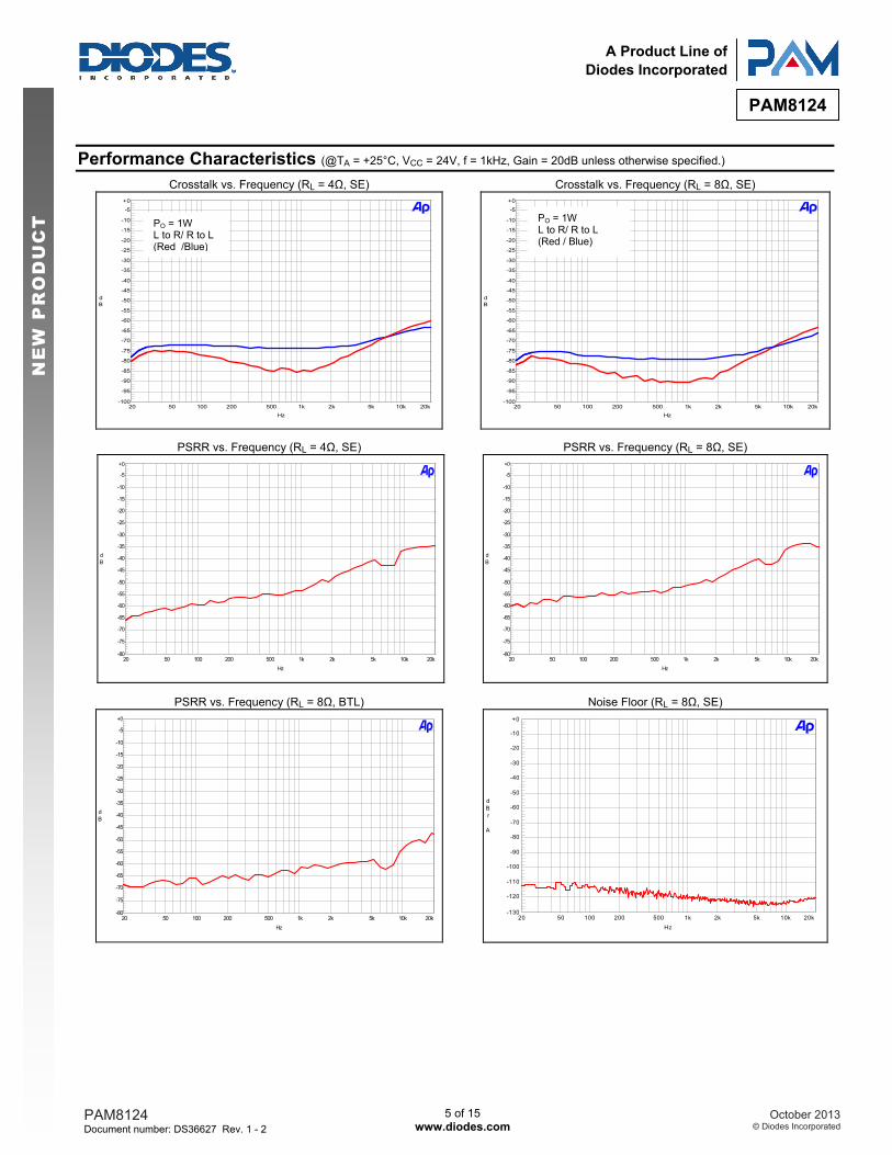
Performance Characteristics (@TA = +25°C, VCC = 24V, f = 1kHz, Gain = 20dB unless otherwise specified.) THD+N vs. Output Power (RL = 4Ω, SE)
0.06
20
0.1
0.2
0.5
1
2
5
10
%
1m 302m 5m 10m 20m 50m 100m 200m 500m 1 2 5 10 20W
THD+N vs. Output Power (RL = 8Ω, SE)
0.03
20
0.05
0.1
0.2
0.5
1
2
5
10
%
1m 202m 5m 10m 20m 50m 100m 200m 500m 1 2 5 10W
THD+N vs. Frequency (RL = 4Ω, SE)
0.03
20
0.05
0.1
0.2
0.5
1
2
5
10
%
20 20k50 100 200 500 1k 2k 5k 10kHz
THD+N vs. Frequency (RL = 8Ω, SE)
THD+N vs. Output Power (RL = 8Ω, BTL)
0.03
20
0.05
0.1
0.2
0.5
1
2
5
10
%
1m 502m 5m 10m 20m 50m 100m 200m 500m 1 2 5 10 20W
THD+N vs. Frequency (RL = 8Ω, BTL)
0.01
20
0.02
0.05
0.1
0.2
0.5
1
2
5
10
%
20 20k50 100 200 500 1k 2k 5k 10kHz
PO = 1W/ 2W/ 6W (Red / Blue/ Pink)
PO = 5W/ 10W/ 15W (Red / Blue/ Pink)
PO = 2W/ 5W/ 8W (Red / Blue/ Pink)
PAM8124 Document number: DS36627 Rev. 1 - 2
5 of 15 www.diodes.com
October 2013© Diodes Incorporated
PAM8124
NE
W P
RO
DU
CT
A Product Line of
Diodes Incorporated
Performance Characteristics (@TA = +25°C, VCC = 24V, f = 1kHz, Gain = 20dB unless otherwise specified.) Crosstalk vs. Frequency (RL = 4Ω, SE)
-100
+0
-95
-90
-85
-80
-75
-70
-65
-60
-55
-50
-45
-40
-35
-30
-25
-20
-15
-10
-5
dB
20 20k50 100 200 500 1k 2k 5k 10kHz
Crosstalk vs. Frequency (RL = 8Ω, SE)
-100
+0
-95
-90
-85
-80
-75
-70
-65
-60
-55
-50
-45
-40
-35
-30
-25
-20
-15
-10
-5
dB
20 20k50 100 200 500 1k 2k 5k 10kHz
T T
PSRR vs. Frequency (RL = 4Ω, SE)
-80
+0
-75
-70
-65
-60
-55
-50
-45
-40
-35
-30
-25
-20
-15
-10
-5
dB
20 20k50 100 200 500 1k 2k 5k 10kHz
T T
PSRR vs. Frequency (RL = 8Ω, SE)
-80
+0
-75
-70
-65
-60
-55
-50
-45
-40
-35
-30
-25
-20
-15
-10
-5
dB
20 20k50 100 200 500 1k 2k 5k 10kHz
T T T
PSRR vs. Frequency (RL = 8Ω, BTL)
-80
+0
-75
-70
-65
-60
-55
-50
-45
-40
-35
-30
-25
-20
-15
-10
-5
dB
20 20k50 100 200 500 1k 2k 5k 10kHz
T T T T T T
Noise Floor (RL = 8Ω, SE)
-130
+0
-120
-110
-100
-90
-80
-70
-60
-50
-40
-30
-20
-10
dBr A
20 20k50 100 200 500 1k 2k 5k 10kHz
PO = 1W L to R/ R to L (Red /Blue)
PO = 1W L to R/ R to L (Red / Blue)
PAM8124 Document number: DS36627 Rev. 1 - 2
6 of 15 www.diodes.com
October 2013© Diodes Incorporated
PAM8124
NE
W P
RO
DU
CT
A Product Line of
Diodes Incorporated
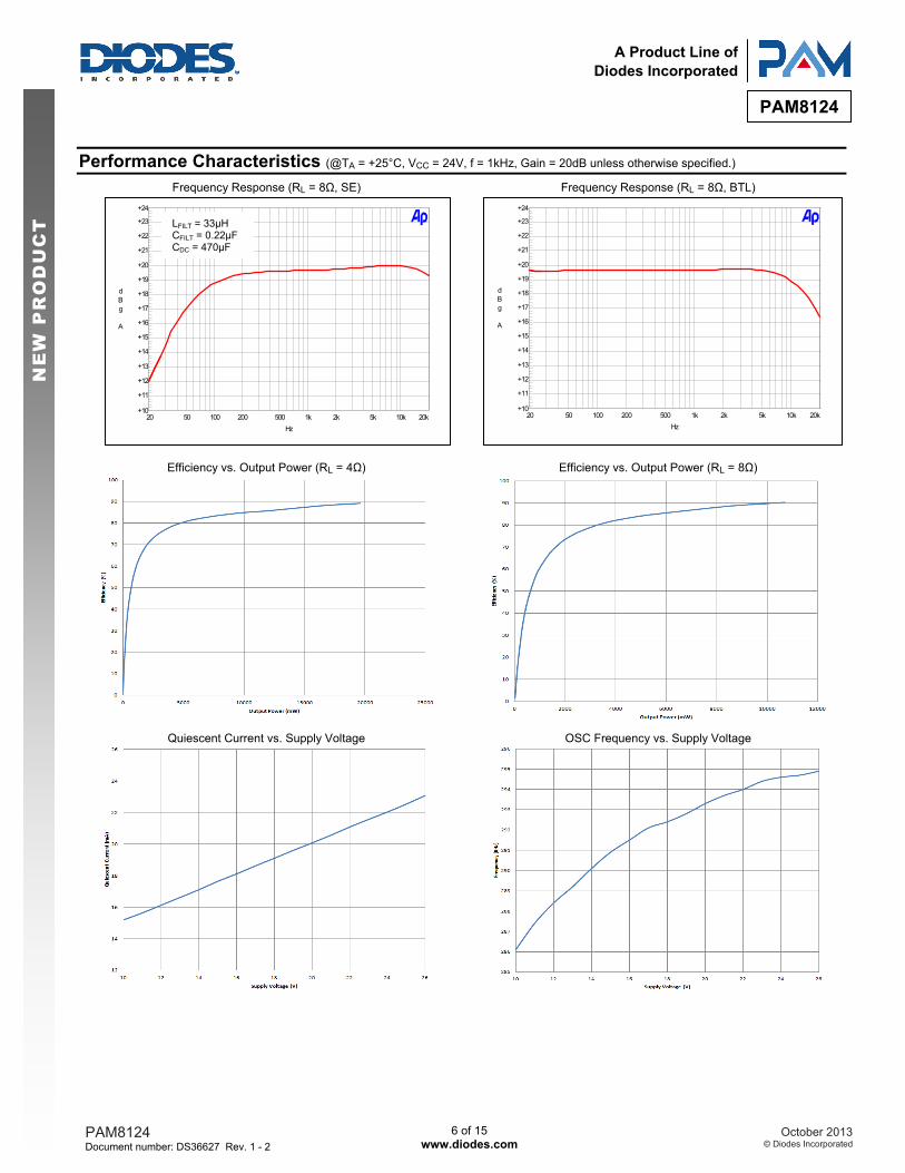
Performance Characteristics (@TA = +25°C, VCC = 24V, f = 1kHz, Gain = 20dB unless otherwise specified.) Frequency Response (RL = 8Ω, SE)
Frequency Response (RL = 8Ω, BTL)
Efficiency vs. Output Power (RL = 4Ω)
Efficiency vs. Output Power (RL = 8Ω)
Quiescent Current vs. Supply Voltage OSC Frequency vs. Supply Voltage
+10
+24
+11
+12
+13
+14
+15
+16
+17
+18
+19
+20
+21
+22
+23
dBg A
20 20k50 100 200 500 1k 2k 5k 10kHz
LFILT = 33µH CFILT = 0.22µF CDC = 470µF
+10
+24
+11
+12
+13
+14
+15
+16
+17
+18
+19
+20
+21
+22
+23
dBg A
20 20k50 100 200 500 1k 2k 5k 10kHz

PAM8124 Document number: DS36627 Rev. 1 - 2
7 of 15 www.diodes.com
October 2013© Diodes Incorporated
PAM8124
NE
W P
RO
DU
CT
A Product Line of
Diodes Incorporated
Performance Characteristics (@TA = +25°C, VCC = 24V, f = 1kHz, Gain = 20dB unless otherwise specified.) Case Temperature vs. Output Power (RL = 4Ω) Case Temperature vs. Output Power (RL = 8Ω)
Application Information Input Capacitors (Ci) In the typical application, an input capacitor Ci, is required to allow the amplifier to bias the input signal to the proper DC level for optimum operation. In this case, Ci and the minimum input impedance Ri form is a high-pass filter with the corner frequency determined in the follow equation:
( )C
1f2 RiCiπ
=
It is important to consider the value of Ci as it directly affects the low frequency performance of the circuit. For example, when Ri is 40kΩ and the specification calls for a flat bass response are down to 20Hz. Equation is reconfigured as followed:
( )i c
1Ci2 Rfπ
=
When input resistance variation is considered Ci is 200nF, so one would likely choose a value of 220nF. A further consideration for this capacitor is the leakage path from the input source through the input network (Ci, Ri + Rf) to the load. This leakage current creates a DC offset voltage at the input to the amplifier that reduces useful headroom, especially in high gain applications. For this reason, a low-leakage tantalum or ceramic capacitor is the best choice. Gain Setting Control The gain of the PAM8124 is set by two input terminals, GAIN0 and GAIN1. The gains listed in following table are realized by changing the taps on the input resistors inside the amplifier. This causes the input impedance to be dependent on the gain setting. The actual gain settings are controlled by ratios of resistors, so the gain variation from part-to-part is small. However, the input impedance from part-to-part at the same gain may shift by ±20% due to shifts in the actual resistance of the input resistors. Table 1: Gain Setting
Gain1 Gain0 Amplifier Gain (dB), Typical
Input Impedance (kΩ),Typical (Ri)
0 0 20 40 0 1 26 20 1 0 30 10 1 1 36 6.67
Two Channels Driving Two Channels Driving

PAM8124 Document number: DS36627 Rev. 1 - 2
8 of 15 www.diodes.com
October 2013© Diodes Incorporated
PAM8124
NE
W P
RO
DU
CT
A Product Line of
Diodes Incorporated
Application Information (cont.) Input Resistance Changing the gain setting can vary the input resistance of the amplifier from its smallest value (6.67kΩ ±20%) to the largest value (40kΩ ±20%). As a result, if a single capacitor is used in the input high-pass filter, the –3dB cutoff frequency may change when changing gain steps. The –3dB frequency can be calculated using the following Equation. Use the Ri values given in Table 1.
( )C
1f2 RiCiπ
=
Single-Ended Output Capacitor In single-ended (SE) applications, the dc blocking capacitor forms a high-pass filter with the speaker impedance. The frequency response rolls off with decreasing frequency at a rate of 20dB/decade. The cutoff frequency is determined by:
SELcoh CRf
π21
=
Table 2 shows some common component values and the associated cutoff frequencies: Table 2: Common Filter Responses
RL-Speaker Impedance (Ω) CSE-DC Blocking Capacitor (µF)
fc = 60Hz (-3dB) fc = 40Hz (-3dB) fc = 20Hz (-3dB) 4 680 1000 2200 6 470 680 1500 8 330 470 1000
Output Filter and Frequency Response For the best frequency response, a flat pass band output filter (second-order Butterworth) may be used. The output filter components consist of the series inductor and capacitor to ground at the LOUT and ROUT pins. There are several possible configurations, depending on the speaker impedance and whether the output configuration is single-ended (SE) or bridge-tied load (BTL). Table 3 lists the recommended values for the filter components. It is important to use a high-quality capacitor in this application. A rating of at least X7R is required. Table 3: Recommended Filter Output Components
Output Configuration Speaker Impedance(Ω) Filter Inductor(µH) Filter Capacitor(nF)
Single Ended (SE) 4 22 680 8 33 220
Bridge Tied Load (BTL) 8 22 680

PAM8124 Document number: DS36627 Rev. 1 - 2
9 of 15 www.diodes.com
October 2013© Diodes Incorporated
PAM8124
NE
W P
RO
DU
CT
A Product Line of
Diodes Incorporated
Application Information (cont.)
BTL Filter Configuration SE Filter Configuration
Power and Heat Dissipation Choose speakers that are able to stand large output power from the PAM8124. Otherwise, speaker may suffer damage. Heat dissipation is very important when the device works in full power operation. Two factors affect the heat dissipation, the efficiency of the device that determines the dissipation power, and the thermal resistance of the package that determines the heat dissipation capability. Generally, class-D amplifiers are high efficiency and need no heat sink. Operating at higher powers a heat sink still may not be necessary if the PCB is carefully designed to achieve good thermal dissipation. How to Reduce EMI Most applications require a ferrite bead filter for EMI elimination shown at Figure 1. The ferrite filter reduces EMI around 1MHz and higher. When selecting a ferrite bead, choose one with high impedance at high frequencies, but low impedance at low frequencies.
200pF
200pF
OUT+
OUT-
Ferrite Bead
Ferrite Bead
Figure 1. Ferrite Bead Filter to Reduce EMI
Dual-Side PCB To achieve good heat dissipation, the PCB's copper plate should be thicker than 35um and the copper plate on both sides of the PCB should be utilized for heat sink. The thermal pad on the bottom of the device should be soldered to the plate of the PCB, and via holes, usually 9 to 16, should be drilled in the PCB area under the device and deposited copper on the vias should be thick enough so that the heat can be dissipated to the other side of the plate. There should be no insulation mask on the other side of the copper plate. It is better to drill more vias on the PCB around the device if possible.

PAM8124 Document number: DS36627 Rev. 1 - 2
10 of 15 www.diodes.com
October 2013© Diodes Incorporated
PAM8124
NE
W P
RO
DU
CT
A Product Line of
Diodes Incorporated
Application Information (cont.) MUTE Operation The MUTE pin is an input for controlling the output state of the PAM8124. A logic high on this pin causes the outputs to run at a constant 50% duty cycle. A logic low on this pin enables the outputs. This pin may be used as a quick disable or enable of the outputs. Shutdown Operation The PAM8124 employs a shutdown operation mode to reduce supply current to the absolute minimum level during periods of non-use to save power. The SDN input terminal should be pulling high during normal operation when the amplifier is in use. Pulling SDN low causes the outputs to mute and the amplifier to enter a low-current state. SDN should never be left unconnected to prevent the amplifier from unpredictable operation. For the best power-off pop performance, the amplifier should be set in shutdown mode prior to removing the power supply voltage. For the best start-up pop performance, the amplifier should be set in mute mode prior to restarting the amplifier. Internal Bias Generator Capacitor Selection The internal bias generator (VCM) provides the internal bias for the preamplifier stage. The external input capacitors and this internal reference allow the inputs to be biased within the optimal common-mode range of the input preamplifiers. The selection of the capacitor value on the VCM terminal is critical for achieving the best device performance. During startup or recovery from shutdown state the VCM capacitor determines the rate at which the amplifier starts up. The startup time is not critical for the best de-pop performance since any heard pop sound is the result of the class-D output switching-on other than that of the startup time. However, at least a 0.47µF capacitor is recommended for the VCM capacitor. Another function of the VCM capacitor is to bypass high frequency noise on the internal bias generator. Power Supply Decoupling, CS The PAM8124 is a high-performance CMOS audio amplifier that requires adequate power supply decoupling to ensure the output total harmonic distortion (THD) as low as possible. Power supply decoupling also prevents oscillations caused by long lead between the amplifier and the speaker. The optimum decoupling is achieved by using two capacitors of different types that target different types of noise on the power supply leads. For higher frequency transients, spikes, or digital hash on the line, a good low equivalent-series-resistance (ESR) ceramic capacitor of 0.1µF is typically recommended, placed as close as possible to the device's PVCC lead. To filter lower-frequency noises a large aluminium electrolytic capacitor of 470µF or greater is recommended, placed near the audio power amplifier. The 10µF capacitor also serves as a local storage capacitor for supplying current during large signal transients on the amplifier outputs. BSL and BSR Capacitors The half H-bridge output stages use NMOS transistors therefore requiring bootstrap capacitors for the high side of each output to turn on correctly. A ceramic capacitor 220nF or more rated for over 25V must be connected from each output to its corresponding bootstrap input. Specifically, one 220nF capacitor must be connected from LOUT to BSL and another 220nF capacitor from ROUT to BSR. It is recommended to use 1μF BST capacitor to replace 220nF for lower than 100Hz applications. VCLAMP Capacitors To ensure that the maximum gate-to-source voltage for the NMOS output transistors is not exceeded, an internal regulator is used to clamp the gate voltage. A 1µF capacitor must be connected from VCLAMP to ground and must be rated for at least 25V. The voltages at the VCLAMP terminals vary with VCC and may not be used to power any other circuitry. Using Low-ESR Capacitors Low-ESR capacitors are recommended throughout this application section. A real (with respect to ideal) capacitor can be modeled simply as a resistor in series with an ideal capacitor. The voltage drop across this resistor minimizes the beneficial effects of the capacitor in the circuit. The lower the equivalent value of this resistance the more the real capacitor behaves as an ideal capacitor. Short-Circuit Protection The PAM8124 has short circuit protection circuitry on the outputs to prevent damage to the device when output-to-output shorts (BTL mode), output-to-GND shorts, or output-to-VCC shorts occur. Once a short-circuit is detected on the outputs, the output drive is immediately disabled. This is not a latched fault. If the short was removed, the normal operation is restored.

PAM8124 Document number: DS36627 Rev. 1 - 2
11 of 15 www.diodes.com
October 2013© Diodes Incorporated
PAM8124
NE
W P
RO
DU
CT
A Product Line of
Diodes Incorporated
Application Information (cont.) Thermal Protection Thermal protection on the PAM8124 prevents damage to the device when the internal die temperature exceeds 160°C. There is a ±15 degree tolerance on this trip point from device to device. Once the die temperature exceeds the set thermal point, the device enters into the shutdown state and the outputs are disabled. This is not a latched fault, the thermal fault is cleared once the temperature of the die is reduced by 60°C. The device begins normal operation at this point without external system intervention. Over Voltage Protection and Under Voltage Lock-out (OVP and UVLO) An over voltage protection (OVP) circuit is integrated in PAM8124, when the supply voltage is over 28V the OVP is active and then the output stage is disabled. The PAM8124 will auto recovery when the supply voltage is lower than the OVP threshold. The PAM8124 incorporates circuitry designed to detect low supply voltage. When the supply voltage drops to 9V or below, the PAM8124 goes into a state of shutdown. When the supply voltage is higher than UVLO threshold normal operation is resumed.
Typical Applications Circuits
PVCCL1
SDN2
PVCCL3
MUTE4
LIN5
RIN6
VCM7
AGND8
AGND9
PVCCR10
VCLAMP11
PVCCR12 PGNDR 13
PGNDR 14
ROUT 15
BSR 16
GAIN1 17
GAIN0 18
SE_BTL 19
AVCC 20
BSL 21
LOUT 22
PGNDL 23
PGNDL 24
U1
C1010uF
C70.1uF
C1210uF
C90.1uF
C14470uF
C13470uF
SD
R1Mute
R2C1 1uF
C2 1uF
C41uF
C31uF
C15220nF
L1
33uH
G0
C5 1uF
C80.1uF
G1
C1110uF
VCC
VCC
VCC
R34.7K C17
470uF
L_out
8ohm
C16220nF
L2
33uH
C6 1uF
R44.7K
C18470uF R_out
8ohm
L_in
R_in
PAM
8124
Schematic for Single-Ended (SE) Configuration (8Ω Speaker)

PAM8124 Document number: DS36627 Rev. 1 - 2
12 of 15 www.diodes.com
October 2013© Diodes Incorporated
PAM8124
NE
W P
RO
DU
CT
A Product Line of
Diodes Incorporated
Application Information (cont.) Typical Applications Circuits (cont.)
PVCCL1
SDN2
PVCCL3
MUTE4
LIN5
RIN6
VCM7
AGND8
AGND9
PVCCR10
VCLAMP11
PVCCR12 PGNDR 13
PGNDR 14
ROUT 15
BSR 16
GAIN1 17
GAIN0 18
SE_BTL 19
AVCC 20
BSL 21
LOUT 22
PGNDL 23
PGNDL 24
U1
C1010uF
C70.1uF
C1210uF
C90.1uF
C14470uF
C13470uF
SD
R1Mute
R2C1 1uF
C2 1uF
C41uF
C31uF
C15680nF
L1
22uH
G0
C5 1uF
C80.1uF
G1
C1110uF
VCC
VCC
VCC
R34.7K
8ohm
C16680nF
L2
22uH
C6 1uF
R44.7K
IN+
IN-
PAM
8124
Schematic for Bridge-Tied-Load (BTL) Configuration with Differential Input (8Ω Speaker)
PVCCL1
SDN2
PVCCL3
MUTE4
LIN5
RIN6
VCM7
AGND8
AGND9
PVCCR10
VCLAMP11
PVCCR12 PGNDR 13
PGNDR 14
ROUT 15
BSR 16
GAIN1 17
GAIN0 18
SE_BTL 19
AVCC 20
BSL 21
LOUT 22
PGNDL 23
PGNDL 24
U1
C1010uF
C70.1uF
C1210uF
C90.1uF
C14470uF
C13470uF
SD
R1Mute
C1 1uF
C41uF
C31uF
C15680nF
L1
22uH
G0
C5 1uF
C80.1uF
G1
C1110uF
VCC
VCC
VCC
R34.7K
8ohm
C16680nF
L2
22uH
C6 1uF
R44.7K
IN
PAM
8124
Schematic for Bridge-Tied-Load (BTL) Configuration with Single-Ended Input (8Ω Speaker)
PAM8124 Document number: DS36627 Rev. 1 - 2
13 of 15 www.diodes.com
October 2013© Diodes Incorporated
PAM8124
NE
W P
RO
DU
CT
A Product Line of
Diodes Incorporated
Ordering Information PAM8124 X X X
R: TSSOP H: 24 Pin R: Tape & Real
Part Number Package Standard Package PAM8124RHR TSSOP-24-EP 3000 Units/Tape&Reel
Marking Information
PVCCLSDN
PVCCLMUTE
LIN
VCMAGNDAGND
PVCCRVCLAMP
PVCCR PGNDRPGNDRROUTBSRGAIN1GAIN0
AVCCBSLLOUTPGNDLPGNDL
PA
M8124
XX
XY
WW
LL 17
123456789101112 13
141516
18192021222324
RIN SE_BTL
PAM8124: Product Code X: Internal Code
Y: Year
W: Week
LL: Internal Code
Package Configuration Shipping Package Package Type

PAM8124 Document number: DS36627 Rev. 1 - 2
14 of 15 www.diodes.com
October 2013© Diodes Incorporated
PAM8124
NE
W P
RO
DU
CT
A Product Line of
Diodes Incorporated
Package Outline Dimensions (All dimensions in mm.) Package: TSSOP-24-EP
PAM8124 Document number: DS36627 Rev. 1 - 2
15 of 15 www.diodes.com
October 2013© Diodes Incorporated
PAM8124
NE
W P
RO
DU
CT
A Product Line of
Diodes Incorporated
IMPORTANT NOTICE DIODES INCORPORATED MAKES NO WARRANTY OF ANY KIND, EXPRESS OR IMPLIED, WITH REGARDS TO THIS DOCUMENT, INCLUDING, BUT NOT LIMITED TO, THE IMPLIED WARRANTIES OF MERCHANTABILITY AND FITNESS FOR A PARTICULAR PURPOSE (AND THEIR EQUIVALENTS UNDER THE LAWS OF ANY JURISDICTION). Diodes Incorporated and its subsidiaries reserve the right to make modifications, enhancements, improvements, corrections or other changes without further notice to this document and any product described herein. Diodes Incorporated does not assume any liability arising out of the application or use of this document or any product described herein; neither does Diodes Incorporated convey any license under its patent or trademark rights, nor the rights of others. Any Customer or user of this document or products described herein in such applications shall assume all risks of such use and will agree to hold Diodes Incorporated and all the companies whose products are represented on Diodes Incorporated website, harmless against all damages. Diodes Incorporated does not warrant or accept any liability whatsoever in respect of any products purchased through unauthorized sales channel. Should Customers purchase or use Diodes Incorporated products for any unintended or unauthorized application, Customers shall indemnify and hold Diodes Incorporated and its representatives harmless against all claims, damages, expenses, and attorney fees arising out of, directly or indirectly, any claim of personal injury or death associated with such unintended or unauthorized application. Products described herein may be covered by one or more United States, international or foreign patents pending. Product names and markings noted herein may also be covered by one or more United States, international or foreign trademarks. This document is written in English but may be translated into multiple languages for reference. Only the English version of this document is the final and determinative format released by Diodes Incorporated.
LIFE SUPPORT Diodes Incorporated products are specifically not authorized for use as critical components in life support devices or systems without the express written approval of the Chief Executive Officer of Diodes Incorporated. As used herein: A. Life support devices or systems are devices or systems which: 1. are intended to implant into the body, or
2. support or sustain life and whose failure to perform when properly used in accordance with instructions for use provided in the labeling can be reasonably expected to result in significant injury to the user.
B. A critical component is any component in a life support device or system whose failure to perform can be reasonably expected to cause the failure of the life support device or to affect its safety or effectiveness. Customers represent that they have all necessary expertise in the safety and regulatory ramifications of their life support devices or systems, and acknowledge and agree that they are solely responsible for all legal, regulatory and safety-related requirements concerning their products and any use of Diodes Incorporated products in such safety-critical, life support devices or systems, notwithstanding any devices- or systems-related information or support that may be provided by Diodes Incorporated. Further, Customers must fully indemnify Diodes Incorporated and its representatives against any damages arising out of the use of Diodes Incorporated products in such safety-critical, life support devices or systems. Copyright © 2013, Diodes Incorporated www.diodes.com