Embed Size (px)
DESCRIPTION
PADS Layout Tutorial
Citation preview
PADS Layout Tutorial
Note: This tutorial is modified from the original tutorial to bring it up to date for version 9.1 and to expand on some additional features that may be useful for ECE477 senior design students. The original tutorials are located at: http://www.people.vcu.edu/~rhklenke/tutorials/PADS/PADS_Tutorial_3.3V_Reg/SimpleReg.html http://www.people.vcu.edu/~rhklenke/tutorials/PADS/PADS_Tutorial_New_Part/NewPartType.html What you will learn:
• Creating a Circuit Schematic with PADS Logic • Creating a PCB Design with PADS Layout • Routing a PCB Design with PADS Router • Linking PADS Logic to PADS Layout & PADS Router • Generating Gerber Files with PADS Layout
Note: This tutorial assumes that you've completed the PADS User Interface tutorial and the New Part Type tutorial.
Example: Creating a simple 5V Regulator Circuit using PADS 1. Creating a Circuit Schematic using PADS Logic
1.1 Begin by opening PADS Logic. Select Start > Programs > ECN Software > Mentor Graphics SDD > PADS 9.1 > Design Entry > PADS Logic.

1.2 Ensure that your user library is available by using the library manager. Click File > Library and select the Manage Lib List… button and verify that your library is accessible. 1.3 Start a new design by selecting File > New. Your PADS Logic window should look something like this.
1.4 Use the Add Part window to add an LM2675 voltage regulator to your design. To add
a part to your design, click on the button on the design toolbar. This will open the Add Part from Library window as shown below. If a Question window pops up requesting a Component Alpha-Prefix for the part type here, type U .

To locate the LM2675 part, you will need to select your custom library from the Library dropdown list in the filter box. Select N:\(Pads Library) Ensure that the Items field contains a single asterisk * and then press Apply. This will filter the results, displaying only the parts in your user library. The window should look similar to the one above. Press the Add button. An outline of the LM2675 part will appear below the mouse pointer while it is within the design window. Close the Add Part window and click somewhere near the center of the sheet to add an instance of the LM2675 part. Press ESC to exit add part mode. You schematic window should look similar to the one below.
1.5 Add capacitors to your design.
Tool Note: You may wish to zoom in and out on the decal while making changes to the pins. Several methods may be used to zoom: 1. To enter zoom mode, press Ctrl + W. Use the left mouse button to zoom in and the right mouse button to zoom out. Press Esc to exit zoom mode. 2. On a roller-button mouse you can also hold the roller button down and drag to zoom in and out: drag up to zoom in and down to zoom out. 3. CTRL + scroll wheel will zoom in
and out.
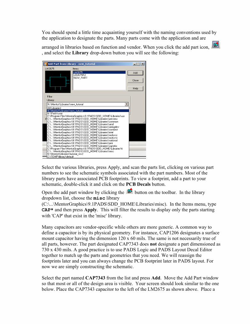
You should spend a little time acquainting yourself with the naming conventions used by the application to designate the parts. Many parts come with the application and are
arranged in libraries based on function and vendor. When you click the add part icon, , and select the Library drop-down button you will see the following:
Select the various libraries, press Apply, and scan the parts list, clicking on various part numbers to see the schematic symbols associated with the part numbers. Most of the library parts have associated PCB footprints. To view a footprint, add a part to your schematic, double-click it and click on the PCB Decals button.
Open the add part window by clicking the button on the toolbar. In the library dropdown list, choose the misc library (C:\...\MentorGraphics\9.1PADS\SDD_HOME\Libraries\misc). In the Items menu, type CAP* and then press Apply. This will filter the results to display only the parts starting with 'CAP' that exist in the 'misc' library. Many capacitors are vendor-specific while others are more generic. A common way to define a capacitor is by its physical geometry. For instance, CAP1206 designates a surface mount capacitor having the dimension 120 x 60 mils. The same is not necessarily true of all parts, however. The part designated CAP7343 does not designate a part dimensioned as 730 x 430 mils. A good practice is to use PADS Logic and PADS Layout Decal Editor together to match up the parts and geometries that you need. We will reassign the footprints later and you can always change the PCB footprint later in PADS layout. For now we are simply constructing the schematic. Select the part named CAP7343 from the list and press Add. Move the Add Part window so that most or all of the design area is visible. Your screen should look similar to the one below. Place the CAP7343 capacitor to the left of the LM2675 as shown above. Place a

second CAP7343 to the far right as shown in the schematic below. Press ESC to leave the insert mode.
Now select CAP1206 from the Add Part window, press Add and close the window. Before adding the capacitor to your design, right-click the mouse and select Rotate 90 to turn the symbol. Place the capacitor to the right of the LM2675 as shown below.
1.6 Add additional circuit components to your design. Add an inductor and diode to your design as shown in the image below. Use the IND-MOLDED part for the inductor and the DIODE part for the diode. Both of these parts are found in the misc library. Use IND* and DIODE* to search the library

1.7 Assign values to your components. Ensure that part selection is enabled by right clicking in an empty area and selecting the
Select Gates option. This can also be achieved by pressing the button on the filter toolbar. Double-click on the left-most capacitor. This will open the Part Properties window as shown below.
Click on the Attributes button to open the Part Attributes window. Notice that when you move the cursor over the Description that the full Value is displayed.

Scroll down to the Value field, click the Edit button and enter 15uF in the text box.
Press OK to close the Part Attributes window and return to the Part Properties window. By default, the CAP7343 part will not display its value in the schematic. To change this, click the Visibility button to open the Part Text Visibility window.
Check the Value checkbox on the right side to enable display of the capacitor's value. Press OK to close the Part Text Visibility window and then press Close to close the Part Properties window. Repeat this process for the other components, assigning the values listed below:
• Right Capacitor - 33uF • Middle Capacitor - 0.01uF • Inductor - 33uH
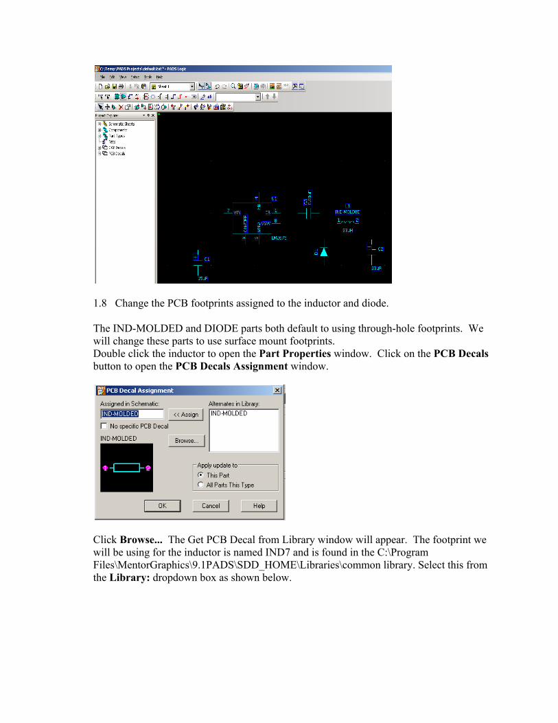
1.8 Change the PCB footprints assigned to the inductor and diode. The IND-MOLDED and DIODE parts both default to using through-hole footprints. We will change these parts to use surface mount footprints. Double click the inductor to open the Part Properties window. Click on the PCB Decals button to open the PCB Decals Assignment window.
Click Browse... The Get PCB Decal from Library window will appear. The footprint we will be using for the inductor is named IND7 and is found in the C:\Program Files\MentorGraphics\9.1PADS\SDD_HOME\Libraries\common library. Select this from the Library: dropdown box as shown below.

Select this decal and press OK. Then press OK in the PCB Decal Assignment window and Close the Part Properties window. Repeat this process for the diode, selecting the DIODE2 footprint from the 'common' library. 1.9 Adding Header Pins to your design. We will now add a pair of 2-pin headers to the schematic. One 2-pin header will be used for the input voltage source (12V), and the other will be used for the 5V output.
Open the Add Part window by clicking . Select the 'connect' library from the dropdown list and enter HEADER* in the Items filter. Press Apply and select HEADER02 .
PADS implements connectors as if they were multi-gate IC's. In this case, each pin is treated as a separate gate and must be added individually. Add two header pins to the left of the schematic, and two to the right (Use Ctrl+F to mirror a part horizontally). Your schematic should look similar to the one below. Notice the pin designations; the two-pin header on the left is designated J1 with pins 1 and 2, the right connector designated J2 with pins 1 and 2.

1.10 Connecting your parts.
Press the Add Connection, , button on the design toolbar. This will activate the connection mode. Place the cursor on pin 7 of the LM2675 and click once to begin adding a connection. Move the cursor to the left until it is vertically aligned with the left capacitor. Click once. This will add a vertex / pivot point to your connection. Move the cursor down and click on the top terminal of the left capacitor to complete the connection. Your schematic should look like the image below.
Continue adding connections until your schematic is fully connected as shown below.

To delete a connection, activate Delete by pressing the button on the design toolbar. This will allow you to remove objects with a single click.
To move a part click Move, , and re-place the device. If it has connections they will remain attached to the component during transition.
Not the connection between D1 and C3, shown belowon the left. This type of connection is discouraged since it may be confused with two connections which cross but do not connect. The connections shown below on the right are the preferred way to illustrate connections of this type.
1.11 Adding Power and Ground Connections To add a ground connection to your design, enter Connection Mode. Begin by starting a new connection from the bottom-most net and moving down. Right click and select Ground from the context menu.

Position the ground symbol at the desired location and click once to place it. Adding a power connection is done in a similar manner. Begin by starting a new connection from the net connected to pin 7 of the LM2675 and moving up. Right click and select Power from the context menu. Position the power symbol and click once to place it. Repeat this process for the net connected to the top right header pin, in this case J2-1. Your schematic should look like the one below.
By default, all power connections are automatically connected to a net named +5V. We will need to change this for our design. Press Esc to deactivate any function. Right-click on the schematic and choose Select Anything. Double-click on the left power symbol. This will open the Net Properties window shown below.
Change the Net Name field to +12V and select the Net Name Label check box. Press OK. Repeat this process for the right power symbol, setting the Net Name to +5V. The completed schematic should look similar to the image shown below.

1.12 Save your schematic. Select File > Save and save it to your PADS directory.
2. Creating a PCB Design using PADS Layout
2.1 Linking PADS Logic to PADS Layout Before you can begin laying out your PCB, you must transfer the schematic netlist to PADS Layout. The recommended way of doing this is to create an application link between PADS Logic and PADS Layout. In addition to allowing automatic synchronization of the schematic and layout information, linking also enables a feature known as cross-probing. This basically allows the selection of a part or net in PADS Logic to result in the selection of the corresponding PCB footprint or trace in PADS Layout, and vice versa. To connect PADS Logic to PADS Layout, select Tools > PADS Layout. The Connect to PADS Layout dialog will appear.
Since we have not yet created a PCB Design file, click the New button. A “Server Busy” message as shown above on the right may pop up stating that it cannot connect or start because the other program is busy because the Layout program is acquiring the license

data. Simply wait until the PADS Layout Link window pops up and PADS Layout activation button appears at the bottom of the screen. If you have the available screen real estate, it is recommended that you resize the PADS Logic and PADS Layout windows so that both are visible simultaneously. A multi-monitor setup is especially useful for this.
Note: Click Open to select an existing Layout design file if you are returning to an existing PCB layout. 2.2 Transferring the Netlist from PADS Logic to PADS Layout Note: Before transferring the netlist, ensure that your custom user library has been added to Layout's Library List. Refer to the New Part Tutorial if necessary. While PADS Layout is still open, switch back to PADS Logic. The PADS Layout Link window should be visible.
Click on the Preferences Tab and select the Compare PCB Decal Assignments checkbox. This will ensure that the modified inductor and diode footprints are properly sent to PADS Layout.
Now click on the Design tab. Press the Send Net list button to transfer your design to PADS Layout. If a padsnet.err pops up, there are some errors with the schematic. Print this page out and correct the errors before proceeding to the Layout portion. An annoying error that keeps popping up states that the power symbol has the wrong net name where you changed the power symbol to +12 volts. Ignore this for now. If the only error is the power symbol having the wrong net name is the only error, select Yes to continue.

Switch back to the PADS Layout window. You should now see a cluster of parts located at the origin (Location 0,0).
2.3 Creating the board outline. After transferring the net list, you will need to create a board outline. Press the Drafting
Toolbar button, , to enable the Drafting Toolbar.
On the Drafting Toolbar, click on the Board outline and Cut Out button, , to enter board outline mode. Since our circuit is simple, a 1.5 inch by 1.5 inch PCB should be large enough. Note: For the following steps, refer to the location indicator at the bottom-right corner of the window. Locations are given assuming that design units are in mils.
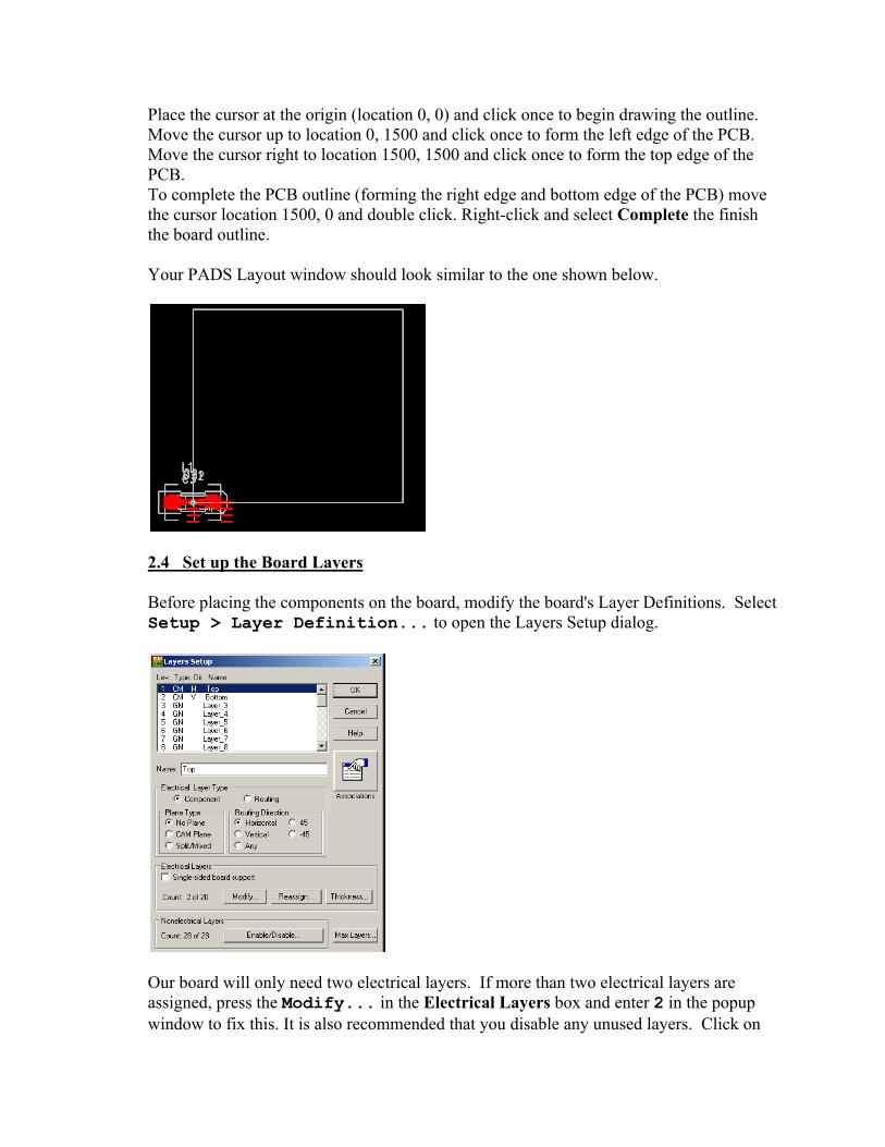
Place the cursor at the origin (location 0, 0) and click once to begin drawing the outline. Move the cursor up to location 0, 1500 and click once to form the left edge of the PCB. Move the cursor right to location 1500, 1500 and click once to form the top edge of the PCB. To complete the PCB outline (forming the right edge and bottom edge of the PCB) move the cursor location 1500, 0 and double click. Right-click and select Complete the finish the board outline. Your PADS Layout window should look similar to the one shown below.
2.4 Set up the Board Layers Before placing the components on the board, modify the board's Layer Definitions. Select Setup > Layer Definition... to open the Layers Setup dialog.
Our board will only need two electrical layers. If more than two electrical layers are assigned, press the Modify... in the Electrical Layers box and enter 2 in the popup window to fix this. It is also recommended that you disable any unused layers. Click on
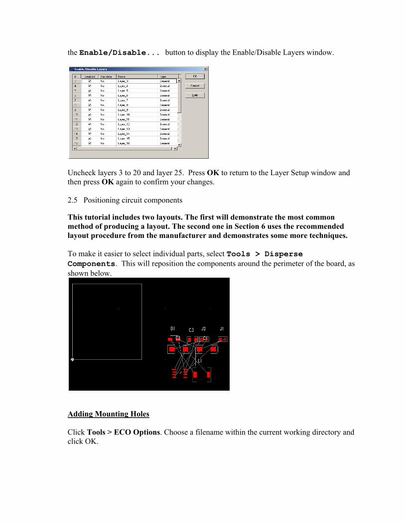
the Enable/Disable... button to display the Enable/Disable Layers window.
Uncheck layers 3 to 20 and layer 25. Press OK to return to the Layer Setup window and then press OK again to confirm your changes. 2.5 Positioning circuit components
This tutorial includes two layouts. The first will demonstrate the most common method of producing a layout. The second one in Section 6 uses the recommended layout procedure from the manufacturer and demonstrates some more techniques. To make it easier to select individual parts, select Tools > Disperse Components. This will reposition the components around the perimeter of the board, as shown below.
Adding Mounting Holes Click Tools > ECO Options. Choose a filename within the current working directory and click OK.

The ECO toolbar appears:
Click the Add Component button, , and search for *HOLE* as shown in the Get Part Type from Library window as shown.
Place the mounting holes in the layout and click OK. Examine its attributes by highlighting it, right-clicking and selecting Properties. The Pin Properties window pops up. Click the Pad Stack button to bring up the Pad Stacks Properties window. Note the Drill size and Diameter settings are set to 100 mils. You will need to know the diameter of your mounting hardware to check this size. In the case of a 4-40 screw, a good clearance diameter is 125 mils as measured by calipers. Change the Diameter and Drill size settings to 125.
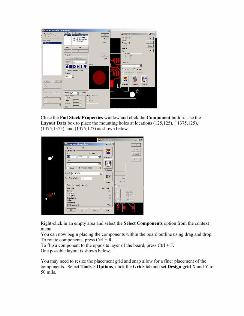
Close the Pad Stack Properties window and click the Component button. Use the Layout Data box to place the mounting holes at locations (125,125), ( 1375,125), (1375,1375), and (1375,125) as shown below.
Right-click in an empty area and select the Select Components option from the context menu. You can now begin placing the components within the board outline using drag and drop. To rotate components, press Ctrl + R. To flip a component to the opposite layer of the board, press Ctrl + F. One possible layout is shown below.
You may need to resize the placement grid and snap allow for a finer placement of the components. Select Tools > Options, click the Grids tab and set Design grid X and Y to 50 mils.

2.6 Position the Reference Designators Reposition the reference designators for your design so that they fall within the PCB outline. Right-click and choose Select Documentation from the context menu. You can now click and drag the reference designators to reposition them as shown below. Refine the design grid if necessary as demonstrated above.
Select File > Save and save the file to your PADS directory. Close PADS Layout and restore the PADS Logic window. Close the PADS Layout Link window if it is still open.
3. Routing your design using PADS Router You will now connect PADS Logic to PADS Router in the same way that you connected

to PADS Layout. Select Tools > PADS Router. The Connect to PADS Router window will appear.
Since we already have a PCB file, select Open... Then browse to N:\(PADS directory)and open the PCB file created in Part 2, above. The PADS Router program should open as shown below.
3.2 View/Modify the Design Properties To view the current design properties, right-click in the workspace and select Properties from the context menu. This will open the Design Properties window shown below.

From this window you can adjust the attributes that affect your design. Select the various tabs to get an idea of all the options available. To get further information relative to the tab click the Help button. Now select the Routing tab.
From this tab you can control, among other things, the default width of your PCB's traces. In this case the measurements are in mils. Change the Minimum to 8, Recommended to 12 and the Maximum to 20. Then press OK to confirm your changes. 3.3 Use the PADS AutoRouter to route your design. We will now use the autorouter to route the PCB design. Select Tools > Autoroute > Start to begin the autoroute process. After a few seconds, the design should be fully routed as shown below.
3.4 Verify your design
NOTE: You may encounter an error message as shown below. If this occurs, go to Tools > Options, select the File tab, double-click the link next to “Strategy” and change it to C:\Program Files\MentorGraphics\9.1PADS\SDD_HOME\Settings\

Run a design check to ensure there are no routing errors with your design. Select Tools > Verify Design. The results of the test will appear in the Output Window located at the bottom of the screen as well as markers on the layout itself. Click on the round yellow markers to show the error detail. In this particular case most of the error has to do with overlapping components.
3.5 Save your design. Select File > Save and then close PADS Router, returning to PADS Logic. Close the PADS Router Link dialog if it is still open.
4. Finishing your design in PADS Layout
4.1 Re-linking PADS Logic to PADS Layout. You will now connect to PADS Layout again and complete the final steps in your design. Select Tools > PADS Layout to open the Connect to PADS Layout window. Select Open..., browse to N:\(PADS Directory) and open your PCB file. (Remember to wait several seconds if the Server Busy message pops and click Retry). PADS Layout should open, displaying your fully routed design as shown below as well as the error markers.

Since the error relates to component placement, we can eliminate them by simply adjusting the placement. Right-click in the workspace and choose Select Components from the options. Click on the component C3 and drag it away from U1 so that the PCB is similar to that below.
Click Tools > Verify Design. The Verify Design window pops up as shown below. Note that the same errors were highlighted in Router. With Clearance selected, click Start. The following message pops up, indicating that our board outline modification fixed the Clearance errors. Click OK, then Close on the Verify Design window.

Re-routing traces The traces to C3 look a little ragged. To re-route them, right-click the workspace and choose Select Traces/Pins/Unroutes. Click on the traces that you want to modify and drag them as needed so that the layout is similar to that below.
Generating PCB printed output
Go to File > CAM > Add and click on the Layers button to choose the layer you want to print from the Available: list.
Click the Add>> button to have the layer added to the Selected box.
Select the items you wish to print in the Items on Primary box. You can select the Preview button to see what will be printed. Once you have made the appropriate selections click OK.
Enter a file name in the Document Name box.
Select the Print button in the Output Device box, then click the Device Setup button and select the target printer. Click OK in the Add Document window.

Click Run button in the Define CAM Documents window, then click Yes to generate the output.
Adding Copper Pours to your PCB You will now add a copper pour to your PCB. Enable the drafting toolbar by pressing the
button. Now press the button to enter Copper Pour Mode. Move the cursor over the origin and click once to start drawing the outline of the copper pour. Move the cursor to location 0,1500 and click to draw the left edge. Move the cursor to location 1500,1500 and click to draw the top edge. Move the cursor to location 0,1500 and double click to complete the copper pour outline. The Add Drafting window should appear as shown below.
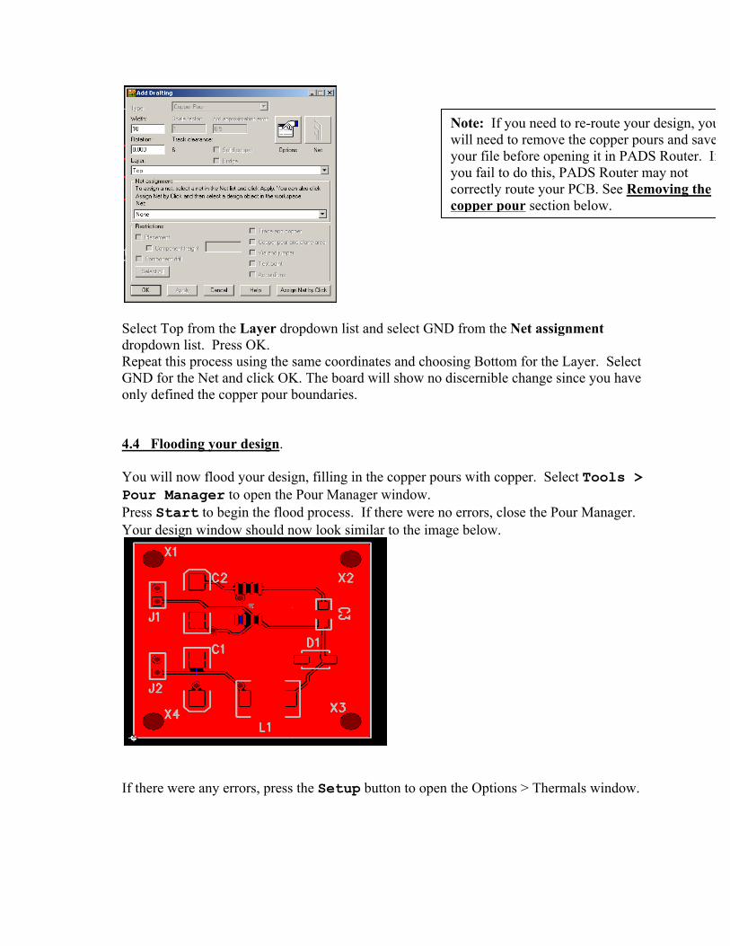
Select Top from the Layer dropdown list and select GND from the Net assignment dropdown list. Press OK. Repeat this process using the same coordinates and choosing Bottom for the Layer. Select GND for the Net and click OK. The board will show no discernible change since you have only defined the copper pour boundaries. 4.4 Flooding your design. You will now flood your design, filling in the copper pours with copper. Select Tools > Pour Manager to open the Pour Manager window. Press Start to begin the flood process. If there were no errors, close the Pour Manager. Your design window should now look similar to the image below.
If there were any errors, press the Setup button to open the Options > Thermals window.
Note: If you need to re-route your design, you will need to remove the copper pours and save your file before opening it in PADS Router. If you fail to do this, PADS Router may not correctly route your PCB. See Removing the copper pour section below.

Any copper pour errors can often be corrected by changing the type or width of the thermal spokes. Changing the type to 'Flood Over' should always prevent the 'too few spokes generated' error. This, of course, changes the method used to connect the copper pour to vias and pads of the same net. Note: Not all copper pour errors are critical, it may not be deemed necessary to modify the Thermals parameters. 4.5 Verify Design You should now check your completed design for errors. Select Tools > Verify Design to open the Verify Design window.
Select Clearance from the Check list and press start. If there are no errors, the following dialog will be displayed.
Press OK and select Connectivity from the Check list. Press Start to run the check. If there were no errors, close the window. If any errors were detected, you should locate the error image on your design and correct the problem. Save your design. Select File > Save to save your completed PCB design.
Removing the copper pour To remove the copper pour, zoom in on a portion of the copper pour outline, click to select it, right-click and select Properties and verify that the Type is Copper Pour. Click OK. Make sure the copper pour outline is still selected, then go to Edit > Delete to remove the copper pour outline, or press the Delete button.
Generating Gerber Files
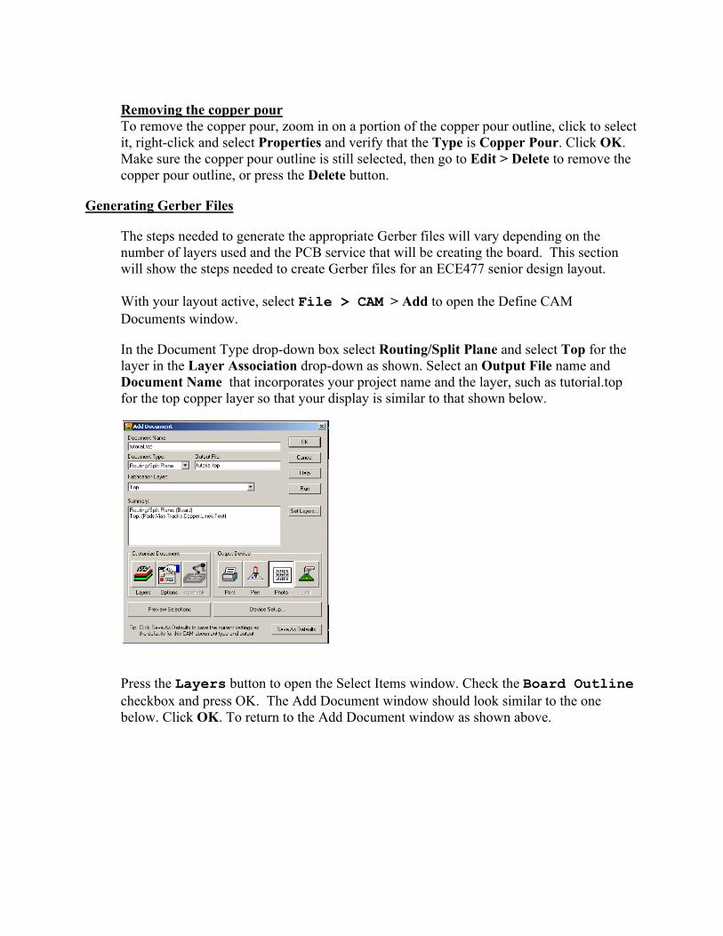
The steps needed to generate the appropriate Gerber files will vary depending on the number of layers used and the PCB service that will be creating the board. This section will show the steps needed to create Gerber files for an ECE477 senior design layout. With your layout active, select File > CAM > Add to open the Define CAM Documents window.
In the Document Type drop-down box select Routing/Split Plane and select Top for the layer in the Layer Association drop-down as shown. Select an Output File name and Document Name that incorporates your project name and the layer, such as tutorial.top for the top copper layer so that your display is similar to that shown below.
Press the Layers button to open the Select Items window. Check the Board Outline checkbox and press OK. The Add Document window should look similar to the one below. Click OK. To return to the Add Document window as shown above.
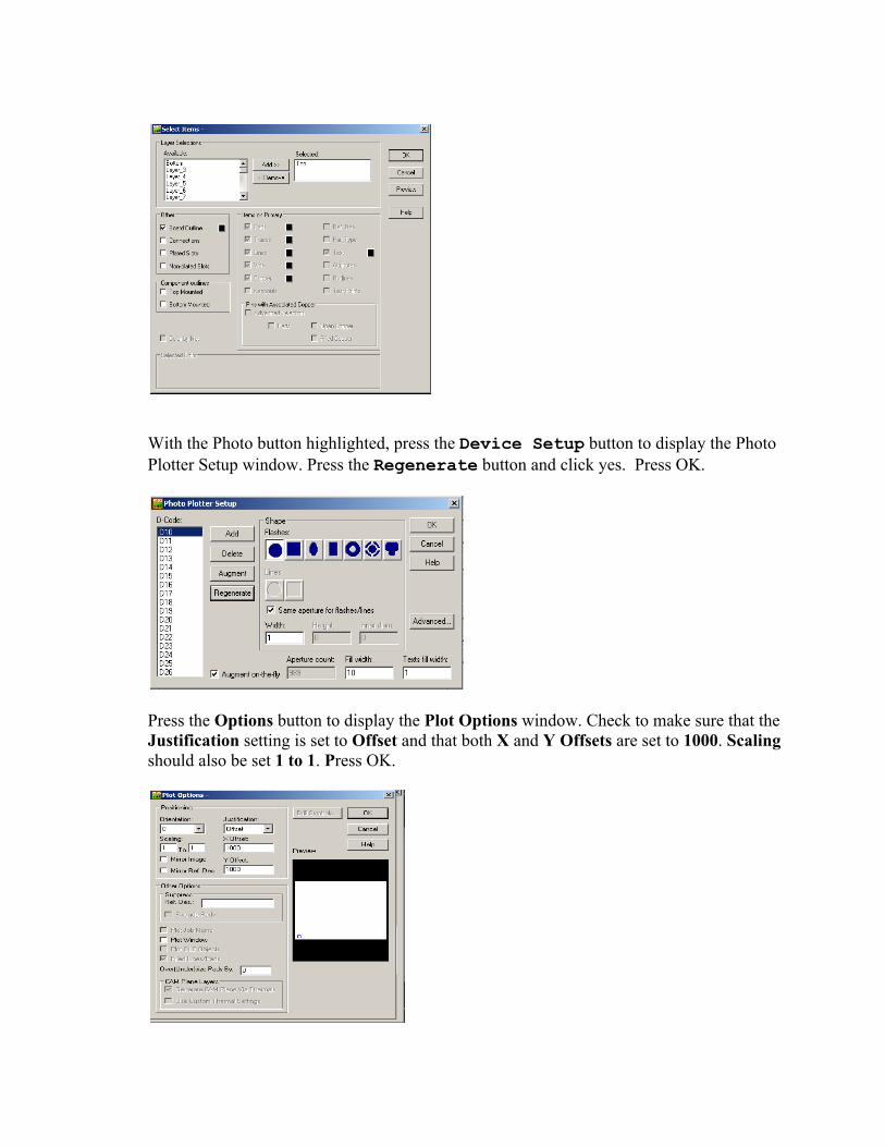
With the Photo button highlighted, press the Device Setup button to display the Photo Plotter Setup window. Press the Regenerate button and click yes. Press OK.
Press the Options button to display the Plot Options window. Check to make sure that the Justification setting is set to Offset and that both X and Y Offsets are set to 1000. Scaling should also be set 1 to 1. Press OK.

Press the Preview Selections button on the Add Document window to verify your settings. You can zoom in and out using the mouse left and right buttons respectively.
If everything looks correct, close the preview window and then press OK to add the Top document. The display should be like that shown below. Repeat the steps shown above for the bottom copper layer.
Adding the silkscreen
To add the top silkscreen click Add in the Define CAM Documents. Enter a filename such as tutorial.sst in the Document Name box. Select Silkscreen from the Document Type list and then select Top from the popup window. Press the Layers button to open the Select Items window. Select Top from the Selected List and uncheck Part Type. Press OK. Press the Options button and set the Justification to Scaling to 1 to 1. Press OK. Press the Preview Selections button to verify your design.
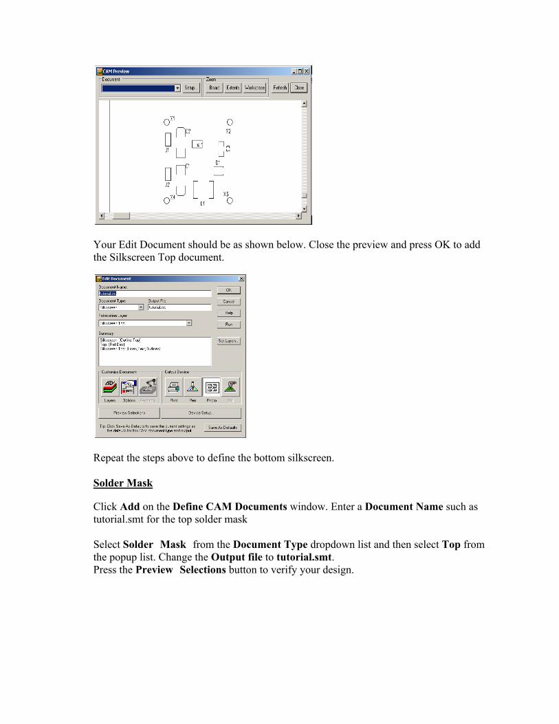
Your Edit Document should be as shown below. Close the preview and press OK to add the Silkscreen Top document.
Repeat the steps above to define the bottom silkscreen. Solder Mask
Click Add on the Define CAM Documents window. Enter a Document Name such as tutorial.smt for the top solder mask Select Solder Mask from the Document Type dropdown list and then select Top from the popup list. Change the Output file to tutorial.smt. Press the Preview Selections button to verify your design.
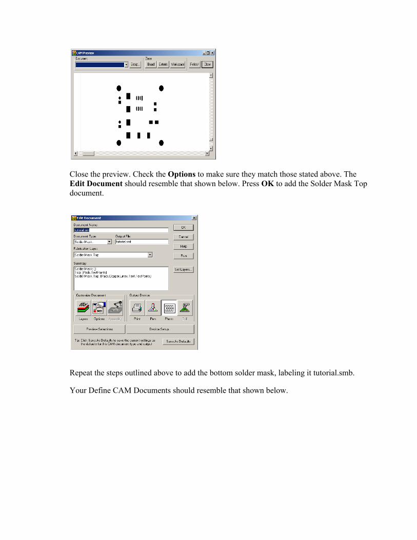
Close the preview. Check the Options to make sure they match those stated above. The Edit Document should resemble that shown below. Press OK to add the Solder Mask Top document.
Repeat the steps outlined above to add the bottom solder mask, labeling it tutorial.smb.
Your Define CAM Documents should resemble that shown below.

Drill Drawing Press Add... in the Define CAM Documents window. Type Drill Drawing for the Document Name. Select Drill Drawing from the Document Type dropdown list and then select Top from the popup list. Select Options and press the Drill Symbols button and enter 1000 for Location X and Y.
Press OK to close the Drill Drawing Options and Press OK again to return to the Add Document window. Press the Preview Selections button to verify your design.
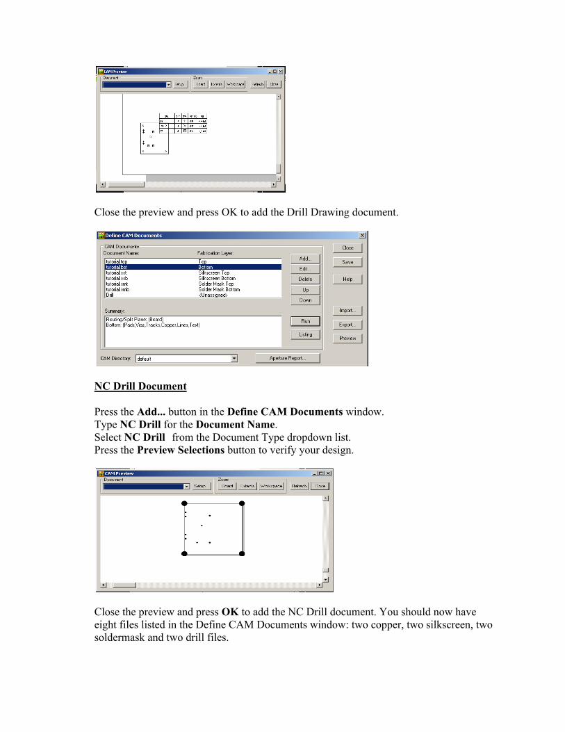
Close the preview and press OK to add the Drill Drawing document.
NC Drill Document Press the Add... button in the Define CAM Documents window. Type NC Drill for the Document Name. Select NC Drill from the Document Type dropdown list. Press the Preview Selections button to verify your design.
Close the preview and press OK to add the NC Drill document. You should now have eight files listed in the Define CAM Documents window: two copper, two silkscreen, two soldermask and two drill files.

Generate the Gerber Files Click on the CAM Directory dropdown and select <Create>. Browse to your network directory and press OK. Highlight all of the documents and press Run.
Click Yes to generate the Gerber Files. A warning may indicate a symbol size error. Ignore it. After the files have been successfully generated, press Save and then close the CAM Documents window. 5.11 Verify Gerber Files Before sending your Gerber Files to the PCB Company, it is recommended that you verify them with an external tool. PCBExpress recommends using the PentaLogix ViewMate Gerber Viewer. This requires administrator permissions to install. http://www.pentalogix.com/
This comes courtesy of bugmenot.com
Email : [email protected]

Password: 9968292
Appendix A: ALTERNATIVE LAYOUT METHOD USING MANUFACTURER’S RECOMMENDED LAYOUT
The illustration below shows a layout which approximates the one found in the data sheet for the LM2675 Simple Switcher device used in this tutorial. The data sheet is located here and the recommended layout located on page 22.
The components are first placed as shown above. Manual routing is performed by right-clicking on the workspace and choosing Select Traces/Pins. Click Setup > Design Rules > Default > Clearance and verify that Trace Width Minimum, Recommended and Maximum conform to your needs. In this case we are using 8, 12 and 20, respectively.
Click on each rubber band and route the trace so that the layout resembles that above. If the trace seems too “jumpy”, click Tools > Options > Grids and set Design grid to a finer pitch, such as 25 mils for X and Y.
To create the large and irregular copper patterns, select the Copper icon, , which enables us to draw a polygon outline which is then filled with copper. Click a starting location and draw the outline as shown below.

To finish the outline, right-click and select Complete. An Add Drafting message will pop up; click OK and observe that the outline is now filled in.
Press ESC and click on the Layout to show the new copper area in red, the top side color. This area covers the previous traces. Continue until the layout approximates the manufacturer’s recommended layout; our approximation is shown below.
Removing copper
Click on the edge of the copper that you wish to remove. With the outline highlighted, right-click, select Properties and verify that the Type is Copper. Press the Delete key to remove the copper.
Creating a ground plane
A ground plane may be used as recommended following the instructions in the data sheet noted here . Note that the data sheet states that there should be NO COPPER POUR UNDER THE INDUCTOR since the ground plane reduces the inductance.

Create the copper pour using the Copper Pour button, , to cover the bottom side of the PCB.
Select the Copper Pour Cut Out, , to produce a copper pour with cut out as shown below.
Select Tools > Pour Manager to flood the bottom side of the PCB. Your PCB should resemble that shown below which shows the bottom of the board covered with copper except for the area under the inductor.
Appendix B: Multi-Layer Layout in PADS
Some ECE477 projects, such as those utilizing FPGAs, are considerably more complex, and, as such, require multilayer boards (typically 4-layer boards are used). For this, it’s useful to know how to extend the contents of this tutorial to route on more than 2 layers.
1. Adding Electrical Layers
The first step is to designate additional layers for use as electrical layers. With your design open in PADS layout, navigate to Setup -> Layer Definition. A window should open that looks like the figure below:

In the Electrical Layers field, click Modify…. A dialog box similar to the figure below will appear.
For the purposes of this tutorial, a 4-layer design is desired. Enter 4 as the new number of electrical layers. A dialog box similar to that shown below will appear.
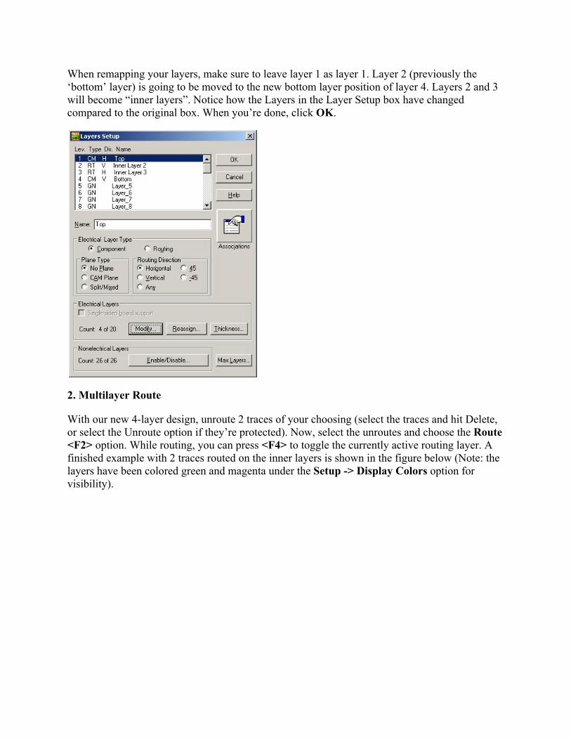
When remapping your layers, make sure to leave layer 1 as layer 1. Layer 2 (previously the ‘bottom’ layer) is going to be moved to the new bottom layer position of layer 4. Layers 2 and 3 will become “inner layers”. Notice how the Layers in the Layer Setup box have changed compared to the original box. When you’re done, click OK.
2. Multilayer Route
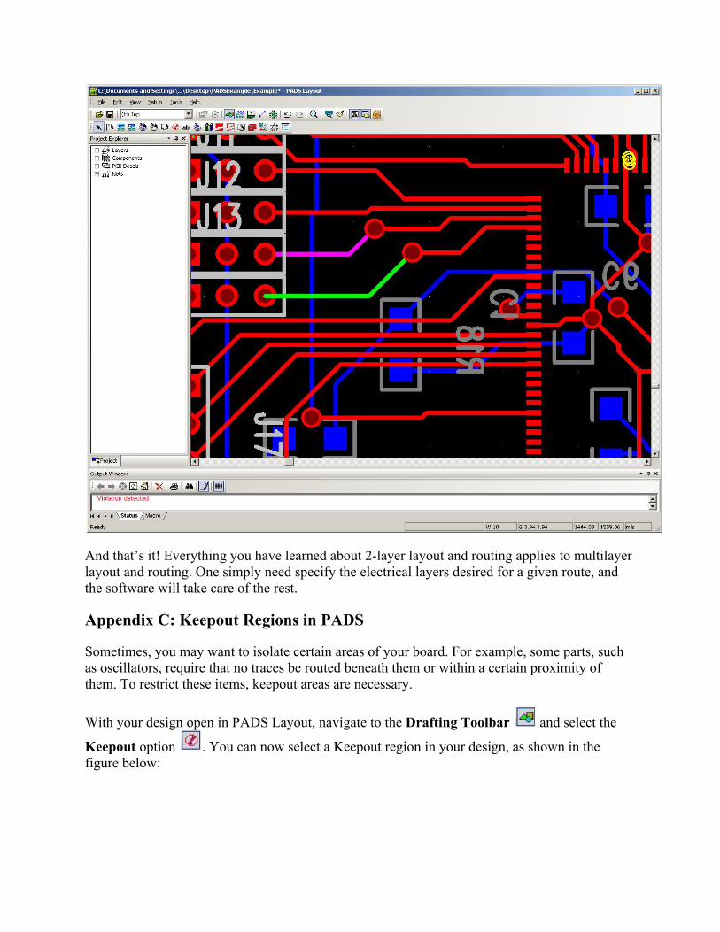
With our new 4-layer design, unroute 2 traces of your choosing (select the traces and hit Delete, or select the Unroute option if they’re protected). Now, select the unroutes and choose the Route <F2> option. While routing, you can press <F4> to toggle the currently active routing layer. A finished example with 2 traces routed on the inner layers is shown in the figure below (Note: the layers have been colored green and magenta under the Setup -> Display Colors option for visibility).
And that’s it! Everything you have learned about 2-layer layout and routing applies to multilayer layout and routing. One simply need specify the electrical layers desired for a given route, and the software will take care of the rest.
Appendix C: Keepout Regions in PADS
Sometimes, you may want to isolate certain areas of your board. For example, some parts, such as oscillators, require that no traces be routed beneath them or within a certain proximity of them. To restrict these items, keepout areas are necessary.
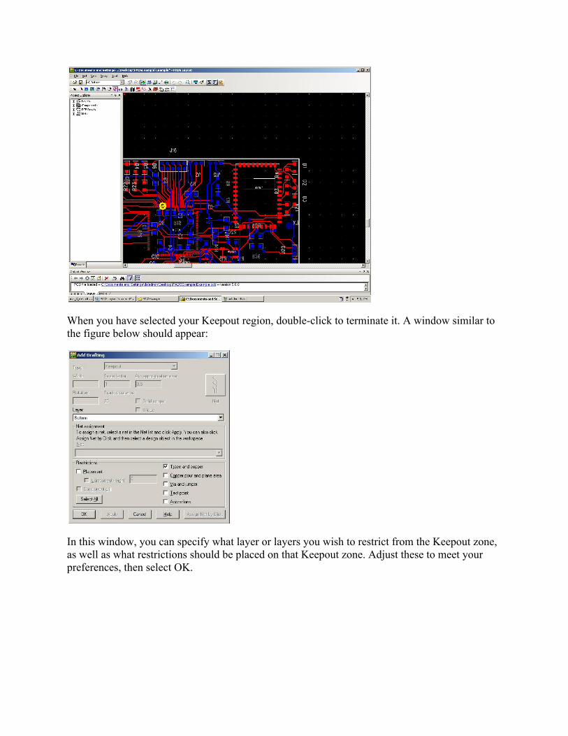
With your design open in PADS Layout, navigate to the Drafting Toolbar and select the
Keepout option . You can now select a Keepout region in your design, as shown in the figure below:
When you have selected your Keepout region, double-click to terminate it. A window similar to the figure below should appear:
In this window, you can specify what layer or layers you wish to restrict from the Keepout zone, as well as what restrictions should be placed on that Keepout zone. Adjust these to meet your preferences, then select OK.


![WPF Tutorial[Must C]-Layout-Panels-Containers & Layout Transformation](https://img.dokumen.tips/doc/110x75/577d20991a28ab4e1e934337/wpf-tutorialmust-c-layout-panels-containers-layout-transformation.jpg)


![[Cze] Tutorial Foundation Pads 2011.0](https://img.dokumen.tips/doc/110x75/577c7f971a28abe054a53f60/cze-tutorial-foundation-pads-20110.jpg)