Embed Size (px)
Citation preview

4 - 1
4.0 Hardware 4.1 Overview A CPU consists of a data section (often called a datapath) and a control section. The P8 CPU contains a simplified version of each. The datapath contains registers, an ALU, and an internal system bus. Registers are very fast memory locations that are internal to the CPU and separate from the main system memory. They can be used as “scratch pads” during calculations. The ALU is a combinational logic device that performs arithmetic and logical operations on data. The internal bus permits data exchange between the ALU and registers. The control section interprets each instruction to be executed and asserts the datapath=s control signals in the proper sequence to implement the instruction. After executing an instruction, it proceeds to the next instruction. 4.2 Design Rationale The following requirements and constraints were placed upon the hardware. In some cases they were contradictory, and a compromise was reached that favored reduced cost and/or construction time.
• It must, of course, meet the specifications outlined in Section 2.5 and implement the complete instruction set described in Section 3.7. No compromise on this point is permissible.
• Use only standard logic and memory devices. This includes
programmable devices, such as PALs and PROMs.
• To save space and wiring time, use the fewest number of IC devices that is practical.
• To reduce costs, use parts that are already on-hand whenever
possible.
• The operation of the datapath section and control section should be simple to understand, i.e., no “clever” designs that are difficult to grasp.
4 - 2
• The CPU circuitry should be separate from supporting circuitry, such as memory, I/O ports, oscillators, etc.
4.3 Programmer’s Model The programmer’s model defines the architecture of a computer. It is a high-level “machine” that is visible to the programmer, but independent of the actual physical hardware. It deals with the functional behavior of the computer as seen by the programmer. It includes the number and sizes of registers, types of instructions, addressing modes, and available memory. See Section 3 for more information on many of the architectural features of the P8 CPU. The P8 CPU consists of three 8-bit registers and one 1-bit condition register. See Figure 4.1. It is an accumulator-based design. This means that the number in the accumulator (A register) is an operand for most ALU operations. Additionally, all ALU results are placed in the A register, and overwrite its previous contents. It is also used for reading input ports and writing output ports. The R register may be used to store general data or a second operand. It also contains the memory address of operands for instructions using indirect addressing. Because the instruction pointer is an 8-bit register, only 256 bytes of memory may be addressed. Similarly, there are 256 available I/O ports, which do not share the memory space. The Z register is a 1-bit register that stores the results of the last compare operation. If the result was zero, the Z register contains a “1”, otherwise it is “0”.

4 - 3
CPU Registers +----------------+ | | Instruction Pointer (Program Counter) +----------------+ | | A Register (Accumulator) +----------------+ | | R Register (Data/Address Register) +-+--------------+ | | Z Register (Zero Flag Register) +-+ Memory Space I/O Space +----------------+ +----------------+ | | Address 00h | | | | | | | | | | | | | | | | Address FFh | | +----------------+ +----------------+
Figure 4.1: Programmer=s Model of P8 CPU.
4.4 Functional Block Model
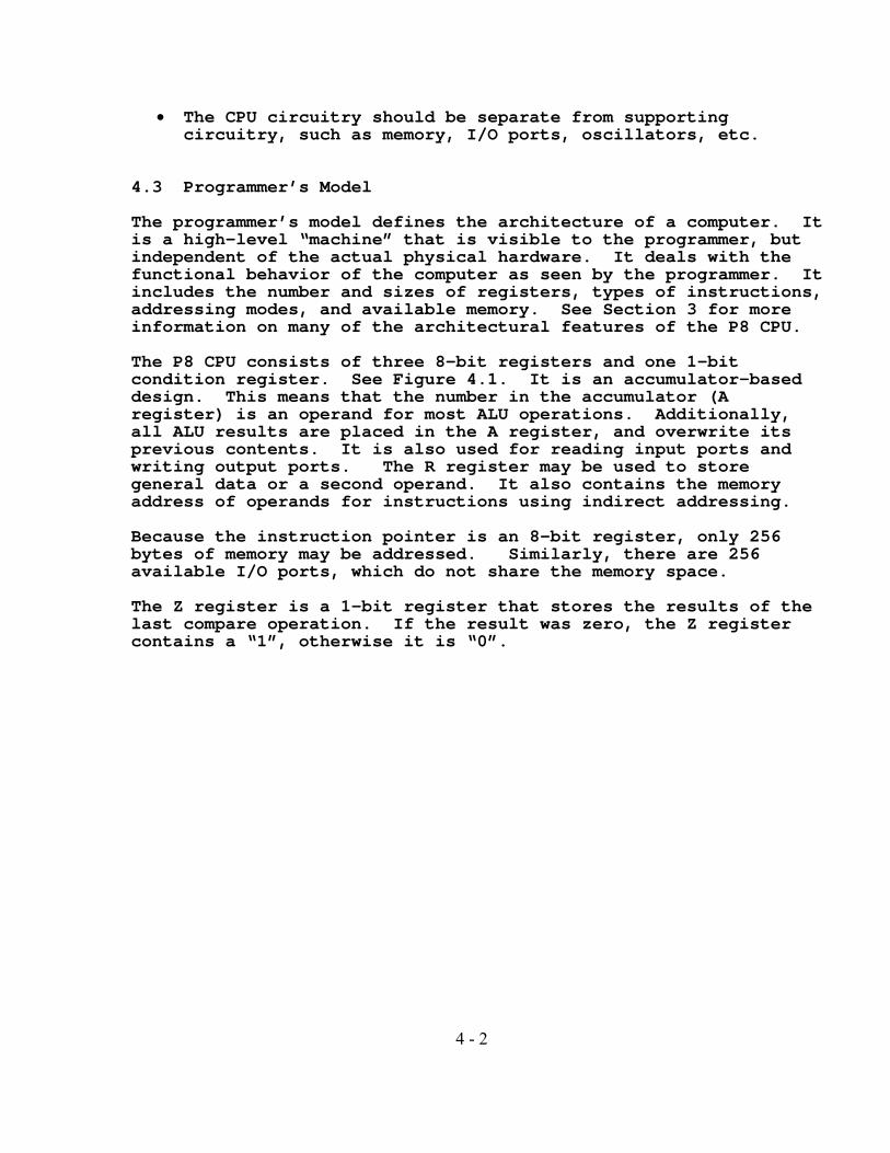
Beneath the high-level programmer=s model, are the functional units that implement it. These are the control unit, internal system busses, ALU, and registers (many of which cannot be directly manipulated users). Figure 4.2 illustrates the purposes of the CPU=s functional units and the relationships between them. These functional units implement the instruction cycle, which fetches an instruction from external memory, decodes it, reads the required operand(s), and then executes the instruction. Most instructions require several steps (microinstructions) to be performed by the CPU. The control section consists of the zero condition register (Z) and a block labeled “control logic”. The details of the control logic=s actual implementation is unimportant at this level. The diagram clearly shows, however, that it has inputs from the instruction register (IR) and Z. These inputs specify the outputs generated by the control logic. IR sends eight bits to the control unit that identify the instruction to be executed. If it is a conditional instruction, i.e., it depends on the logic level of Z, the condition bit will combine with the inputs from IR to determine the proper sequence of control signals.
4 - 4
There are two types of control logic outputs. One type is for internal use. This type consists of the datapath control bits (C0 - Cn). These control bits load registers, specify the type of ALU operation to be performed, and allow data on the internal system busses at the proper time. The other type is used by external circuitry, such as memory and I/O ports. These bits (MEMR, MEMW, IOR, IOW) control the data flow on external system busses between the CPU and its peripheral devices. The 8-bit internal bus (IB) is the primary path for data flow between the functional units. Nearly every functional unit is connected either directly, or indirectly, to IB. Using one internal system bus results in a simple hardware design that is ideal for an educational CPU. Some secondary internal busses are also present, but their connections are restricted to a small number of functional units. The ALU can perform the following operations:
• Compare • Add • Subtract • Decrement • Logical OR • Logical NOT (Invert) • Logical Shift Left
The results of most ALU operations are placed in the A register, which is the accumulator. The sole exception to this is the compare operation, which is intended only to set/reset Z. Even if an ALU result is ultimately destined for another location, it must first pass through the accumulator. The output of the accumulator is also permanently connected to one of the ALU 8-bit inputs. This means that the value in the accumulator is always an operand for ALU functions that require two operands. It is also the source for many single-operand functions. This feature allows a very simple hardware design. In fact, it is used by many commercial 8-bit microprocessors and single-chip microcontrollers for that very reason. It is, however, unsuitable for high-end CPUs because it is inefficient. The R register can be used for general data storage. Its main purpose in this CPU, however, is to illustrate two addressing modes that require an additional register. The first is register
4 - 5
addressing, where the required data are in a register. The second is indirect addressing, or in this specific case, register-indirect addressing. In this mode, the R register contains the address where the data are located. This addressing mode is implemented by transferring the contents of the R register to the operand register (OR), from which the address register (AR) is loaded. The buffer connected to the output of the A register allows the accumulator=s output to always be available to the ALU without interfering with IB. The buffer connected to the R register is actually not required for proper operation, but it was included to allow constant monitoring of the R register=s contents. This was important because of the educational nature of the CPU. The CPU accesses the external data bus with the data register (DR). DR, like the external data bus, is bi-directional. Data to be placed on the external data bus are sent to DR from either the A register or the R register along IB. Data placed in DR by the external data bus can be read by the following functional units:
• Operand Register • Instruction Register • ALU • A Register (through ALU) • R Register
The external address bus is accessed through the address register (AR). The 8-bit address in AR is placed on the external address bus. An address can be written to AR by either the instruction pointer (IP) or the operand register (OR). IP is an 8-bit binary counter that keeps track of the memory address containing the next instruction. IP increments after each instruction is read, and therefore contains the address of the instruction in the next sequential memory location. IP can also be preset to any 8-bit address placed on IB when a branch instruction is executed. OR is loaded with the memory address, or I/O port address, of required data when an instruction using direct addressing, or indirect addressing, is executed.

4 - 6
8-Bit Internal Bus | +----+ | | DR | Ext Data Bus +---/-------------------------------------> |OUT |---/---+--/--> | 8 | | 8 | 8 | +----+ | | +----+ | | | DR | | |<--------------------------------------/-- | IN |<---/--+ | 8 | | 8 | +----+ | +----+ +----+ | | IP | | AR | Ext Adr Bus +---/-------------> | |---/-----+---/--->| |---/---------> | 8 | | 8 | 8 | | 8 | +----+ | +----+ | +----+ | | | OR | | +---/-------------> | |---/-----+ | 8 | | 8 | +----+ | +----+ +----------+ | | IR | | |--> C0 +---/-------------> | |---/------------->| CONTROL | : | 8 | | 8 | LOGIC | : | +----+ | |--> CN | +----+ | |--> MEMR | | Z | | |--> MEMW | +-/->| |--/->| |--> IOR | | 1 | | 1 | |--> IOW | +----+ | +----+ +----------+ +---/-------------> | ALU|--+ | 8 | | | +-->| |---/---+ DEFINITIONS: | | +----+ 8 | | +----+ /8 +----+ | DR: Data Register | | BUF| | | A | | AR: Address Register |<-/--| |<-/-+-/-| |<------+ IP: Instruction Pointer | 8 | | 8 8 | | OR: Operand Register | +----+ +----+ IR: Instruction Register | +----+ +----+ ALU: Arithmetic Logic Unit | | BUF| | R | Z: Zero (Condition Bit) Register |<-/--| |<--/--- | |<------+ A: A Register (Accumulator) | 8 | | 8 | | | R: R Register | +----+ +----+ | BUF: 3-State Buffer +---/----------------------------+ C0-CN: Register Control Bits 8 MEMR: Memory Read Control Bit MEMW: Memory Write Control Bit IOR: IO Read Control Bit IOW: IO Write Control Bit
/8: 8-Bit Parallel Bus /1: 1-Bit Line
Figure 4.2: Functional Block Diagram of P8 CPU
4 - 7
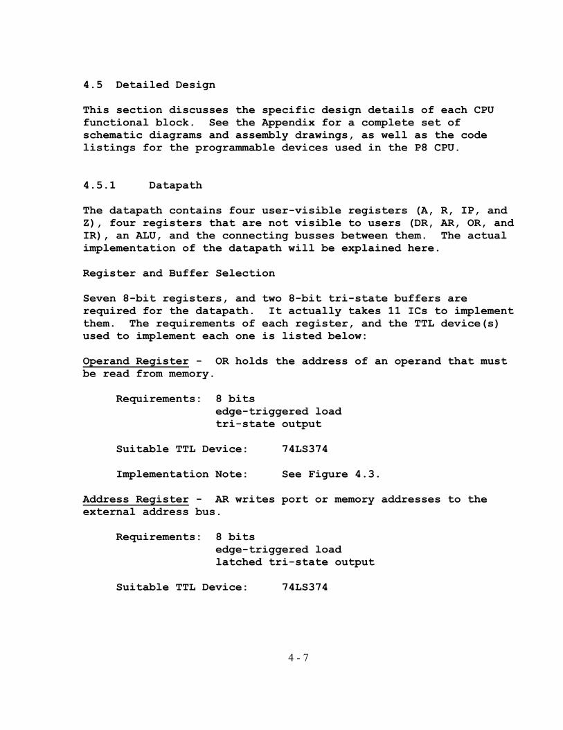
4.5 Detailed Design This section discusses the specific design details of each CPU functional block. See the Appendix for a complete set of schematic diagrams and assembly drawings, as well as the code listings for the programmable devices used in the P8 CPU. 4.5.1 Datapath The datapath contains four user-visible registers (A, R, IP, and Z), four registers that are not visible to users (DR, AR, OR, and IR), an ALU, and the connecting busses between them. The actual implementation of the datapath will be explained here. Register and Buffer Selection Seven 8-bit registers, and two 8-bit tri-state buffers are required for the datapath. It actually takes 11 ICs to implement them. The requirements of each register, and the TTL device(s) used to implement each one is listed below: Operand Register - OR holds the address of an operand that must be read from memory. Requirements: 8 bits edge-triggered load tri-state output Suitable TTL Device: 74LS374 Implementation Note: See Figure 4.3. Address Register - AR writes port or memory addresses to the external address bus. Requirements: 8 bits edge-triggered load latched tri-state output Suitable TTL Device: 74LS374
4 - 8
Implementation Notes: Latch output enable control to achieve latched tri-state output. See Figure 4.3.
Data Register - DR is a bi-directional register that writes data to the external data bus. It also reads data from the external data bus. Requirements: 8 bits bi-directional edge-triggered load tri-state output to internal bus latched tri-state output to external bus Suitable TTL Device: 74LS374 (2 required) Implementation Notes: Use 2 uni-directional registers,
DR(IN) and DR(OUT). Latch output enable control to achieve latched tri-state output. See Figure 4.3.
Instruction Pointer - IP keeps track of the next instruction to be read from memory. Requirements: 8 bits edge-triggered load edge-triggered increment clear tri-state output Suitable TTL Device: 74LS163 (2 required) Implementation Notes: Use 2 4-bit binary counters. These
counters meet all of the requirements except for the tri-state outputs. Use a single 74LS244 to buffer the eight IP output bits. See Figure 4.3.
4 - 9
Figure 4.3: Schematic of Datapath with Operand Register, Address
Register, Data Register, and Instruction Pointer

4 - 10
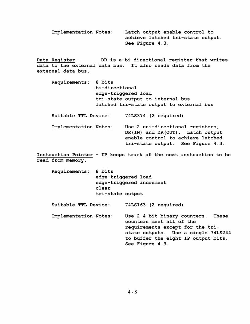
A Register - The A register is the accumulator. It is the destination for all ALU results. It is also a source for all 2-operand instructions, and many 1-operand instructions. Requirements: 8 bits edge-triggered load Suitable TTL Device: 74LS374 Implementation Notes: Permanently enable the tri-state
outputs. A 74LS273 could also have been used. The A register is isolated from IB with a 74LS244 (8-bit, tri-state buffer). This allows the outputs of the A register to be continuous inputs to the ALU. See Figure 4.4.
R Register - The R register can be used to store data, hold an ALU operand, or point an operand when using the indirect addressing mode. Requirements: 8 bits edge-triggered load Suitable TTL Device: 74LS374 Implementation Notes: See AImplementation Notes@ for the A
register. The separate buffer (74LS244) is only required to monitor the contents of the R register. See Figure 4.4.
Instruction Register - IR contains the op code of the current instruction. Its outputs are connected to the control store address bits. Requirements: 8 bits edge-triggered load synchronous clear Suitable TTL Device: 74LS273 Implementation Note: See Figure 4.4.
4 - 11
Figure 4.4: Schematic Diagram of Datapath with A Register, R Register, Instruction Register, Z Register, and ALU
4 - 12
Arithmetic Logic Unit Selection One 8-bit ALU is needed to implement the arithmetic and logical instructions. Actually, the decision of which ALU instructions to include in the instruction set was dictated by the only TTL ALU available -- the 74181. Because this is a 4-bit ALU, two of them are required. See Figure 4.4. This ALU can generate condition bits for carry, half-carry, A=B (or zero), A>B, and A<B. Only the zero condition bit is implemented in the MP8 CPU. This is sufficient to show how conditional branching works. The “A=B” output is open collector, and must be tied to an external resistor. It goes high when the A and B inputs are the same during the execution of an P8 compare instruction. (The compare instruction is actually an ALU subtract operation, but the results are not placed in the A Register.) The “CN+4” output of the least significant 4-bit ALU must be connected to the “CN” input of the most significant 4-bit ALU to create an 8-bit ALU. This connection allows a carry between bit 3 (MSB of first ALU) and bit 4 (LSB of second ALU) and generates the correct 8-bit result during an ALU operation. “CN” of the least significant ALU must be low for a subtract operation and high for all others. This input, as well as the select and mode inputs, are asserted by the control logic of the CPU. The control logic properly configures all inputs for the desired ALU operation. 4.5.2 Control Logic The control logic accepts inputs from IR and the ALU (through Z) and generates as output all the control signals necessary for the correct operation of the datapath. There are two approaches that can be taken in designing the control logic: 1) hardwired control, and 2) microcoded control. A hardwired controller is a state machine with flip flops to maintain state information and combinational logic at the inputs and outputs. Control outputs are generated for each state by the combinational output logic. The input logic combines the input bits with the present state bits to determine the next state. State transitions, and their corresponding control outputs, are synchronized by a system clock. A microcode controller consists of a microprogram in a control store memory (usually ROM) that is executed by a simple

4 - 13
microprogram address sequencer. The microprogram is composed of microwords, which are simply the data bits in each memory location. Each microword can perform one or more microinstructions, which comprise each of the P8 instructions. As each microprogram step is addressed, the data bits of the microword for that step are asserted. They are connected to a pipeline register (flip flops) where they are synchronized with the system clock. The synchronized outputs of the pipeline register are used to control the datapath and are called control bits. Each type of controller has advantages and disadvantages (Heuring & Jordan, 1997, p. 244):
• Speed: Hardwired control is much faster. It has a latency of just a few gate delays, considerably less than microcoded control units, which must perform a memory fetch for each control step.
• Ease of prototyping: The microcode design approach wins here,
since it is generally easier to reprogram a memory chip than to rewire logic.
• Flexibility of use: Once again, microcoding is superior when
the designer wishes to change instruction sets. This might be desirable for instruction set upgrades or when several instruction sets are to be emulated.
Microprogrammed control was selected for this CPU because it is simpler to implement, and more easily modified than hardwired control. It is slower than hardwired control, but that is not a serious disadvantage for the P8 CPU. Control Store Configuration Thirty-one control signals are required to operate the P8 CPU. Because industry-standard PROMs are 8 bits wide, four of them are used to create the control store with a 32-bit microword. This leaves one control bit (C29) unused. The control store PROMS need 12 address bits. Eight are used by the opcode of the instruction to be executed, three are needed to address the individual microwords (up to 8) that comprise each instruction, and one bit is used to determine the action of conditional instructions. The 2732 (4K X 8) PROM would have been ideal for this application, but none were available. The 2764 (8K X 8) PROM was substituted. The
4 - 14
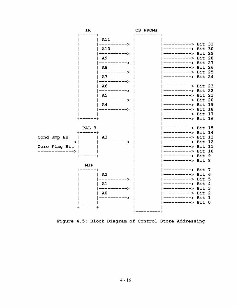
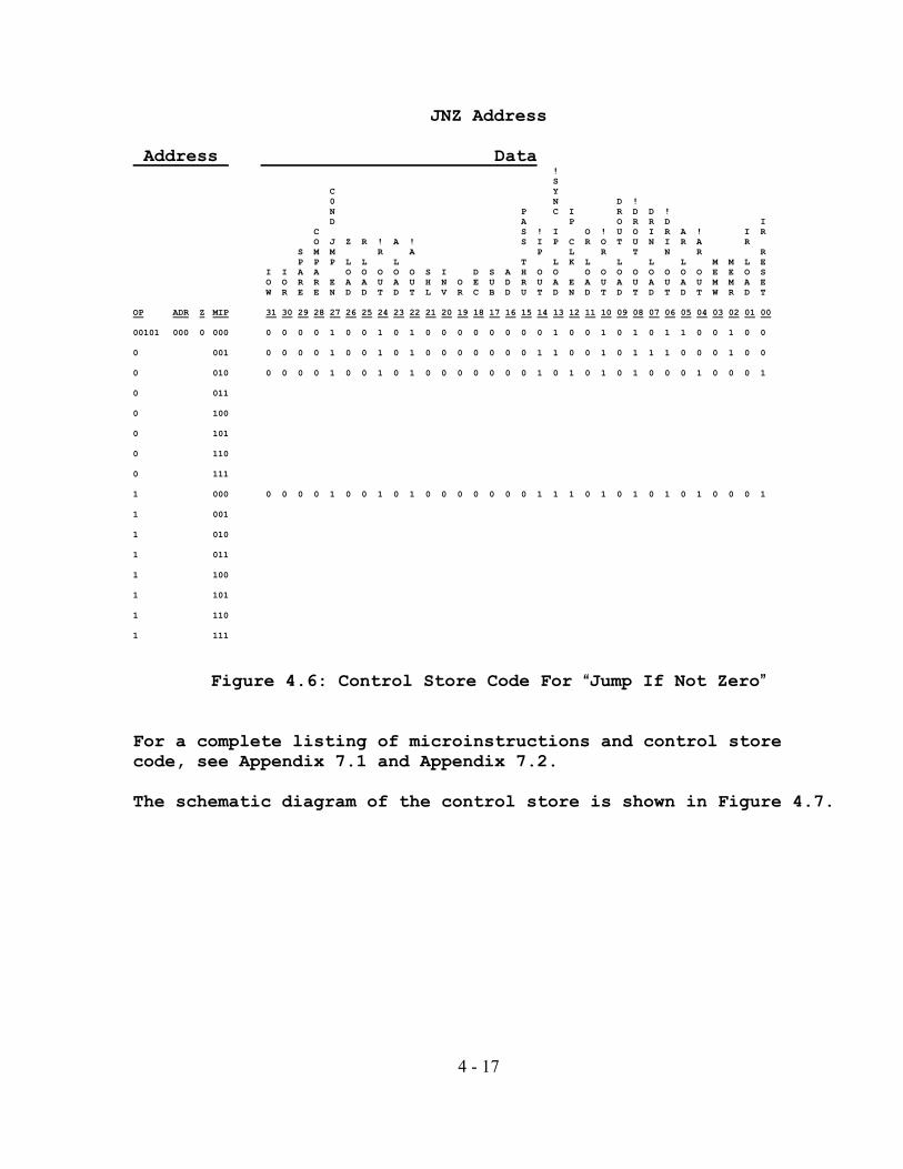
most significant address bits of the 2764 PROMs are disabled by grounding them. These PROMs are not used very efficiently for this application, but at the board level, the amount of wasted silicon area is not important. Each P8 instruction is assigned a block of 16 consecutive addresses within the control store. See Figure 4.5 for a block diagram of how the control store is addressed. Each instruction=s block is selected with its 8-bit opcode, which is connected to the eight most significant control store address bits. Address bit 3 is connected via some enabling logic in PAL 3 to the condition bit register (Z). This divides the instruction=s control store block into two sub-blocks of eight addresses each. Most instructions use only the first sub-block (A3 = 0). Conditional instructions, however, have microwords coded into both sub-blocks. The value of the condition bit, and, therefore, A3, determines which set of microwords will be executed. This allows the same instruction to execute differently for each value in Z. The three least significant control store address bits are connected to a binary counter called the microinstruction pointer (MIP). This counter sequences through each of the microwords that contain microinstructions required to execute the instruction in IR. Figure 4.6 shows the control store code that implements the “Jump If Not Zero” Instruction. The 5-bit operation and 3-bit addressing mode fields of the 8-bit opcode (28h) are combined with the condition bit (Z) and the 3-bit MIP output to form the 12-bit control store address. If the condition bit is not set (Z = 0) the jump is executed. It takes three microwords, which encode a total of eight microinstructions, to complete. If Z = 1, the jump is not executed, and the only microinstruction necessary is to reset IR. The purpose of each of the 31 control bits is clearly labeled in Figure 4.6. They can be traced to the various registers in the schematic diagram.
4 - 15
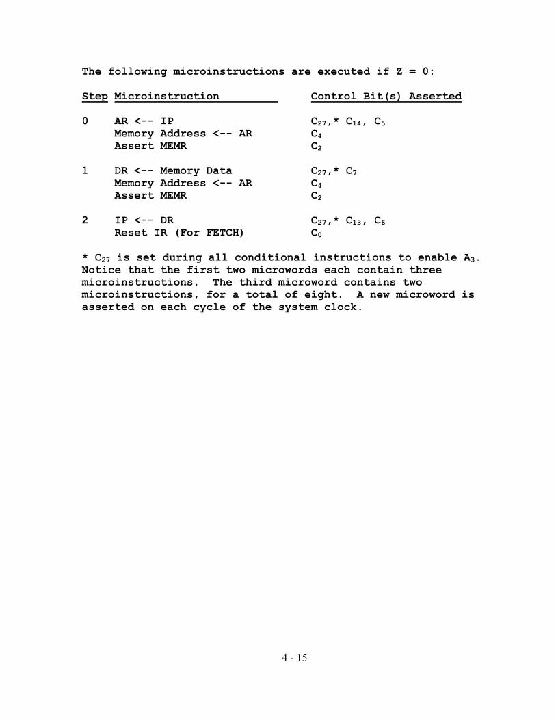
The following microinstructions are executed if Z = 0: Step Microinstruction Control Bit(s) Asserted 0 AR <-- IP C27,* C14, C5 Memory Address <-- AR C4 Assert MEMR C2 1 DR <-- Memory Data C27,* C7 Memory Address <-- AR C4 Assert MEMR C2 2 IP <-- DR C27,* C13, C6 Reset IR (For FETCH) C0 * C27 is set during all conditional instructions to enable A3. Notice that the first two microwords each contain three microinstructions. The third microword contains two microinstructions, for a total of eight. A new microword is asserted on each cycle of the system clock.
4 - 16
IR CS PROMs +------+ +---------+
| | A11 | | | |----------> | |----------> Bit 31
| | A10 | |----------> Bit 30 | |----------> | |----------> Bit 29 | | A9 | |----------> Bit 28 | |----------> | |----------> Bit 27 | | A8 | |----------> Bit 26 | |----------> | |----------> Bit 25 | | A7 | |----------> Bit 24 | |----------> | | | | A6 | |----------> Bit 23 | |----------> | |----------> Bit 22 | | A5 | |----------> Bit 21 | |----------> | |----------> Bit 20 | | A4 | |----------> Bit 19 | |----------> | |----------> Bit 18 | | | |----------> Bit 17 +------+ | |----------> Bit 16 | | PAL 3 | |----------> Bit 15 +------+ | |----------> Bit 14 Cond Jmp En | | A3 | |----------> Bit 13 ------------->| |----------> | |----------> Bit 12 Zero Flag Bit | | | |----------> Bit 11 ------------->| | | |----------> Bit 10 +------+ | |----------> Bit 9 | |----------> Bit 8 MIP | | +------+ | |----------> Bit 7 | | A2 | |----------> Bit 6 | |----------> | |----------> Bit 5 | | A1 | |----------> Bit 4 | |----------> | |----------> Bit 3 | | A0 | |----------> Bit 2 | |----------> | |----------> Bit 1 | | | |----------> Bit 0 +------+ | | +---------+
Figure 4.5: Block Diagram of Control Store Addressing
4 - 17
JNZ Address Address Data ! S C Y 0 N D ! N P C I R D D ! D A P O R R D I C S ! I O ! U O I R A ! I R O J Z R ! A ! S I P C R O T U N I R A R S M M R A P L R T N R R P P P L L L T L K L L L L M M L E I I A A O O O O O S I D S A H O O O O O O O O O O E E O S O O R R E A A U A U H N O E U D R U A E A U A U A U A U M M A E W R E E N D D T D T L V R C B D U T D N D T D T D T D T W R D T OP ADR Z MIP 31 30 29 28 27 26 25 24 23 22 21 20 19 18 17 16 15 14 13 12 11 10 09 08 07 06 05 04 03 02 01 00 00101 000 0 000 0 0 0 0 1 0 0 1 0 1 0 0 0 0 0 0 0 0 1 0 0 1 0 1 0 1 1 0 0 1 0 0 0 001 0 0 0 0 1 0 0 1 0 1 0 0 0 0 0 0 0 1 1 0 0 1 0 1 1 1 0 0 0 1 0 0 0 010 0 0 0 0 1 0 0 1 0 1 0 0 0 0 0 0 0 1 0 1 0 1 0 1 0 0 0 1 0 0 0 1 0 011 0 100 0 101 0 110 0 111 1 000 0 0 0 0 1 0 0 1 0 1 0 0 0 0 0 0 0 1 1 1 0 1 0 1 0 1 0 1 0 0 0 1 1 001 1 010 1 011 1 100 1 101 1 110 1 111
Figure 4.6: Control Store Code For AJump If Not Zero@
For a complete listing of microinstructions and control store code, see Appendix 7.1 and Appendix 7.2. The schematic diagram of the control store is shown in Figure 4.7.

4 - 18
Figure 4.7: Schematic Diagram of Control Store
4 - 19
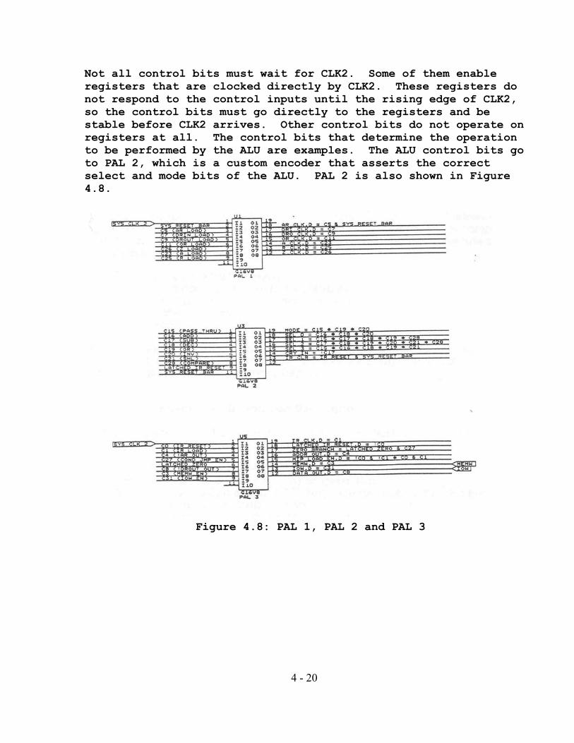
Control Store Sequencer The control store sequencer, or microinstruction pointer (MIP), is a 74LS163. It is a 4-bit counter with a synchronous load, synchronous reset, and positive edge triggering. Its purpose is to step through the consecutive microwords for each P8 instruction that executes. Only three of its four bits are used, because no instruction has more than eight microwords. The three least significant outputs of the MIP are connected to the three least significant address bits of the control store PROMs. The count enables of the MIP are permanently set to count on each positive clock edge. When clocked while the system reset is asserted, the count operation is overridden and the MIP is reset to zero. This allows it to address the first microword of the FETCH operation after the reset is released. On the last microinstruction of FETCH or any P8 instruction, the load enable is asserted, which overrides the count enables and loads the MIP with zero on the next clock pulse. Control Signal Timing When the control store=s address inputs change in order to execute a different microword, all of the control store=s data bits change. It is important that these bits settle to the correct logic level before they are allowed to affect the datapath. To ensure this happens, the P8 has a 2-phase system clock. The MIP is connected to phase 1 (CLK1). The pipeline register (PAL 1 and PAL 3), and datapath are connected to phase 2 (CLK2). When CLK1 goes from low to high, the MIP increments to the next microword. The control bits of that microword are asserted, but no registers in the datapath change states until the rising edge of CLK2. Enough time elapses between the rising edge of CLK1 and the rising edge of CLK2 to allow the outputs of the control store to stabilize before they are acted upon. This is necessary because the control bits do not all assert simultaneously. Most of them are connected to the inputs of positive edge triggered flip flops in PAL 1 and PAL 3 until CLK2, which is also connected to PAL 1 and PAL 3, clocks. When CLK2 asserts, all of the register-clocking control bits are allowed through the pipeline register simultaneously so that all of the registers in the datapath change states together. Figure 4.8 shows PAL 1 and PAL 3, along with the logic equation of each output.
4 - 20
Not all control bits must wait for CLK2. Some of them enable registers that are clocked directly by CLK2. These registers do not respond to the control inputs until the rising edge of CLK2, so the control bits must go directly to the registers and be stable before CLK2 arrives. Other control bits do not operate on registers at all. The control bits that determine the operation to be performed by the ALU are examples. The ALU control bits go to PAL 2, which is a custom encoder that asserts the correct select and mode bits of the ALU. PAL 2 is also shown in Figure 4.8.
Figure 4.8: PAL 1, PAL 2 and PAL 3

4 - 21
After a system reset, the MIP contains 0h and IR contains 00h. This will execute the first microinstruction of FETCH during the next CLK2. To ensure that CLK2 is the first clock pulse after a system reset, a D flip flop is used as a reset synchronizer. See Figure 4.9.
Figure 4.9: Reset Synchronizer