Embed Size (px)
Citation preview

1SPECTROSCOPY GROUPNANOMATERIALS AND CAMBRIDGE UNIVERSITY
DEPARTMENT OF ENGINEERINGELECTRONIC DEVICES
AND MATERIALS GROUP
P5-Electromagnetic Fields and Waves
Andrea C. Ferrarihttp://www-g.eng.cam.ac.uk/nms/lecturenotes.html
1
2SPECTROSCOPY GROUPNANOMATERIALS AND CAMBRIDGE UNIVERSITY
DEPARTMENT OF ENGINEERINGELECTRONIC DEVICES
AND MATERIALS GROUP
6 Lectures3 Main Sections ~2 lectures per subject
I Transmission Lines
I.1 Telegrapher’s EquationsI.2 Characteristic ImpedanceI.3 Reflection
I.0 The wave equation
2

3SPECTROSCOPY GROUPNANOMATERIALS AND CAMBRIDGE UNIVERSITY
DEPARTMENT OF ENGINEERINGELECTRONIC DEVICES
AND MATERIALS GROUP
II Electromagnetic Waves in Free SpaceII.1 Electromagnetic FieldsII.2 Electromagnetic WavesII.3 Reflection and Refraction of Waves
III Antennae and Radio TransmissionIII.1 Antennae
III.2 Radio
3

4SPECTROSCOPY GROUPNANOMATERIALS AND CAMBRIDGE UNIVERSITY
DEPARTMENT OF ENGINEERINGELECTRONIC DEVICES
AND MATERIALS GROUP
OBJECTIVESAs the frequency of electronic circuits rises, one can no longer assume that voltages and currents are instantly transmitted by a wire.
•Appreciate when a wave theory is needed
•Derive and solve simple transmission line problems•Understand the importance of matching to the characteristic impedance of a transmission cable
•Understand basic principles of EM wave propagation in free space, across interfaces and the use of antennae
The objectives of this course are:
4

5SPECTROSCOPY GROUPNANOMATERIALS AND CAMBRIDGE UNIVERSITY
DEPARTMENT OF ENGINEERINGELECTRONIC DEVICES
AND MATERIALS GROUP
Reference: OLVER A.D. Microwave and Optical TransmissionJohn Wiley & Sons, 1992, 1997
Shelf Mark: NV 135
5

6SPECTROSCOPY GROUPNANOMATERIALS AND CAMBRIDGE UNIVERSITY
DEPARTMENT OF ENGINEERINGELECTRONIC DEVICES
AND MATERIALS GROUP
Handouts
Left-hand Column: Read if you need extra clarification
The handouts have some gaps for you to fill
In both CASES 1) and 2) You will be able to Download a PDF of these slides from
http://www-g.eng.cam.ac.uk/nms/lecturenotes.html6
1) DO NOT PANIC IF YOU DO NOT MANAGE TO WRITE DOWN IN “REAL TIME”
2) Prefer to just sit back and relax?
NOTE:
7SPECTROSCOPY GROUPNANOMATERIALS AND CAMBRIDGE UNIVERSITY
DEPARTMENT OF ENGINEERINGELECTRONIC DEVICES
AND MATERIALS GROUP
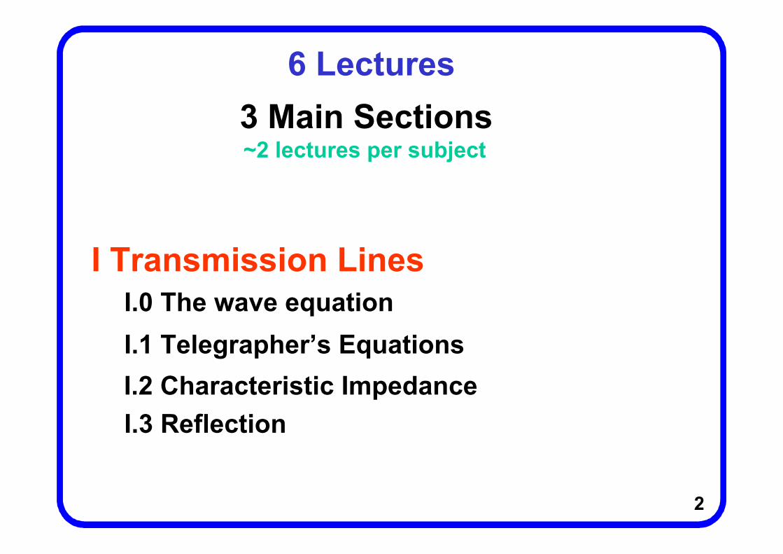
I.0 The Wave Equation
AimsTo recall basic phasors conceptsTo introduce the generalised form of the Wave Equation
ObjectivesAt the end of this section you should be able to recognisethe generalised form of the wave equation, its general solution, the propagation direction and velocity
7

8SPECTROSCOPY GROUPNANOMATERIALS AND CAMBRIDGE UNIVERSITY
DEPARTMENT OF ENGINEERINGELECTRONIC DEVICES
AND MATERIALS GROUP
I.0.0 IntroductionAn ideal transmission line is defined to be a link between two points in which the signal at any point equals the initiating signal
I.e. transmission takes place instantaneously and there is no attenuation
Real world transmission lines are not ideal, there is attenuation and there are delays in transmission
8
9SPECTROSCOPY GROUPNANOMATERIALS AND CAMBRIDGE UNIVERSITY
DEPARTMENT OF ENGINEERINGELECTRONIC DEVICES
AND MATERIALS GROUP
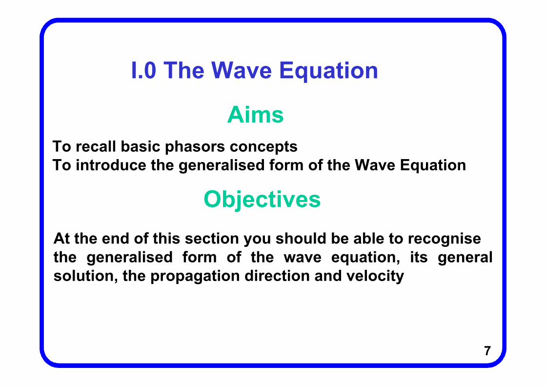
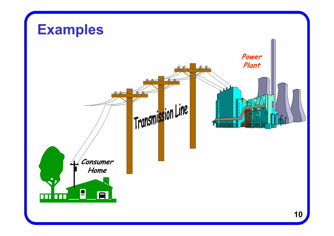
A transmission line can be seen as a device for propagating energy from one point to another
The propagation of energy is for one of two general reasons:
1. Power transfer (e.g. for lighting, heating, performing work) - examples are mains electricity, microwave guides in a microwave oven, a fibre-optic illuminator.
2. Information transfer. examples are telephone, radio, and fibre-optic links (in each case the energy propagating down the transmission line is modulated in some way).
9
10SPECTROSCOPY GROUPNANOMATERIALS AND CAMBRIDGE UNIVERSITY
DEPARTMENT OF ENGINEERINGELECTRONIC DEVICES
AND MATERIALS GROUP
PowerPlant
ConsumerHome
10
Examples

11SPECTROSCOPY GROUPNANOMATERIALS AND CAMBRIDGE UNIVERSITY
DEPARTMENT OF ENGINEERINGELECTRONIC DEVICES
AND MATERIALS GROUP 11

12SPECTROSCOPY GROUPNANOMATERIALS AND CAMBRIDGE UNIVERSITY
DEPARTMENT OF ENGINEERINGELECTRONIC DEVICES
AND MATERIALS GROUP
CoCo--axax cablecablePair of wiresPair of wires
PCB tracksPCB tracks IC interconnectsIC interconnects
12
13SPECTROSCOPY GROUPNANOMATERIALS AND CAMBRIDGE UNIVERSITY
DEPARTMENT OF ENGINEERINGELECTRONIC DEVICES
AND MATERIALS GROUP
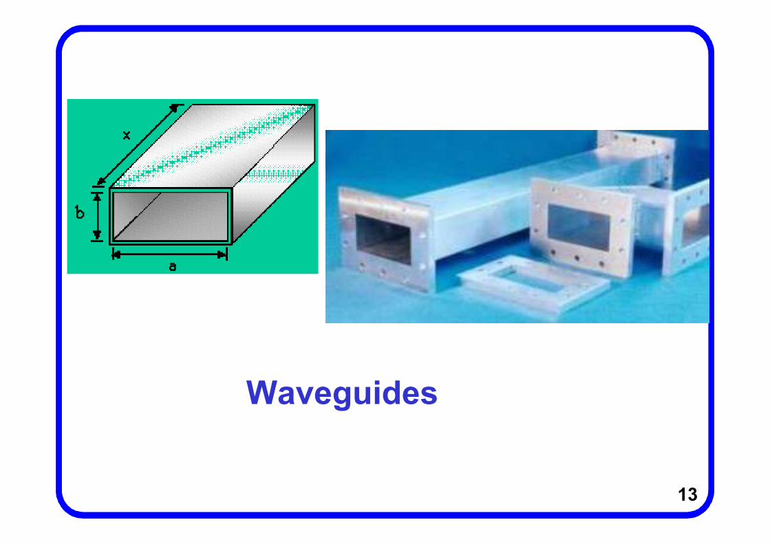
Waveguides
13

14SPECTROSCOPY GROUPNANOMATERIALS AND CAMBRIDGE UNIVERSITY
DEPARTMENT OF ENGINEERINGELECTRONIC DEVICES
AND MATERIALS GROUP
Dielectric of thickness T, with a conductor deposited on the bottom surface, and a strip of conductor of width W on the top surface
Mircostrip
Can be fabricated using Printed Circuit Board (PCB) technology, and is used to convey microwave frequency signals 14

15SPECTROSCOPY GROUPNANOMATERIALS AND CAMBRIDGE UNIVERSITY
DEPARTMENT OF ENGINEERINGELECTRONIC DEVICES
AND MATERIALS GROUP 15Microwave Oven

16SPECTROSCOPY GROUPNANOMATERIALS AND CAMBRIDGE UNIVERSITY
DEPARTMENT OF ENGINEERINGELECTRONIC DEVICES
AND MATERIALS GROUP
Optical Fibres
16
17SPECTROSCOPY GROUPNANOMATERIALS AND CAMBRIDGE UNIVERSITY
DEPARTMENT OF ENGINEERINGELECTRONIC DEVICES
AND MATERIALS GROUP
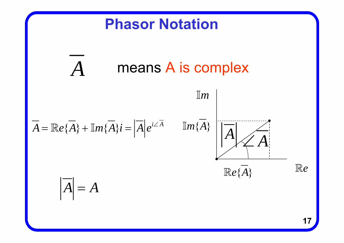
Phasor Notation
A means A is complex
{ } { } i AA e A m A i A e
A A
m
e{ }e A
AA{ }m A
17

18SPECTROSCOPY GROUPNANOMATERIALS AND CAMBRIDGE UNIVERSITY
DEPARTMENT OF ENGINEERINGELECTRONIC DEVICES
AND MATERIALS GROUP
j xAe is short-hand for ( )e j x tAe
which equals: cosA x t A
Proof
cos( ) sin( )ie j
cos( ) sin( )j x t AAe A x t A jA x t A
then
( ) ( ) ( )j x t j A j x t j x t AAe Ae e Ae
18

19SPECTROSCOPY GROUPNANOMATERIALS AND CAMBRIDGE UNIVERSITY
DEPARTMENT OF ENGINEERINGELECTRONIC DEVICES
AND MATERIALS GROUP
I.0.1 The Wave EquationThe generalised form of the wave equation is:
22 2
2
A v At
Where the Laplacian of a scalar A is:
2 2 22
2 2 2
A A AAx y z
19

20SPECTROSCOPY GROUPNANOMATERIALS AND CAMBRIDGE UNIVERSITY
DEPARTMENT OF ENGINEERINGELECTRONIC DEVICES
AND MATERIALS GROUP
We will be looking at plane waves for which the wave equation is one-dimensional and appears as follows:
2 22
2 2
A Avt x
Where A could be:
Either the Voltage (V) or the Current (I)as in waves in a transmission line
Or the Electric Field (E) or Magnetic Field (H)as in Electromagnetic Waves in free space
or2 2
2 2 2
1A Ax v t
20

21SPECTROSCOPY GROUPNANOMATERIALS AND CAMBRIDGE UNIVERSITY
DEPARTMENT OF ENGINEERINGELECTRONIC DEVICES
AND MATERIALS GROUP
The constant v is called the wave speed, from the general solution to the wave equation:
( )A f x vt
Note
( )A f x vt Forward moving
( )A f x vt Backward moving 21

22SPECTROSCOPY GROUPNANOMATERIALS AND CAMBRIDGE UNIVERSITY
DEPARTMENT OF ENGINEERINGELECTRONIC DEVICES
AND MATERIALS GROUP
ΔΔxx
xx
ΔΔxx
t+t+ΔΔt tt t
F(t+x/vF(t+x/v))
xx
If t increases (t→t+∆t), x must also increase if x-vt is to be constant
Direction of travel
Consider a fixed point, P, on the moving waveform, i.e. a point with constant f
x increases implies wave is moving to right (Forward)
f(x-vt) will be constant if x-vt is constant
PPt t+t t+ΔΔtt
Similarly, for x+vt wave is moving to left (Backward)
( )f x vt( )f x vt
22

23SPECTROSCOPY GROUPNANOMATERIALS AND CAMBRIDGE UNIVERSITY
DEPARTMENT OF ENGINEERINGELECTRONIC DEVICES
AND MATERIALS GROUP
Proof f is general solution
( )A f x vt
'( )A vf x vtt
22
2 ''( )A v f x vtt
'( )A f x vtx
2
2 ''( )A f x vtx
2 22
2 2
A Avt x
23

24SPECTROSCOPY GROUPNANOMATERIALS AND CAMBRIDGE UNIVERSITY
DEPARTMENT OF ENGINEERINGELECTRONIC DEVICES
AND MATERIALS GROUP
I.1 Electrical Waves
AimsTo derive the telegrapher’s equationTo account for losses in transmission lines
ObjectivesAt the end of this section you should be able to recognisewhen the wave theory is relevant. To master the concepts of wavelenght, wave velocity, period and phase. To describe the propagation of waves in loss-less and lossytransmission lines
24

25SPECTROSCOPY GROUPNANOMATERIALS AND CAMBRIDGE UNIVERSITY
DEPARTMENT OF ENGINEERINGELECTRONIC DEVICES
AND MATERIALS GROUP
L
I.1.1 Telegrapher’s EquationsLet us consider a short length of a wire pairLet us define
series/loop inductance per unit length [H/m]
LV
I
LIV L xt
x
L x
25

26SPECTROSCOPY GROUPNANOMATERIALS AND CAMBRIDGE UNIVERSITY
DEPARTMENT OF ENGINEERINGELECTRONIC DEVICES
AND MATERIALS GROUP
C parallel/shunt capacitance per unit length [F/m]
CI
CC
VI C xt
CV
x
C x
26

27SPECTROSCOPY GROUPNANOMATERIALS AND CAMBRIDGE UNIVERSITY
DEPARTMENT OF ENGINEERINGELECTRONIC DEVICES
AND MATERIALS GROUP
C LV V V
FII I xx
x
CVV V xx
CC
VI C xt
LIV L xt
I
CII xx
CVLV
A
27

28SPECTROSCOPY GROUPNANOMATERIALS AND CAMBRIDGE UNIVERSITY
DEPARTMENT OF ENGINEERINGELECTRONIC DEVICES
AND MATERIALS GROUP
C LV V V V IV x V L xx t
F CI I I I VI x I C xx t
V ILx t
I VCx t
(1.1)
(1.2)
28

29SPECTROSCOPY GROUPNANOMATERIALS AND CAMBRIDGE UNIVERSITY
DEPARTMENT OF ENGINEERINGELECTRONIC DEVICES
AND MATERIALS GROUP
I.1.2 Travelling Wave Equations
2
2
V Lx t
Ix
Ix
2
2
I Cx t
Vx
(1.1a)
(1.2a)
Then in (1.1a) substitute
Let us differentiate both (1.1) and (1.2) with respect to x
using (1.2)
Then in (1.2a) substitute Vx
2
2
VLCt
2
2
ILCt
using (1.1)29
30SPECTROSCOPY GROUPNANOMATERIALS AND CAMBRIDGE UNIVERSITY
DEPARTMENT OF ENGINEERINGELECTRONIC DEVICES
AND MATERIALS GROUP
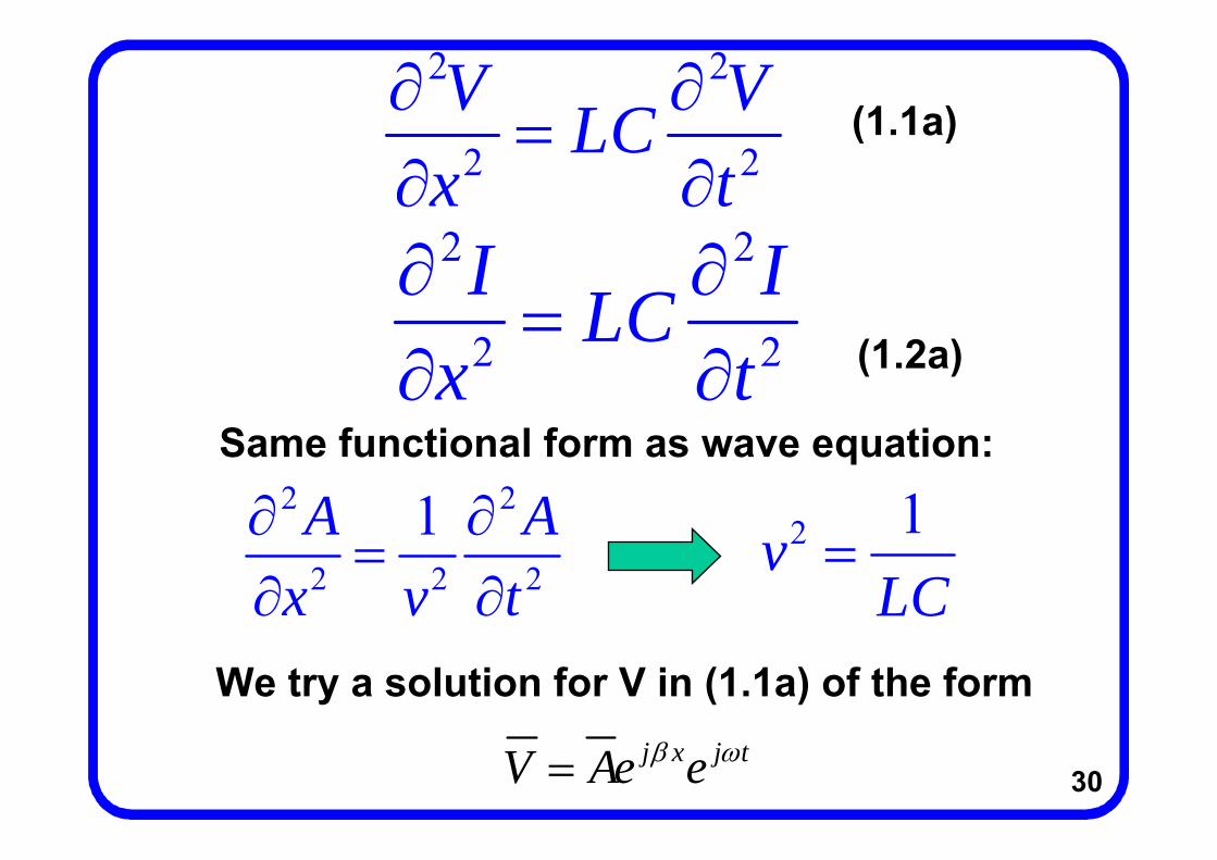
2 2
2 2
V VLCx t
2 2
2 2 2
1A Ax v t
2 2
2 2
I ILCx t
(1.1a)
(1.2a)
Same functional form as wave equation:
We try a solution for V in (1.1a) of the formj x j tV Ae e
2 1vLC
30

31SPECTROSCOPY GROUPNANOMATERIALS AND CAMBRIDGE UNIVERSITY
DEPARTMENT OF ENGINEERINGELECTRONIC DEVICES
AND MATERIALS GROUP
2 2j x j t j x j tAe e LC Ae e
LC
j x j x j tF BV e V e V e e
j x j x j tF BI e I e I e e
Hence
Phase Constant (1.3)
Since β can be positive of negative we obtain expressions for voltage and current waves moving forward (subscript F) and backward (subscript B) along the transmission line
(1.4)
(1.5)
31

32SPECTROSCOPY GROUPNANOMATERIALS AND CAMBRIDGE UNIVERSITY
DEPARTMENT OF ENGINEERINGELECTRONIC DEVICES
AND MATERIALS GROUP
I.1.3 Lossy Transmission LinesOur expressions have been derived for a lossless transmission line and therefore do not include resistance along the line or conductance across the line
To derive the relevant expressions for a lossy transmission line our equivalent circuit would become :
R= Series resistance per unit length [/m]
G= Shunt conductance per unit length [S/m]
32

33SPECTROSCOPY GROUPNANOMATERIALS AND CAMBRIDGE UNIVERSITY
DEPARTMENT OF ENGINEERINGELECTRONIC DEVICES
AND MATERIALS GROUP
A
x
0R L CV V V V
G x C x
R x
V
L xI
II xx
CVV V xx
RV LV
33

34SPECTROSCOPY GROUPNANOMATERIALS AND CAMBRIDGE UNIVERSITY
DEPARTMENT OF ENGINEERINGELECTRONIC DEVICES
AND MATERIALS GROUP
( ) 0I VV R xI L x V xt x
( ) j tI f x e
( )V R j L Ix
V IRI Lx t
For simplicity we assume
( ) j tI j f x e j It
Then
Compare with (1.1) V ILx t
j LI
34

35SPECTROSCOPY GROUPNANOMATERIALS AND CAMBRIDGE UNIVERSITY
DEPARTMENT OF ENGINEERINGELECTRONIC DEVICES
AND MATERIALS GROUP
Similarly using Kirchoff’s current law to sum currents:
( ) 0II G xV j C xV I xx
( )I G j C Vx
I VC j CVx t
Compare with (1.2)
35
36SPECTROSCOPY GROUPNANOMATERIALS AND CAMBRIDGE UNIVERSITY
DEPARTMENT OF ENGINEERINGELECTRONIC DEVICES
AND MATERIALS GROUP
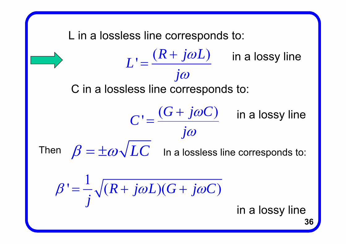
L in a lossless line corresponds to:
( )' G j CCj
( )' R j LLj
in a lossy line
C in a lossless line corresponds to:
in a lossy line
Then LC In a lossless line corresponds to:
1' ( )( )R j L G j Cj
in a lossy line
36

37SPECTROSCOPY GROUPNANOMATERIALS AND CAMBRIDGE UNIVERSITY
DEPARTMENT OF ENGINEERINGELECTRONIC DEVICES
AND MATERIALS GROUP
We get (1.6)j x j x j t
F BV e V e V e e (1.7)j x j x j t
F BI e I e I e e
Substituting β β’ into (1.4) and (1.5) and defining
( )( )R j L G j C j
is the phase constant
And the real term α corresponds to the attenuation along the line and is known as the attenuation constant.
is called propagation constant
37

38SPECTROSCOPY GROUPNANOMATERIALS AND CAMBRIDGE UNIVERSITY
DEPARTMENT OF ENGINEERINGELECTRONIC DEVICES
AND MATERIALS GROUP
VoltageVF
x
For a forward travelling wave:
V = VF e jt e-x = VF e-αx e j(t-βx)
amplitude factor phase factortime variation
38

39SPECTROSCOPY GROUPNANOMATERIALS AND CAMBRIDGE UNIVERSITY
DEPARTMENT OF ENGINEERINGELECTRONIC DEVICES
AND MATERIALS GROUP
0
2( )( )R j L G j C LC j LC
L R :C G At high frequencies, where
The expressions approximate back to those for lossless lines
and
Note:
Thus
LC
39

40SPECTROSCOPY GROUPNANOMATERIALS AND CAMBRIDGE UNIVERSITY
DEPARTMENT OF ENGINEERINGELECTRONIC DEVICES
AND MATERIALS GROUP
I.1.4 Wave velocity: vOur expressions for voltage and current contain 2 exponentials
The one in terms of x: j xe
Gives the spatial dependence of the wave, hence the wavelength:
2
The other: j te
gives the temporal dependence of the wave, hence its frequency:
2f
40

41SPECTROSCOPY GROUPNANOMATERIALS AND CAMBRIDGE UNIVERSITY
DEPARTMENT OF ENGINEERINGELECTRONIC DEVICES
AND MATERIALS GROUP
For a wave velocity v, wavelength and frequency f:
v f
22
v
then
LC since
1vLC
(1.8)
41

42SPECTROSCOPY GROUPNANOMATERIALS AND CAMBRIDGE UNIVERSITY
DEPARTMENT OF ENGINEERINGELECTRONIC DEVICES
AND MATERIALS GROUP
I.1.5 Example: Wavelength An Ethernet Cable has L= 0.22 μHm-1 and C = 86 pFm-1.What is the wavelength at 10 MHz ?
2
LC From
23metres
And
2LC
Then 6 6 12
22 *10*10 0.22*10 *86*10
42

43SPECTROSCOPY GROUPNANOMATERIALS AND CAMBRIDGE UNIVERSITY
DEPARTMENT OF ENGINEERINGELECTRONIC DEVICES
AND MATERIALS GROUP
I.1.6 When must distances be accounted for in AC circuits?
2
4
43

44SPECTROSCOPY GROUPNANOMATERIALS AND CAMBRIDGE UNIVERSITY
DEPARTMENT OF ENGINEERINGELECTRONIC DEVICES
AND MATERIALS GROUP
16L
16L
Wave Relevant
Wave Not Relevant
44

45SPECTROSCOPY GROUPNANOMATERIALS AND CAMBRIDGE UNIVERSITY
DEPARTMENT OF ENGINEERINGELECTRONIC DEVICES
AND MATERIALS GROUP
I.1.7 Example: When is wave theory relevant?A designer is creating a circuit which has a clock rate of 5MHz and has 200mm long tracks for which the inductance (L) and capacitance (C) per unit length are:
L=0.5Hm-1 C=60pFm-1
2
LC From And 2LC
6 6 12
2 36.52 *5*10 0.5*10 *60*10
m
Then
36.5 m is much greater than 200 mm (the size of the circuit board) so that wave theory is irrelevant.
Note: The problem is even less relevant for mains frequencies i.e. 50 Hz. This gives ~3650 km 45