Embed Size (px)
Citation preview
Oxford Semiconductor Ltd. 25 ParkGate, Milton Park, Abingdon, Oxon, OX14 4SH, UK Tel: +44 (0)1235 824900 Fax: +44(0)1235 821141
Oxford Semiconductor 2000OXCB950 Datasheet 1.1 – November 2000
Part No. OXCB950-TQFP-A
FEATURE
• Single 16C950 High performance UART channel • Cardbus/PCI compliant, single-function target
controller. Fully compliant to PC Card Standard 7.0*, and PCI Bus Specification 2.2, Power Management 1.0.
• Function access to pre-configure UART prior to handover to generic device drivers.
• UART fully software compatible with 16C550-type devices.
• Baud rates up to 15Mbps in asynchronous mode and 60Mbps in external 1x clock mode
• 128-byte deep FIFO per transmitter and receiver • Flexible clock prescaler from 1 to 31.875 • Automated in-band flow control using programmable
Xon/Xoff in both directions • Automated out-of-band flow control using CTS#/RTS#
and/or DSR#/DTR#
• Arbitrary trigger levels for receiver and transmitter FIFO interrupts and automatic in-band and out-of-band flow control
• Infra-red (IrDA) receiver and transmitter operation • 9-bit data framing as well as 5,6,7 and 8 • Global Interrupt Status and readable FIFO levels to
facilitate implementation of efficient device drivers • Detection of bad data in the receiver FIFO • Operation via IO or memory mapping. • 2 Multi-purpose I/O pins which can be configured as
interrupt input or ‘wake-up’ pins • Auto-detection of optional MicrowireTM based
EEPROM, to reconfigure device. Autodetected.
• 3.3V operation • 100 pin TQFP package
* Compliance to PC Card Standard 7.1 requires small external circuitry.
DESCRIPTION
The OXCB950 is a single chip UART solution for either cardbus or PCI-based serial add-in cards. It is a single function device, offering memory or IO mapped access to the ultra-high performance OX16C950 UART. This UART is the fastest available PC-compatible UART, offering data rates up to 15Mbps and 128-deep transmitter and receiver FIFOs. The deep FIFOs reduce CPU overhead and allow utilisation of higher data rates. The UART is software compatible with the widely used industry-standard 16C550 devices and compatibles, as well as the OX16C95x family of high performance UARTs. In addition to increased performance and FIFO size, the UART also provides the full set of OX16C95x enhanced features including automated in-band flow control, readable FIFO levels etc. A set of local registers is available to enhance device driver efficiency and reduce interrupt latency. The internal UART
has features such as shadowed FIFO fill levels, an interrupt source register and Good-Data Status, readable in one DWORD register visible to logical function0 in IO space and memory space. The efficient 32-bit, 33MHz target-only interface is compliant with both the cardbus sections of the PC CARD Standard, release 7.0*, and the PCI bus specifications version 2.2 and version 1.0 of PCI Power Management Specification. For full flexibility, all the default register values can be overwritten using an optional MicrowireTM serial EEPROM. This EEPROM can also be used to provide function access to pre-configure the UART into enhanced modes prior to any cardbus/PCI configuration accesses and before control is handed to generic device drivers.
OXCB950 Integrated High Performance UART
Cardbus / PCI interface
Data Sheet Revision 1.1 Page 2
OXCB950
OXFORD SEMICONDUCTOR LTD.
CONTENTS
1 PERFORMANCE COMPARISON..................................................................................................4 1.1 IMPROVEMENTS OF THE OXCB950 OVER DISCRETE SOLUTIONS: ........................................................................... 4 2 BLOCK DIAGRAM.......................................................................................................................5
3 PIN INFORMATION .....................................................................................................................6
4 PIN DESCRIPTIONS ....................................................................................................................7
5 CONFIGURATION & OPERATION .............................................................................................11
6 PCI TARGET CONTROLLER .....................................................................................................12 6.1 OPERATION........................................................................................................................................................................ 12 6.2 CONFIGURATION SPACE ................................................................................................................................................. 13 6.2.1 CARDBUS / PCI CONFIGURATION SPACE REGISTER MAP..................................................................................... 13 6.3 ACCESSING THE UART FUNCTION ................................................................................................................................ 15 6.3.1 CARDBUS/PCI ACCESS TO THE INTERNAL UART.................................................................................................... 15 6.4 ACCESSING LOCAL CONFIGURATION REGISTERS .................................................................................................... 16 6.4.1 LOCAL CONFIGURATION AND CONTROL REGISTER ‘LCC’ (OFFSET 0X00) ......................................................... 16 6.4.2 MULTI-PURPOSE I/O CONFIGURATION REGISTER ‘MIC’ (OFFSET 0X04) ............................................................. 17 6.4.3 UART MIRROR REGISTER ‘UMR’ (OFFSET 0X08): .................................................................................................... 18 6.4.4 GLOBAL INTERRUPT STATUS AND CONTROL REGISTER ‘GIS’ (OFFSET 0X0C) ................................................ 19 6.5 CARDBUS/ PCI INTERRUPT ............................................................................................................................................. 20 6.6 CARDBUS/PCI POWER MANAGEMENT.......................................................................................................................... 21 6.6.1 POWER MANAGEMENT VIA UART/ MIO PINS............................................................................................................ 21 6.6.2 POWER REPORTING..................................................................................................................................................... 22 6.6.3 CARDBUS POWER MANAGEMENT ............................................................................................................................. 23 6.7 CARDBUS STATUS REGISTERS ..................................................................................................................................... 24 6.8 CARDBUS TUPLE INFORMATION ................................................................................................................................... 26
7 INTERNAL OX16C950 UART .....................................................................................................27 7.1 OPERATION – MODE SELECTION ................................................................................................................................... 27 7.1.1 450 MODE ....................................................................................................................................................................... 27 7.1.2 550 MODE ....................................................................................................................................................................... 27 7.1.3 750 MODE ....................................................................................................................................................................... 27 7.1.4 650 MODE ....................................................................................................................................................................... 27 7.1.5 950 MODE ....................................................................................................................................................................... 28 7.2 REGISTER DESCRIPTION TABLES ................................................................................................................................. 29 7.3 RESET CONFIGURATION ................................................................................................................................................. 33 7.3.1 HARDWARE RESET....................................................................................................................................................... 33 7.3.2 SOFTWARE RESET ....................................................................................................................................................... 33 7.4 TRANSMITTER AND RECEIVER FIFOS........................................................................................................................... 34 7.4.1 FIFO CONTROL REGISTER ‘FCR’ ................................................................................................................................ 34 7.5 LINE CONTROL & STATUS............................................................................................................................................... 35 7.5.1 FALSE START BIT DETECTION .................................................................................................................................... 35 7.5.2 LINE CONTROL REGISTER ‘LCR’ ................................................................................................................................ 35 7.5.3 LINE STATUS REGISTER ‘LSR’.................................................................................................................................... 36 7.6 INTERRUPTS & SLEEP MODE ......................................................................................................................................... 37 7.6.1 INTERRUPT ENABLE REGISTER ‘IER’ ........................................................................................................................ 37 7.6.2 INTERRUPT STATUS REGISTER ‘ISR’ ........................................................................................................................ 38 7.6.3 INTERRUPT DESCRIPTION .......................................................................................................................................... 38 7.6.4 SLEEP MODE ................................................................................................................................................................. 39 7.7 MODEM INTERFACE ......................................................................................................................................................... 39 7.7.1 MODEM CONTROL REGISTER ‘MCR’.......................................................................................................................... 39

Data Sheet Revision 1.1 Page 3
OXCB950
OXFORD SEMICONDUCTOR LTD.
7.7.2 MODEM STATUS REGISTER ‘MSR’ ............................................................................................................................. 40 7.8 OTHER STANDARD REGISTERS ..................................................................................................................................... 40 7.8.1 DIVISOR LATCH REGISTERS ‘DLL & DLM’ ................................................................................................................. 40 7.8.2 SCRATCH PAD REGISTER ‘SPR’................................................................................................................................. 40 7.9 AUTOMATIC FLOW CONTROL......................................................................................................................................... 41 7.9.1 ENHANCED FEATURES REGISTER ‘EFR’................................................................................................................... 41 7.9.2 SPECIAL CHARACTER DETECTION ............................................................................................................................ 42 7.9.3 AUTOMATIC IN-BAND FLOW CONTROL ..................................................................................................................... 42 7.9.4 AUTOMATIC OUT-OF-BAND FLOW CONTROL........................................................................................................... 42 7.10 BAUD RATE GENERATION............................................................................................................................................... 43 7.10.1 GENERAL OPERATION ................................................................................................................................................. 43 7.10.2 CLOCK PRESCALER REGISTER ‘CPR’ ....................................................................................................................... 43 7.10.3 TIMES CLOCK REGISTER ‘TCR’................................................................................................................................... 43 7.10.4 EXTERNAL 1X CLOCK MODE....................................................................................................................................... 45 7.10.5 CRYSTAL OSCILLATOR CIRCUIT ................................................................................................................................ 45 7.11 ADDITIONAL FEATURES .................................................................................................................................................. 45 7.11.1 ADDITIONAL STATUS REGISTER ‘ASR’ ...................................................................................................................... 45 7.11.2 FIFO FILL LEVELS ‘TFL & RFL’ ..................................................................................................................................... 46 7.11.3 ADDITIONAL CONTROL REGISTER ‘ACR’ .................................................................................................................. 46 7.11.4 TRANSMITTER TRIGGER LEVEL ‘TTL’ ........................................................................................................................ 47 7.11.5 RECEIVER INTERRUPT. TRIGGER LEVEL ‘RTL’ ........................................................................................................ 47 7.11.6 FLOW CONTROL LEVELS ‘FCL’ & ‘FCH’...................................................................................................................... 47 7.11.7 DEVICE IDENTIFICATION REGISTERS ....................................................................................................................... 47 7.11.8 CLOCK SELECT REGISTER ‘CKS’ ............................................................................................................................... 48 7.11.9 NINE-BIT MODE REGISTER ‘NMR’............................................................................................................................... 48 7.11.10 MODEM DISABLE MASK ‘MDM’ .................................................................................................................................... 49 7.11.11 READABLE FCR ‘RFC’ ................................................................................................................................................... 49 7.11.12 GOOD-DATA STATUS REGISTER ‘GDS’ ..................................................................................................................... 49 7.11.13 DMA STATUS REGISTER ‘DMS’ ................................................................................................................................... 50 7.11.14 PORT INDEX REGISTER ‘PIX’....................................................................................................................................... 50 7.11.15 CLOCK ALTERATION REGISTER ‘CKA’....................................................................................................................... 50 8 SERIAL EEPROM SPECIFICATION ...........................................................................................51 8.1 EEPROM DATA ORGANISATION ..................................................................................................................................... 51 8.1.1 ZONE0: HEADER............................................................................................................................................................ 51 8.1.2 ZONE1 : POWER MANAGEMENT DATA, DATA_SCALE ZONE ................................................................................. 52 8.1.3 ZONE2: LOCAL CONFIGURATION REGISTER ZONE ................................................................................................ 53 8.1.4 ZONE 3 : CARDBUS INFORMATION STRUCTURE..................................................................................................... 53 8.1.5 ZONE4: PCI CONFIGURATION REGISTERS ............................................................................................................... 54 8.1.6 ZONE5: FUNCTION ACCESS ........................................................................................................................................ 55
9 COMPLIANCE TO PC CARD STANDARDS, 7.0 AND 7.1 ............................................................57
10 OPERATING CONDITIONS .....................................................................................................60
11 DC ELECTRICAL CHARACTERISTICS ...................................................................................61 11.1 NORMAL 3.3V I/O BUFFERS............................................................................................................................................. 61 11.2 5.0V TOLERANT I/O BUFFERS........................................................................................................................................ 61 11.3 DUAL MODE (CARDBUS/PCI) I/O BUFFERS ................................................................................................................. 62
12 POWER CONSUMPTION MEASUREMENTS ...........................................................................63 12.1 STATIC CURRENT CONSUMPTION ................................................................................................................................. 63 12.2 CURRENT CONSUMPTION IN APPLICATION ................................................................................................................. 63 13 TIMING WAVEFORMS............................................................................................................64
14 PHYSICAL PACKAGE DETAILS.............................................................................................66

Data Sheet Revision 1.1 Page 4
OXCB950
OXFORD SEMICONDUCTOR LTD.
1 PERFORMANCE COMPARISON
Feature OXCB950 16C550 +
PLX9050 16C650 + PLX9050
Support for PCI Power Management yes no No Zero wait-state read/write operation yes no No No. of external interrupt source pins 2 2 2
DWORD access to UART Interrupt Source Registers & FIFO Levels
yes no No
Good-Data status yes no No Full Plug and Play with external EEPROM yes yes Yes
External 1x baud rate clock yes no No Max baud rate in normal mode 15 Mbps 115 Kbps 1.5 Mbps
Max baud rate in 1x clock mode 60 Mbps n/a n/a FIFO depth 128 16 64 Sleep mode yes no Yes
Auto Xon/Xoff flow yes no Yes Auto CTS#/RTS# flow yes no Yes Auto DSR#/DTR# flow yes no No
No. of Rx interrupt thresholds 128 4 4 No. of Tx interrupt thresholds 128 1 4 No. of flow control thresholds 128 n/a 4 Transmitter empty interrupt yes no No
Readable status of flow control yes no No Readable FIFO levels yes no No Clock prescaler options 248 n/a 2
Rx/Tx disable yes no No Software reset yes no No
Device ID yes no No 9-bit data frames yes no No
RS485 buffer enable yes no No Infra-red (IrDA) yes no Yes
Table 1: OXCB950 performance compared with PLX + generic UART combinations in PCI mode
1.1 Improvements of the OXCB950 over discrete solutions:
Improved access timing: Access to the internal UART requires zero or one PCI wait states. A cardbus/PCI read transaction from the internal UART can complete within five PCI clock cycles and a write transaction to the internal UART can complete within four PCI clock cycles. Reduces interrupt latency: The OXCB950 offers shadowed FIFO levels and Interrupt status registers of the internal UART, as well as general device interrupt status, to reduce the device driver interrupt latency. Power management: The OXCB950 complies with the Cardbus Power Management Specification, given by the PC CARD standard release 7.0/7.1, the PCI Power Management Specification 1.0 and the PC98/99 Power Management specifications, by offering the extended capabilities for Power Management and supporting the power states D0, D2 and D3. This achieves significant power savings by allowing device drivers to power down the cardbus/PCI function and disable the UART channel.
Data Sheet Revision 1.1 Page 5
OXCB950
OXFORD SEMICONDUCTOR LTD.
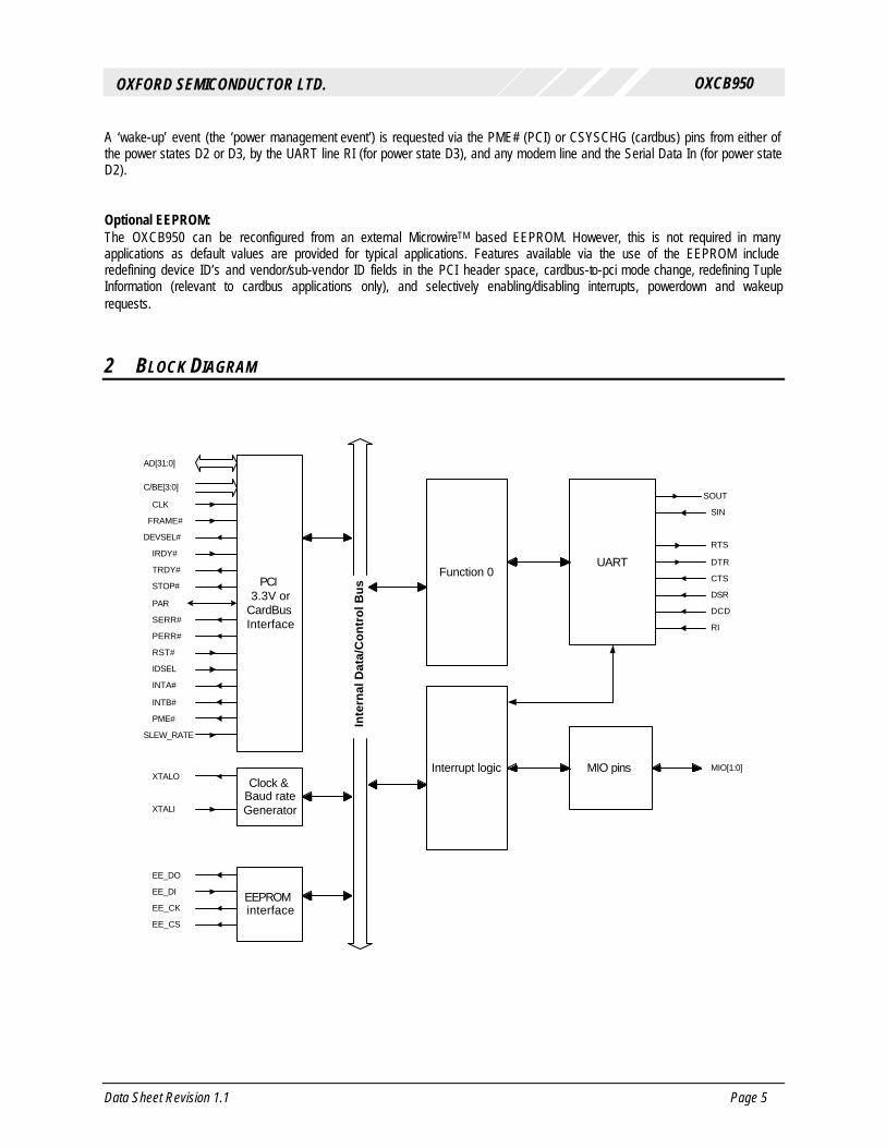
A ‘wake-up’ event (the ‘power management event’) is requested via the PME# (PCI) or CSYSCHG (cardbus) pins from either of the power states D2 or D3, by the UART line RI (for power state D3), and any modem line and the Serial Data In (for power state D2). Optional EEPROM: The OXCB950 can be reconfigured from an external MicrowireTM based EEPROM. However, this is not required in many applications as default values are provided for typical applications. Features available via the use of the EEPROM include redefining device ID’s and vendor/sub-vendor ID fields in the PCI header space, cardbus-to-pci mode change, redefining Tuple Information (relevant to cardbus applications only), and selectively enabling/disabling interrupts, powerdown and wakeup requests.
2 BLOCK DIAGRAM
PCI3.3V or
CardBusInterface
AD[31:0]
C/BE[3:0]
CLK
FRAME#
DEVSEL#
IRDY#
TRDY#
STOP#
PAR
SERR#
PERR#
RST#
IDSEL
INTA#
INTB#
PME#
Clock &Baud rateGenerator
XTALO
XTALI
EEPROMinterface
EE_DO
EE_DI
EE_CK
EE_CS
Inte
rna
l D
ata
/Co
ntr
ol
Bu
s
Function 0
Interrupt logic
UART
MIO pins
SOUT
SIN
RTS
DTR
CTS
DSR
DCD
RI
MIO[1:0]
SLEW_RATE

Data Sheet Revision 1.1 Page 6
OXCB950
OXFORD SEMICONDUCTOR LTD.
3 PIN INFORMATION
100 pin TQFP (14mm x 14mm) AD20 | AD21 | | AD22 | | | Z_SERR | | | | VDD3OP_CB | | | | | VSS0P_CB | | | | | | AD23 | | | | | | | IDSEL | | | | | | | | Z_CBE3 | | | | | | | | | AD24 | | | | | | | | | | VSS0P_CB | | | | | | | | | | | VSSOP_CB | | | | | | | | | | | | VDD3I_CB | | | | | | | | | | | | | VSSI_CB | | | | | | | | | | | | | | AD25 | | | | | | | | | | | | | | | AD26 | | | | | | | | | | | | | | | | CSYSCHG | | | | | | | | | | | | | | | | | AD27 | | | | | | | | | | | | | | | | | | AD28 | | | | | | | | | | | | | | | | | | | VDD3OP_CB | | | | | | | | | | | | | | | | | | | | VSS0P_CB | | | | | | | | | | | | | | | | | | | | | AD29 | | | | | | | | | | | | | | | | | | | | | | AD30 | | | | | | | | | | | | | | | | | | | | | | | AD31 | | | | | | | | | | | | | | | | | | | | | | | | Z_PME | | | | | | | | | | | | | | | | | | | | | | | | | | | | | | | | | | | | | | | | | | | | | | | | | | VSS0P_CB -- -- VSS0 AD19 -- -- EXT_DATA_OUT AD18 -- -- Z_RTS AD17 -- -- Z_DTR Z_CBE2 -- -- Z_CTS VDD3OP_CB -- -- Z_DSR VSS0P_CB -- -- Z_DCD Z_FRAME -- -- Z_RI Z_IRDY -- -- EXT_DATA_IN Z_TRDY -- -- VDD0 Z_RESET -- -- VSS0 VSSI_CB -- -- VDDIP PCI_CLK -- -- VDDIP VDD3I_CB -- -- XTLO VSSOP_CB -- -- XTLI VDD3OP_CB -- -- VSSIP VSS0P_CB -- -- TEST0 Z_DEVSEL -- -- TEST1 Z_CINT -- . -- BUFFER_SLEW_RATE Z_STOP -- . -- EEPROM_DI Z_PERR -- . -- EEPROM_DO VSS0P_CB -- 97 -- EEPROM_CS PAR -- 98 -- EEPROM_SK Z_CBE1 -- 99 -- MIO1 AD16 -- 1 2 3 4 5 6 7... -- MIO0 | | | | | | | | | | | | | | | | | | | | | | | | | | | | | | | | | | | | | | | | | | | | | | | | | | | | | | | | | | | | | | | | | | | | | | | | | | AD0 | | | | | | | | | | | | | | | | | | | | | | | AD1 | | | | | | | | | | | | | | | | | | | | | | AD2 | | | | | | | | | | | | | | | | | | | | | AD3 | | | | | | | | | | | | | | | | | | | | VDD30P_CB | | | | | | | | | | | | | | | | | | | VSS0P_CB | | | | | | | | | | | | | | | | | | AD4 | | | | | | | | | | | | | | | | | AD5 | | | | | | | | | | | | | | | | AD6 | | | | | | | | | | | | | | | AD7 | | | | | | | | | | | | | | Z_CBE0 | | | | | | | | | | | | | VDD3I_CB | | | | | | | | | | | | VSSI_CB | | | | | | | | | | | VSS0P_CB | | | | | | | | | | AD8 | | | | | | | | | AD9 | | | | | | | | AD10 | | | | | | | AD11 | | | | | | VDD30P_CB | | | | | VSS0P_CB | | | | AD12 | | | AD13 | | AD14 | VSSOP_CB AD15

Data Sheet Revision 1.1 Page 7
OXCB950
OXFORD SEMICONDUCTOR LTD.
4 PIN DESCRIPTIONS
Cardbus/PCI bus Pins Dir1 Name Description 52, 53, 54, 57, 58, 60, 61, 66,
69, 73, 74, 75, 77, 78, 79, 100, 1, 3, 4, 5, 8, 9, 10, 11, 16, 17,
18, 19, 22, 23, 24, 25
C/P_I/O AD[31:0] Multiplexed Address/Data bus.
67, 80, 99, 15 C/P_I C/BE[3:0]# Multiplexed Command/Byte enable.
88 CP_I CLK System clock 83 CP_I FRAME# Cycle Frame1.
93 CP_O DEVSEL# Device Select 84 CP_I IRDY# Initiator ready 85 CP_O TRDY# Target ready 95 CP_O STOP# Target Stop request 98 CP_I/O PAR Parity 72 CP_O SERR# System error 96 CP_I/O PERR# Parity error 68 CP_I IDSEL Initialisation device select
For PCI applications this pin must be connected to the IDSEL pin on the PCI connector. For cardbus applications, there is no IDSEL signal, so this pin must be tied to Vdd (3.3v) via a pull-up on the board. (10K recommended).
86 CP_I RST# System reset 94 CP_OD INTA# /CINT# Interrupt Pin. For both cardbus and pci applications 59 CP_O CSYSCHG Power management event signal, for Cardbus applications
This pin must be No-Connect (NC) for PCI applications. 51 CP_OD PME# Power management event signal, for PCI applications
This pin must be No-Connect (NC) for cardbus applications. 32 I SLEW_RATE Slew rate control for cardbus/pci outputs
For cardbus applications, this must be tied to Vdd on the board. For PCI applications, this must be tied to Gnd on the board.
1 For cardbus applications, the pin z_frame requires a pull-up (4k7) on the board. See PC Card Standard 7.0/7.1, section 5.3.3.3.3 “pull-up resistor requirements”.

Data Sheet Revision 1.1 Page 8
OXCB950
OXFORD SEMICONDUCTOR LTD.
UART pins Dir1 Name Description
49 T_O EXT_DATA_OUT IrDA_Out
UART serial data output UART IrDA data output when MCR[6] of the corresponding channel is set in enhanced mode
42 T_I
T_I
EXT_DATA_IN IrDA_In
UART serial data input UART IrDA data input when IrDA mode is enabled (see above)
44 T_I DCD# Active-low modem data-carrier-detect input 47 T_O
T_O
T_O
DTR# 485_En Tx_Clk_Out
Active-low modem data-terminal-ready output. If automated DTR# flow control is enabled, the DTR# pin is asserted and deasserted if the receiver FIFO reaches or falls below the programmed thresholds, respectively. In RS485 half-duplex mode, the DTR# pin may be programmed to reflect the state of the the transmitter empty bit to automatically control the direction of the RS485 transceiver buffer (see register ACR[4:3]) Transmitter 1x clock (baud rate generator output). For isochronous applications, the 1x (or Nx) transmitter clock may be asserted on the DTR# pins (see register CKS[5:4])
48 T_O RTS# Active-low modem request-to-send output. If automated RTS# flow control is enabled, the RTS# pin is deasserted and reasserted whenever the receiver FIFO reaches or falls below the programmed thresholds, respectively.
46 T_I CTS# Active-low modem clear-to-send input. If automated CTS# flow control is enabled, upon deassertion of the CTS# pin, the transmitter will complete the current character and enter the idle mode until the CTS# pin is reasserted. Note: flow control characters are transmitted regardless of the state of the CTS# pin.
45 T_I
T_I
DSR# Rx_Clk_In
Active-low modem data-set-ready input. If automated DSR# flow control is enabled, upon deassertion of the DSR# pin, the transmitter will complete the current character and enter the idle mode until the DSR# pin is reasserted. Note: flow control characters are transmitted regardless of the state of the DSR# pin External receiver clock for isochronous applications. The Rx_Clk_In is selected when CKS[1:0] = ‘01’.
43 T_I
T_I
RI# Tx_Clk_In
Active-low modem Ring-Indicator input External transmitter clock. This clock can be used by the transmitter (and indirectly by the receiver) when CKS[6]=’1’.
37 O XTLO Crystal oscillator output 36 I XTLI Crystal oscillator input (10MHz – 40 MHz) or external clock
pin. Maximum frequency 60MHz

Data Sheet Revision 1.1 Page 9
OXCB950
OXFORD SEMICONDUCTOR LTD.
Multi-purpose & External interrupt pins
Dir1 Name Description
26 27
T_I/O T_I/O
MIO[0] MIO[1]
Multi-purpose I/O pins. Can be driven high or low, or be used to invoke cardbus/PCI interrupts, and powerdown, wakeup requests.
EEPROM pins 28 O EE_CK EEPROM clock 29 O EE_CS EEPROM active-high Chip Select 31 IU EE_DI EEPROM data in (to be connected to the EEPROM DO
pin). When the optional serial EEPROM is connected, this pin should be pulled up using an external 1-10k resistor. When the EEPROM is not used, this external pull-up is not required (internal pull-up is sufficient).
30 O EE_DO EEPROM data out. (to be connected to the EEPROM DI pin)
Miscellaneous pins 34 ID TEST0 Test Pin 0. Should be held low at all times. 33 ID TEST1 Test Pin 1. Should be held low at all times
Power and ground2 89, 14, 63 V VDD3I_CB Supplies power to the pre-drive area of the dual mode
cardbus/pci IO buffers. 56, 71, 81, 91, 7, 21 V VDD3OP_CB Supplies power to the output drive of the dual mode
cardbus/pci IO buffers. 38, 39 V VDDIP Supplies power to the core-logic and pre-drive area of the
standard IO buffers. 41, V VDDO Suppiles power to the output drive of standard IO buffers.
62, 87, 13 G VSSI_CB Supplies ground to the pre-drive area of the dual mode cardbus/pci IO buffers.
55, 64,65,70, 76, 82, 90, 92, 97, 2, 6, 12, 20,
G VSSOP_CB Supplies ground to the output drive of the dual mode cardbus/pci IO buffers.
35 G VSSIP Supplies gnd to the core-logic and pre-drive area of the standard IO buffers.
40, 50 G VSSO Supplies gnd to the output drive of standard IO buffers.
Table: Pin Descriptions Note 1: Direction key: I 3.3v Input, TTL compatible ID 3.3v Input with pull-down, TTL compatible IU 3.3v Input with pull-up, TTL compatible O 3.3v Output, TTL compatible T_O 5.0v tolerant TTL output T_I 5.0v tolerant TTL input T_I/O 5.0v tolerant TTL Bi-directional
C/P_I Cardbus/PCI compatible input C/P_O Cardbus/PCI compatible output C/P_I/O Cardbus/PCI compatible bi-directional C/P_OD Cardbus/PCI compatible open drain G Ground V 3.3V power
Note 2: Power & Ground There are several types of VDD and VSS in this design, providing not only power for the internal (core) and I/O pad area but also special power lines to the dual mode cardbus/pci I/O buffers. These power rails are not connected internally. This precaution reduces the effects of simultaneous switching outputs and undesirable RF radiation from the chip. Further precaution is taken by segmenting the GND and VDD rails to isolate the PCI and UART pins.
Data Sheet Revision 1.1 Page 10
OXCB950
OXFORD SEMICONDUCTOR LTD.
Pinout Assignment This device implements the “common” silicon requirements given in the PC Card Standard, release 7.x. The pinouts for this device have been assigned specifically to align the cardbus signals to the cardbus connector without any signal crossovers. Since the assignment of signal pins on the cardbus connector is in a different sequence than those on the PCI connector (due to the limitations of the cardbus connector) then for the PCI environment signal crossovers do inevtiably occur. The following signal lines are affected for the PCI environment : SERR#, AD16, INTA, CLK, and RST#.

Data Sheet Revision 1.1 Page 11
OXCB950
OXFORD SEMICONDUCTOR LTD.
5 CONFIGURATION & OPERATION
The OXCB950 is configured by system start-up software during the bootstrap process that follows bus reset. By default, the device powers-up in the cardbus mode and for this application mode, the system examines the Cardbus CIS pointer value contained in the predefined PCI Header region (at Dword 0Ahex) to locate the start of the Cardbus Information Structure (CIS). It then traverses the tuple information contained in this CIS areaNOTE1 to identify the device type and the necessary resources requested by the device. For the PCI application mode, whereby the device’s default cardbus mode is overridden into the PCI mode though the use of the optional EEPROM (this takes place prior to any configuration accesses), the system scans the PCI bus and reads the vendor and device identification codes from any devices it finds and the resources being requested. For both cardbus and PCI applications, the system then loads the device-driver software according to this information and configures the I/O, memory and interrupt resources. Device drivers can then access the functions at
the assigned addresses in the usual fashion, with the improved data throughput provided by cardbus/PCI buses. A set of local configuration registers have been provided that can be used to control the device’s characteristics (such as interrupt handling) and report internal functional status. This is on top of the UART registers and the registers contained in both the PCI configuration Space and the Cardbus Information Structure (CIS). These local registers can be set up by device drivers or from the optional EEPROM. The EEPROM can also be used to redefine the reset values of most register areas to tailor the device to the end users requirements if the default values do not meet the specific requirements of the manufacturer, such as the identification registers. As an additional enhancement, the EEPROM can be used to pre-program the UART, allowing pre-configuration, without requiring device driver changes. This allows the enhanced features of the integrated UART to be in place prior to handover to any generic device drivers.
NOTE1 Windows Support for Cardbus applications, treats the information contained in the CIS area as “supplemental” information for devices that are not fully described using the PCI configuration Space. This means that it is possible that provided the PCI header space implements the minimum fields as recommended by Microsoft (the cardbus “Allocated” and “Reserved” fields are defined) then Windows will not utilise the information contained in the CIS.

Data Sheet Revision 1.1 Page 12
OXCB950
OXFORD SEMICONDUCTOR LTD.
6 PCI TARGET CONTROLLER
6.1 Operation
The OXCB950 responds to the following cardbus/PCI transactions:- • Configuration access: For cardbus applications, the
OXCB950 responds to type 0 configuration reads and writes if the bus address is selecting the configuration registers for function 0. For pci applications, the OXCB950 will respond to the same configuration cycles provided that the signal IDSEL is also asserted The device will respond to these configuration transactions by asserting DEVSEL#. Data transfer then follows. Any other configuration transaction will be ignored by the OXCB950.
• IO reads/writes: The address is compared with the
addresses reserved in the I/O Base Address Registers (BARs). If the address falls within one of the assigned ranges, the device will respond to the IO transaction by asserting DEVSEL#. Data transfer follows this address phase. For all modes, only byte accesses are possible to the function BARs (excluding the local configuration registers for which WORD, DWORD access is supported). For IO accesses to these regions, the controller compares AD[1:0] with the byte-enable signals as defined in the PCI specification. The access is always completed; however if the correct BE signal is not present the transaction will have no effect.
• Memory reads/writes: These are treated in the same
way as I/O transactions, except that the memory ranges are used. With the exception of Memory accesses to the local configuration registers and the cardbus status registers, Memory access to single-byte regions such as the UART registers is always expanded to DWORDs in the OXCB950. In other words, the OXCB950 reserves a DWORD per byte in single-byte regions. The device allows the user to define the active byte lane using LCC[4:3] so that in Big-Endian systems the hardware can swap the byte lane automatically. For Memory mapped access in single-byte regions, the OXCB950 compares the asserted byte-enable with the selected byte-lane in LCC[4:3] and completes the operation if a match occurs, otherwise the access will complete normally on the PCI bus, but it will have no effect on the UART.
• All other cycles (64-bit, special cycles, reserved
encoding etc.) are ignored.
The OXCB950 will complete all transactions as disconnect-with-data, i.e. the device will assert the STOP# signal alongside TRDY#, to ensure that the Bus Master does not continue with a burst access. The exception to this is Retry, which will be signalled in response to any access while the OXCB950 is reading from the serial EEPROM. The OXCB950 performs medium-speed address decoding as defined by the PCI specification. It asserts the DEVSEL# bus signal two clocks after FRAME# is first sampled low on all bus transaction frames which address the chip. Fast back-to-back transactions are supported by the OXCB950 as a target, so a bus master can perform faster sequences of write transactions to the UART registers, the PCI configuration space and the local configuration registers when an inter-frame turn-around cycle is not required. The device supports any combination of byte-enables for accesses to the PCI Configuration Registers, the Local Configuration registers, the Cardbus Information Structure, and the cardbus status registers. If a byte-enable is not asserted, that byte is unaffected by a write operation and undefined data is returned upon a read. The OXCB950 performs parity generation and checking on all cardbus/PCI bus transactions as defined by the 2 standards. If a parity error occurs during the bus address phase, the device will report the error in the standard way by asserting the SERR# bus signal. However if that address/command combination is decoded as a valid access, it will still complete the transaction as though the parity check was correct. The OXCB950 does not support any kind of caching or data buffering, other than those in the UART function. In general, all registers cannot be pre-fetched because there may be side-effects on reads.

Data Sheet Revision 1.1 Page 13
OXCB950
OXFORD SEMICONDUCTOR LTD.
6.2 Configuration space
The OXCB950 is a single function device, with one PCI configuration space (and for the default cardbus mode, one cardbus information structure). All the required fields in the predefined PCI header region have been implemented. This includes those fields in the cardbus PC Card Standard that are termed “allocated” and “reserved” for cardbus applications. This implementation is a specific requirement for cardbus support in Windows 9x.
The device dependant region of the PCI configuration space contains the cardbus/pci Power Management Extended Capability register set and (for the cardbus mode only) the Tuples making up the Cardbus Information Structure. The format of the PCI configuration space, for cardbus and pci modes, is as shown in the Table below. In general, writes to any registers that are not implemented are ignored, and all reads from unimplemented registers return 0.
6.2.1 Cardbus / PCI Configuration Space Register map
Configuration Register Description Offset 31 16 15 0 Address
Device ID Vendor ID 00h Status Command 04h
Class Code Revision ID 08h BIST1 Header Type Reserved Reserved 0Ch
Base Address Register 0 (BAR0) – UART Function in I/O space 10h Base Address Register 1 (BAR 1) - UART Function in Memory space 14h
Base Address Register 2 (BAR 2) – Local Configuration Registers in IO space 18h Base Address Register 3 (BAR3) – Local Configuration Registers in Memory space 1Ch
Base Address Register 4 (BAR4) – Cardbus Status Registers in Memory Space Function Event : Offset +0
Function Event Mask : Offset +4 Function Present State : Offset +8 Function Force Event : Offset +12
20h
Reserved (Bar 5) 24h Cardbus CIS Pointer 28h
Subsystem ID Subsystem Vendor ID 2Ch Reserved 30h
Reserved Cap_Ptr 34h Reserved 38h
Reserved Reserved Interrupt Pin Interrupt Line 3Ch
Predefined PCI Header Region Device Dependant PCI Region
Power Management Capabilities (PMC) Next Ptr Cap_ID 40h
Reserved Reserved PMC Control/Status Register (PMCSR) 44h Tuple Byte3* Tuple Byte 2* Tuple Byte1* Tuple Byte 0* 48h
… Tuple Byte (n+1)* Tuple Byte n* 4Ch
* Tuples are available for the Cardbus mode only. These fields return all 0’s for the PCI mode of the device.
Table 2: Cardbus/PCI Configuration space

Data Sheet Revision 1.1 Page 14
OXCB950
OXFORD SEMICONDUCTOR LTD.
Reset value Program read/write Register name Cardbus Mode PCI Mode EEPROM PCI
Vendor ID 0x1415 1 W R Device ID 0x950B 1 W R Command 0x0000 - R/W
Status 0x0290 W(bit 4) R/W Revision ID 0x00 1 - R Class code 0x070006 1 W R
Header type 0x00 - R BAR 0 0x00000001 - R/W BAR 1 0x00000000 - R/W BAR 2 0x00000001 - R/W BAR 3 0x00000000 - R/W BAR 4 0x00000000 - R/W
Cardbus CIS Pointer 0x00000048 (relocate3 = 0) or
0x00000080 (relocate3 = 1)
0x00000000 (no CIS)
W R
Subsystem VID 0x1415 2 W R Subsystem ID 0x0001 2 W R
Cap ptr. 0x40 - R Interrupt line 0x00 1 - R/W Interrupt pin 0x01 W R
Cap ID 0x01 - R Next ptr. 0x00 - R
PM capabilities 0x6C01 W R PMC control/ status
register 0x0000 - R/W
Table 3: Cardbus/PCI configuration space default values 1 For cardbus applications, the PC Card Standard 7.x defines these fields as “Allocated”. However, for cardbus support in Windows, these fields need to be defined to fully support the PCI configuration Space. 2 For cardbus applications, the PC Card Standard 7.x defines these fields as “Reserved”. However, for cardbus support in Windows, these fields need to be defined to fully support the PCI configuration Space. 3 Relocate is a bit in the local configuration registers that can locate the start of the cardbus information structure at DWORD18 or DWORD 32 in the PCI configuration region. This bit is writable only via the optional EEPROM. The default state is 0, so the CIS is available at DWORD18 in the PCI configuration region.
Data Sheet Revision 1.1 Page 15
OXCB950
OXFORD SEMICONDUCTOR LTD.
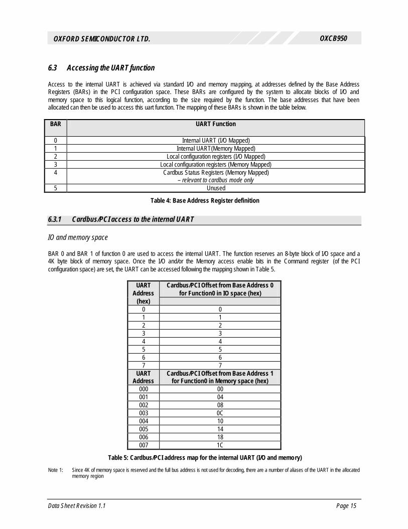
6.3 Accessing the UART function
Access to the internal UART is achieved via standard I/O and memory mapping, at addresses defined by the Base Address Registers (BARs) in the PCI configuration space. These BARs are configured by the system to allocate blocks of I/O and memory space to this logical function, according to the size required by the function. The base addresses that have been allocated can then be used to access this uart function. The mapping of these BARs is shown in the table below. BAR UART Function
0 Internal UART (I/O Mapped) 1 Internal UART(Memory Mapped) 2 Local configuration registers (I/O Mapped) 3 Local configuration registers (Memory Mapped) 4 Cardbus Status Registers (Memory Mapped)
– relevant to cardbus mode only 5 Unused
Table 4: Base Address Register definition
6.3.1 Cardbus/PCI access to the internal UART IO and memory space BAR 0 and BAR 1 of function 0 are used to access the internal UART. The function reserves an 8-byte block of I/O space and a 4K byte block of memory space. Once the I/O and/or the Memory access enable bits in the Command register (of the PCI configuration space) are set, the UART can be accessed following the mapping shown in Table 5.
UART Address
Cardbus/PCI Offset from Base Address 0 for Function0 in IO space (hex)
(hex) 0 0 1 1 2 2 3 3 4 4 5 5 6 6 7 7
UART Address
Cardbus/PCI Offset from Base Address 1 for Function0 in Memory space (hex)
000 00 001 04 002 08 003 0C 004 10 005 14 006 18 007 1C
Table 5: Cardbus/PCI address map for the internal UART (I/O and memory) Note 1: Since 4K of memory space is reserved and the full bus address is not used for decoding, there are a number of aliases of the UART in the allocated
memory region
Data Sheet Revision 1.1 Page 16
OXCB950
OXFORD SEMICONDUCTOR LTD.
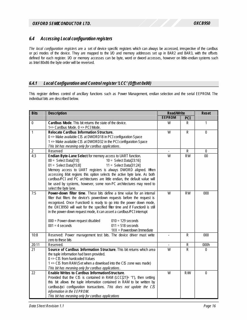
6.4 Accessing Local configuration registers
The local configuration registers are a set of device specific registers which can always be accessed, irrespective of the cardbus or pci modes of the device. They are mapped to the I/O and memory addresses set up in BAR2 and BAR3, with the offsets defined for each register. I/O or memory accesses can be byte, word or dword accesses, however on little-endian systems such as Intel 80x86 the byte order will be reversed.
6.4.1 Local Configuration and Control register ‘LCC’ (Offset 0x00) This register defines control of ancillary functions such as Power Management, endian selection and the serial EEPROM. The individual bits are described below.
Bits Description Read/Write Reset EEPROM PCI 0 Cardbus Mode. This bit returns the state of the device.
1=> Cardbus Mode. 0 => PCI Mode. W R 1
1 Relocate Cardbus Information Structure. 0 => Make available CIS at DWORD18 in PCI configuration Space 1 => Make available CIS at DWORD32 in the PCI configuration Space This bit has meaning only for cardbus applications.
W R 0
2 Reserved - R 0 4:3 Endian Byte-Lane Select for memory access to UART function.
00 = Select Data[7:0] 10 = Select Data[23:16] 01 = Select Data[15:8] 11 = Select Data[31:24] Memory access to UART registers is always DWORD aligned. When accessing 8-bit regions this option selects the active byte lane. As both cardbus/PCI and PC architectures are little endian, the default value will be used by systems, however, some non-PC architectures may need to select the byte lane.
W RW 00
7:5 Power-down filter time . These bits define a time value for an internal filter that filters the device’s powerdown requests before the request is recognised. Once Function0 is ready to go into the power down mode, the OXCB950 will wait for the specified filter time and if Function0 is still in the power-down request mode, it can assert a cardbus/PCI interrupt
W RW 000
000 = Power-down request disabled 001 = 4 seconds
010 = 129 seconds 011 = 518 seconds 1XX = Powerdown Immediate
10:8 Reserved: Power management test bits. The device driver must write zero to these bits
- R 000
20:11 Reserved. - R 000h 21 Source of Cardbus Information Structure. This bit returns which area
the tuple information had been provided. 0 => CIS from hardcoded Values 1 => CIS from RAM (Set when a download into the CIS zone was made) This bit has meaning only for cardbus applications.
W R 0
22 Enable Writes to Cardbus InformationStructure. Provided that the CIS is contained in RAM (LCC[21]= ‘1’), then setting this bit allows the tuple information contained in RAM to be written by cardbus/pci configuration transactions. This does not update the CIS information in the EEPROM. This bit has meaning only for cardbus applications
W R/W 0

Data Sheet Revision 1.1 Page 17
OXCB950
OXFORD SEMICONDUCTOR LTD.
Bits Description Read/Write Reset EEPROM PCI 23 Enable Cardbus Status Registers
When set (1), all interrupt sources and power management events are controlled by the INTR, GWAKE/WKUP fields of the cardbus status registers. This bit has meaning only for cardbus applications
W R/W 0
24 EEPROM Clock. For reads or writes to the external EEPROM , toggle this bit to generate an EEPROM clock (EE_CK pin).
- RW 0
25 EEPROM Chip Select. When 1 the EEPROM chip-select pin EE_CS is activated (high). When 0 EE_CS is de-active (low).
- RW 0
26 EEPROM Data Out. For writes to the EEPROM, this output bit feeds the input-data of the external EEPROM. This bit is output on the devices EE_DO and clocked into the EEPROM by EE_CK.
- RW 0
27 EEPROM Data In. For reads from the EEPROM, this input bit is the output-data (D0) of the external EEPROM connected to EE_DI pin.
- R 1
28 EEPROM Valid. A 1 indicates that a valid EEPROM program header is present
- R X
29 Reload configuration from EEPROM. Writing a 1 to this bit re-loads the configuration from EEPROM. This bit is self-clearing after an EEPROM read
- RW 0
30 Reserved - R 0 31 Reserved - R 0
6.4.2 Multi-purpose I/O Configuration register ‘MIC’ (Offset 0x04) This register configures the operation of the multi-purpose I/O pins ‘MIO[1:0]’ as follows.
Bits Description Read/Write Reset EEPROM PCI 1:0 MIO0 Configuration Register
00 -> MIO0 is a non-inverting input pin 01 -> MIO0 is an inverting input pin 10 -> MIO0 is an output pin driving ‘0’ 11 -> MIO0 is an output pin driving ‘1’
W RW 00
3:2 MIO1 Configuration Register 00 -> MIO1 is a non-inverting input pin 01 -> MIO1 is an inverting input pin 10 -> MIO1 is an output pin driving ‘0’ 11 -> MIO1 is an output pin driving ‘1’
W RW 00
4 MIO0 Power Management Event Enable. A value of ‘1’ enables the MIO0 pin to set the PME_Status bit in the PCI PMCSR register, and hence assert the PME# (pci) or CSYSCHG (cardbus) pin if this option has been enabled. A value of ‘0’ prevents MIO0 from setting the PCI PME_Status bit.
W RW 0
5 MIO1 Power Management Event Enable. A value of ‘1’ enables the MIO1 pin to set the PME_Status bit in the PCI PMCSR register, and hence assert the PME# (pci) or CSYSCHG (cardbus) pin if this option has been enabled. A value of ‘0’ prevents MIO1 from setting the PCI PME_Status bit.
W RW 0
Data Sheet Revision 1.1 Page 18
OXCB950
OXFORD SEMICONDUCTOR LTD.
Bits Description Read/Write Reset EEPROM PCI 6 MIO0 Power Down Filter Control:
A ‘1’ enables the MIO0 pin to invoke a powerdown request via the power down filter (if the filter is enabled). State of MIO0 that causes the powerdown request is governed by the controls MIC[1:0).
W RW 0
7 MIO1 Power Down Filter Control: A ‘1’ enables the MIO1 pin to invoke a powerdown request via the power down filter (if the filter is enabled). State of MIO1 that causes the powerdown request is governed by the controls MIC[3:2).
W RW 0
31:8 Reserved - R 00
6.4.3 UART Mirror Register ‘UMR’ (Offset 0x08): The internal UART’s FIFO levels (both on the transmitter and receiver) and general interrupt source register, is mirrored (shadowed) in the local configuration registers as follows
Bits Description Read/Write Reset EEPROM PCI 7:0 UART Receiver FIFO Level (RFL[7:0]) - R 00h 15:8 UART Transmitter FIFO Level (TFL[7:0]) - R 00h 21:16 UART Interrupt Source Register (ISR[5:0]) - R 01h 26:22 Reserved - R 00h 27 UART Good-Data Status - R 1h 31:28 Reserved - R 0h
Good-Data status for the internal UART is set when all of the following conditions are met: • ISR reads a level0 (no-interrupt pending), a level 2a (receiver data available, a level 2b (receiver time-out) or a level 3
(transmitter THR empty) interrupt • LSR[7] is clear so there is no parity error, framing error or break in the FIFO • LSR[1] is clear so no over-run error has occurred If the device driver software reads the receiver FIFO levels from this register, then if Good-Data status is set, the driver can remove the number of bytes indicated by the FIFO level without the need to read the line status register. This feature enhances the driver efficiency. If the Good-Data status bit is not set, then the software driver should examine the ISR bits. If the ISR indicates a level 4 or higher interrupt, the interrupt is due to a change in the state of modem lines or detection of flow control characters. The device driver-software should then take appropriate measures as would in any other 550/950 driver. When ISR indicates a level 1 (receiver status) interrupt then the driver can examine the Line Status Register (LSR) of the relevant channel. Since reading the LSR clears LSR[7], the device driver-software should either flush or empty the contents of the receiver FIFO, otherwise the Good-Data status will no longer be valid.
Data Sheet Revision 1.1 Page 19
OXCB950
OXFORD SEMICONDUCTOR LTD.
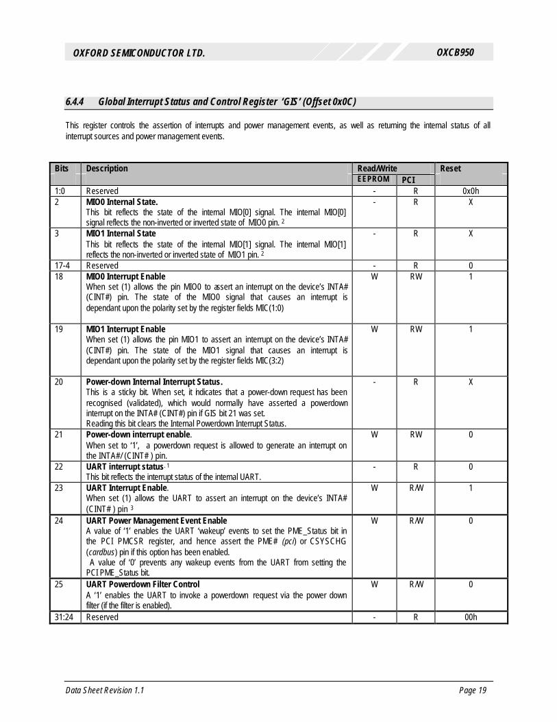
6.4.4 Global Interrupt Status and Control Register ‘GIS’ (Offset 0x0C) This register controls the assertion of interrupts and power management events, as well as returning the internal status of all interrupt sources and power management events.
Bits Description Read/Write Reset EEPROM PCI 1:0 Reserved - R 0x0h 2 MIO0 Internal State.
This bit reflects the state of the internal MIO[0] signal. The internal MIO[0] signal reflects the non-inverted or inverted state of MIO0 pin. 2
-
R
X
3 MIO1 Internal State This bit reflects the state of the internal MIO[1] signal. The internal MIO[1] reflects the non-inverted or inverted state of MIO1 pin. 2
-
R
X
17-4 Reserved - R 0 18 MIO0 Interrupt Enable
When set (1) allows the pin MIO0 to assert an interrupt on the device’s INTA# (CINT#) pin. The state of the MIO0 signal that causes an interrupt is dependant upon the polarity set by the register fields MIC(1:0)
W RW 1
19 MIO1 Interrupt Enable When set (1) allows the pin MIO1 to assert an interrupt on the device’s INTA# (CINT#) pin. The state of the MIO1 signal that causes an interrupt is dependant upon the polarity set by the register fields MIC(3:2)
W RW 1
20 Power-down Internal Interrupt Status. This is a sticky bit. When set, it indicates that a power-down request has been recognised (validated), which would normally have asserted a powerdown interrupt on the INTA# (CINT#) pin if GIS bit 21 was set. Reading this bit clears the Internal Powerdown Interrupt Status.
- R X
21 Power-down interrupt enable. When set to ‘1’, a powerdown request is allowed to generate an interrupt on the INTA#/ (CINT# ) pin.
W RW 0
22 UART interrupt status. 1
This bit reflects the interrupt status of the internal UART. - R 0
23 UART Interrupt Enable. When set (1) allows the UART to assert an interrupt on the device’s INTA# (CINT# ) pin 3
W R/W 1
24 UART Power Management Event Enable A value of ‘1’ enables the UART ‘wakeup’ events to set the PME_Status bit in the PCI PMCSR register, and hence assert the PME# (pci) or CSYSCHG (cardbus) pin if this option has been enabled. A value of ‘0’ prevents any wakeup events from the UART from setting the PCI PME_Status bit.
W R/W 0
25 UART Powerdown Filter Control A ‘1’ enables the UART to invoke a powerdown request via the power down filter (if the filter is enabled).
W R/W 0
31:24 Reserved - R 00h
Data Sheet Revision 1.1 Page 20
OXCB950
OXFORD SEMICONDUCTOR LTD.
Note1 GIS(22) is the inverse of UMR(16). Note 2: The returned value is either the direct state of the corresponding MIO pin or its inverse as configured by the Multi -purpose I/O Configuration register
‘MIC’ (offset 0x04). As the internal MIO can assert a cardbus/PCI interrupt, the inversion feature can define each external interrupt to be defined as active-low or active-high, as controlled by the MIC register.
Note 3: The UART Interrupt Enable register bit is set after a hardware reset to enable the interrupt from the internal UART. This will cater for generic device-
driver software that does not access the Local Configuration Registers. The default setting for the UART Interrupt Enable bit can be changed using the serial EEPROM. Note that even though by default the UART interrupt is enabled in this register, since after a reset the IER register of the UART is disabled then a cardbus/PCI interrupt will not be asserted by the UART after a hardware reset.
6.5 Cardbus/ PCI Interrupt
Interrupts in cardbus/PCI systems are level-sensitive and can be shared. In the OXCB950, there are three sources of interrupts - two from the Multi-Purpose I/O pins (MIO0, MIO1), and one from the internal UART. Since the OXCB950 has only one interrupt pin (INTA# / CINT#), the default routing information contained in the device (the interrupt pin value) results in all interrupts being made available on this single interrupt pin. This default routing may be modified (to disable all interrupts, for example) by writing to the Interrupt Pin field in the cardbus/PCI configuration registers using the serial EEPROM facility. The Interrupt Pin field is normally considered a hard-wired read-only value in cardbus/PCI. It indicates to system software which interrupt pin (if any) is used by a function. The interrupt pin may only be modified using the serial EEPROM facility, and card developers must not set any value which violates the cardbus/PCI specification on this issue. If in doubt, the default routings should be used. Table 6 relates the Interrupt Pin field to the device pin used.
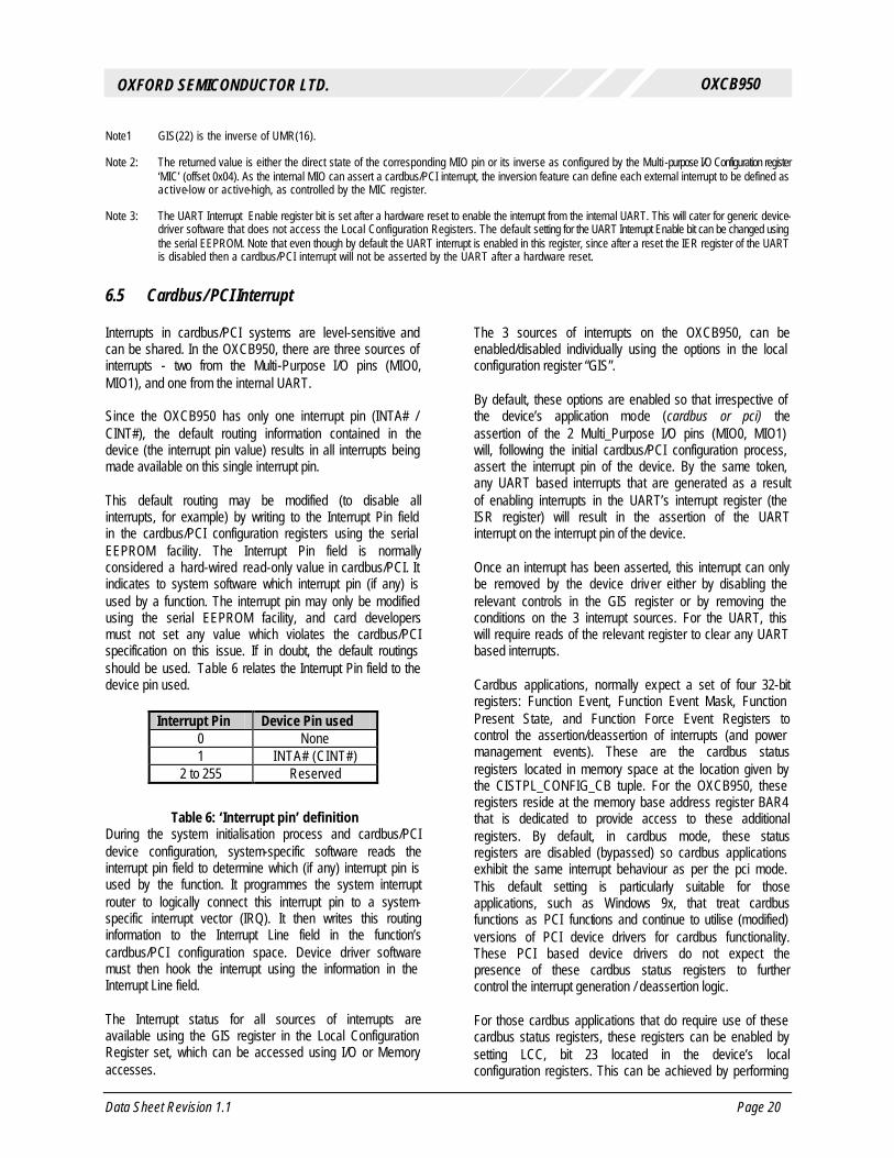
Interrupt Pin Device Pin used 0 None 1 INTA# (CINT#)
2 to 255 Reserved
Table 6: ‘Interrupt pin’ definition During the system initialisation process and cardbus/PCI device configuration, system-specific software reads the interrupt pin field to determine which (if any) interrupt pin is used by the function. It programmes the system interrupt router to logically connect this interrupt pin to a system-specific interrupt vector (IRQ). It then writes this routing information to the Interrupt Line field in the function’s cardbus/PCI configuration space. Device driver software must then hook the interrupt using the information in the Interrupt Line field. The Interrupt status for all sources of interrupts are available using the GIS register in the Local Configuration Register set, which can be accessed using I/O or Memory accesses.
The 3 sources of interrupts on the OXCB950, can be enabled/disabled individually using the options in the local configuration register “GIS”. By default, these options are enabled so that irrespective of the device’s application mode (cardbus or pci) the assertion of the 2 Multi_Purpose I/O pins (MIO0, MIO1) will, following the initial cardbus/PCI configuration process, assert the interrupt pin of the device. By the same token, any UART based interrupts that are generated as a result of enabling interrupts in the UART’s interrupt register (the ISR register) will result in the assertion of the UART interrupt on the interrupt pin of the device. Once an interrupt has been asserted, this interrupt can only be removed by the device driver either by disabling the relevant controls in the GIS register or by removing the conditions on the 3 interrupt sources. For the UART, this will require reads of the relevant register to clear any UART based interrupts. Cardbus applications, normally expect a set of four 32-bit registers: Function Event, Function Event Mask, Function Present State, and Function Force Event Registers to control the assertion/deassertion of interrupts (and power management events). These are the cardbus status registers located in memory space at the location given by the CISTPL_CONFIG_CB tuple. For the OXCB950, these registers reside at the memory base address register BAR4 that is dedicated to provide access to these additional registers. By default, in cardbus mode, these status registers are disabled (bypassed) so cardbus applications exhibit the same interrupt behaviour as per the pci mode. This default setting is particularly suitable for those applications, such as Windows 9x, that treat cardbus functions as PCI functions and continue to utilise (modified) versions of PCI device drivers for cardbus functionality. These PCI based device drivers do not expect the presence of these cardbus status registers to further control the interrupt generation / deassertion logic. For those cardbus applications that do require use of these cardbus status registers, these registers can be enabled by setting LCC, bit 23 located in the device’s local configuration registers. This can be achieved by performing

Data Sheet Revision 1.1 Page 21
OXCB950
OXFORD SEMICONDUCTOR LTD.
an I/O or Memory write to this bit in the local configuration register or by using the optional EEPROM to download into this area. Once these cardbus status registers are enabled, interrupts will only be asserted on the device’s interrupt pin provided that the INTR field is enabled in the Function Event Mask Register (disabled by default) and the corresponding INTR field in the Function Event Register has detected (latched) a valid internal interrupt request. Once asserted, the interrupt on the device’s interrupt pin can only be disabled by either disabling the INTR field in the Function Event Mask register or by writing a “1” to the INTR field of the
Function Event Register. The INTR field in the Function Present State register will reflect the current (non-latched) state of any internal interrupt requests and the INTR field in the Function Force register is available to generate software based interrupts for debug purposes. NOTE : Enabling of the cardbus status registers provides additional controls to the interrupt generation/deassertion logic. The interrupt controls in the local configuration registers must nevertheless be enabled to detect the interrupts from the device’s 3 interrupt sources in the first place.
6.6 Cardbus/PCI Power Management
The OXCB950 is compliant with the Power Management Requirements for cardbus PC cards as detailed in the Electrical Specification of the PC Card Standard, release 7.x. It is also compliant to the PCI Power Management Specification Revision 1.0. The device (function0) implements a set of Power Management registers and supports the power states D0, D2 and D3. Power management is accomplished by handling the power-down and power-up (“power management event”) requests, that are asserted on the device’s interrupt pin and the pins PME#/CSYSCHG respectively. Note, PME# is the power management event for PCI applications and CSYSCHG is the power management event for cardbus applications. The logic behind these signals is identical. Power-down requests are not defined by any of the Power Management specifications. It is a device-specific feature and requires a bespoke device driver implementation. The device driver can either implement the power-down itself or use a special interrupt and power-down features offered by the device to determine when the device is ready for power-down. For PCI applications, it worth noting that the PME# pin can, in certain cases, activate the PME# signal when power is removed from the device, which will cause the PC to wake up from Low-power state D3(cold). To ensure full cross-compatibility with system board implementations, use of an isolator FET is recommended. If Power Management capabilities are not required, the PME# pin can be treated as no-connect. There are no such problems for cardbus applications. The CSYSCHG line is not capable of being asserted on removal of device power.
6.6.1 Power Management via UART/ MIO pins Provided that the necessary controls have been set in the device’s local configuration registers (LCC, MIC, and GIS), the internal UART and the 2 multi_purpose (MIO) pins can be programmed to issue powerdown requests and/or ‘wakeup’ requests (power management events). For the case of the internal UART, the device can be configured to monitor the activity of the serial channel, and issue a power-down interrupt when the UART is inactive (no interrupts pending and both transmitter and receiver are idle). For the case of the MIO pins, the MIO state that governs powerdown is the inverse of the MIO state that asserts the device’s interrupt pin (the INTA# / CINT# line, if that option were to be enabled). This means that when any external device is not interrupting it will automatically begin the powerdown cycle. When either a powerdown request from the internal UART or a powerdown request from the MIO pins has been detected, the internal power management circuitry waits for a period of time as programmed into the Power-Down Filter Time (defined by the local configuration register LCC[7:5]) and if the powerdown requests are still valid i.e. for the UART, this means that the channel is still inactive, then the OXCB950 can issue a powerdown interrupt on the device’s interrupt pin if this option is enabled. Alternatively, the device driver can poll the powerdown status field in the local configuration register GIS[20] to determine a powerdown request. This powerdown filter stops the UART and the MIO pins from issuing too many powerdown interrupts whenever the UART and MIO pin activity is intermittent.

Data Sheet Revision 1.1 Page 22
OXCB950
OXFORD SEMICONDUCTOR LTD.
Upon a power down interrupt, the device driver can change the power-state of the device as required. Note that the power-state of the device is only changed by the device driver and at no point will the OXCB950 change its own power state. The powerdown interrupt merely informs the device driver that this logical function is ready for power down. Before placing the device into the lower power states, the driver must provide the means for the function to generate a ‘wakeup’ (power management) event. Whenever the device driver changes the power-state to state D2 or D3, the device takes the following actions: • The internal clock to internal UART is shut down. • Cardbus/PCI interrupts are disabled regardless of the
values contained in the GIS registers. • Access to I/O or Memory BARs. However, access to the configuration space is still enabled. The device driver can optionally assert/de-assert any of its selected (design dependent) MIO pins to switch-off VCC, disable other external clocks, or activate shut-down modes. The device can only issue a wakeup request (power management event) if it is enabled by the PCI Power Management Register PMCSR(8), the PME_En bit. PME# assertion, the wakeup event for pci modes, and CSYSCHG assertion, the wakeup event for cardbus modes, is immediate and does not use the powerdown filter timer. It operates even if the powerdown filter time is set to disabled. Like powerdown, wakeup requests can be generated by 3 sources: the internal UART and the 2 Multi_purpose MIO pins. The means to generate wakeup events from these sources will have been setup prior to placing the device into the powerdown states D2 or D3. For the case of the UART, when the device is in the powerstate D3, only activity on the RI line (the trailing edge of a pulse) will generate a wakeup event as long as the PME_En bit is set. When the device is in power-state D3, a change in the state of any modem line which is enabled by a 16C950-specific mask bit, or a change in the state of the serial input line if enabled by a 16C950-specific mask bit can issue a wake up request by asserting the wakeup signal. After a hardware reset all of these mask bits are cleared to enable wake up assertion from all modem lines and the SIN line. As the wake up operation requires at least one mask bit to be enabled, the device driver can for example disable the masks with the exception of the Ring Indicator, so only a modem ring can wake up the computer Remaining with the UART, wake-up from the power state D2 is configurable, and can be triggered by activity on any
combination of modem lines or the serial data input (EXT_DATA_IN) line. In case of a wake up request from the EXT_DATA_IN line when the device is in power-state D2, the clock for that channel is turned on so serial data framing can be maintained. For the case of the MIO pins, the state of the MIO pins that results in wakeup requests is determined by the settings in the local configuration register MIC. The wakeup behaviour for these pins, unlike the UART, is not dependant upon the powerstates D2 or D3. As soon as the correct logic is invoked than a power management event (wakeup) is asserted. When the device issues a wake up request, the PME_Status bit in the PCI power management registers (PMCSR[15]) will be set. This is a sticky bit which will only be cleared by writing a ‘1’ to it. While PME_En (PMCSR[8]) remains set, the PME_Status will continue to assert the PME# pin or the CSYSCHG pin to inform the device driver that a power management wake up event has occurred. After a wake up event is signalled, the device driver is expected to return the function to the D0 power-state.
6.6.2 Power Reporting Power Management compliance expects the device to report state dependant operating data such as power consumed or heat dissipation. Typically, the data retuned through the power management DATA register is a static copy of the function’s worst case “DC characteristics” [PC Card Standard]. When requested by the DATA_SELECT field, the DATA register in the cardbus/PCI power Management Register Block is required to report the state dependant data and the DATA_SCALE field is required to return the scaling factor to be used when interpretating the value of the data register. The OXCB950 provides a mechanism for the manufacturer to download values for the DATA_SCALE and DATA registers for each of the 16 values of the DATA_SELECT field. This allows manufacturers to incorporate power consumption data into the power management registers specific to their measurements and is available for both cardbus and pci modes of the device. The facility to load data into these areas is achieved by utilising the EEPROM to download into the power management data zone. Default values assigned to the DATA and DATA_SCALE areas result in “unknown” values to be interpretated for each of the 16 possible DATA_SELECT values.

Data Sheet Revision 1.1 Page 23
OXCB950
OXFORD SEMICONDUCTOR LTD.
6.6.3 Cardbus Power management For cardbus mode, the cardbus status registers as given by the tuple CISTPL_CONFIG_CB and located at the memory base address register BAR4, are disabled (bypassed) by default. This results in the power management behaviour for the device in cardbus mode to be identical to the power management behaviour for the device in the pci mode, with the exception that the power management event (the wakeup request) is available on the CSYSCHG pin for cardbus modes and the PME# pin for pci modes. The default setting means that all ‘powerdown’ and ‘wakeup’ requests, in the cardbus mode, have not been conditioned by the 4 sets of registers making up the cardbus status registers. For those applications that require the cardbus status registers to be enabled, then the power management logic for cardbus mode incurs the following controls. Since all powerdown requests are interrupt requests, then powerdown requests on the device’s interrupt pin (CINT#) will be controlled according to the INTR fields of the cardbus status registers. That is, a powerdown request will be asserted only if the INTR field in the Function Event Mask Register has been set and the corresponding field in the Function Event Register has detected a valid (internal) power down request. Similarly, the wakeup (power management events) are controlled by the GWAKE/WKUP fields in the cardbus status registers. A ‘wakeup’ event for cardbus applications will only be invoked if the GWAKE/WKUP fields in the Function Event Mask Register have been enabled and the GWAKE field in the Function Event Register has detected a ‘wakeup’ request. Note that these controls are on top of the controls for ‘powerdown’ and ‘wakeup’ requests as given in the local configuration registers.
Specifically for the generation of ‘wake-up’ events, the PC Card Standard notes that in an ACPI operating system, there is no cardbus device driver and so, in order to support power management events the PME_EN bit in the PCI configuration region must support generating a CSYSCHG signal for a cardbus card. PME_en must make the cardbus card power management functionality act as if the cardbus card were a standard PCI device. To achieve this effect when the cardbus status registers are enabled, when the operating system sets the PME_En bit true (in the PCI power management register block) this action also sets true the GWAKE bit (bit4) and the WKUP bit (bit14) fields in the Cardbus Function Event Mask Register. This ensures that any recognised wakeup events allow the assertion of the CSYSCHG line. Setting the PME_En bit false, also clears the GWAKE and WKUP bits in the Function Event Mask Register to deassert or inhibit the power management on the CSYSCHG line. Once the PME_En bit is set, the function targets the GWAKE bit in the Function Event Register as the function’s general wakeup event. When enabled (PME_En true) any wakeup events are latched into the PME_status and the cardbus card’s GWAKE bit in the Function Event register. Clearing the GWAKE/WKUP fields in the Function Event Mask Register, to disable wakeup events on the CSYCHG pin, does not clear the PME_En bit in the PCI power management register block. Writing a ‘1’ to the PME_status bit of the PCI power management register block will clear the GWAKE bit in the Function Event register deasserting the CSYSCHG event. Clearing the GWAKE bit in the Function Event register, by writing a ‘1’, clears the PME_status bit in the PMCSR register.
These actions are sumarised below (taken from table 6-2 of the PC card standard)
ACPI Operating System Cardbus PCI
Configuration Space Function Event Mask
Register Function Event
Register Cardbus pin Cardbus PCI
configuration Space PME_En GWAKE / WKUP GWAKE CSYSCHG PME_status Default 0 Default 0 / Default 0 Defualt 0 Default 0 Default 0 Written 1 Follows PME_en 0 0 0
1 1 / 1 0 0 0 1 1 / 1 1(detected wakeup
event) 1 Latches wakeup
(CSYSCHG) event Written 0 Follows PME_en 1 0
Don’t Care Don’t care/ Don’t care 0 0 Non-ACPI Operating System
No effect Per cardbus electrical sepcification No effect
Data Sheet Revision 1.1 Page 24
OXCB950
OXFORD SEMICONDUCTOR LTD.
6.7 Cardbus Status Registers
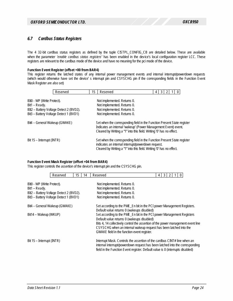
The 4 32-bit cardbus status registers as defined by the tuple CISTPL_CONFIG_CB are detailed below. These are available when the parameter ‘enable cardbus status registers’ has been enabled in the device’s local configuration register LCC. These registers are relevant to the cardbus mode of the device and have no meaning for the pci mode of the device. Function Event Register (offset +00 from BAR4) This register returns the latched states of any internal power management events and internal interrupt/powerdown requests (which would otherwise have set the device’ s interrupt pin and CSYSCHG pin if the corresponding fields in the Function Event Mask Register are also set)
Reserved 15 Reserved 4 3 2 1 0 BIt0 - WP (Write Protect). Not implemented. Returns 0. Bit1 – Ready. Not implemented. Returns 0. BIt2 – Battery Voltage Detect 2 (BVD2). Not implemented. Returns 0. Bit3 – Battery Voltage Detect 1 (BVD1) Not implemented. Returns 0. Bit4 – General Wakeup (GWAKE) Set when the corresponding field in the Function Present State register Indicates an internal ‘wakeup’ (Power Management Event) event. Cleared by Writing a “1” into this field. Writing ‘0’ has no effect. Bit 15 – Interrupt (INTR) Set when the corresponding field in the Function Present State register
indicates an internal interrupt/powerdown request. Cleared by Writing a “1” into this field. Writing ‘0’ has no effect. Function Event Mask Register (offset +04 from BAR4) This register controls the assertion of the device’s interrupt pin and the CSYSCHG pin.
Reserved 15 14 Reserved 4 3 2 1 0 BIt0 - WP (Write Protect). Not implemented. Returns 0. Bit1 – Ready. Not implemented. Returns 0. BIt2 – Battery Voltage Detect 2 (BVD2). Not implemented. Returns 0. Bit3 – Battery Voltage Detect 1 (BVD1) Not implemented. Returns 0. Bit4 – General Wakeup (GWAKE) Set according to the PME_En bit in the PCI power Management Registers. Default value returns 0 (wakeups disabled) Bit14 – Wakeup (WKUP) Set according to the PME_En bit in the PCI power Management Registers Default value returns 0 (wakeups disabled) Bits 4, 14 collectively control the assertion of the power management event line CSYSCHG when an internal wakeup request has been latched into the GWAKE field in the function event register. Bit 15 – Interrupt (INTR) Interrupt Mask. Controls the assertion of the cardbus CINT# line when an
internal interrupt/powerdown request has been latched into the corresponding field in the Function Event register. Default value is 0 (interrupts disabled)

Data Sheet Revision 1.1 Page 25
OXCB950
OXFORD SEMICONDUCTOR LTD.
Function Present State Register (offset +08 from BAR4) This register returns the internal (non-latched) states of the interrupt/powerdown requests and the internal (non-latched) state of the wakeup request.
Reserved 15 Reserved 4 3 2 1 0 BIt0 - WP (Write Protect). Not implemented. Returns 0. Bit1 – Ready. Not implemented. Returns 1. BIt2 – Battery Voltage Detect 2 (BVD2). Not implemented. Returns 1. Bit3 – Battery Voltage Detect 1 (BVD1) Not implemented. Returns 1. Bit4 – General Wakeup (GWAKE) Returns the present state (non-latched condition) of the internal power
management event request. Bit 15 – Interrupt (INTR) Returns the present state (non-latched condition) of the internal
interrupt/powerdown requests. Function Force Event Register (offset +0C from BAR4) This register does not physically exist. It provides the ability to simulate events by forcing values in the Function Event Register, primarily for debug purposes. The effect of a write to this register, will be reflected in the Function Event Register. However, if the function is active, other events on the cards may alter the contents of the function event register before it is read PC Card Standard, release 7.x.
Reserved 15 Reserved 4 3 2 1 0 BIt0 - WP (Write Protect). Not implemented. To be written with 0. Bit1 – Ready. Not implemented. To be written with 0. BIt2 – Battery Voltage Detect 2 (BVD2). Not implemented. To be written with 0. Bit3 – Battery Voltage Detect 1 (BVD1) Not implemented. To be written with 0. Bit4 – General Wakeup (GWAKE) Writing a ‘1’ to this field sets the GWAKE field in theFunction Event register,
without affecting the GWAKE field in the Function Present state register. Writing a ‘0’ has no effect. Bit 15 – Interrupt (INTR) Writing a ‘1’ to this field sets the INTR field in theFunction Event register,
without affecting the INTR field in the Function Present state register Writing a ‘0’ has no effect.

Data Sheet Revision 1.1 Page 26
OXCB950
OXFORD SEMICONDUCTOR LTD.
6.8 Cardbus Tuple Information
The cardbus information structure exists in the PCI configuration space at the user selectable location of either Dword 18 or Dword 32 and can occupy the entire PCI configuration space region from these specified locations upto Dword 63. By default, the Tuple information contained within the cardbus information structure (CIS) has been hardcoded into the device and has been designed to satisfy the requirements for most serial port based cardbus applications. For those manufacturers who would prefer to utilise their own tuple information into the cardbus information structure, for example to change the product ID and Manufacturers ID codes, then a facility is available that switches tuple access from the hardcoded area to a RAM that contains the user defined tuple information. Using the optional EEPROM to download data into the “CIS zone” results in the user defined tuple data being downloaded into this RAM and the RAM contents being then presented to the configuration software, once the OXCB950 device accepts the cardbus configuration accesses. The size of the RAM is 46 x 32bit data. This allows up to 184 bytes of Tuple information to be present in the PCI configuration space (from Dword18 to Dword63). By default, this RAM is set to read-only for configuration accesses. However, it is possible to enable configuration writes to this RAM by enabling the local configuration register LCC, bit 22 either through the EEPROM when downloading into the CIS zone or via transactions to this register bit. Only configuration writes will be possible to this RAM for experimentation purposes. Any new tuple data written directly into the RAM using cardbus transactions will not be automatically transferred to the EEPROM for subsequent downloads. The EEPROM will need to be updated using the controls in the local configuration register LCC, to mirror the data written directly to the RAM. The hardcoded (default) values in the cardbus information structure are as follows. This is the listing provided by Microsofts Tuple Utility DTPL.exe when operating on the Tuple information. NOTE : For user defined tuples, the tuple CISTPL_CONFIG_CB must indicate the cardbus status registers to be located at the (PCI) BAR4 in the PCI configuration space. PCI specifications define the base addresses as BAR0 0 – BAR5. Cardbus specifications define the base addresses as BAR1 – BAR6.
; Tuple Data for: (CISTPL_LINKTARGET) 13 03 43 49 53 ; Tuple Data for: (CISTPL_MANFID) 20 04 79 02 01 00 ; Tuple Data for: (CISTPL_CONFIG_CB) 04 06 03 00 05 00 00 00 ; Tuple Data for: (CISTPL_BAR) 07 06 11 00 F8 FF FF FF ; Tuple Data for: (CISTPL_BAR) 07 06 02 00 00 F0 FF FF ; Tuple Data for: (CISTPL_BAR) 07 06 13 00 F0 FF FF FF ; Tuple Data for: (CISTPL_BAR) 07 06 04 00 00 F0 FF FF ; Tuple Data for: (CISTPL_BAR) 07 06 05 00 00 F0 FF FF ; Tuple Data for: (CISTPL_CFTABLE_ENTRY_CB) 05 0C 40 B9 29 B5 1E 02 30 FF FF 04 C0 00 ; Tuple Data for: (CISTPL_VERS_1) 15 18 07 01 4F 58 53 45 4D 49 00 4F 58 43 42 39 35 30 00 52 65 76 20 41 00 FF ; Tuple Data for: (CISTPL_FUNCID) 21 02 02 00 ; Tuple Data for: (CISTPL_FUNCE) 22 04 00 02 0F 7F ; Tuple Data for: (CISTPL_DEVICE_OC) 1C 04 02 D2 08 FF ; Tuple Data for: (CISTPL_END) FF FF (None)
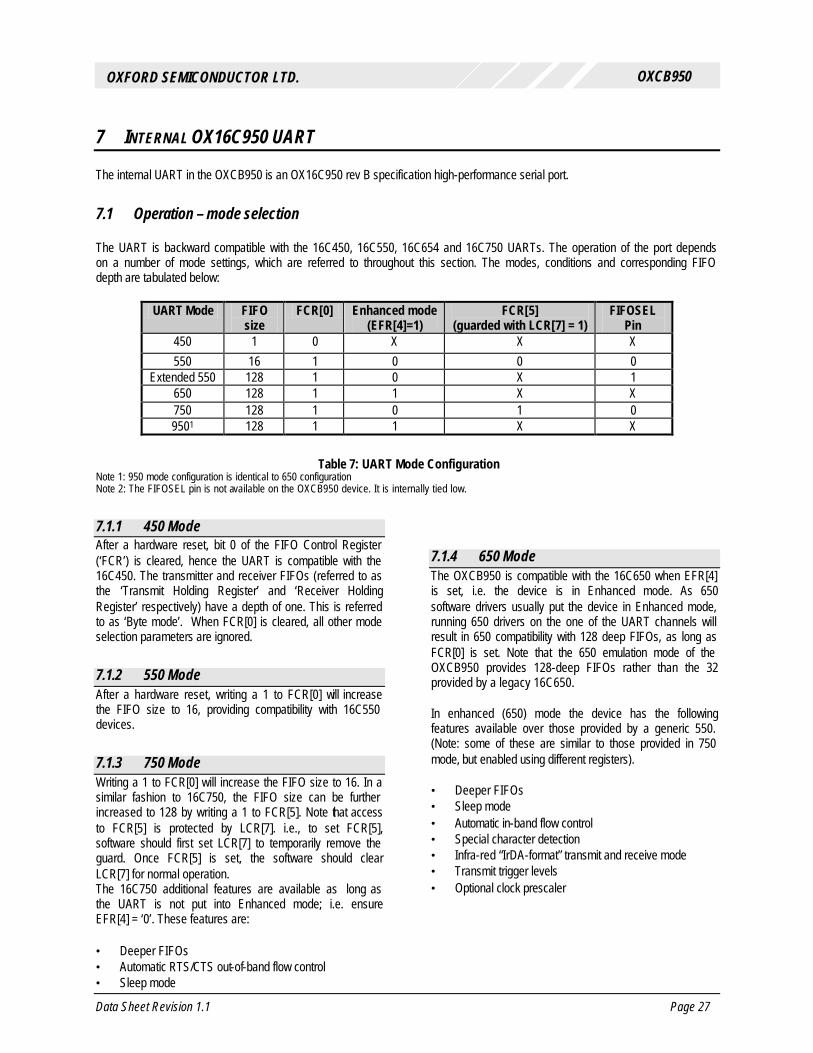
Data Sheet Revision 1.1 Page 27
OXCB950
OXFORD SEMICONDUCTOR LTD.
7 INTERNAL OX16C950 UART
The internal UART in the OXCB950 is an OX16C950 rev B specification high-performance serial port.
7.1 Operation – mode selection
The UART is backward compatible with the 16C450, 16C550, 16C654 and 16C750 UARTs. The operation of the port depends on a number of mode settings, which are referred to throughout this section. The modes, conditions and corresponding FIFO depth are tabulated below:
UART Mode FIFO size
FCR[0] Enhanced mode (EFR[4]=1)
FCR[5] (guarded with LCR[7] = 1)
FIFOSEL Pin
450 1 0 X X X 550 16 1 0 0 0
Extended 550 128 1 0 X 1 650 128 1 1 X X 750 128 1 0 1 0 9501 128 1 1 X X
Table 7: UART Mode Configuration Note 1: 950 mode configuration is identical to 650 configuration Note 2: The FIFOSEL pin is not available on the OXCB950 device. It is internally tied low.
7.1.1 450 Mode After a hardware reset, bit 0 of the FIFO Control Register (‘FCR’) is cleared, hence the UART is compatible with the 16C450. The transmitter and receiver FIFOs (referred to as the ‘Transmit Holding Register’ and ‘Receiver Holding Register’ respectively) have a depth of one. This is referred to as ‘Byte mode’. When FCR[0] is cleared, all other mode selection parameters are ignored.
7.1.2 550 Mode After a hardware reset, writing a 1 to FCR[0] will increase the FIFO size to 16, providing compatibility with 16C550 devices.
7.1.3 750 Mode Writing a 1 to FCR[0] will increase the FIFO size to 16. In a similar fashion to 16C750, the FIFO size can be further increased to 128 by writing a 1 to FCR[5]. Note that access to FCR[5] is protected by LCR[7]. i.e., to set FCR[5], software should first set LCR[7] to temporarily remove the guard. Once FCR[5] is set, the software should clear LCR[7] for normal operation. The 16C750 additional features are available as long as the UART is not put into Enhanced mode; i.e. ensure EFR[4] = ‘0’. These features are: • Deeper FIFOs • Automatic RTS/CTS out-of-band flow control • Sleep mode
7.1.4 650 Mode The OXCB950 is compatible with the 16C650 when EFR[4] is set, i.e. the device is in Enhanced mode. As 650 software drivers usually put the device in Enhanced mode, running 650 drivers on the one of the UART channels will result in 650 compatibility with 128 deep FIFOs, as long as FCR[0] is set. Note that the 650 emulation mode of the OXCB950 provides 128-deep FIFOs rather than the 32 provided by a legacy 16C650. In enhanced (650) mode the device has the following features available over those provided by a generic 550. (Note: some of these are similar to those provided in 750 mode, but enabled using different registers). • Deeper FIFOs • Sleep mode • Automatic in-band flow control • Special character detection • Infra-red “IrDA-format” transmit and receive mode • Transmit trigger levels • Optional clock prescaler

Data Sheet Revision 1.1 Page 28
OXCB950
OXFORD SEMICONDUCTOR LTD.
7.1.5 950 Mode The additional features offered in 950 mode generally only apply when the UART is in Enhanced mode (EFR[4]=’1’). Provided FCR[0] is set, in Enhanced mode the FIFO size is 128. Note that 950 mode configuration is identical to that of 650 mode, however additional 950 specific features are enabled using the Additional Control Register ‘ACR’ (see section 7.11.3). In addition to larger FIFOs and higher baud rates, the enhancements of the 950 mode over 650 emulation mode are: • Selectable arbitrary trigger levels for the receiver and
transmitter FIFO interrupts • Improved automatic flow control using selectable
arbitrary thresholds • DSR#/DTR# automatic flow control • Transmitter and receiver can be optionally disabled • Software reset of device • Readable FIFO fill levels • Optional generation of an RS-485 buffer enable signal • Four-byte device identification (0x16C95005) • Readable status for automatic in-band and out-of-
band flow control • External 1x clock modes (see section 0) • Flexible “M+N/8” clock prescaler (see section 7.10.2) • Programmable sample clock to allow data rates up to
15 Mbps (see section 7.10.3). • 9-bit data mode • Readable FCR register The 950 trigger levels are enabled when ACR[5] is set where bits 4 to 7 of FCR are ignored. Then arbitrary trigger levels can be defined in RTL, TTL, FCL and FCH registers (see section 7.11). The Additional Status Register (‘ASR’) offers flow control status for the local and remote
transmitters. FIFO levels are readable using RFL and TFL registers. The UART has a flexible prescaler capable of dividing the system clock by any value between 1 and 31.875 in steps of 0.125. It divides the system clock by an arbitrary value in “M+N/8” format, where M and N are 5- and 3-bit binary numbers programmed in CPR[7:3] and CPR[2:0] respectively. This arrangement offers a great deal of flexibility when choosing an input clock frequency to synthesise arbitrary baud rates. The default division value is 4 to provide backward compatibility with 16C650 devices. The user may apply an external 1x (or Nx) clock for the transmitter and receiver to the RI# and DSR# pin respectively. The transmitter clock may instead be asserted on the DTR# pin. The external clock options are selected through the CKS register (offset 0x02 of ICR). It is also possible to define the over-sampling rate used by the transmitter and receiver clocks. The 16C450/16C550 and compatible devices employ 16 times over-sampling, where there are 16 clock cycles per bit. However the 950 UART can employ any over-sampling rate from 4 to 16 by programming the TCR register. This allows the data rates to be increased to 460.8 Kbps using a 1.8432MHz clock, or 15 Mbps using a 60 MHz clock. The default value after a reset for this register is 0x00, which corresponds to a 16 cycle sampling clock. Writing 0x01, 0x02 or 0x03 will also result in a 16 cycle sampling clock. To program the value to any value from 4 to 15 it is necessary to write this value into the TCR i.e. to set the device to a 13 cycle sampling clock it would be necessary to write 0x0D to TCR. For further information see section 7.10.3 The UART also offers 9-bit data frames for multi-drop industrial applications.
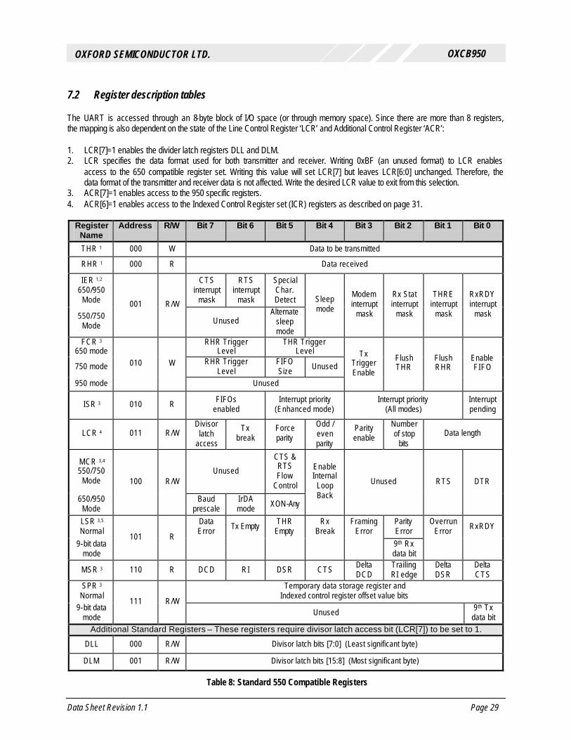
Data Sheet Revision 1.1 Page 29
OXCB950
OXFORD SEMICONDUCTOR LTD.
7.2 Register description tables
The UART is accessed through an 8-byte block of I/O space (or through memory space). Since there are more than 8 registers, the mapping is also dependent on the state of the Line Control Register ‘LCR’ and Additional Control Register ‘ACR’: 1. LCR[7]=1 enables the divider latch registers DLL and DLM. 2. LCR specifies the data format used for both transmitter and receiver. Writing 0xBF (an unused format) to LCR enables
access to the 650 compatible register set. Writing this value will set LCR[7] but leaves LCR[6:0] unchanged. Therefore, the data format of the transmitter and receiver data is not affected. Write the desired LCR value to exit from this selection.
3. ACR[7]=1 enables access to the 950 specific registers. 4. ACR[6]=1 enables access to the Indexed Control Register set (ICR) registers as described on page 31.
Register Name
Address R/W Bit 7 Bit 6 Bit 5 Bit 4 Bit 3 Bit 2 Bit 1 Bit 0
THR 1 000 W Data to be transmitted
RHR 1 000 R Data received
IER 1,2 650/950
Mode
CTS interrupt
mask
RTS interrupt
mask
Special Char. Detect
550/750 Mode
001 R/W
Unused Alternate
sleep mode
Sleep mode
Modem interrupt
mask
Rx Stat interrupt
mask
THRE interrupt
mask
RxRDY interrupt
mask
FCR 3 650 mode
RHR Trigger Level
THR Trigger Level
750 mode RHR Trigger Level
FIFO Size Unused
950 mode
010 W
Unused
Tx Trigger Enable
Flush THR
Flush RHR
Enable FIFO
ISR 3 010 R FIFOs enabled
Interrupt priority (Enhanced mode)
Interrupt priority (All modes)
Interrupt pending
LCR 4 011 R/W Divisor
latch access
Tx break
Force parity
Odd / even parity
Parity enable
Number of stop
bits Data length
MCR 3,4
550/750 Mode
Unused
CTS & RTS Flow
Control
650/950 Mode
100 R/W
Baud prescale
IrDA mode XON-Any
Enable Internal
Loop Back
Unused RTS DTR
LSR 3,5 Normal
Data Error Tx Empty THR
Empty Rx
Break Framing
Error Parity Error
Overrun Error RxRDY
9-bit data mode
101 R 9th Rx
data bit
MSR 3 110 R DCD RI DSR CTS Delta DCD
Trailing RI edge
Delta DSR
Delta CTS
SPR 3 Normal
Temporary data storage register and Indexed control register offset value bits
9-bit data mode
111 R/W Unused 9th Tx
data bit Additional Standard Registers – These registers require divisor latch access bit (LCR[7]) to be set to 1.
DLL 000 R/W Divisor latch bits [7:0] (Least significant byte)
DLM 001 R/W Divisor latch bits [15:8] (Most significant byte)
Table 8: Standard 550 Compatible Registers

Data Sheet Revision 1.1 Page 30
OXCB950
OXFORD SEMICONDUCTOR LTD.
Register
Name Address R/W Bit 7 Bit 6 Bit 5 Bit 4 Bit 3 Bit 2 Bit 1 Bit 0
To access these registers LCR must be set to 0xBF EFR 010 R/W CTS
flow control
RTS Flow
control
Special char
detect
Enhance mode
In-band flow control mode
XON1
100 R/W XON Character 1
9-bit mode Special character 1 XON2
101 R/W XON Character 2
9-bit mode Special Character 2 XOFF1
110 R/W XOFF Character 1
9-bit mode Special character 3 XOFF2
111 R/W XOFF Character 2
9-bit mode Special character 4
Table 9: 650 Compatible Registers
Register
Name Address R/W Bit 7 Bit 6 Bit 5 Bit 4 Bit 3 Bit 2 Bit 1 Bit 0
ASR 1,6,7
001 R/W 7 Tx Idle
FIFO size
FIFO- SEL
Special Char
Detect
DTR RTS Remote Tx
Disabled
Tx Disabled
RFL 6 011 R Number of characters in the receiver FIFO
TFL 3,6 100 R Number of characters in the transmitter FIFO
ICR 3,8,9
101 R/W Data read/written depends on the value written to the SPR prior to the access of this register (see Table 11)
Table 10: 950 Specific Registers
Register access notes: Note 1: Requires LCR[7] = 0 Note 2: Requires ACR[7] = 0 Note 3: Requires that last value written to LCR was not 0xBF Note 4: To read this register ACR[7] must be = 0 Note 5: To read this register ACR[6] must be = 0 Note 6: Requires ACR[7] = 1 Note 7: Only bits 0 and 1 of this register can be written Note 8: To read this register ACR[6] must be = 1 Note 9: This register acts as a window through which to read and write registers in the Indexed Control Register set

Data Sheet Revision 1.1 Page 31
OXCB950
OXFORD SEMICONDUCTOR LTD.
Register
Name SPR
Offset 10 R/W Bit 7 Bit 6 Bit 5 Bit 4 Bit 3 Bit 2 Bit 1 Bit 0
Indexed Control Register Set ACR 0x00 R/W Addit-
ional Status
Enable
ICR Read
Enable
950 Trigger Level
Enable
DTR definition and control
Auto DSR Flow
Control Enable
Tx Disable
Rx Disable
CPR 0x01 R/W 5 Bit “integer” part of clock prescaler
3 Bit “fractional” part of clock prescaler
TCR 0x02 R/W Unused 4 Bit N-times clock selection bits [3:0]
CKS 0x03 R/W Tx 1x Mode
Tx CLK Select
BDOUT on DTR
DTR 1x Tx CLK
Rx 1x Mode
0 Receiver Clock Sel[1:0]
TTL 0x04 R/W Unused Transmitter Interrupt Trigger Level (0-127)
RTL 0x05 R/W Unused Receiver Interrupt Trigger Level (1-127)
FCL 0x06 R/W Unused Automatic Flow Control Lower Trigger Level (0-127)
FCH 0x07 R/W Unused Automatic Flow Control Higher Trigger level (1-127)
ID1 0x08 R Hardwired ID byte 1 (0x16)
ID2 0x09 R Hardwired ID byte 1 (0xC9)
ID3 0x0A R Hardwired ID byte 1 (0x50)
REV 0x0B R Hardwired revision byte (0x05)
CSR 0x0C W Writing 0x00 to this register will reset the UART (Except the CKS and CKA registers)
NMR 0x0D R/W Unused 9th Bit SChar 4
9th Bit SChar 3
9th Bit SChar 2
9th Bit SChar 1
9th-bit Int. En.
9 Bit Enable
MDM 0x0E R/W 0 0 SIN wakeup disable
Modem Wakeup Disable
∆ DCD Wakeup disable
Trailing RI edge disable
∆ DSR Wakeup disable
∆ CTS Wakeup disable
RFC 0X0F R FCR[7] FCR[6] FCR[5] FCR[4] FCR[3] FCR[2] FCR[1] FCR[0] GDS 0X10 R Unused Good
Data Status
DMS 0x11 R/W Force TxRdy inactive
Force RxRdy inactive
Unused
TxRdy status ( R )
RxRdy status ( R )
PIDX 0x12 R Hardwired Port Index ( 0x00 ) CKA 0x13 R/W
Unused Invert DTR signal
Invert internal tx clock
Invert internal rx clock
Table 11: Indexed Control Register Set Note 10: The SPR offset column indicates the value that must be written into SPR prior to reading / writing any of the Indexed Control Registers via ICR.
Offset values not listed in the table are reserved for future use and must not be used. To read or write to any of the Indexed Controlled Registers use the following procedure: Writing to ICR registers: Ensure that the last value written to LCR was not 0xBF (reserved for 650 compatible register access value). Write the desired offset to SPR (address 111b). Write the desired value to ICR (address 101b).

Data Sheet Revision 1.1 Page 32
OXCB950
OXFORD SEMICONDUCTOR LTD.
Reading from ICR registers: Ensure that the last value written to LCR was not 0xBF (see above). Write 0x00 offset to SPR to select ACR. Set bit 6 of ACR (ICR read enable) by writing x1xxxxxxb to address 101b. Ensure that other bits in ACR are not changed. (Software drivers should keep a copy of the contents of the ACR elsewhere since reading ICR involves overwriting ACR!) Write the desired offset to SPR (address 111b). Read the desired value from ICR (address 101b). Write 0x00 offset to SPR to select ACR. Clear bit 6 of ACR bye writing x0xxxxxxb to ICR, thus enabling access to standard registers again.
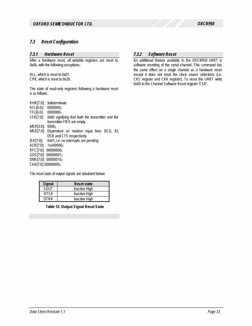
Data Sheet Revision 1.1 Page 33
OXCB950
OXFORD SEMICONDUCTOR LTD.
7.3 Reset Configuration
7.3.1 Hardware Reset After a hardware reset, all writable registers are reset to 0x00, with the following exceptions: DLL, which is reset to 0x01. CPR, which is reset to 0x20. The state of read-only registers following a hardware reset is as follows: RHR[7:0]: Indeterminate RFL[6:0]: 00000002
TFL[6:0]: 00000002
LSR[7:0]: 0x60 signifying that both the transmitter and the transmitter FIFO are empty
MSR[3:0]: 00002
MSR[7:4]: Dependent on modem input lines DCD, RI, DSR and CTS respectively
ISR[7:0]: 0x01, i.e. no interrupts are pending ASR[7:0]: 1xx000002
RFC[7:0]: 000000002
GDS[7:0]: 000000012
DMS[7:0]: 000000102
CKA[7:0]: 000000002
The reset state of output signals are tabulated below:
Signal Reset state SOUT Inactive High RTS# Inactive High DTR# Inactive High
Table 12: Output Signal Reset State
7.3.2 Software Reset An additional feature available in the OXCB950 UART is software resetting of the serial channel. This command has the same effect on a single channel as a hardware reset except it does not reset the clock source selections (i.e. CKS register and CKA register). To reset the UART write 0x00 to the Channel Software Reset register ‘CSR’.

Data Sheet Revision 1.1 Page 34
OXCB950
OXFORD SEMICONDUCTOR LTD.
7.4 Transmitter and receiver FIFOs
Both the transmitter and receiver have associated holding registers (FIFOs), referred to as the transmitter holding register (THR) and receiver holding register (RHR) respectively. In normal operation, when the transmitter finishes transmitting a byte it will remove the next data from the top of the THR and proceed to transmit it. If the THR is empty, it will wait until data is written into it. If THR is empty and the last character being transmitted has been completed (i.e. the transmitter shift register is empty) the transmitter is said to be idle. Similarly, when the receiver finishes receiving a byte, it will transfer it to the bottom of the RHR. If the RHR is full, an overrun condition will occur (see section 7.5.3). Data is written into the bottom of the THR queue and read from the top of the RHR queue completely asynchronously to the operation of the transmitter and receiver. The size of the FIFOs is dependent on the setting of the FCR register. When in Byte mode, these FIFOs only accept one byte at a time before indicating that they are full; this is compatible with the 16C450. When in a FIFO mode, the size of the FIFOs is either 16 (compatible with the 16C550) or 128. Data written to the THR when it is full is lost. Data read from the RHR when it is empty is invalid. The empty or full status of the FIFOs are indicated in the Line Status Register ‘LSR’ (see section 7.5.3). Interrupts are generated when the UART is ready for data transfer to/from the FIFOs. The number of items in each FIFO may also be read back from the transmitter FIFO level (TFL) and receiver FIFO level (RFL) registers (see section 7.11.2).
7.4.1 FIFO Control Register ‘FCR’ FIFO setup: FCR[0]: Enable FIFO mode logic 0 ⇒ Byte mode. logic 1 ⇒ FIFO mode. This bit should be enabled before setting the FIFO trigger levels. FCR[1]: Flush RHR logic 0 ⇒ No change. logic 1 ⇒ Flushes the contents of the RHR This is only operative when already in a FIFO mode. The RHR is automatically flushed whenever changing between
Byte mode and a FIFO mode. This bit will return to zero after clearing the FIFOs. FCR[2]: Flush THR logic 0 ⇒ No change. logic 1 ⇒ Flushes the contents of the THR, in the same manner as FCR[1] does for the RHR. THR Trigger levels: FCR[3]: Tx trigger level enable logic 0 ⇒ Transmit trigger levels enabled logic 1 ⇒ Transmit trigger levels disabled When FCR[3]=0, the transmitter trigger level is always set to 1, thus ignoring FCR[5:4]. Alternatively, 950-mode trigger levels can be set using ACR[5]. FCR[5:4]: Compatible trigger levels 450, 550 and extended 550 modes: The transmitter interrupt trigger levels are set to 1 and FCR[5:4] are ignored. 650 mode: In 650 mode the transmitter interrupt trigger levels can be set to the following values:
FCR[5:4] Transmit Interrupt Trigger level 00 16 01 32 10 64 11 112
Table 13: Transmit Interrupt Trigger Levels These levels only apply when in Enhanced mode and when FCR[3] is set, otherwise the trigger level is set to 1. A transmitter empty interrupt will be generated (if enabled) if the TFL falls below the trigger level. 750 Mode: In 750 compatible mode, transmitter trigger level is set to 1, FCR[4] is unused and FCR[5] defines the FIFO depth as follows: FCR[5]=0: FIFO size is 16 bytes. FCR[5]=1: FIFO size is 128 bytes. In non-Enhanced mode and when FIFOSEL pin is low (tied low internally on the OXCB950) FCR[5] is writable only when LCR[7] is set. Note that in Enhanced mode, the FIFO size is increased to 128 bytes when FCR[0] is set.

Data Sheet Revision 1.1 Page 35
OXCB950
OXFORD SEMICONDUCTOR LTD.
950 mode: Setting ACR[5]=1 enables 950-mode trigger levels set using the TTL register (see section 7.11.4), FCR[5:4] are ignored. RHR trigger levels FCR[7:6]: Compatible Trigger levels 450, 550, extended 550, 650 and 750 modes: The receiver FIFO trigger levels are defined using FCR[7:6]. The interrupt trigger level and upper flow control trigger level where appropriate are defined by L1 in the table below. L2 defines the lower flow control trigger level. Separate upper and lower flow control trigger levels introduce a hysteresis element in in-band and out-of-band flow control (see section 7.9). In Byte mode (450 mode) the trigger levels are all set to 1.
950 mode: In similar fashion to for transmitter trigger levels, setting ACR[5]=1 enables 950-mode receiver trigger levels. FCR[7:6] are ignored.
Mode 550
FIFO Size 16 Ext. 550 / 750 FIFO Size 128
650 FIFO Size 128
FCR [7:6]
L1 L2 L1 L2 L1 L2 00 1 n/a 1 1 16 1 01 4 n/a 32 1 32 16 10 8 n/a 64 1 112 32 11 14 n/a 112 1 120 112
Table 14: Compatible Receiver Trigger Levels A receiver data interrupt will be generated (if enabled) if the Receiver FIFO Level (‘RFL’) reaches the upper trigger level.
7.5 Line Control & Status
7.5.1 False Start Bit Detection On the falling edge of a start bit, the receiver will wait for 1/2 bit and re-synchronise the receiver’s sampling clock onto the centre of the start bit. The start bit is valid if the SIN line is still low at this mid-bit sample and the receiver will proceed to read in a data character. Verifying the start bit prevents noise generating spurious character generation. Once the first stop bit has been sampled, the received data is transferred to the RHR and the receiver will then wait for a low transition on SIN (signifying the next start bit). The receiver will continue receiving data even if the RHR is full or the receiver has been disabled (see section 7.11.3) in order to maintain framing synchronisation. The only difference is that the received data does not get transferred to the RHR.
7.5.2 Line Control Register ‘LCR’ The LCR specifies the data format that is common to both transmitter and receiver. Writing 0xBF to LCR enables access to the EFR, XON1, XOFF1, XON2 and XOFF2, DLL and DLM registers. This value (0xBF) corresponds to an unused data format. Writing the value 0xBF to LCR will set LCR[7] but leaves LCR[6:0] unchanged. Therefore, the data format of the transmitter and receiver data is not
affected. Write the desired LCR value to exit from this selection. LCR[1:0]: Data length LCR[1:0] Determines the data length of serial characters. Note however, that these values are ignored in 9-bit data framing mode, i.e. when NMR[0] is set.
LCR[1:0] Data length 00 5 bits 01 6 bits 10 7 bits 11 8 bits
Table 15: LCR Data Length Configuration LCR[2]: Number of stop bits LCR[2] defines the number of stop bits per serial character.
LCR[2] Data length No. stop bits
0 5,6,7,8 1 1 5 1.5 1 6,7,8 2
Table 16: LCR Stop Bit Number Configuration
Data Sheet Revision 1.1 Page 36
OXCB950
OXFORD SEMICONDUCTOR LTD.
LCR[5:3]: Parity type The selected parity type will be generated during transmission and checked by the receiver, which may produce a parity error as a result. In 9-bit mode parity is disabled and LCR[5:3] is ignored.
LCR[5:3] Parity type xx0 No parity bit 001 Odd parity bit 011 Even parity bit 101 Parity bit forced to 1 111 Parity bit forced to 0
Table 17: LCR Parity Configuration LCR[6]: Transmission break logic 0 ⇒ Break transmission disabled. logic 1 ⇒ Forces the transmitter data output SOUT low to alert the communication terminal, or send zeros in IrDA mode. It is the responsibility of the software driver to ensure that the break duration is longer than the character period for it to be recognised remotely as a break rather than data. LCR[7]: Divisor latch enable logic 0 ⇒ Access to DLL and DLM registers disabled. logic 1 ⇒ Access to DLL and DLM registers enabled.
7.5.3 Line Status Register ‘LSR’ This register provides the status of data transfer to CPU. LSR[0]: RHR data available logic 0 ⇒ RHR is empty : no data available logic 1 ⇒ RHR is not empty: data is available to be read. LSR[1]: RHR overrun error logic 0 ⇒ No overrun error. logic 1 ⇒ Data was received when the RHR was full. An
overrun error has occurred. The error is flagged when the data would normally have been transferred to the RHR.
LSR[2]: Received data parity error logic 0 ⇒ No parity error in normal mode or 9th bit of
received data is ‘0’ in 9-bit mode. logic 1 ⇒ Data has been received that did not have
correct parity in normal mode or 9th bit of received data is ‘1’ in 9-bit mode.
The Parity error flag will be set when the data item in error is at the top of the RHR and cleared following a read of the LSR. In 9-bit mode LSR[2] is no longer a flag and corresponds to the 9th bit of the received data in RHR. LSR[3]: Received data framing error logic 0 ⇒ No framing error. logic 1 ⇒ Data has been received with an invalid stop bit. This status bit is set and cleared in the same manner as LSR[2]. When a framing error occurs, the UART will try to re-synchronise by assuming that the error was due to sampling the start bit of the next data item. LSR[4]: Received break error logic 0 ⇒ No receiver break error. logic 1 ⇒ The receiver received a break. A break condition occurs when the SIN line goes low (normally signifying a start bit) and stays low throughout the start, data, parity and first stop bit. (Note that the SIN line is sampled at the bit rate). One zero character with associated break flag set will be transferred to the RHR and the receiver will then wait until the SIN line returns high. The LSR[4] break flag will be set when this data item gets to the top of the RHR and it is cleared following a read of the LSR. LSR[5]: THR empty logic 0 ⇒ Transmitter FIFO (THR) is not empty. logic 1 ⇒ Transmitter FIFO (THR) is empty. LSR[6]: Transmitter and THR empty logic 0 ⇒ The transmitter is not idle logic 1 ⇒ THR is empty and the transmitter has
completed the character in shift register and is in idle mode. (I.e. set whenever the transmitter shift register and the THR are both empty.)
LSR[7]: Receiver data error logic 0 ⇒ Either there are no receiver data errors in the
FIFO or it was cleared by a read of LSR. logic 1 ⇒ At least one parity error, framing error or break
indication in the FIFO. In 450 mode LSR[7] is permanently cleared, otherwise this bit will be set when an erroneous character is transferred from the receiver to the RHR. It is cleared when the LSR is read. Note that in 16C550 this bit is only cleared when all of the erroneous data are removed from the FIFO. In 9-bit data framing mode parity is permanently disabled, so this bit is not affected by LSR[2].

Data Sheet Revision 1.1 Page 37
OXCB950
OXFORD SEMICONDUCTOR LTD.
7.6 Interrupts & Sleep Mode
The serial channel interrupts are asserted on the PCI INTA# pin. The interrupts can be enabled or disabled using the GIS register interrupt mask (see section 6.4.4) and the IER register. Unlike generic 16C550 devices, the interrupt can not be disabled using the implementation-specific MCR[3].
7.6.1 Interrupt Enable Register ‘IER’ Serial channel interrupts are enabled using the Interrupt Enable Register (‘IER’). IER[0]: Receiver data available interrupt mask logic 0 ⇒ Disable the receiver ready interrupt. logic 1 ⇒ Enable the receiver ready interrupt. IER[1]: Transmitter empty interrupt mask logic 0 ⇒ Disable the transmitter empty interrupt. logic 1 ⇒ Enable the transmitter empty interrupt. IER[2]: Receiver status interrupt Normal mode: logic 0 ⇒ Disable the receiver status interrupt. logic 1 ⇒ Enable the receiver status interrupt. 9-bit data mode: logic 0 ⇒ Disable receiver status and address bit
interrupt. logic 1 ⇒ Enable receiver status and address bit
interrupt. In 9-bit mode (i.e. when NMR[0] is set), reception of a character with the address-bit (i.e. 9th bit) set can generate a level 1 interrupt if IER[2] is set. IER[3]: Modem status interrupt mask logic 0 ⇒ Disable the modem status interrupt. logic 1 ⇒ Enable the modem status interrupt. IER[4]: Sleep mode logic 0 ⇒ Disable sleep mode. logic 1 ⇒ Enable sleep mode whereby the internal clock
of the channel is switched off. Sleep mode is described in section 7.6.4. IER[5]: Special character interrupt mask or alternate sleep mode 9-bit data framing mode: logic 0 ⇒ Disable the received special character interrupt. logic 1 ⇒ Enable the received special character interrupt.
In 9-bit data mode, The receiver can detect up to four special characters programmed in the Special Character Registers (see map on page 30). When IER[5] is set, a level 5 interrupt is asserted when the receiver character matches one of the values programmed. 650/950 modes (non-9-bit data framing): logic 0 ⇒ Disable the special character receive interrupt. logic 1 ⇒ Enable the special character receive interrupt. In 16C650 compatible mode when the device is in Enhanced mode (EFR[4]=1), this bit enables the detection of special characters. It enables both the detection of XOFF characters (when in-band flow control is enabled via EFR[3:0]) and the detection of the XOFF2 special character (when enabled via EFR[5]). 750 mode (non-9-bit data framing): logic 0 ⇒ Disable alternate sleep mode. logic 1 ⇒ Enable alternate sleep mode whereby the
internal clock of the channel is switched off. In 16C750 compatible mode (i.e. non-Enhanced mode), this bit is used an alternate sleep mode and has the same effect as IER[4]. IER[6]: RTS interrupt mask logic 0 ⇒ Disable the RTS interrupt. logic 1 ⇒ Enable the RTS interrupt. This enable is only operative in Enhanced mode (EFR[4]=1). In non-Enhanced mode, RTS interrupt is permanently enabled IER[7]: CTS interrupt mask logic 0 ⇒ Disable the CTS interrupt. logic 1 ⇒ Enable the CTS interrupt. This enable is only operative in Enhanced mode (EFR[4]=1). In non-Enhanced mode, CTS interrupt is permanently enabled.
Data Sheet Revision 1.1 Page 38
OXCB950
OXFORD SEMICONDUCTOR LTD.
7.6.2 Interrupt Status Register ‘ISR’ The source of the highest priority interrupt pending is indicated by the contents of the Interrupt Status Register ‘ISR’. There are nine sources of interrupt at six levels of priority (1 is the highest) as shown in Table 18.
Level Interrupt source ISR[5:0] see note 3
- No interrupt pending 1 000001 1 Receiver status error or
Address-bit detected in 9-bit mode 000110
2a Receiver data available 000100 2b Receiver time-out 001100 3 Transmitter THR empty 000010 4 Modem status change 000000 5 2 In-band flow control XOFF or
Special character (XOFF2) or Special character 1, 2, 3 or 4 or bit 9 set in 9-bit mode
010000
6 2 CTS or RTS change of state 100000
Table 18: Interrupt Status Identification Codes Note1: ISR[0] indicates whether any interrupts are pending. Note2: Interrupts of priority levels 5 and 6 cannot occur unless the
UART is in Enhanced mode. Note3: ISR[5] is only used in 650 & 950 modes. In 750 mode, it is ‘0’
when FIFO size is 16 and ‘1’ when FIFO size is 128. In all other modes it is permanently set to 0
7.6.3 Interrupt Description Level 1: Receiver status error interrupt (ISR[5:0]=’000110’): Normal (non-9-bit) mode: This interrupt is active whenever any of LSR[1], LSR[2], LSR[3] or LSR[4] are set. These flags are cleared following a read of the LSR. This interrupt is masked with IER[2]. 9-bit mode: This interrupt is active whenever any of LSR[1], LSR[2], LSR[3] or LSR[4] are set. The receiver error interrupt due to LSR[1], LSR[3] and LSR[4] is masked with IER[3]. The ‘address-bit’ received interrupt is masked with NMR[1]. The software driver can differentiate between receiver status error and received address-bit (9th data bit) interrupt by examining LSR[1] and LSR[7]. In 9-bit mode LSR[7] is only set when LSR[3] or LSR[4] is set and it is not affected by LSR[2] (i.e. 9th data bit).
Level 2a: Receiver data available interrupt (ISR[5:0]=’000100’): This interrupt is active whenever the receiver FIFO level is above the interrupt trigger level. Level 2b: Receiver time-out interrupt (ISR[5:0]=’001100’): A receiver time-out event, which may cause an interrupt, will occur when all of the following conditions are true: • The UART is in a FIFO mode • There is data in the RHR. • There has been no read of the RHR for a period of
time greater than the time-out period. • There has been no new data written into the RHR for
a period of time greater than the time-out period. The time-out period is four times the character period (including start and stop bits) measured from the centre of the first stop bit of the last data item received.
Reading the first data item in RHR clears this interrupt. Level 3: Transmitter empty interrupt (ISR[5:0]=’000010’): This interrupt is set when the transmit FIFO level falls below the trigger level. It is cleared on an ISR read of a level 3 interrupt or by writing more data to the THR so that the trigger level is exceeded. Note that when 16C950 mode trigger levels are enabled (ACR[5]=1) and the transmitter trigger level of zero is selected (TTL=0x00), a transmitter empty interrupt will only be asserted when both the transmitter FIFO and transmitter shift register are empty and the SOUT line has returned to idle marking state. Level 4: Modem change interrupt (ISR[5:0]=’000000’): This interrupt is set by a modem change flag (MSR[0], MSR[1], MSR[2] or MSR[3]) becoming active due to changes in the input modem lines. This interrupt is cleared following a read of the MSR. Level 5: Receiver in-band flow control (XOFF) detect interrupt, Receiver special character (XOFF2) detect interrupt, Receiver special character 1, 2, 3 or 4 interrupt or 9th Bit set interrupt in 9-bit mode (ISR[5:0]=’010000’): A level 5 interrupt can only occur in Enhanced-mode when any of the following conditions are met: • A valid XOFF character is received while in-band flow
control is enabled. • A received character matches XOFF2 while special
character detection is enabled, i.e. EFR[5]=1. • A received character matches special character 1, 2, 3
or 4 in 9-bit mode (see section 7.11.9). It is cleared on an ISR read of a level 5 interrupt.
Data Sheet Revision 1.1 Page 39
OXCB950
OXFORD SEMICONDUCTOR LTD.
Level 6: CTS or RTS changed interrupt (ISR[5:0]=’100000’): This interrupt is set whenever any of the CTS# or RTS# pins changes state from low to high. It is cleared on an ISR read of a level 6 interrupt.
7.6.4 Sleep Mode For a channel to go into sleep mode, all of the following conditions must be met: • Sleep mode enabled (IER[4]=1 in 650/950 modes, or
IER[5]=1 in 750 mode): • The transmitter is idle, i.e. the transmitter shift register
and FIFO are both empty. • SIN is high. • The receiver is idle. • The receiver FIFO is empty (LSR[0]=0).
• The UART is not in loopback mode (MCR[4]=0). • Changes on modem input lines have been
acknowledged (i.e. MSR[3:0]=0000). • No interrupts are pending. A read of IER[4] (or IER[5] if a 1 was written to that bit instead) shows whether the power-down request was successful. The UART will retain its programmed state whilst in power-down mode. The channel will automatically exit power-down mode when any of the conditions 1 to 7 becomes false. It may be woken manually by clearing IER[4] (or IER[5] if the alternate sleep mode is enabled). Sleep mode operation is not available in IrDA mode.
7.7 Modem Interface
7.7.1 Modem Control Register ‘MCR’ MCR[0]: DTR logic 0 ⇒ Force DTR# output to inactive (high). logic 1 ⇒ Force DTR# output to active (low). Note that DTR# can be used for automatic out-of-band flow control when enabled using ACR[4:3] (see section 7.11.3). MCR[1]: RTS logic 0 ⇒ Force RTS# output to inactive (high). logic 1 ⇒ Force RTS# output to active (low). Note that RTS# can be used for automatic out-of-band flow control when enabled using EFR[6] (see section 7.9.4). MCR[2]: OUT1 logic 0 ⇒ Force OUT1# output low when loopback mode
is disabled. logic 1 ⇒ Force OUT1# output high. MCR[3]: OUT2/External interrupt enable logic 0 ⇒ Force OUT2# output low when loopback mode
is disabled. If INT_SEL# is low the external interrupt is in high-impedance state when MCR[3] is cleared. If INT_SEL# is high MCR[3] does not affect the interrupt.
logic 1 ⇒ Force OUT2# output high. If INT_SEL# is low the external interrupt is enabled and operating in normal active (forcing) mode when MCR[3] is high. If INT_SEL# is high MCR[3] does not affect the interrupt.
MCR[4]: Loopback mode logic 0 ⇒ Normal operating mode. logic 1 ⇒ Enable local loop-back mode (diagnostics). In local loop-back mode, the transmitter output (SOUT) and the four modem outputs (DTR#, RTS#, OUT1# and OUT2#) are set in-active (high), and the receiver inputs SIN, CTS#, DSR#, DCD#, and RI# are all disabled. Internally the transmitter output is connected to the receiver input and DTR#, RTS#, OUT1# and OUT2# are connected to modem status inputs DSR#, CTS#, RI# and DCD# respectively. In this mode, the receiver and transmitter interrupts are fully operational. The modem control interrupts are also operational, but the interrupt sources are now the lower four bits of the Modem Control Register instead of the four modem status inputs. The interrupts are still controlled by the IER. MCR[5]: Enable XON-Any in Enhanced mode or enable out-of-band flow control in non-Enhanced mode 650/950 (enhanced) modes: logic 0 ⇒ XON-Any is disabled. logic 1 ⇒ XON-Any is enabled. In enhanced mode (EFR[4]=1), this bit enables the Xon-Any operation. When Xon-Any is enabled, any received data will be accepted as a valid XON (see in-band flow control, section 7.9.3).

Data Sheet Revision 1.1 Page 40
OXCB950
OXFORD SEMICONDUCTOR LTD.
750 (normal) mode: logic 0 ⇒ CTS/RTS flow control disabled. logic 1 ⇒ CTS/RTS flow control enabled. In non-enhanced mode, this bit enables the CTS/RTS out-of-band flow control. MCR[6]: IrDA mode logic 0 ⇒ Standard serial receiver and transmitter data
format. logic 1 ⇒ Data will be transmitted and received in IrDA
format. This function is only available in Enhanced mode. It requires a 16x clock to function correctly. MCR[7]: Baud rate prescaler select logic 0 ⇒ Normal (divide by 1) baud rate generator
prescaler selected. logic 1 ⇒ Divide-by-“M+N/8” baud rate generator
prescaler selected. where M & N are programmed in CPR (ICR offset 0x01). After a hardware reset, CPR defaults to 0x20 (divide-by-4) and MCR[7] is reset. User writes to this flag will only take effect in Enhanced mode. See section 7.9.1.
7.7.2 Modem Status Register ‘MSR’ MSR[0]: Delta CTS# Indicates that the CTS# input has changed since the last time the MSR was read. MSR[1]: Delta DSR# Indicates that the DSR# input has changed since the last time the MSR was read. MSR[2]: Trailing edge RI# Indicates that the RI# input has changed from low to high since the last time the MSR was read. MSR[3]: Delta DCD# Indicates that the DCD# input has changed since the last time the MSR was read. MSR[4]: CTS This bit is the complement of the CTS# input. It is equivalent to RTS (MCR[1]) in internal loop-back mode. MSR[5]: DSR This bit is the complement of the DSR# input. It is equivalent to DTR (MCR[0]) in internal loop-back mode. MSR[6]: RI This bit is the complement of the RI# input. In internal loop-back mode it is equivalent to the internal OUT1. MSR[7]: DCD This bit is the complement of the DCD# input. In internal loop-back mode it is equivalent to the internal OUT2.
7.8 Other Standard Registers
7.8.1 Divisor Latch Registers ‘DLL & DLM’ The divisor latch registers are used to program the baud rate divisor. This is a value between 1 and 65535 by which the input clock is divided by in order to generate serial baud rates. After a hardware reset, the baud rate used by the transmitter and receiver is given by:
DivisorInputClock
Baudrate*16
=
Where divisor is given by DLL + ( 256 x DLM ). More flexible baud rate generation options are also available. See section 7.10 for full details.
7.8.2 Scratch Pad Register ‘SPR’ The scratch pad register does not affect operation of the rest of the UART in any way and can be used for temporary data storage. The register may also be used to define an offset value to access the registers in the Indexed Control Register set. For more information on Indexed Control registers see sections 7.2 and 7.11.
Data Sheet Revision 1.1 Page 41
OXCB950
OXFORD SEMICONDUCTOR LTD.
7.9 Automatic Flow Control
Automatic in-band flow control, automatic out-of-band flow control and special character detection features can be used when in Enhanced mode (flow control is software compatible with the 16C654). Alternatively, 750-compatible automatic out-of-band flow control can be enabled when in non-Enhanced mode. In 950 mode, in-band and out-of-band flow controls are compatible with 16C654 with the addition of fully programmable flow control thresholds.
7.9.1 Enhanced Features Register ‘EFR’ Writing 0xBF to LCR enables access to the EFR and other Enhanced mode registers. This value corresponds to an unused data format. Writing 0xBF to LCR will set LCR[7] but leaves LCR[6:0] unchanged. Therefore, the data format of the transmitter and receiver data is not affected. Write the desired LCR value to exit from this selection. Note: In-band transmit and receive flow control is disabled in 9-bit mode. EFR[1:0]: In-band receive flow control mode When in-band receive flow control is enabled, the UART compares the received data with the programmed XOFF character(s). When this occurs, the UART will disable transmission as soon as any current character transmission is complete. The UART then compares the received data with the programmed XON character(s). When a match occurs, the UART will re-enable transmission (see section 7.11.6). For automatic in-band flow control, bit 4 of EFR must be set. The combinations of software receive flow control can be selected by programming EFR[1:0] as follows: logic [00] ⇒ In-band receive flow control is disabled. logic [01] ⇒ Single character in-band receive flow control
enabled, recognising XON2 as the XON character and XOFF2 as the XOFF character.
logic [10] ⇒ Single character in-band receive flow control enabled, recognising XON1 as the XON character and XOFF1 and the XOFF character.
logic [11] ⇒ The behaviour of the receive flow control is dependent on the configuration of EFR[3:2]. Single character in-band receive flow control is enabled, accepting XON1 or XON2 as valid XON characters and XOFF1 or XOFF2 as valid XOFF characters when EFR[3:2] = “01” or “10”. EFR[1:0] should not be set to “11” when EFR[3:2] is ‘00’.
EFR[3:2]: In-band transmit flow control mode When in-band transmit flow control is enabled, XON/XOFF character(s) are inserted into the data stream whenever the RFL passes the upper trigger level and falls below the lower trigger level respectively. For automatic in-band flow control, bit 4 of EFR must be set. The combinations of software transmit flow control can then be selected by programming EFR[3:2] as follows: logic [00] ⇒ In-band transmit flow control is disabled. logic [01] ⇒ Single character in-band transmit flow control
enabled, using XON2 as the XON character and XOFF2 as the XOFF character.
logic [10] ⇒ Single character in-band transmit flow control enabled, using XON1 as the XON character and XOFF1 as the XOFF character.
logic[11] ⇒ The value EFR[3:2] = “11” is reserved for future use and should not be used
EFR[4]: Enhanced mode logic 0 ⇒ Non-Enhanced mode. Disables IER bits 4-7,
ISR bits 4-5, FCR bits 4-5, MCR bits 5-7 and in-band flow control. Whenever this bit is cleared, the setting of other bits of EFR are ignored.
logic 1 ⇒ Enhanced mode. Enables the Enhanced Mode functions. These functions include enabling IER bits 4-7, FCR bits 4-5, MCR bits 5-7. For in-band flow control the software driver must set this bit first. If this bit is set, out-of-band flow control is configured with EFR bits 6-7, otherwise out-of-band flow control is compatible with 16C750.
EFR[5]: Enable special character detection logic 0 ⇒ Special character detection is disabled. logic 1 ⇒ While in Enhanced mode (EFR[4]=1), the
UART compares the incoming receiver data with the XOFF2 value. Upon a correct match, the received data will be transferred to the RHR and a level 5 interrupt (XOFF or special character) will be asserted if level 5 interrupts are enabled (IER[5] set to 1).
EFR[6]: Enable automatic RTS flow control. logic 0 ⇒ RTS flow control is disabled (default). logic 1 ⇒ RTS flow control is enabled in Enhanced mode
(i.e. EFR[4] = 1), where the RTS# pin will be forced inactive high if the RFL reaches the upper flow control threshold. This will be released when the RFL drops below the lower threshold. 650 and 950-mode drivers should use this bit to enable RTS flow control.

Data Sheet Revision 1.1 Page 42
OXCB950
OXFORD SEMICONDUCTOR LTD.
EFR[7]: Enable automatic CTS flow control. logic 0 ⇒ CTS flow control is disabled (default). logic 1 ⇒ CTS flow control is enabled in Enhanced mode
(i.e. EFR[4] = 1), where the data transmission is prevented whenever the CTS# pin is held inactive high. 650 and 950-mode drivers should use this bit to enable CTS flow control.
A 750-mode driver should set MCR[5] to enable RTS/CTS flow control.
7.9.2 Special Character Detection In Enhanced mode (EFR[4]=1), when special character detection is enabled (EFR[5]=1) and the receiver matches received data with XOFF2, the 'received special character' flag ASR[4] will be set and a level 5 interrupt is asserted, if enabled by IER[5]. This flag will be cleared following a read of ASR. The received status (i.e. parity and framing) of special characters does not have to be valid for these characters to be accepted as valid matches.
7.9.3 Automatic In-band Flow Control When in-band receive flow control is enabled, the UART will compare the received data with XOFF1 or XOFF2 characters to detect an XOFF condition. When this occurs, the UART will disable transmission as soon as any current character transmission is complete. Status bits ISR[4] and ASR[0] will be set. A level 5 interrupt will occur (if enabled by IER[5]). The UART will then compare all received data with XON1 or XON2 characters to detect an XON condition. When this occurs, the UART will re-enable transmission and status bits ISR[4] and ASR[0] will be cleared. Any valid XON/XOFF characters will not be written into the RHR. An exception to this rule occurs if special character detection is enabled and an XOFF2 character is received that is a valid XOFF. In this instance, the character will be written into the RHR. The received status (i.e. parity and framing) of XON/XOFF characters does not have to be valid for these characters to be accepted as valid matches. When the 'XON Any' flag (MCR[5]) is set, any received character is accepted as a valid XON condition and the
transmitter will be re-enabled. The received data will be transferred to the RHR. When in-band transmit flow control is enabled, the RFL will be sampled whenever the transmitter is idle (briefly, between characters, or when the THR is empty) and an XON/XOFF character will be inserted into the data stream if needed. Initially, remote transmissions are enabled and hence ASR[1] is clear. If ASR[1] is clear and the RFL has passed the upper trigger level (i.e. is above the trigger level), XOFF will be sent and ASR[1] will be set. If ASR[1] is set and the RFL falls below the lower trigger level, XON will be sent and ASR[1] will be cleared. If transmit flow control is disabled after an XOFF has been sent, an XON will be sent automatically.
7.9.4 Automatic Out-of-band Flow Control Automatic RTS/CTS flow control is selected by different means, depending on whether the UART is in Enhanced or non-Enhanced mode. When in non-Enhanced mode, MCR[5] enables both RTS and CTS flow control. When in Enhanced mode, EFR[6] enables automatic RTS flow control and EFR[7] enables automatic CTS flow control. This allows software compatibility with both 16C650 and 16C750 drivers. When automatic CTS flow control is enabled and the CTS# input becomes active, the UART will disable transmission as soon as any current character transmission is complete. Transmission is resumed whenever the CTS# input becomes inactive. When automatic RTS flow control is enabled, the RTS# pin will be forced inactive when the RFL reaches the upper trigger level and will return to active when the RFL falls below the lower trigger level. The automatic RTS# flow control is ANDed with MCR[1] and hence is only operational when MCR[1]=1. This allows the software driver to override the automatic flow control and disable the remote transmitter regardless by setting MCR[1]=0 at any time. Automatic DTR/DSR flow control behaves in the same manner as RTS/CTS flow control but is enabled by ACR[3:2], regardless of whether or not the UART is in Enhanced mode.
Data Sheet Revision 1.1 Page 43
OXCB950
OXFORD SEMICONDUCTOR LTD.
7.10 Baud Rate Generation
7.10.1 General Operation The UART contains a programmable baud rate generator that is capable of taking any clock input from 1.8432MHz to 60MHz and dividing it by any 16-bit divisor number from 1 to 65535 written into the DLM (MSB) and DLL (LSB) registers. In addition to this, a clock prescaler register is provided which can further divide the clock by values in the range 1.0 to 31.875 in steps of 0.125. Also, a further feature is the Times Clock Register ‘TCR’ which allows the sampling clock to be set to any value between 4 and 16. These clock options allow for highly flexible baud rate generation capabilities from almost any input clock frequency (up to 60MHz). The actual transmitter and receiver baud rate is calculated as follows:
prescalerDivisorSCInputClock
BaudRate**
=
Where: SC = Sample clock values defined in TCR[3:0] Divisor = DLL + ( 256 x DLM ) Prescaler = 1 when MCR[7] = ‘0’ else: = M + ( N / 8 ) where: M = CPR[7:3] (Integer part – 1 to 31) N = CPR[2:0] (Fractional part – 0.000 to 0.875 ) After a hardware reset, the precaler is bypassed (set to 1) and TCR is set to 0x00 (i.e. SC = 16). Assuming this default configuration, the following table gives the divisors required to be programmed into the DLL and DLM registers in order to obtain various standard baud rates:
DLM:DLL Divisor Word
Baud Rate (bits per second)
0x0900 50 0x0300 110 0x0180 300 0x00C0 600 0x0060 1,200 0x0030 2,400 0x0018 4,800 0x000C 9,600 0x0006 19,200 0x0004 28,800 0x0003 38,400 0x0002 57,600 0x0001 115,200
Table 19: Standard PC COM Port Baud Rate Divisors (assuming a 1.8432MHz crystal)
7.10.2 Clock Prescaler Register ‘CPR’ The CPR register is located at offset 0x01 of the ICR The prescaler divides the system clock by any value in the range of 1 to “31 7/8” in steps of 1/8. The divisor takes the form “M+N/8”, where M is the 5 bit value defined in CPR[7:3] and N is the 3 bit value defined in CPR[2:0]. The prescaler is by-passed and a prescaler value of ‘1’ is selected by default when MCR[7] = 0. Note that since access to MCR[7] is restricted to Enhanced mode only, EFR[4] should first be set and then MCR[7] set or cleared as required. For higher baud rates use a higher frequency clock, e.g. 14.7456MHz, 18.432MHz, 32MHz, 40MHz or 60.0MHz. The flexible prescaler allows system designers to use clocks that are not integer multiples of popular baud rates; when using a non-standard clock frequency, compatibility with existing 16C550 software drivers may be maintained with a minor software patch to program the on-board prescaler to divide the high frequency clock down to 1.8432MHz. Table 21 on the following page gives the prescaler values required to operate the UARTs at compatible baud rates with various different crystal frequencies. Also given is the maximum available baud rates in TCR = 16 and TCR = 4 modes with CPR = 1.
7.10.3 Times Clock Register ‘TCR’ The TCR register is located at offset 0x02 of the ICR The 16C550 and other compatible devices such as 16C650 and 16C750 use a 16 times (16x) over-sampling channel clock. The 16x over-sampling clock means that the channel clock runs at 16 times the selected serial bit rate. It limits the highest baud rate to 1/16 of the system clock when using a divisor latch value of unity. However, the OXCB950 UART is designed in a manner to enable it to accept other multiplications of the bit rate clock. It can use values from 4x to 16x clock as programmed in the TCR as long as the clock (oscillator) frequency error, stability and jitter are within reasonable parameters. Upon hardware reset the TCR is reset to 0x00 which means that a 16x clock will be used, for compatibility with the 16C550 and compatibles. The maximum baud-rates available for various system clock frequencies at all of the allowable values of TCR are indicated in Table 22 on the following page. These are the

Data Sheet Revision 1.1 Page 44
OXCB950
OXFORD SEMICONDUCTOR LTD.
values in bits-per-second (bps) that are obtained if the divisor latch = 0x01 and the Prescaler is set to 1. The OXCB950 has the facility to operate at baud-rates up to 15 Mbps in normal mode. Table 26 indicates how the value in the register corresponds to the number of clock cycles per bit. TCR[3:0] is used to program the clock. TCR[7:4] are unused and will return “0000” if read.
TCR[3:0] Clock cycles per bit
0000 to 0011 16 0100 to 1111 4-15
Table 20: TCR Sample Clock Configuration
Use of the TCR does not require the device to be in 650 or 950 mode although only drivers that have been written to take advantage of the 950 mode features will be able to access this register. Writing 0x01 to the TCR will not switch the device into 1x isochronous mode, this is explained in the following section. (TCR has no effect in isochronous mode). If 0x01, 0x10 or 0x11 is written to TCR the device will operate in 16x mode. Reading TCR will always return the last value that was written to it irrespective of mode of operation.
Clock
Frequency (MHz)
CPR value Effective crystal
frequency
Error from 1.8432MHz
(%)
Max. Baud rate with CPR = 1,
TCR = 16
Max. Baud rate with CPR = 1,
TCR = 4 1.8432 0x08 (1) 1.8432 0.00 115,200 460,800 7.3728 0x20 (4) 1.8432 0.00 460,800 1,843,200
14.7456 0x40 (8) 1.8432 0.00 921,600 3,686,400 18.432 0x50 (10) 1.8432 0.00 1,152,000 4,608,000 32.000 0x8B (17.375) 1.8417 0.08 2,000,000 8,000,000 33.000 0x8F (17.875) 1.8462 0.16 2,062,500 8,250,000 40.000 0xAE (21.75) 1.8391 0.22 2,500,000 10,000,000 50.000 0xD9 (27.125) 1.8433 0.01 3,125,000 12,500,000 60.000 0xFF (31.875) 1.8824 2.13 3,750,000 15,000,000
Table 21: Example clock options and their associated maximum baud rates
System Clock (MHz) Sampling Clock
TCR Value 1.8432 7.372 14.7456 18.432 32 40 50 60
16 0x00 115,200 460,750 921,600 1.152M 2.00M 2.50M 3.125M 3.75M 15 0x0F 122,880 491,467 983,040 1,228,800 2,133,333 2,666,667 3,333,333 4.00M 14 0x0E 131,657 526,571 1,053,257 1,316,571 2,285,714 2,857,143 3,571,429 4,285,714 13 0x0D 141,785 567,077 1,134,277 1,417,846 2,461,538 3,076,923 3,846,154 4,615,384 12 0x0C 153,600 614,333 1,228,800 1,536,000 2,666,667 3,333,333 4,166,667 5.00M 11 0x0B 167,564 670,182 1,340,509 1,675,636 2,909,091 3,636,364 4,545,455 5,454545 10 0x0A 184,320 737,200 1,474,560 1,843,200 3.20M 4.00M 5.00M 6.00M 9 0x09 204,800 819,111 1,638,400 2,048,000 3,555,556 4,444,444 5,555,556 6,666,667 8 0x08 230,400 921,500 1,843,200 2,304,000 4.00M 5.00M 6.25M 7.50M 7 0x07 263,314 1,053,143 2,106,514 2,633,143 4,571,429 5,714,286 7,142,857 8,571428 6 0x06 307,200 1,228,667 2,457,600 3,072,000 5,333,333 6,666,667 8,333,333 10.00M 5 0x05 368,640 1,474,400 2,949,120 3,686,400 6.40M 8.00M 10.00M 12.00M 4 0x04 460,800 1,843,000 3,686,400 4,608,000 8.00M 10.00M 12.50M 15.00M
Table 22: Maximum Baud Rates Available at all ‘TCR’ Sampling Clock Values
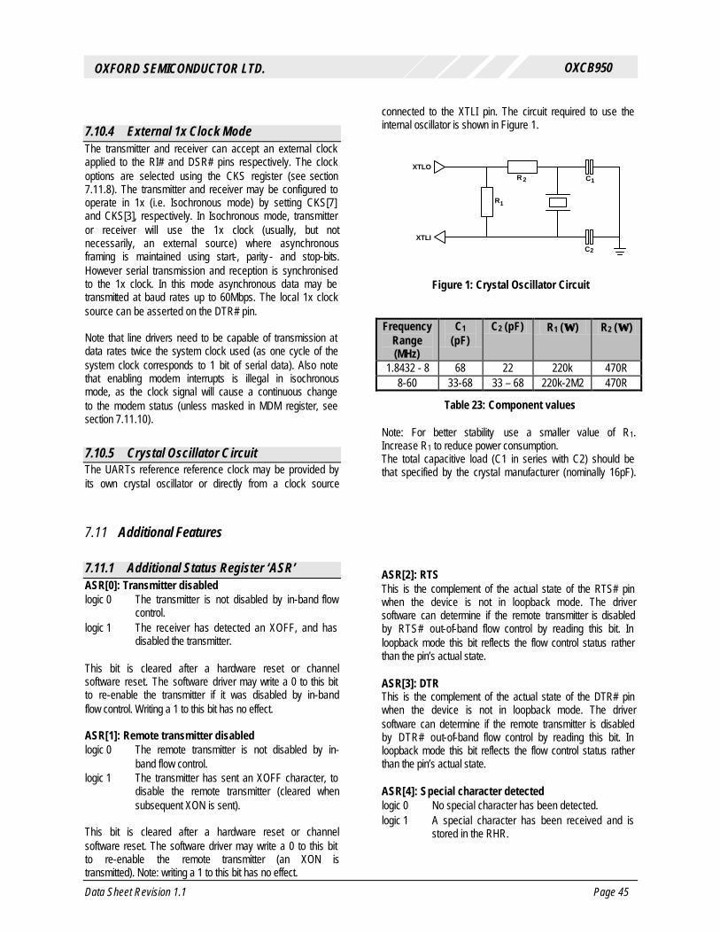
Data Sheet Revision 1.1 Page 45
OXCB950
OXFORD SEMICONDUCTOR LTD.
7.10.4 External 1x Clock Mode The transmitter and receiver can accept an external clock applied to the RI# and DSR# pins respectively. The clock options are selected using the CKS register (see section 7.11.8). The transmitter and receiver may be configured to operate in 1x (i.e. Isochronous mode) by setting CKS[7] and CKS[3], respectively. In Isochronous mode, transmitter or receiver will use the 1x clock (usually, but not necessarily, an external source) where asynchronous framing is maintained using start-, parity - and stop-bits. However serial transmission and reception is synchronised to the 1x clock. In this mode asynchronous data may be transmitted at baud rates up to 60Mbps. The local 1x clock source can be asserted on the DTR# pin. Note that line drivers need to be capable of transmission at data rates twice the system clock used (as one cycle of the system clock corresponds to 1 bit of serial data). Also note that enabling modem interrupts is illegal in isochronous mode, as the clock signal will cause a continuous change to the modem status (unless masked in MDM register, see section 7.11.10).
7.10.5 Crystal Oscillator Circuit The UARTs reference reference clock may be provided by its own crystal oscillator or directly from a clock source
connected to the XTLI pin. The circuit required to use the internal oscillator is shown in Figure 1.
R1
R 2 C1
C2
XTLI
XTLO
Figure 1: Crystal Oscillator Circuit Frequency
Range (MHz)
C1 (pF)
C2 (pF) R1 (ΩΩ ) R2 (ΩΩ )
1.8432 - 8 68 22 220k 470R 8-60 33-68 33 – 68 220k-2M2 470R
Table 23: Component values Note: For better stability use a smaller value of R1. Increase R1 to reduce power consumption. The total capacitive load (C1 in series with C2) should be that specified by the crystal manufacturer (nominally 16pF).
7.11 Additional Features
7.11.1 Additional Status Register ‘ASR’ ASR[0]: Transmitter disabled logic 0 ⇒ The transmitter is not disabled by in-band flow
control. logic 1 ⇒ The receiver has detected an XOFF, and has
disabled the transmitter. This bit is cleared after a hardware reset or channel software reset. The software driver may write a 0 to this bit to re-enable the transmitter if it was disabled by in-band flow control. Writing a 1 to this bit has no effect. ASR[1]: Remote transmitter disabled logic 0 ⇒ The remote transmitter is not disabled by in-
band flow control. logic 1 ⇒ The transmitter has sent an XOFF character, to
disable the remote transmitter (cleared when subsequent XON is sent).
This bit is cleared after a hardware reset or channel software reset. The software driver may write a 0 to this bit to re-enable the remote transmitter (an XON is transmitted). Note: writing a 1 to this bit has no effect.
ASR[2]: RTS This is the complement of the actual state of the RTS# pin when the device is not in loopback mode. The driver software can determine if the remote transmitter is disabled by RTS# out-of-band flow control by reading this bit. In loopback mode this bit reflects the flow control status rather than the pin’s actual state. ASR[3]: DTR This is the complement of the actual state of the DTR# pin when the device is not in loopback mode. The driver software can determine if the remote transmitter is disabled by DTR# out-of-band flow control by reading this bit. In loopback mode this bit reflects the flow control status rather than the pin’s actual state. ASR[4]: Special character detected logic 0 ⇒ No special character has been detected. logic 1 ⇒ A special character has been received and is
stored in the RHR.

Data Sheet Revision 1.1 Page 46
OXCB950
OXFORD SEMICONDUCTOR LTD.
This can be used to determine whether a level 5 interrupt was caused by receiving a special character rather than an XOFF. The flag is cleared following the read of the ASR. ASR[5]: FIFOSEL This bit reflects the unlatched state of the FIFOSEL pin. The OXCB950 returns ‘0’ for this bit as the FIFOSEL ‘pin’ is tied low internally. ASR[6]: FIFO size logic 0 ⇒ FIFOs are 16 deep if FCR[0] = 1. logic 1 ⇒ FIFOs are 128 deep if FCR[0] = 1. ASR[7]: Transmitter Idle logic 0 ⇒ Transmitter is transmitting. logic 1 ⇒ Transmitter is idle. This bit reflects the state of the internal transmitter. It is set when both the transmitter FIFO and shift register are empty.
7.11.2 FIFO Fill levels ‘TFL & RFL’ The number of characters stored in the THR and RHR can be determined by reading the TFL and RFL registers respectively. When data transfer is in constant operation, the values should be interpreted as follows: 1. The number of characters in the THR is no greater
than the value read back from TFL. 2. The number of characters in the RHR is no less than
the value read back from RFL.
7.11.3 Additional Control Register ‘ACR’ The ACR register is located at offset 0x00 of the ICR ACR[0]: Receiver disable logic 0 ⇒ The receiver is enabled, receiving data and
storing it in the RHR. logic 1 ⇒ The receiver is disabled. The receiver
continues to operate as normal to maintain the framing synchronisation with the receive data stream but received data is not stored into the RHR. In-band flow control characters continue to be detected and acted upon. Special characters will not be detected.
Changes to this bit will only be recognised following the completion of any data reception pending. ACR[1]: Transmitter disable logic 0 ⇒ The transmitter is enabled, transmitting any
data in the THR. logic 1 ⇒ The transmitter is disabled. Any data in the
THR is not transmitted but is held. However, in-band flow control characters may still be transmitted.
Changes to this bit will only be recognised following the completion of any data transmission pending.
ACR[2]: Enable automatic DSR flow control logic 0 ⇒ Normal. The state of the DSR# line does not
affect the flow control. logic 1 ⇒ Data transmission is prevented whenever the
DSR# pin is held inactive high. This bit provides another automatic out-of-band flow control facility using the DSR# line. ACR[4:3]: DTR# line configuration When bits 4 or 5 of CKS (offset 0x03 of ICR) are set, the transmitter 1x clock or the output of the baud rate generator (Nx clock) are asserted on the DTR# pin, otherwise the DTR# pin is defined as follows: logic [00] ⇒ DTR# is compatible with 16C450, 16C550,
16C650 and 16C750 (i.e. normal). logic [01] ⇒ DTR# pin is used for out-of-band flow control.
It will be forced inactive high if the Receiver FIFO Level (‘RFL’) reaches the upper flow control threshold. DTR# line will be re-activated (=0) when the RFL drops below the lower threshold (see FCL & FCH).
logic [10] ⇒ DTR# pin is configured to drive the active-low enable pin of an external RS485 buffer. In this configuration the DTR# pin will be forced low whenever the transmitter is not empty (LSR[6]=0), otherwise DTR# pin is high.
logic [11] ⇒ DTR# pin is configured to drive the active-high enable pin of an external RS485 buffer. In this configuration, the DTR# pin will be forced high whenever the transmitter is not empty (LSR[6]=0), otherwise DTR# pin is low.
If the user sets ACR[4], then the DTR# line is controlled by the status of the transmitter empty bit of LCR. When ACR[4] is set, ACR[3] is used to select active high or active low enable signals. In half-duplex systems using RS485 protocol, this facility enables the DTR# line to directly control the enable signal of external 3-state line driver buffers. When the transmitter is empty the DTR# would go inactive once the SOUT line returns to it’s idle marking state. ACR[5]: 950 mode trigger levels enable logic 0 ⇒ Interrupts and flow control trigger levels are as
described in FCR register and are compatible with 16C650/16C750 modes.
logic 1 ⇒ 950 specific enhanced interrupt and flow control trigger levels defined by RTL, TTL, FCL and FCH are enabled.
ACR[6]: ICR read enable logic 0 ⇒ The Line Status Register is readable. logic 1 ⇒ The Indexed Control Registers are readable.

Data Sheet Revision 1.1 Page 47
OXCB950
OXFORD SEMICONDUCTOR LTD.
Setting this bit will map the ICR set to the LSR location for reads. During normal operation this bit should be cleared. ACR[7]: Additional status enable logic 0 ⇒ Acces to the ASR, TFL and RFL registers is
disabled. logic 1 ⇒ Access to the ASR, TFL and RFL registers is
enabled. When ACR[7] is set, the MCR, LCR and IER registers are no longer readable but remain writable, and the registers ASR, TFL and RFL replace them in the register map for read operations. The software driver may leave this bit set during normal operation, since MCR, LCR and IER do not generally need to be read.
7.11.4 Transmitter Trigger Level ‘TTL’ The TTL register is located at offset 0x04 of the ICR Whenever 950 trigger levels are enabled (ACR[5]=1), bits 4 and 5 of FCR are ignored and an alternative arbitrary transmitter interrupt trigger level can be defined in the TTL register. This 7-bit value provides a fully programmable transmitter interrupt trigger facility. In 950 mode, a priority level 3 interrupt occurs indicating that the transmitter buffer requires more characters when the interrupt is not masked (IER[1]=1) and the transmitter FIFO level falls below the value stored in the TTL register. The value 0 (0x00) has a special meaning. In 950 mode when the user writes 0x00 to the TTL register, a level 3 interrupt only occurs when the FIFO and the transmitter shift register are both empty and the SOUT line is in the idle marking state. This feature is particularly useful to report back the empty state of the transmitter after its FIFO has been flushed away.
7.11.5 Receiver Interrupt. Trigger Level ‘RTL’ The RTL register is located at offset 0x05 of the ICR Whenever 950 trigger levels are enabled (ACR[5]=1), bits 6 and 7 of FCR are ignored and an alternative arbitrary receiver interrupt trigger level can be defined in the RTL register. This 7-bit value provides a fully programmable receiver interrupt trigger facility as opposed to the limited trigger levels available in 16C650 and 16C750 devices. It enables the system designer to optimise the interrupt performance hence minimising the interrupt overhead. In 950 mode, a priority level 2 interrupt occurs indicating that the receiver data is available when the interrupt is not masked (IER[0]=1) and the receiver FIFO level reaches the value stored in this register.
7.11.6 Flow Control Levels ‘FCL’ & ‘FCH’ The FCL and FCH registers are located at offsets 0x06 and 0x07 of the ICR respectively Enhanced software flow control using XON/XOFF and hardware flow control using RTS#/CTS# and DTR#/DSR# are available when 950 mode trigger levels are enabled (ACR[5]=1). Improved flow control threshold levels are offered using Flow Control Lower trigger level (‘FCL’) and Flow Control Higher trigger level (‘FCH’) registers to provide a greater degree of flexibility when optimising the flow control performance. Generally, these facilities are only available in Enhanced mode. In 650 mode, in-band flow control is enabled using the EFR register. An XOFF character may be transmitted when the receiver FIFO exceeds the upper trigger level defined by FCR[7:6] as described in section 7.4.1. An XON is then sent when the FIFO is read down the lower fill level. The flow control is enabled and the appropriate mode is selected using EFR[3:0]. In 950 mode, the flow control thresholds defined by FCR[7:6] are ignored. In this mode, threshold levels are programmed using FCL and FCH. When flow control is enabled by EFR[3:0] and the receiver FIFO level (‘RFL’) reaches the value programmed in the FCH register, one or two XOFFs may be transmitted to stop the flow of serial data as defined by EFR[3:0]. When the receiver FIFO level falls below the value programmed in FCL the flow is resumed by sending one or two XON characters (as defined in EFR[3:0]). The FCL value of 0x00 is illegal. CTS/RTS and DSR/DTR out-of-band flow control use the same trigger levels as in-band flow control. When out-of-band flow control is enabled, RTS# (or DTR#) line is de-asserted when the receiver FIFO level reaches the upper limit defined in the FCH and is re-asserted when the receiver FIFO is drained below a lower limit defined in FCL. When 950 trigger levels are enabled (ACR[5]=1), the CTS# flow control functions as in 650 mode and is configured by EFR[7]. However, RTS# is automatically de-asserted and re-asserted when EFR[6] is set and RFL reaches FCH and drops below FCL. DSR# flow control is configured with ACR[2]. DTR# flow control is configured with ACR[4:3].
7.11.7 Device Identification Registers The identification registers is located at offsets 0x08 to 0x0B of the ICR The UARTs offer four bytes of device identification. The device ID registers may be read using offset values 0x08 to 0x0B of the Indexed Control Register. Registers ID1, ID2 and ID3 identify the device as an OX16C950 and return 0x16, 0xC9 and 0x50 respectively. The REV register resides at offset 0x0B of ICR and identifies the revision of

Data Sheet Revision 1.1 Page 48
OXCB950
OXFORD SEMICONDUCTOR LTD.
950 core. This register returns 0x05 for revision A of the OX1CB950.
7.11.8 Clock Select Register ‘CKS’ The CKS register is located at offset 0x03 of the ICR This register is cleared to 0x00 after a hardware reset to maintain compatibility with 16C550, but is unaffected by software reset. This allows the user to select a clock source and then reset the channel to work-around any timing glitches. CKS[1:0]: Receiver Clock Source Selector logic [00] ⇒ The RCLK pin is selected for the receiver
clock (550 compatible mode). logic [01] ⇒ The DSR# pin is selected for the receiver
clock. logic [10] ⇒ The output of baud rate generator (internal
BDOUT#) is selected for the receiver clock. logic [11] ⇒ The transmitter clock is selected for the
receiver. This allows RI# to be used for both transmitter and receiver.
CKS[2]: Reserved CKS[3]: Receiver 1x clock mode selector logic 0 ⇒ The receiver is in Nx clock mode as defined in
the TCR register. After a hardware reset the receiver operates in 16x clock mode, i.e. 16C550 compatibility.
logic 1 ⇒ The receiver is in isochronous 1x clock mode. CKS[5:4]: Transmitter 1x clock or baud rate generator output (BDOUT) on DTR# pin logic [00] ⇒ The function of the DTR# pin is defined by
the setting of ACR[4:3]. logic [01] ⇒ The transmitter 1x clock (bit rate clock) is
asserted on the DTR# pin and the setting of ACR[4:3] is ignored.
logic [10] ⇒ The output of baud rate generator (Nx clock) is asserted on the DTR# pin and the setting of ACR[4:3] is ignored.
logic [11] ⇒ Reserved. CKS[6]: Transmitter clock source selector logic 0 ⇒ The transmitter clock source is the output of the
baud rate generator (550 compatibility). logic 1 ⇒ The transmitter uses an external clock applied
to the RI# pin. CKS[7]: Transmitter 1x clock mode selector logic 0 ⇒ The transmitter is in Nx clock mode as defined
in the TCR register. After a hardware reset the transmitter operates in 16x clock mode, i.e. 16C550 compatibility.
logic 1 ⇒ The transmitter is in isochronous 1x clock mode.
7.11.9 Nine-bit Mode Register ‘NMR’ The NMR register is located at offset 0x0D of the ICR The UART offers 9-bit data framing for industrial multi-drop applications. The 9-bit mode is enabled by setting bit 0 of the Nine-bit Mode Register (NMR). In 9-bit mode the data length setting in LCR[1:0] is ignored. Furthermore as parity is permanently disabled, the setting of LCR[5:3] is also ignored. The receiver stores the 9th bit of the received data in LSR[2] (where parity error is stored in normal mode). Note that the UART provides a 128-deep FIFO for LSR[3:0]. The transmitter FIFO is 9 bits wide and 128 deep. The user should write the 9th (MSB) data bit in SPR[0] first and then write the other 8 bits to THR. As parity mode is disabled, LSR[7] is set whenever there is an overrun, framing error or received break condition. It is unaffected by the contents of LSR[2] (Now the received 9th data bit). In 9-bit mode, in-band flow control is disabled regardless of the setting of EFR[3:0] and the XON1/XON2/XOFF1 and XOFF2 registers are used for special character detection. Interrupts in 9-Bit Mode: While IER[2] is set, upon receiving a character with status error, a level 1 interrupt is asserted when the character and the associated status are transferred to the FIFO. The UART can assert an optional interrupt if a received character has its 9th bit set. As multi-drop systems often use the 9th bit as an address bit, the receiver is able to generate an interrupt upon receiving an address character. This feature is enabled by setting NMR[2]. This will result in a level 1 interrupt being asserted when the address character is transferred to the receiver FIFO. In this case, as long as there are no errors pending, i.e. LSR[1], LSR[3], and LSR[4] are clear, '0' can be read back from LSR[7] and LSR[1], thus differentiating between an ‘address’ interrupt and receiver error or overrun interrupt in 9-bit mode. Note however that should an overrun or error interrupt actually occur, an address character may also reside in the FIFO. In this case, the software driver should examine the contents of the receiver FIFO as well as process the error. The above facility produces an interrupt for recognizing any ‘address’ characters. Alternatively, the user can configure the UART to compare the receiver data stream with up to four programmable 9-bit characters and assert a level 5 interrupt after detecting a match. The interrupt occurs when the character is transferred to the FIFO (See below).
Data Sheet Revision 1.1 Page 49
OXCB950
OXFORD SEMICONDUCTOR LTD.
NMR[0]: 9-bit mode enable logic 0 ⇒ 9-bit mode is disabled. logic 1 ⇒ 9-bit mode is enabled. NMR[1]: Enable interrupt when 9th bit is set logic 0 ⇒ Receiver interrupt for detection of an ‘address’
character (i.e. 9th bit set) is disabled. logic 1 ⇒ Receiver interrupt for detection of an ‘address’
character (i.e. 9th bit set) is enabled and a level 1 interrupt is asserted.
Special Character Detection While the UART is in both 9-bit mode and Enhanced mode, setting IER[5] will enable detection of up to four ‘address’ characters. The least significant eight bits of these four programmable characters are stored in special characters 1 to 4 (XON1, XON2, XOFF1 and XOFF2 in 650 mode) registers and the 9th bit of these characters are programmed in NMR[5] to NMR[2] respectively. NMR[2]: Bit 9 of Special Character 1 NMR[3]: Bit 9 of Special Character 2 NMR[4]: Bit 9 of Special Character 3 NMR[5]: Bit 9 of Special Character 4 NMR[7:6]: Reserved Bits 6 and 7 of NMR are always cleared and reserved for future use.
7.11.10 Modem Disable Mask ‘MDM’ The MDM register is located at offset 0x0E of the ICR This register is cleared after a hardware reset to maintain compatibility with 16C550. It allows the user to mask interrupts, sleep operation and power management events due to individual modem lines or the serial input line. MDM[0]: Disable delta CTS logic 0 ⇒ Delta CTS is enabled. It can generate a level 4
interrupt when enabled by IER[3]. In power-state D2, delta CTS can assert the PME# line. Delta CTS can wake up the UART when it is asleep under auto-sleep operation.
logic 1 ⇒ Delta CTS is disabled. In can not generate an interrupt, assert a PME# or wake up the UART.
MDM[1]: Disable delta DSR logic 0 ⇒ Delta DSR is enabled. It can generate a level 4
interrupt when enabled by IER[3]. In power-state D2, delta DSR can assert the PME# line. Delta DSR can wake up the UART when it is asleep under auto-sleep operation.
logic 1 ⇒ Delta DSR is disabled. In can not generate an interrupt, assert a PME# or wake up the UART.
MDM[2]: Disable Trailing edge RI
logic 0 ⇒ Trailing edge RI is enabled. It can generate a level 4 interrupt when enabled by IER[3]. In power-state D2, trailing edge RI can assert the PME# line. Trailing edge RI can wake up the UART when it is asleep under auto-sleep operation.
logic 1 ⇒ Trailing edge RI is disabled. In can not generate an interrupt, assert a PME# or wake up the UART.
MDM[3]: Disable delta DCD logic 0 ⇒ Delta DCD is enabled. It can generate a level 4
interrupt when enabled by IER[3]. In power-state D2, delta DCD can assert the PME# line. Delta DCD can wake up the UART when it is asleep under auto-sleep operation.
logic 1 ⇒ Delta DCD is disabled. In can not generate an interrupt, assert a PME# or wake up the UART.
MDM[4]: Reserved This bit must be set to ‘0’ MDM[5]: Disable SIN wake up logic 0 ⇒ When the device is in power-down state D2, a
change in the state of the serial input line (i.e. start bit) can assert the PME# line
logic 1 ⇒ When the device is in power-down state D2, a change in the state of the serial input line cannot assert the PME# line.
MDM[7:6]: Reserved
7.11.11 Readable FCR ‘RFC’ The RFC register is located at offset 0x0F of the ICR This read-only register returns the current state of the FCR register (Note that FCR is write-only). This register is included for diagnostic purposes.
7.11.12 Good-data status register ‘GDS’ The GDS register is located at offset 0x10 of the ICR For the definition of Good-data status refer to section Error! Reference source not found.. GDS[0]: Good Data Status GDS[7:1]: Reserved
Data Sheet Revision 1.1 Page 50
OXCB950
OXFORD SEMICONDUCTOR LTD.
7.11.13 DMA Status Register ‘DMS’ The DMS register is located at offset 0x11 of the ICR. This allows the internal TXRDY# and RXRDY# lines to be permanently deasserted, and the current internal status to be monitored. This mainly has applications for testing. DMS[0]: RxRdy Status Read Only: set when RxRdy is asserted (pin driven low). DMS[1]: TxRdy Status Read Only: set when TxRdy is asserted (pin driven low). DMS[5:2] Reserved DMS[6]: Force RxRdy Inactive logic 0 ⇒ RxRdy# acts normally logic 1 ⇒ RxRdy# is permanently inactive (high)
regardless of FIFO thresholds DMA[7]: Force TxRdy Inactive logic 0 ⇒ TxRdy# acts normally logic 1 ⇒ TxRdy# is permanently inactive (high)
regardless of FIFO thresholds.
7.11.14 Port Index Register ‘PIX’ The PIX register is located at offset 0x12 of the ICR. This read-only register gives the UART index. For a single channel device such as the OX16C950 this reads ‘0’.
7.11.15 Clock Alteration Register ‘CKA’ The CKA register is located at offset 0x13 of the ICR. This register adds additional clock control mainly for isochronous and embedded applications. The register is effectively an enhancement to the CKS register. This register is cleared to 0x00 after a hardware reset to maintain compatibility with 16C550, but is unaffected by software reset. This allows the user to select a clock mode and then reset the channel to work-around any timing glitches.

Data Sheet Revision 1.1 Page 51
OXCB950
OXFORD SEMICONDUCTOR LTD.
8 SERIAL EEPROM SPECIFICATION
The OXCB950 can be configured using an optional serial electrically-erasable programmable read only memory (EEPROM). If the EEPROM is not present, the device will remain in its default configuration after reset. Although this may be adequate for some applications, many will benefit from the degree of programmability afforded by this feature. The EEPROM also allows accesses to the integrated UART, which can be useful for default setups. The EEPROM interface supports a variety of serial EEPROM devices that have a proprietary serial interface known as MicrowireTM. This interface has four pins which supply the memory device with a clock, a chip-select, and serial data input and output lines. In order to read from such a device, a controller has to output serially a read command and address, then input serially the data. The interface controller has been designed to handle (autodetect) the following list of compatible devices that have a 16-bit data word format but differ in memory size (and hence the number of address bits). NM93C46 (64 WORDS), NM93C56 (128 WORDS), devices with 256 WORDS, 512 WORDs and 1024 WORDS. The OXCB950 incorporates a controller module which reads data from the serial EEPROM and writes data into the relevant register space. It performs this operation in a sequence which starts immediately after a cardbus/PCI bus reset and ends either when the controller finds no EEPROM is present or when it reaches the end of the eeprom data. Note that any attempted cardbus/PCI access while the eeprom is being sensed or data is being downloaded from the serial EEPROM will result in a “retry” response. The operation of this controller is described below. Following device configuration, driver software can access the serial EEPROM through four bits in the device-specific Local Configuration Register LCC[27:24]. Software can use this register to manipulate the device pins in order to read and modify the EEPROM contents as desired. A Windows based utility to program the EEPROM is available. For further details please contact Oxford Semiconductor (see back cover). MicrowireTM is a trade mark of National Semiconductor. For a description of MicrowireTM, please refer to National Semiconductor data manuals.
8.1 EEPROM Data Organisation
The serial EEPROM data is divided into six zones. The size of each zone is an exact multiple of 16-bit WORDs. Zone0 is allocated to the header. An EEPROM program must contain a valid header before any further data is interrogated. The EEPROM can be programmed from the PCI bus. Once the programming is complete, the device driver should either reset the PCI bus or set LCC[29] to reload the OXCB950 registers from the serial EEPROM. The general EEPROM data structure is shown in Table 24.
DATA Zone
Size (Words)
Description
0 One Header 1 One or more Power (Management) Data 2 One to more Local Configuration Registers 3 Two or more Cardbus Information Structure 4 Two or more PCI Configuration Registers 5 Multiples of 2 Function Access
Table 24: EEPROM data format
8.1.1 Zone0: Header The header identifies the EEPROM program as valid.
Bits Description 15:8 These bits should return 0xB5 to identify a valid
program. Once the OXCB950 reads 0xB5 from these bits, it sets LCC[28] to indicate that a valid EEPROM program is present.
7:5 Reserved for future Zones. Set to 0. 4 1 = Zone1 (Power Management Data) exists
0 = Zone1 does not exist 3 1 = Zone2 (Local Configuration) exists
0 = Zone2 does not exist 2 1 = Zone3 (Cardbus Information structure) exists
0 = Zone3 does not exist 1 1 = Zone4 (PCI Configuration) exists
0 = Zone4 does not exist 0 1 = Zone5 (Function Access) exists
0 = Zone5 does not exist The programming data for each zone follows the proceeding zone if it exists. For example a Header value of 0xB51F indicates that all zones exist and they follow one another in sequence (from Zone1 to Zone5), while 0xB514 indicates that only Zones 1 and 3 exist where the header data is followed by Zone1 WORDs, and since Zone2 is missing Zone1 WORDs are followed by Zone3 WORDs.
Data Sheet Revision 1.1 Page 52
OXCB950
OXFORD SEMICONDUCTOR LTD.
8.1.2 Zone1 : Power Management DATA, DATA_SCALE zone Zone 1 region of the EEPROM provides the power management registers with user values for the DATA and DATA_SCALE fields, that will be provided to the system software when requests are made through the DATA_SELECT field.
Since there are 16 possible values for the DATA_SELECT fields, the system can request up to 16 sets of DATA and DATA_SCALE values. The organisation of the EEPROM data for this zone is shown in the table. Each DATA and DATA_SCALE value being programmed is relevant to a particular value of the DATA_SELECT parameter.
Bits Description 15 ‘0’ = There are no more Configuration WORDs
to follow in Zone1. Move to the next available zone or end EEPROM program if no more zones are enabled in the Header. ‘1’ = There is another Configuration WORD to follow for the Power Management Data zone.
14 Reserved. To be written as ‘0’ 13:10 DATA SELECT
This indicates for which DATA_SELECT value the DATA and DATA_SCALE values in this particular word are associated with.
9:8 DATA SCALE Value For the Data Select Field in this word
7:0 DATA Register Value For the Data Select Field in this word.
Data Sheet Revision 1.1 Page 53
OXCB950
OXFORD SEMICONDUCTOR LTD.
8.1.3 Zone2: Local Configuration Register Zone The Zone2 region of EEPROM contains the program value of the vendor-specific Local Configuration Registers using one or more configuration WORDs. Registers are selected using a 7-bit byte-offset field. This offset value is the offset from Base Address Registers in I/O or memory space (see section 6.4). Note: Not all of the registers in the Local Configuration Register set are
writable by EEPROM. The format of configuration WORDs for the Local Configuration Registers in Zone1 are described in Table 25.
Bits Description 15 ‘0’ = There are no more Configuration WORDs
to follow in Zone2. Move to the next available zone or end EEPROM program if no more zones are enabled in the Header. ‘1’ = There is another Configuration WORD to follow for the Local Configuration Registers.
14:8 These seven bits define the byte-offset of the Local configuration register to be programmed. For example the byte-offset for LCC[23:16] is 0x02.
7:0 8-bit value of the register to be programmed
Table 25: Zone 2 data format
8.1.4 Zone 3 : Cardbus Information Structure This zone allows the user to provide custom tuple information for the Cardbus Information Structure, overriding the default hardcoded tuple values found in the device. Downloading into this zone programs an internal RAM with the user’s tuple data and automatically sets the source of the cardbus information structure to be this RAM. This process sets the local configuration register bit LCC(21) to 1. The format of the EEPROM organisation for this zone is shown by the table. The first word indicates the number of
tuple data bytes to follow (in multiples of 2 NOTE1) and the subsequent words contain the actual tuple data-bytes to be inserted into the cardbus information structure that will be visible at Dword18 or 32 in the PCI configuration space. Tuple data bytes are interrogated until the specified number of tuple data-bytes have been collected in which case the EEPROM moves over to the next zone if it exists, or the eeprom download terminates if no other zones are present.
Description 1st WORD NO of TUPLE bytes to follow, in binary.
This sets a counter that will terminate download into this zone when the correct number of Tuple Bytes have been collected. (Value to be in multiples of 2 NOTE1)
2nd WORD Tuple Byte 1 Tuple Byte 0 3th WORD Tuple Byte 3 Tuple Byte 2 nth WORD Tuple Byte y+1 Tuple Byte y
NOTE1 If the number of tuple bytes to be programmed into RAM is an odd number, it will be necessary to add a NULL tuple to make the total
number of tuple bytes to be a multiple of 2. The data in the cardbus information structure is organised according to the order in which the tuple data has been collected. This is as shown
CIS : Tuple Byte3, Tuple Byte 2, Tuple Byte 1, Tuple Byte 0 Tuple Byte7, Tuple Byte 6, Tuple Byte 5, Tuple Byte 4

Data Sheet Revision 1.1 Page 54
OXCB950
OXFORD SEMICONDUCTOR LTD.
8.1.5 Zone4: PCI Configuration Registers The Zone4 region of EEPROM contains any changes required to the PCI Configuration registers (including the Vendor ID and Subsystem Vendor ID). This zone consists of a function header WORD, and one or more configuration WORDs for that function. The function header is described in Table 26.
Bits Description 15 ‘0’ = End of Zone 4.
‘1’ = Define this function header. 14:3 Reserved. Write zeros. 2:0 Function number for the following configuration
WORD(s). ‘000’ = Function0 Other values = Reserved.
Table 26: Zone 4 data format (Function Header) The subsequent WORDs for each function contain the address offset and a byte of programming data for the PCI Configuration Space belonging to the function number selected by the proceeding Function-Header. The format of configuration WORDs for the PCI Configuration Registers are described below.
Bits Description 15 ‘0’ = This is the last configuration WORD in for
the selected function in the Function-Header. ‘1’ = There is another WORD to follow for this function.
14:8 These seven bits define the byte-offset of the PCI configuration register to be programmed. For example the byte-offset of the Interrupt Pin register is 0x3D. Offset values are tabulated in section 6.2.
7:0 8-bit value of the register to be programmed
Table 27: Zone 4 data format (data) Table 28 shows which PCI Configuration registers are writable from the EEPROM.
Offset Bits Description 0x00 7:0 Vendor ID bits 7 to 0. 0x01 7:0 Vendor ID bits 15 to 8. 0x02 7:0 Device ID bits 7 to 0. 0x03 7:0 Device ID bits 15 to 8. 0x06 3:0 Must be ‘0000’. 0x06 4 Extended Capabilities. 0x06 7:5 Must be ‘000’. 0x09 7:0 Class Code bits 7 to 0. 0x0A 7:0 Class Code bits 15 to 8. 0x0B 7:0 Class Code bits 23 to 16. 0x2C 7:0 SubsystemVendor ID bits 7 to 0. 0x2D 7:0 SubsystemVendor ID bits 15 to 8. 0x2E 7:0 Subsystem ID bits 7 to 0. 0x2F 7:0 Subsystem ID bits 15 to 8. 0x3D 7:0 Interrupt pin. 0x42 7:0 Power Management Capabilities
bits 7 to 0. 0x43 7:0 Power Management Capabilities
bits 15 to 8.
Table 28: EEPROM-writable PCI configuration registers

Data Sheet Revision 1.1 Page 55
OXCB950
OXFORD SEMICONDUCTOR LTD.
8.1.6 Zone5: Function Access Zone 5 allows the UART to be pre-configured, prior to any cardbus/PCI accesses. This is very useful when the UART needs to run with (typically generic) device drivers and these drivers are not capable of utilising the enhanced features/modes of the UART (eg 950 mode) that are required for high performance. By using function access, the UART registers can be accessed (setup) via the eeprom to customize the UART features before control is handed to the device drivers.
Each 8-bit (function) access is equivalent to accessing the UART function through I/O BAR 0, with the exception that a function read access does not return any data (it is discarded). The UART function behaves as though these function accesses via the eeprom were corresponding cardbus/pci accesses. Each entry for zone 5 comprises 2 16 bit words. The format is as shown in Table 14.
1st WORD of FUNCTION ACCESS PAIR
Word Bits Description 15 ‘1’ - another WORD to follow 14:12 BAR number to access
000 for BAR 0 (UART IO BAR) Others values are reserved
11 ‘0’ : Read access required(data will be discarded) ‘1’ : Write access required
10:8 Reserved – write 0’s 7:0 I/O address to access
This is the address that needs to be written/read and is the offset address from the specified BAR. E.g to access SPR register of UART, address is 00000111 (7dec).
2nd WORD of FUNCTION ACCESS PAIR
Word Bits Description 15 ‘1’ – another function access WORD pair to follow.
‘0’ – no more function access word pairs. End EEPROM program.
14:8 Reserved – write 0’s 7:0 Data to be written to specified address.
Field is unused for function access READS (set to 0’s for reads)

Data Sheet Revision 1.1 Page 56
OXCB950
OXFORD SEMICONDUCTOR LTD.
Function Access Examples 1) Enable Internal loopback (Enable bit 4, MCR register)
1000100000000100 BAR No = 000 (UART), Write Access, Address=00000100 (MCR reg)
1000000000010000 Data to be written=00010000 (bit4) 2) Enable FIFO (Enable bit 0, FCR register)
1000100000000010 BAR No = 000 (UART), Write access, address=00000010 (FCR reg) 1000000000000001 Data to be written=00000001 (bit 1) 3) Read IER Register
1000000000000001 BAR No =000 (UART), Read access, address=00000001 (IER reg) 1000000000000000 No data to be written (as read access). Read data is discarded.

Data Sheet Revision 1.0 PRELIMINARY Page 57
OXCB950 OXFORD SEMICONDUCTOR LTD.
9 COMPLIANCE TO PC CARD STANDARDS, 7.0 AND 7.1
This section is relevant only to the cardbus application of the OXCB950. The OXCB950 requires the presence of the PCI_CLK for reliable operation of the internal UART. Since the presence of the pci clk is governed by the cardbus connector signal CCLKRUN#, this connector pin must be kept asserted to ensure the pci_clk is not stopped, for full functionality. The OXCB950 is, however, tolerant to fluctuations in the pci clk line. The cheapest option to maintain the pci_clk is to hold the CCLKRUN# pin asserted through the use of a 1K0
pulldown resistor. This is compatible with PC Card Standards 7.0, and all PC Card Standards prior to the release of version 7.1. PC Card Standard 7.1, however, does not allow the use of this pulldown for new designs and all new designs that are not tolerant to the clock stopping are required to implement the clock run protocol on the CCLKRUN# line. The clock run protocol can be implemented externally through the use of the following circuitry and allows the OXCB950 part to be compliant to version 7.1 of the PC Card Standard.
The circuitry to implement the clock control logic on the CCLKRUN# signal line is a synchronous 2-bit shift register (implemented via 2 D-type FF's) that utilises the logic signal appearing on the CCLKRUN# line as DATA, as well as driving the CCLKRUN# line through an open-collector transistor. This arrangement creates a controlled loop from the CCLKRUN# pin, through the logic, and back onto the CCLKRUN# pin. The circuitry is enabled or disabled
through the use of the oxcb950's multi-purpose IO pin, MIO0, that is controlled by Oxford Semiconductor's custom device-driver for the oxcb950 device. When the oxcb950, with this modification, is inserted into the PC cardbus slot then the clock control circuitry is disabled by virtue of the pulldown connected on the MIO0 pin. This is because the state of the MIO0 pin following a
D Q CLR
74LV74 (so)
D QCLR
74LV74 (so)
MIO0
CCLK
CCLKRUN#

Data Sheet Revision 1.0 PRELIMINARY Page 58
OXCB950 OXFORD SEMICONDUCTOR LTD.
reset is hi-impedance. As the circuitry is disabled, the transistor connected to the CCLKRUN# line is off and so the state of the CCLKRUN# signal pin is controlled by the host, which will be holding the pin in the asserted state (clock running) as the inserted device needs to be enumerated and configured. When the operating system hands control to the custom device driver, the device driver will assigned a logic '1' to the pin MIO0 to enable the clock control circuitry which will begin to monitor the status of the CCLKRUN# line. While the host continues to assert the CCLKRUN# line, to indicate clock run, the clock control circuitry continuously samples logic '0' that results in the open-collector transistor being held in the off-state.
When the host intends on stopping the clock, it negates the CCLKRUN# line by synchronously driving the CCLKRUN# line to logic '1' and then releasing its drive to this line. This will also result in the CCLKRUN# line being a logic '1' due to the presence of a pull-up on the host end of the interface. When the clock control circuitry has sampled the negation of the CCLKRUN# line for 2 samples, this results in the open-collector transistor to be driven, thereby asserting the CCLKRUN# line (this time by the target). In other words, the clock control circuitry asserts the CCLKRUN# line 2 clocks after it had been negated by the host. This is the required signalling to the host to prevent it from completing its original intention of stopping the clock. The clock line CCLK continues to run uninterrupted.
CCLK
Q1
Q2/ transistor drive
CCLKRUN#
CLKRUN# driven by host. Clock control circuitry contains all 0’s thus keeping transistor off
Host synchronously negates CCLKRUN# to indicate intention of stopping clock.
Clock control samples CCLKRUN# negated for 1 clock cycle
Clock control samples CCLKRUN# negated for 2 clock cycles. Turns on transistor to assert CCLKRUN# line.
Clock control negates drive to transistor, but CCLKRUN# now held asserted by the host (during period transistor was driven)
CCLK continues to run Uninterrupted.
Data Sheet Revision 1.0 PRELIMINARY Page 59
OXCB950 OXFORD SEMICONDUCTOR LTD.
Now that the target has signalled that the clock is to be maintained, the target's drive on the CCLKRUN# line must be maintained for 2 clocks during which the host will begin to drive the line also. Since the CCLKRUN# is also the data to the 2-bit shift register then, when the CCLKRUN# is driven by the control circuitry, it will take 2 clock cycles for the new clock run status to propagate through the logic to turn off the transistor. During this period, the host will have detected the assertion of the CCLKRUN# by the target and will also begin to assert the CLKRUN# line, so that when the clock control's transistor is turned off, the CCLKRUN# will be held in the asserted state by the host thereby keeping the transistor off. The transistor will remain off until the host next attempts to negate the CCLKRUN# line to indicate a clock stop and is prevented from doing so by the clock control logic. For the condition when the device driver needs to place the oxcb950 into a low powerstate, and the clock control logic
is not required, then the device driver will assign the MIO0 pin to a logic 0 that disables the clock control circuitry and forces the clockrun transistor to the off state. For this condition, when the host negates the CCLKRUN# line it does not see the CCLKRUN# being asserted by the target (as the circuitry has been disabled) and the clock is stopped by the host after the relevant number of clocks from the negation. Since the UART functionality within the oxcb950 device is not dependant upon the CCLK line for interrupt generation, then any activity within the UART that results in an interrupt will be conveyed to the cardbus interface asynchronously. This will result in the CCLKRUN# being asserted by the host (and thus enabling the clock CCLK) and control will be handed to the device driver that will re-enable the clock control circuitry to prevent the clock from stopping until all tasks have been completed.
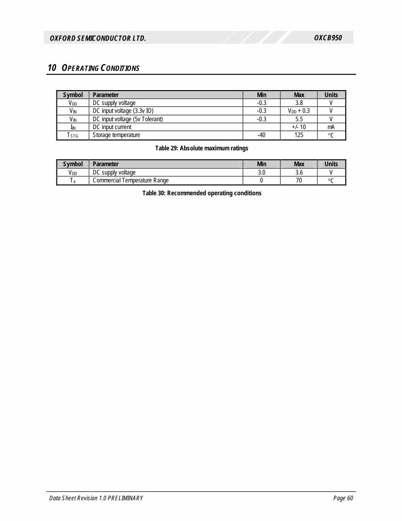
Data Sheet Revision 1.0 PRELIMINARY Page 60
OXCB950 OXFORD SEMICONDUCTOR LTD.
10 OPERATING CONDITIONS
Symbol Parameter Min Max Units
VDD DC supply voltage -0.3 3.8 V VIN DC input voltage (3.3v IO) -0.3 VDD + 0.3 V VIN DC input voltage (5v Tolerant) -0.3 5.5 V IIN DC input current +/- 10 mA
TSTG Storage temperature -40 125 °C
Table 29: Absolute maximum ratings
Symbol Parameter Min Max Units VDD DC supply voltage 3.0 3.6 V Ta Commercial Temperature Range 0 70 °C
Table 30: Recommended operating conditions

Data Sheet Revision 1.0 PRELIMINARY Page 61
OXCB950 OXFORD SEMICONDUCTOR LTD.
11 DC ELECTRICAL CHARACTERISTICS
11.1 Normal 3.3v I/O Buffers
Vdd = 3.3v +/- 0.3v, Ta = 0 to 70c
Symbol Parameter Condition Min Max Units VIH High level input voltage LVCMOS Interface 1
LVCMOS Schmitt trig 1 2.0 2.0
V
VIL Low level input voltage LVCMOS Interface 1 LVCMOS Schmitt trig 1
0.8 0.8
V
CIN Cap of input buffers See Note 2 4.0 pF COUT Cap of output buffers See Note 2 4.0 pF
IIH High level input current Vin = VDD, no pull-ups. -10 10 µA IIL Low level input current Vin = VSS, no pull-ups -10 10 µA
VOH High level output voltage IOH = -1 µA VDD – 0.05 V VOH High level output voltage IOH = -1mA to -12mA 2.4 V VOL Low level output voltage IOL = 1 µA 0.05 V VOL Low level output voltage IOL = 1mA to 12 mA 0.4 V IOZ Tri-state output leakage current Vout = Vss or Vdd -10 10 µA
Table 31: Characteristics of Normal I/O buffers
Note 1: LVCMOS is compatible with TTL levels at 3.3v Note 2: This value excludes package parasitics
11.2 5.0v Tolerant I/O Buffers
Vdd = 3.3v +/- 0.3v, Vext = 5.0v +/- 0.25v, Ta = 0 to 70c
Symbol Parameter Condition Min Max Units VIH 2 High level input voltage LVCMOS Interface 1
LVCMOS Schmitt trig 1 2.0 2.0
V
VIL 2 Low level input voltage LVCMOS Interface 1
LVCMOS Schmitt trig 1 0.8
0.8 V
CIN Cap of input buffers See Note 3 4.0 pF COUT Cap of output buffers See Note 3 4.0 pF
IIH High level input current Vin = VDD, no pull-ups. -10 10 µA IIL Low level input current Vin = VSS, no pull-ups -10 10 µA
VOH High level output voltage IOH = -1 µA VDD – 0.05 V VOH High level output voltage IOH = -1mA to -6mA 2.4 V VOL Low level output voltage IOL = 1 µA 0.05 V VOL Low level output voltage IOL = 1mA to 6 mA 0.4 V IOZ Tri-state output leakage current Vout = Vss or Vext -10 10 µA
Table 32: Characteristics of 5v tolerant I /O buffers
Note 1: LVCMOS is compatible with TTL levels at 3.3v Note 2: All 5v tolerant inputs have less than 0.2v hysteresis
Note 3: This value excludes package parasitics
Data Sheet Revision 1.0 PRELIMINARY Page 62
OXCB950 OXFORD SEMICONDUCTOR LTD.
11.3 Dual Mode (Cardbus/PCI) I/O Buffers
PCI Mode (ENCB=’0’) The Dual Mode I/O buffers are compliant to the DC and AC Electrical Characteristics of the 3.3v signalling environment, as defined in the PCI Local Bus Specification, revision 2.2. (Sections 4.2.2.1 and 4.2.2.2 of this specification) Cardbus Mode (ENCB=’1’) The Dual Mode I/O buffers are compliant to the DC and AC Electrical Characteristics for 3.3v signalling, as defined in the PC Card Standard, release 7.x. (Sections 5.3.2.1.1 and 5.3.2.1.2 of this specification).

Data Sheet Revision 1.0 PRELIMINARY Page 63
OXCB950 OXFORD SEMICONDUCTOR LTD.
12 POWER CONSUMPTION MEASUREMENTS
The following values are actual current measurements for the oxcb950 device using prototype test boards. These values are to be treated as indicators and do not necessarily represent actual figures or incur statistical spreads associated with production parts.
12.1 Static current consumption
• DC current with the PCI clock and XTLI pins grounded 100uA • Current drawn with the XTL1 Pin grounded but with the PCI interface clock running. 7.8mA
12.2 Current consumption in application
• Current when no accesses have been made to the UART and the UART automatically enters its sleep state. 4.5mA
• Current when the UART is in full operation, transmitting and receiving via internal
loopback at maximum data rate (DLLDLM=1). 14mA • Current when the UART divisor latch has been set to maximum divide and the UART
is in full speed operation. 12mA • Current when the (UART) power management state is configured to power states D2 3.2mA
• Current when the (UART) power management state is configured to power states D3 3.2mA

Data Sheet Revision 1.0 PRELIMINARY Page 64
OXCB950 OXFORD SEMICONDUCTOR LTD.
13 Timing Waveforms
CLK
FRAME#
AD[31:0]
C/BE[3:0]#
IRDY#
TRDY#
DEVSEL#
STOP#
Address
Bus CMD Byte enable#
1 2 3 4
Data
Dat
a tra
nsfe
r
Figure 1: PCI Read transaction from the PCI Configuration Space (Reads of Cardbus CIS tuples –also in pci configuration space- incurs an additional pci clock cycle)
CLK
FRAME#
AD[31:0]
C/BE[3:0]#
IRDY#
TRDY#
DEVSEL#
STOP#
Address
Bus CMD Byte enable#
1 2 3 4
Data
Dat
a tra
nsfe
r
Figure 2: PCI Write transaction to the PCI Configuration Space (Writes to the Cardbus CIS tuples – also in the pci configuration space - incur 2 additional pci clk cycles)
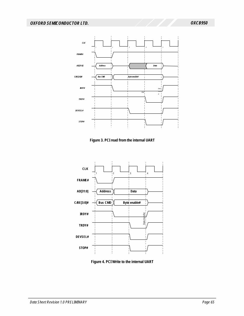
Data Sheet Revision 1.0 PRELIMINARY Page 65
OXCB950 OXFORD SEMICONDUCTOR LTD.
CLK
FRAME#
AD[31:0]
C/BE[3:0]#
IRDY#
TRDY#
DEVSEL#
STOP#
Address
Bus CMD Byte enable#
1 2 3 4 5
Data
Wait
Data
transf
er
Figure 3. PCI read from the internal UART
CLK
FRAME#
AD[31:0]
C/BE[3:0]#
IRDY#
TRDY#
DEVSEL#
STOP#
Address
Bus CMD Byte enable#
1 2 3 4
Data
Dat
a tra
nsfe
r
Figure 4. PCI Write to the internal UART
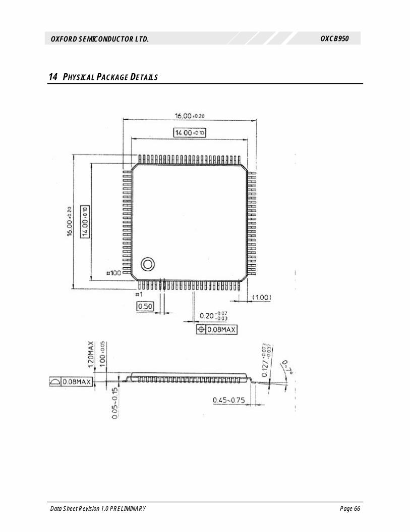
Data Sheet Revision 1.0 PRELIMINARY Page 66
OXCB950 OXFORD SEMICONDUCTOR LTD.
14 PHYSICAL PACKAGE DETAILS

Data Sheet Revision 1.0 PRELIMINARY Page 67
OXCB950 OXFORD SEMICONDUCTOR LTD.
This page has been intentionally left blank
Data Sheet Revision 1.0 PRELIMINARY Page 68
OXCB950 OXFORD SEMICONDUCTOR LTD.
CONTACT DETAILS
Oxford Semiconductor Ltd. 25 ParkGate Milton Park Abingdon Oxfordshire OX14 4SH United Kingdom Telephone: +44 (0)1235 824900 Fax: +44 (0)1235 821141 Sales e-mail: [email protected] Web site: http://www.oxsemi.com
DISCLAIMER
Oxford Semiconductor believes the information contained in this document to be accurate and reliable. However, it is subject to change without notice. No responsibility is assumed by Oxford Semiconductor for its use, nor for infringement of patents or other rights of third parties. No part of this publication may be reproduced, or transmitted in any form or by any means without the prior consent of Oxford Semiconductor Ltd. Oxford Semiconductor’s terms and conditions of sale apply at all times.


![[PPT]UART and UART Driver - University at Buffalobina/cse321/fall2009/UARTDriver.ppt · Web viewUART and UART Driver B. Ramamurthy * UART UART: Universal Asynchronous Receiver/Transmitter](https://img.dokumen.tips/doc/110x75/5b2ab3637f8b9a55068b752f/pptuart-and-uart-driver-university-at-binacse321fall2009uartdriverppt.jpg)