Embed Size (px)
Citation preview

1 1 TEM Samples preparation_D.Laub_2014
2 2
OVERVIEW OF SAMPLE PREPARATION TECHNIQUES FOR TRANSMISSION ELECTRON MICROSCOPY IN MATERIALS SCIENCE
TEM Samples preparation_D.Laub_2014
Why is the specimen preparation so important ?
Because no good sample preparation, no good TEM observation !!!

3 3
Ion Milling
Ultramicrotomy
Why is the sample preparation so important ? Because no good sample preparation, no good TEM observation !!!
Mica sample (mineral)
TEM Samples preparation_D.Laub_2014
4 4
Cross section, zone axis [0001], Ion Milling (>2kV) Cross section, zone axis [0001] , Ion Milling
(down to 100V)
Why is the sample preparation so important ?
TEM Samples preparation_D.Laub_2014

5 5
INTRODUCTION Size and thickness of the sample Diameter: 3 mm 1) Reduce size of large sample 2) Use 3 mm grid support for small sample
Thickness: between 10 et 200 nm depending on the material and the kind of observation to be done
1) depend on chemical composition 2) high resolution observation, EELS analysis or not
3 mm diameter
TEM Samples preparation_D.Laub_2014
6 6 !
INTRODUCTION !!!
Electrons transparent area, yes, but how, where ???
Hole!
Edge!
Edge!
Full thin lamella
TEM Samples preparation_D.Laub_2014

7 7
INTRODUCTION
Sample has to be: ♣ electrically conductive
♣ stable under vacum
♣ free of hydrocarbures contamination
♣ should not contain artefacts that could lead to a
wrong analyse The sample for TEM observation must be representative of
the true nature and morphology of the material
It would be impossible to prepare a sample without any artefact, so the best method has to be choosen depending on the type of analyse needed and the type of artefacts
induced by one or the other technique
TEM Samples preparation_D.Laub_2014
8 8
Metal!Semiconducteor!Ceramics!Mineral!Biological!Polymer!Composite!
Sample orientation !
-Any!
-Particular!!
How to choose the preparation technique in relation with the material and the analysis to be done
Choice of technique depending on analysis
to be done and/or induced artefact!
Material! Geometry!
Small size materials: fibers, nanotubes, …!
Bulk!
Multilayer!
Physical !structure!
Compact!
Porous!
Liquid phase!
Chemical !phases!
Monophased!
Multiphased!
Physical !properties!
Hard!
Soft!
Fragile!
Resistant!
Analysis!
Technique adaption depending on
material !
Electrical!properties!
Conductive!
Insulating!
Ductile!
INTRODUCTION
TEM Samples preparation_D.Laub_2014

9 9
Mechanical-physical
INTRODUCTION
Mechanical + ionic
DIFFERENT TYPES OF PREPARATIONS: • Mechanical polishing down to electron transparency • Cleavage • Ultramicrotomy • Crushing • Nanoparticles dispersion
• Grinding, (dimpling), ion milling • FIB
• Electro-chemical polishing • Chemical polishing or etching
• Replica (direct or double) • Thin film deposition • …
Mechanical
Chemical
Physical
Ionic
TEM Samples preparation_D.Laub_2014
10 10
TECHNIQUES Dispersing Electron transparent Nanoparticles for TEM
Observation: random direction
Observations: • Particles size and shape • HRTEM • Diffraction • EDX analysis • …
TEM Samples preparation_D.Laub_2014

11 11
Working with nanoparticles or nanofibers Safety rule n° 1: preparation under fume hood !
Absolutely not needed Not needed but up to you ! Absolutely needed
Safety glasses Better nytrile gloves
TEM Samples preparation_D.Laub_2014
12 12
Choice of solvent to disperse particles
Ethanol: polar Toluene: non polar
Polar, non polar or does not matter ?
TEM Samples preparation_D.Laub_2014
Polar solvents have large dipole moments (aka “partial charges”); they contain bonds between atoms with very different electronegativities, such as oxygen - hydrogen.
Non polar solvents have low dielectric constants (<5) and are not good solvents for charged species such as anions.

13 13
Dispersion
Concentration
Ultrasound
Dilution
Ready to pick up the droplet
TEM Samples preparation_D.Laub_2014
Dispersion time needed: from 1 minute to several hours
Ultrasonic Device to Disperse Nanomaterial
14 14
One droplet on the grid: 3 ways
Dry under infra-red or standard desk lamp
With the perfect loop Dispersion
TEM Samples preparation_D.Laub_2014

15 15
" Standard carbon coated grid (C thickness 25–40 nm) 1 " Ultrathin carbon film (4–5 nm) 2 " Holey carbon film with ultrathin carbon windows (5 nm) " Holey carbon film 3 " Lacey carbon film 4 " …
Depends on the analysis to be done and the particles size
Selection of suitable support grid
1
2 3
4
TEM Samples preparation_D.Laub_2014
16 16
A few examples of dispersion
SiO2_Fe particles
C nanotubes
Before TEM observation
At least 1 hour under infra-red or standard desk lamp = removal of some hydrocarbons
Au particles
TEM Samples preparation_D.Laub_2014
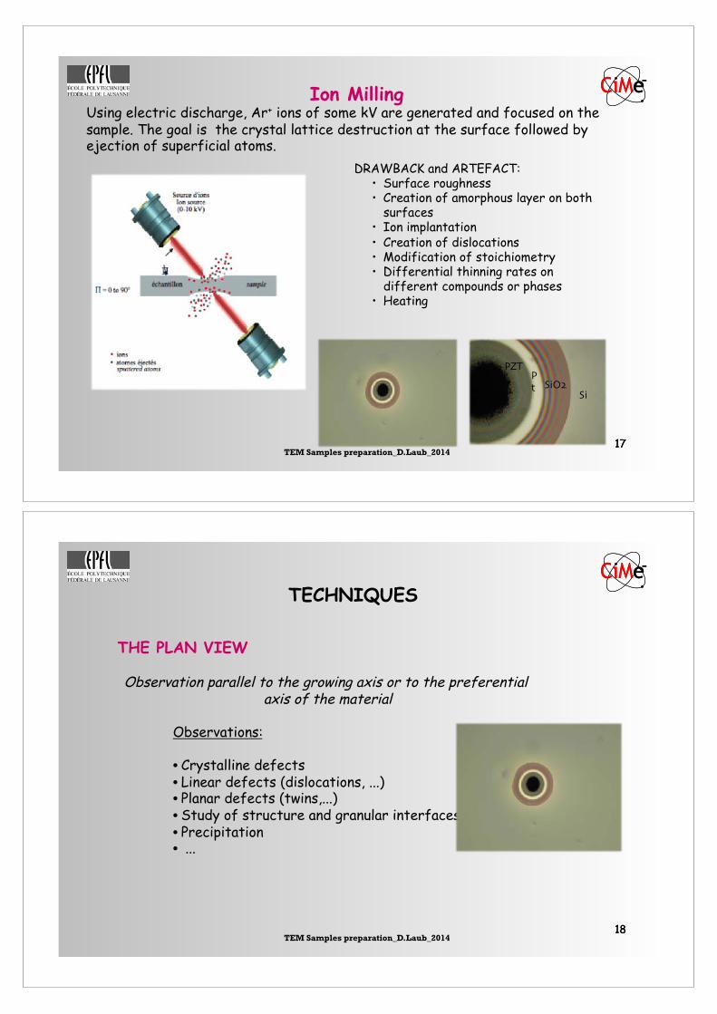
17 17
Ion Milling Using electric discharge, Ar+ ions of some kV are generated and focused on the sample. The goal is the crystal lattice destruction at the surface followed by ejection of superficial atoms.
DRAWBACK and ARTEFACT: • Surface roughness • Creation of amorphous layer on both
surfaces • Ion implantation • Creation of dislocations • Modification of stoichiometry • Differential thinning rates on
different compounds or phases • Heating
PZT!Pt! SiO2!
Si!
TEM Samples preparation_D.Laub_2014
18 18
TECHNIQUES THE PLAN VIEW Observation parallel to the growing axis or to the preferential
axis of the material
Observations: • Crystalline defects • Linear defects (dislocations, ...) • Planar defects (twins,...) • Study of structure and granular interfaces • Precipitation • ...
TEM Samples preparation_D.Laub_2014

19 19
# Super conducting wire Preparation : wedge mechanical polishing + ion milling 20 min
Sample + TEM observation : N.Merck
Planar view of a supra-conducting wire TEM image, bright field!
Advantage: large thin area Drawback: no information about different positions along the observation axis
SrTiO3 Grains boundary (J.Ayache)
TEM Samples preparation_D.Laub_2014
20 20
Materials: -All kind Method:
Possible defects • Dislocations • Irradiation • Amorphisation of surface layers • Modification of chemical composition
TEM Samples preparation_D.Laub_2014

21 21
Observation perpendicular to the growing axis or to the preferential axis of the material
Advantage: observation of anisotropy along the growing axis Drawback: small thin area Observations: • characterization of multilayer materials
• -layers thickness measurement
• -layers and interfaces structure analysis
CROSS-SECTION
e-!
TEM Samples preparation_D.Laub_2014
22 22
!!!
Method!
e
e

23 23
TiO2 / Silicon, Optical microscope, reflected light!
THE TRIPOD METHOD Mechanical thinning, in a wedge configuration, down to electron transparency
or to a thickness that requires very short ion milling time
TiO2/Si Planar view
D ir ec ti on o f m o ti on
Area of interest
TEM Samples preparation_D.Laub_2014
24 24
The Tripod tool
TEM Samples preparation_D.Laub_2014

25 25
Preparation for the first side polishing!
L part
Glass
TEM Samples preparation_D.Laub_2014
Sample
Polishing with diamond-impregnated lapping films; Finish with colloidal silica
26 26
Second side polishing
Polishing from back side
Area of interest
TEM Samples preparation_D.Laub_2014

27 27
Result after final polishing for a Si substrate sample
Si3N4/ Si optical microscope, transmitted light
TiO2/ Si, optical microscope, reflected light
TEM Samples preparation_D.Laub_2014
28 28
• 4 areas to observe • Easy to manipulate • Needs longer ion milling time
Planar polishing using Tripod polisher
TEM Samples preparation_D.Laub_2014

29 29
Same sample after ion milling: 1h at 5 keV, 10 min at 2 keV, 16° angle, 2 guns.
Experimental conditions
After final polishing. The arrow shows the glue line.
SOME EXAMPLES
Example 1: InP/GaAs cross -section
InP/GaAs interface:TEM, bright field
Image L. Sagalowicz, EPFL.
TEM Samples preparation_D.Laub_2014
30 30
GaN on sapphire substrate
Additional ion milling: 15 minute, 3 and 2kV, 2 guns, sectorial rotation, 5° angle
TEM image, dark field TEM image, bright field
TEM Samples preparation_D.Laub_2014

31 31
Thin PbLaTiO3 ferroelectric film on SrTiO3 substrate
Tripod no ion milling
Dimpler+ions
TEM observation
J. Ayache, CSNSM-CNRS-IN2P3, 91405 Orsay TEM Samples preparation_D.Laub_2014
32 32
THE FOCUSED ION BEAM (FIB) METHOD
Gaz: usually Galium
TEM Samples preparation_D.Laub_2014

33 33
For: - Planar view - cross-section - any orientation
F.Bobard, M. Cantoni
The FIB ( Focused Ion Beam )
Beams Coincidence Point
H-Bar method
TEM Samples preparation_D.Laub_2014
34 34
The FIB ( Focused Ion Beam )
Preparation of lamella H-bar method
FIB prép.: F.Bobard Images MET: M. Cantoni, CIME-EPFL
Nb3Sn multifilaments /bronze matrix!
TEM Samples preparation_D.Laub_2014
35 35
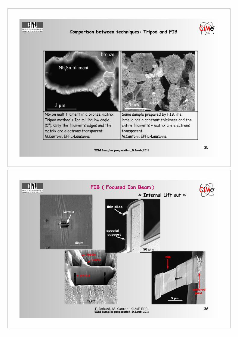
Nb3Sn multifilament in a bronze matrix.Tripod method + Ion milling low angle(5°). Only the filaments edges and thematrix are electrons transparentM.Cantoni, EPFL-Lausanne
Same sample prepared by FIB.Thelamella has a constant thickness and theentire filaments + matrix are electronstransparentM.Cantoni, EPFL-Lausanne
Comparison between techniques: Tripod and FIB
TEM Samples preparation_D.Laub_2014
36 36
!
FIB ( Focused Ion Beam )!« Internal Lift out »!
!!!
F. Bobard, M. Cantoni, CIME-EPFL!TEM Samples preparation_D.Laub_2014

37 37
THE CLEAVED WEDGE METHOD The cleaved wedge is a monocrystalline substrate (+ layers), dimension about 0.6/0.6 mm, obtained by 2 or 3 cleavages along designed atomic planes that give a perfect edge. Cleavage: make use of the fact that crystals may be split along planes which are weakly bonded
GaAs wafer e.g
TEM Samples preparation_D.Laub_2014
38 38
Origin of the contrast: • The observed contrast is linked to the sample thickness and
its chemical composition • As for a cleaved wedge, the sample thickness is accurately
known, the chemical composition can be deduced from the thickness fringes profile
• The electron beam is parallel to the layer interfaces • The layer interfaces are put forward by a discontinuity
of the fringes (perpendicularly to the wedge edge)
P.A. Buffat, J.D. Ganière, EPFL.
e- beam
TEM Samples preparation_D.Laub_2014
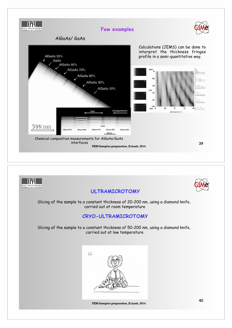
39 39 Chemical composition measurements for AlGaAs/GaAs
interfaces
Calculations (JEMS) can be done to interpret the thickness fringes profile in a semi-quantitative way.
AlGaAs/ GaAs
Few examples
TEM Samples preparation_D.Laub_2014
40 40
ULTRAMICROTOMY
Slicing of the sample to a constant thickness of 20-200 nm, using a diamond knife, carried out at room temperature
CRYO-ULTRAMICROTOMY
Slicing of the sample to a constant thickness of 50-200 nm, using a diamond knife,
carried out at low temperature
TEM Samples preparation_D.Laub_2014

41 41
ULTRAMICROTOMY, CRYO-ULTRAMICROTOMY
Observations • Statistic of particles size • EDX chemical analysis, EELS chemical analysis (needs thin constant thickness) • Material microstructure • Cross-section or plan view of materials that cannot be ion milled, mechanically or electrolytically thinned
• Heterogeneous materials, multilayer • Small diameter fibres or tips • Powders (metallic or not)
Materials • Polymer /polymers with additional compounds • Catalyst • Geological • Biomaterial • Wood • Metal
Drawback: • Deformation of the sample due to compression or/and cracks • Dislocations • Shape modification • …
TEM Samples preparation_D.Laub_2014
42 42
The ultramicrotome The knives
PS spheres in Epon cuted with a 15° knife cut with a 45° knife
Courtesy Helmut Gnaegi, Diatome
• Cutting speed control • Thickness selection
TEM Samples preparation_D.Laub_2014

43 43
&!
• Reduce the sample size if needed!!• Embed the sample if needed!
Method!
Particles! Multilayer! Bulk!
Important: the embedding resin should have the same hardness/ softness as the sample
For porous material: embedding under vacuum or infiltration-embedding
TEM Samples preparation_D.Laub_2014
44 44 TEM Samples preparation_D.Laub_2014

45 45 TEM Samples preparation_D.Laub_2014
46 46
• Section thickness 40 - 50nm • Sectioning speed 0.2mm/sec
Cutting the sample to the desired (or possible) thickness
Diatome, Helmut Gnaegi presentation
Damage induced
TEM Samples preparation_D.Laub_2014

47 47
Section collection – “fishing”!
Diatome, Helmut Gnaegi presentation TEM Samples preparation_D.Laub_2014
48 48
Results
TEM, bright field image Optical microscope, transmited light
Diatome, Helmut Gnaegi presentation TEM Samples preparation_D.Laub_2014

49 49
Drawback
Tin sample TEM bright field image
Higher magnification Carbon particles in epoxy resin TEM, bright field image J.Ayache, UMR-CNRS-IGR, Villejuif
Si-Fe/SiO2 particles Embedded in epoxy TEM bright field image
TEM Samples preparation_D.Laub_2014
50 50
ELECTRO-CHEMICAL POLISHING (JET POLISHING)
Effect of electrolytical polishing is due to anodic dissolution of a pre-polished surface in an electrolyte bath
• A bath for the electrolyte • A continuous current source • An anode (the sample) • A cathode
Observations: • Dislocations
(orientation)
• Twins (macles)
• Grain boundaries
• precipitates and phases
• ….
Infra-red detector
Pump
Sample holder
Infra-red receptor
Electrolyte
Counter-electrode
Nose Sample
TEM Samples preparation_D.Laub_2014

51 51
Aiming for the plateau
TEM Samples preparation_D.Laub_2014
Use highly acidic electropolishing solutions (e.g. 70% phosphoric acid for water) => – metal surface cannot passivate (no oxide layer) – metal highly soluble, dissolves at high rate Solution has high viscosity, therefore metal ions cannot diffuse quickly – metal precipitates into salt (Jacquet layer) Rate of dissolution controlled by diffusion of metal ions from surface; Dissolution faster at peaks than troughs => polishing regime in which sample becomes flatter as it etches
52 52
Material must be an electrical conductor
• Metal and alloys, one or more phases• Carbides• Graphite• Some oxides• Some composite materials with metallic matrix and fine
particles
Ni3Al matrix with Mo fibres, TEM dark field image
Advantage: non destructive method
Drawback: may cause preferential etching, dissolution of interface or some phases Possible damages: eventually residual oxidation layer at the sample surface
TEM Samples preparation_D.Laub_2014

53 53
• Observations: • Similar to the plan-view or cross-section
• Materials: • Metals • Semiconductors • oxides • glass • ...
Method: • Cutting and/or cross section procedure • Polishing onto soft tissue, specific for chemical addition • Chemical thinning until hole
CHEMICAL POLISHING
Same principle as electro-polishing but more difficult to control The solutions are more reactive and used at higher temperature
Advantage: possible for non conductive materials Drawback: dislocations, etching (etch pits)
Possible damages: residual oxidation layer at the sample surface
TEM Samples preparation_D.Laub_2014
54 54
THE REPLICA METHOD The replica is the reproduction of the sample surface topography. It is done by polymer, carbone or oxide film deposition onto the surface sample, which is then removed from the sample and observed intoTEM.
Observations • Multiphase materials • Surface topography • Second phase particles analysis obtained by the extraction replica method • Radiation sensitive samples
Method • Film deposition, either « soft » polymer or in a solvant solution • Carbon film deposition for non conductive samples
• Pulling away the film from the sample by its immersion into solvant, by pulling out or by chemical etching of the sample. • Mounting the replica onto a 2.3 mm or 3 mm support grid
TEM Samples preparation_D.Laub_2014

55 55
!!!
Direct replica!Indirect replica
Extractive replica Sample
Sample
Pt;Au;W Metal shadowing
Carbon coating
Sample
Carbon
inverted topography
Sample
Sample
Polymer
Metal shadowing
Pt;Au;W
Polymer
Polymer
Carbon
Particles Particles in relief Polished face
Carbon
(a) (b)
(c) (d)
Matrix dissolution Carbon coating
Etching
Non-inverted topography
TEM Samples preparation_D.Laub_2014
56 56 TEM Samples preparation_D.Laub_2014


![Chapter 2 Sample preparation, and others1 Chapter 2 Sample preparation, and others [Summary of sample preparation method] Sample preparation is highly important to perform analytical](https://img.dokumen.tips/doc/110x75/5e9216dec3c2053e873640d8/chapter-2-sample-preparation-and-1-chapter-2-sample-preparation-and-others-summary.jpg)