Embed Size (px)
Citation preview

December 2007 Rev 6 1/17
17
TS971-TS972-TS974
Output rail-to-rail very low noise operational amplifier
Features■ Rail-to-rail output voltage swing
±2.4V @ VCC = ±2.5V
■ Very low noise level: 4nV/√Hz
■ Ultra low distortion: 0.003%
■ High dynamic features: 12MHz, 4V/µs
■ Operating range: 2.7V to 10V
■ ESD protection (2kV)
■ Latch-up immunity (class A)
Applications■ Portable equipment (CD players, PDA)
■ Portable communications (cell phones, pagers)
■ Instrumentation & sensoring
■ Professional audio circuits
DescriptionThe TS97x family of operational amplifiers operates with voltages as low as ±1.35V and features output rail-to-rail signal swing. The TS97x are particularly well suited for portable and battery-supplied equipment. Very low noise and low distortion characteristics make them ideal for audio pre-amplification.
The TS971 is available in a variety of packages to suit all types of applications. For applications where space-saving is critical, the SOT23 package (2.8 x 2.9mm) or the DFN package (3 x 3mm) simplify the board design because they can be placed everywhere.
TS971ILT (SOT23-5L)
�
�
� �
�
���� ��� �������� ��� ��� ����
������
���
���
TS971ID-TS971IDT (SO-8)
�
�
�
� �
�
�
�
�
�
���� ����������
����
���� ��� ����������
���
���
��������
����
����
�
�
�
� �
�
�
�
�
� �
�
���� ����������
��������
���� ��� ����������
���
���
��������
���� ����������
���� ��� ����������
TS972IN (DIP8)TS972ID-TS972IDT (SO-8)
TS972IPT (TSSOP8)
TS972IQT (DFN8)
1
2
3
4 5
6
7
8Output 1
Inverting Input 1
Non Inverting Input 1
VDD
VCC
Output 2
Inverting Input 2
Non Inverting Input 2
1
2
3
4 5
6
7
8Output 1
Inverting Input 1
Non Inverting Input 1
VDD
VCC
Output 2
Inverting Input 2
Non Inverting Input 2
TS974IN (DIP14)TS974ID-TS974IDT (SO-14)
TS974IPT (TSSOP14)
���� ����������
���� ��� ����������
���� ��� ����������
���
�
�
�
�
�
�
�
�
�
��
��
��
��
��
��������
��������
��������
���� ��� ����������
���� ����������
���� ��� ����������
���� ����������
�
�
�
�
�
�
�
�
��������
���� ����������
��������
www.st.com

Absolute maximum ratings and operating conditions TS971-TS972-TS974
2/17
1 Absolute maximum ratings and operating conditions
Table 1. Absolute maximum ratings AMR
Symbol Parameter Value Unit
VCC Supply voltage (1)
1. All voltage values, except differential voltage are with respect to network ground terminal.
12 V
Vid Differential input voltage (2)
2. Differential voltages are the non-inverting input terminal with respect to the inverting input terminal.
±1 V
Vin Input voltage (3)
3. The magnitude of input and output voltages must never exceed VCC +0.3V.
VDD -0.3 to VCC
+0.3 V
Tstg Storage temperature range -65 to +150
Tj Maximum junction temperature 150 °C
Rthja
Thermal resistance junction to ambient (4)
SOT23-5DFN8SO-8SO-14TSSOP8TSSOP14DIP8DIP14
4. Short-circuits can cause excessive heating and destructive dissipation. Values are typical.
25040
1251051201008580
°C/W
Rthjc
Thermal resistance junction to case(4)
SOT23-5DFN8SO-8SO-14TSSOP8TSSOP14DIP8DIP14
815.2403137324133
°C/W
ESD
HBM: human body model(5)
5. Human body model: A 100pF capacitor is charged to the specified voltage, then discharged through a 1.5kΩ resistor between two pins of the device. This is done for all couples of connected pin combinations while the other pins are floating.
2 kV
MM: machine model(6)
6. Machine model: A 200pF capacitor is charged to the specified voltage, then discharged directly between two pins of the device with no external series resistor (internal resistor < 5Ω). This is done for all couples of connected pin combinations while the other pins are floating.
200 V
CDM: charged device model(7)
7. Charged device model: all pins and the package are charged together to the specified voltage and then discharged directly to the ground through only one pin. This is done for all pins.
No value specified for CDM on SOT23-5 package.
1.5 kV
Lead temperature (soldering, 10sec) 260 °C

TS971-TS972-TS974 Absolute maximum ratings and operating conditions
3/17
Table 2. Operating conditions
Symbol Parameter Value Unit
VCC Supply voltage 2.7 to 10 V
Vicm Common mode input voltage range VDD +1.15 to VCC -1.15 V
Toper Operating free air temperature range -40 to +125 °C
Electrical characteristics TS971-TS972-TS974
4/17
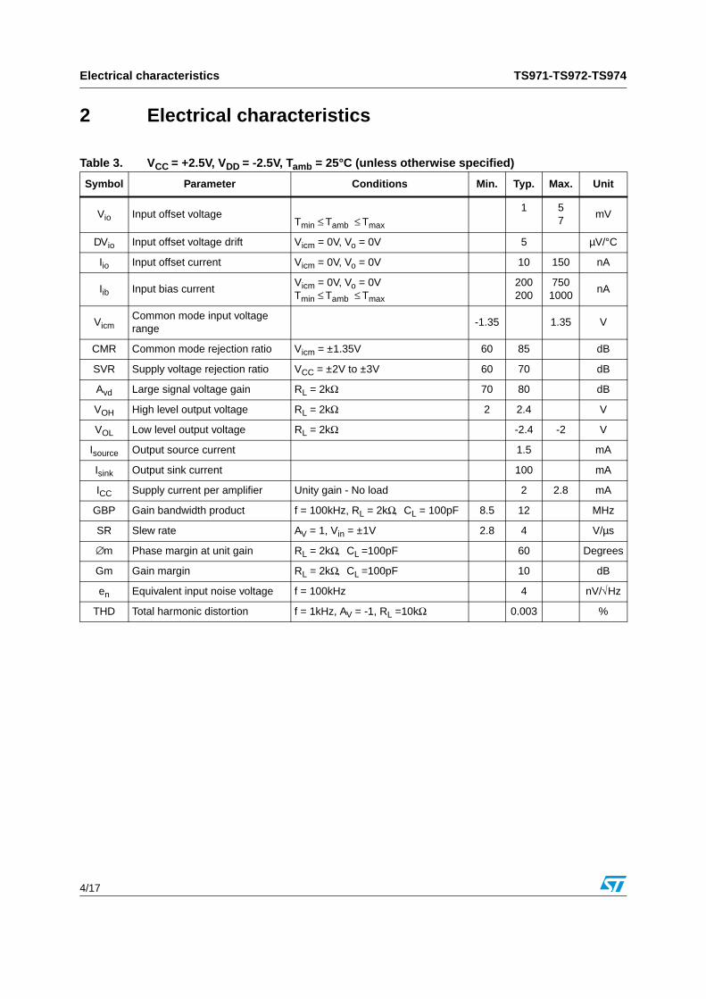
2 Electrical characteristics
Table 3. VCC = +2.5V, VDD
= -2.5V, Tamb = 25°C (unless otherwise specified)
Symbol Parameter Conditions Min. Typ. Max. Unit
Vio Input offset voltageTmin ≤ Tamb ≤ Tmax
1 57
mV
DVio Input offset voltage drift Vicm = 0V, Vo = 0V 5 µV/°C
Iio Input offset current Vicm = 0V, Vo = 0V 10 150 nA
Iib Input bias current Vicm = 0V, Vo = 0VTmin ≤ Tamb ≤ Tmax
200200
7501000
nA
VicmCommon mode input voltage range
-1.35 1.35 V
CMR Common mode rejection ratio Vicm = ±1.35V 60 85 dB
SVR Supply voltage rejection ratio VCC = ±2V to ±3V 60 70 dB
Avd Large signal voltage gain RL = 2kΩ 70 80 dB
VOH High level output voltage RL = 2kΩ 2 2.4 V
VOL Low level output voltage RL = 2kΩ -2.4 -2 V
Isource Output source current 1.5 mA
Isink Output sink current 100 mA
ICC Supply current per amplifier Unity gain - No load 2 2.8 mA
GBP Gain bandwidth product f = 100kHz, RL = 2kΩ, CL = 100pF 8.5 12 MHz
SR Slew rate AV = 1, Vin = ±1V 2.8 4 V/µs
∅m Phase margin at unit gain RL = 2kΩ, CL =100pF 60 Degrees
Gm Gain margin RL = 2kΩ, CL =100pF 10 dB
en Equivalent input noise voltage f = 100kHz 4 nV/√Hz
THD Total harmonic distortion f = 1kHz, AV = -1, RL =10kΩ 0.003 %

TS971-TS972-TS974 Electrical characteristics
5/17
Figure 1. Input offset voltage distribution Figure 2. Voltage gain & phase vs. frequency
Figure 3. Voltage gain & phase vs. frequency Figure 4. THS vs. Vout
Figure 5. THD vs. Vout Figure 6. THD vs. frequency

Electrical characteristics TS971-TS972-TS974
6/17
Figure 7. Noise voltage vs. frequency Figure 8. Gain bandwidth product vs. Iout
Figure 9. Phase margin vs. Iout Figure 10. Phase margin vs. VCC
Figure 11. Phase margin vs. VCC Figure 12. Gain margin vs. VCC

TS971-TS972-TS974 Package information
7/17
3 Package information
In order to meet environmental requirements, ST offers these devices in ECOPACK® packages. These packages have a lead-free second level interconnect. The category of second level interconnect is marked on the package and on the inner box label, in compliance with JEDEC Standard JESD97. The maximum ratings related to soldering conditions are also marked on the inner box label. ECOPACK is an ST trademark. ECOPACK specifications are available at: www.st.com.
3.1 SOT23-5 package information
Figure 13. SOT23-5 package mechanical drawing
Table 4. SOT23-5 package mechanical data
Ref.Millimeters Mils
Min. Typ. Max. Min. Typ. Max.
A 0.90 1.45 35.4 57.1
A1 0.00 0.15 0.00 5.9
A2 0.90 1.30 35.4 51.2
b 0.35 0.50 13.7 19.7
C 0.09 0.20 3.5 7.8
D 2.80 3.00 110.2 118.1
E 2.60 3.00 102.3 118.1
E1 1.50 1.75 59.0 68.8
e 0.95 37.4
e1 1.9 74.8
L 0.35 0.55 13.7 21.6

Package information TS971-TS972-TS974
8/17
3.2 DIP8 package information
Figure 14. DIP8 package mechanical drawing
Table 5. DIP8 package mechanical data
Ref.
Dimensions
Millimeters Inches
Min. Typ. Max. Min. Typ. Max.
A 5.33 0.210
A1 0.38 0.015
A2 2.92 3.30 4.95 0.115 0.130 0.195
b 0.36 0.46 0.56 0.014 0.018 0.022
b2 1.14 1.52 1.78 0.045 0.060 0.070
c 0.20 0.25 0.36 0.008 0.010 0.014
D 9.02 9.27 10.16 0.355 0.365 0.400
E 7.62 7.87 8.26 0.300 0.310 0.325
E1 6.10 6.35 7.11 0.240 0.250 0.280
e 2.54 0.100
eA 7.62 0.300
eB 10.92 0.430
L 2.92 3.30 3.81 0.115 0.130 0.150

TS971-TS972-TS974 Package information
9/17
3.3 SO-8 package information
Figure 15. SO-8 package mechanical drawing
Table 6. SO-8 package mechanical data
Ref.
Dimensions
Millimeters Inches
Min. Typ. Max. Min. Typ. Max.
A 1.75 0.069
A1 0.10 0.25 0.004 0.010
A2 1.25 0.049
b 0.28 0.48 0.011 0.019
c 0.17 0.23 0.007 0.010
D 4.80 4.90 5.00 0.189 0.193 0.197
H 5.80 6.00 6.20 0.228 0.236 0.244
E1 3.80 3.90 4.00 0.150 0.154 0.157
e 1.27 0.050
h 0.25 0.50 0.010 0.020
L 0.40 1.27 0.016 0.050
k 1° 8° 1° 8°
ccc 0.10 0.004

Package information TS971-TS972-TS974
10/17
3.4 TSSOP8 package information
Figure 16. TSSOP8 package mechanical drawing
Table 7. TSSOP8 package mechanical data
Ref.
Dimensions
Millimeters Inches
Min. Typ. Max. Min. Typ. Max.
A 1.2 0.047
A1 0.05 0.15 0.002 0.006
A2 0.80 1.00 1.05 0.031 0.039 0.041
b 0.19 0.30 0.007 0.012
c 0.09 0.20 0.004 0.008
D 2.90 3.00 3.10 0.114 0.118 0.122
E 6.20 6.40 6.60 0.244 0.252 0.260
E1 4.30 4.40 4.50 0.169 0.173 0.177
e 0.65 0.0256
k 0° 8° 0° 8°
L 0.45 0.60 0.75 0.018 0.024 0.030
L1 1 0.039
aaa 0.1 0.004

TS971-TS972-TS974 Package information
11/17
3.5 DIP14 package information
Figure 17. DIP14 package mechanical drawing
Table 8. DIP14 package mechanical data
Ref.
Dimensions
Millimeters Inches
Min. Typ. Max. Min. Typ. Max.
a1 0.51 0.020
B 1.39 1.65 0.055 0.065
b 0.5 0.020
b1 0.25 0.010
D 20 0.787
E 8.5 0.335
e 2.54 0.100
e3 15.24 0.600
F 7.1 0.280
I 5.1 0.201
L 3.3 0.130
Z 1.27 2.54 0.050 0.100
Package information TS971-TS972-TS974
12/17
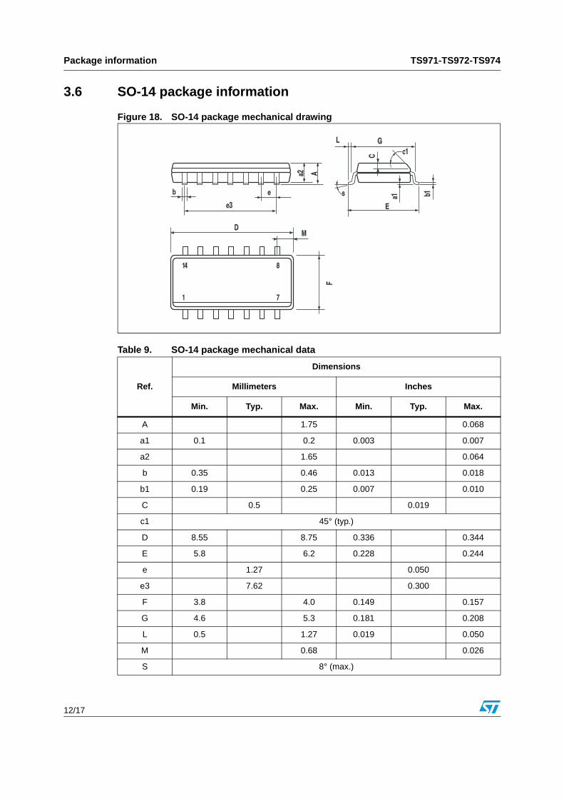
3.6 SO-14 package information
Figure 18. SO-14 package mechanical drawing
Table 9. SO-14 package mechanical data
Ref.
Dimensions
Millimeters Inches
Min. Typ. Max. Min. Typ. Max.
A 1.75 0.068
a1 0.1 0.2 0.003 0.007
a2 1.65 0.064
b 0.35 0.46 0.013 0.018
b1 0.19 0.25 0.007 0.010
C 0.5 0.019
c1 45° (typ.)
D 8.55 8.75 0.336 0.344
E 5.8 6.2 0.228 0.244
e 1.27 0.050
e3 7.62 0.300
F 3.8 4.0 0.149 0.157
G 4.6 5.3 0.181 0.208
L 0.5 1.27 0.019 0.050
M 0.68 0.026
S 8° (max.)

TS971-TS972-TS974 Package information
13/17
3.7 TSSOP14 package information
Figure 19. TSSOP14 package mechanical drawing
Table 10. TSSOP14 package mechanical data
Ref.
Dimensions
Millimeters Inches
Min. Typ. Max. Min. Typ. Max.
A 1.2 0.047
A1 0.05 0.15 0.002 0.004 0.006
A2 0.8 1 1.05 0.031 0.039 0.041
b 0.19 0.30 0.007 0.012
c 0.09 0.20 0.004 0.0089
D 4.9 5 5.1 0.193 0.197 0.201
E 6.2 6.4 6.6 0.244 0.252 0.260
E1 4.3 4.4 4.48 0.169 0.173 0.176
e 0.65 BSC 0.0256 BSC
K 0° 8° 0° 8°
L 0.45 0.60 0.75 0.018 0.024 0.030
c Eb
A2A
E1
D
1PIN 1 IDENTIFICATION
A1LK
e
Package information TS971-TS972-TS974
14/17
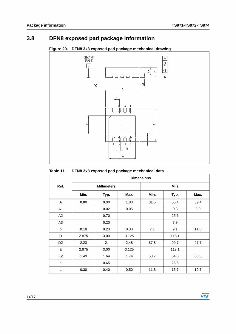
3.8 DFN8 exposed pad package information
Figure 20. DFN8 3x3 exposed pad package mechanical drawing
Table 11. DFN8 3x3 exposed pad package mechanical data
Ref.
Dimensions
Millimeters Mils
Min. Typ. Max. Min. Typ. Max.
A 0.80 0.90 1.00 31.5 35.4 39.4
A1 0.02 0.05 0.8 2.0
A2 0.70 25.6
A3 0.20 7.9
b 0.18 0.23 0.30 7.1 9.1 11.8
D 2.875 3.00 3.125 118.1
D2 2.23 2. 2.48 87.8 90.7 97.7
E 2.875 3.00 3.125 118.1
E2 1.49 1.64 1.74 58.7 64.6 68.5
e 0.65 25.6
L 0.30 0.40 0.50 11.8 15.7 19.7

TS971-TS972-TS974 Ordering information
15/17
4 Ordering information
Table 12. Order codes
Order codeTemperature
rangePackage Packing Marking
TS971IDTS971IDT
-40°C, +125°C
SO-8Tube or
Tape & reel971I
TS971ILT SOT23-5L
Tape & reel
K120
TS971IYD(1)
TS971IYDT(1)SO-8
(Automotive grade level)971IY
TS971IYLT(2) SOT23-5L(Automotive grade level)
K121
TS972IN DIP8 Tube TS972IN
TS972ID
TS972IDTSO-8
Tube orTape & reel
972ITS972IPTTSSOP8
(Thin shrink outline package)Tape & Reel
TS972IQTDFN8
(Dual micro lead frame package)
TS972IYD(1)
TS972IYDT(1)SO-8
(Automotive grade level)Tube or
Tape & reel972IY
TS972IYPT(2) TSSOP8(Automotive grade level)
Tape & reel 972IY
TS974IN DIP14 Tube TS974IN
TS974IDTS974IDT
SO-14Tube or
Tape & reel974I
TS974IPTTSSOP14
(Thin shrink outline package)
Tape & reelTS974IYD(1)
TS974IYDT(1)SO-14
(Automotive grade level)974IY
TS974IYPT(2) TSSOP14
(Automotive grade level)974IY
1. Qualified and characterized according to AEC Q100 and Q003 or equivalent, advanced screening according to AEC Q001 & Q 002 or equivalent.
2. Qualification and characterization according to AEC Q100 and Q003 or equivalent, advanced screening according to AEC Q001 & Q 002 or equivalent are on-going.

Revision history TS971-TS972-TS974
16/17
5 Revision history
Table 13. Document revision history
Date Revision Changes
15-Nov- 2002 1 First release.
9-May- 2005 2 Modifications on AMR table (explanation of Vid and Vi limits)
31-Aug-2005 3 PPAP references inserted in the datasheet, see Table 1 on page 2.
9-Dec-2005 4Thermal resistance junction to case data added in Table 1. on page 2
Missing PPAP references inserted in the datasheet, see Table 12: Order codes.
3-Oct-2007 5
Added Rthja and Rthjc values for DIP8 and DIP14 packages in Table 1.
ESD footnotes updated in Table 1: Absolute maximum ratings AMR.Description section updated on cover page.
Markings for automotive grade parts corrected in Table 12: Order codes.
20-Dec-2007 6Reformatted package information in Section 3: Package information.
Footnotes for automotive grade parts corrected in Table 12: Order codes.
TS971-TS972-TS974
17/17
Please Read Carefully:
Information in this document is provided solely in connection with ST products. STMicroelectronics NV and its subsidiaries (“ST”) reserve theright to make changes, corrections, modifications or improvements, to this document, and the products and services described herein at anytime, without notice.
All ST products are sold pursuant to ST’s terms and conditions of sale.
Purchasers are solely responsible for the choice, selection and use of the ST products and services described herein, and ST assumes noliability whatsoever relating to the choice, selection or use of the ST products and services described herein.
No license, express or implied, by estoppel or otherwise, to any intellectual property rights is granted under this document. If any part of thisdocument refers to any third party products or services it shall not be deemed a license grant by ST for the use of such third party productsor services, or any intellectual property contained therein or considered as a warranty covering the use in any manner whatsoever of suchthird party products or services or any intellectual property contained therein.
UNLESS OTHERWISE SET FORTH IN ST’S TERMS AND CONDITIONS OF SALE ST DISCLAIMS ANY EXPRESS OR IMPLIEDWARRANTY WITH RESPECT TO THE USE AND/OR SALE OF ST PRODUCTS INCLUDING WITHOUT LIMITATION IMPLIEDWARRANTIES OF MERCHANTABILITY, FITNESS FOR A PARTICULAR PURPOSE (AND THEIR EQUIVALENTS UNDER THE LAWSOF ANY JURISDICTION), OR INFRINGEMENT OF ANY PATENT, COPYRIGHT OR OTHER INTELLECTUAL PROPERTY RIGHT.
UNLESS EXPRESSLY APPROVED IN WRITING BY AN AUTHORIZED ST REPRESENTATIVE, ST PRODUCTS ARE NOTRECOMMENDED, AUTHORIZED OR WARRANTED FOR USE IN MILITARY, AIR CRAFT, SPACE, LIFE SAVING, OR LIFE SUSTAININGAPPLICATIONS, NOR IN PRODUCTS OR SYSTEMS WHERE FAILURE OR MALFUNCTION MAY RESULT IN PERSONAL INJURY,DEATH, OR SEVERE PROPERTY OR ENVIRONMENTAL DAMAGE. ST PRODUCTS WHICH ARE NOT SPECIFIED AS "AUTOMOTIVEGRADE" MAY ONLY BE USED IN AUTOMOTIVE APPLICATIONS AT USER’S OWN RISK.
Resale of ST products with provisions different from the statements and/or technical features set forth in this document shall immediately voidany warranty granted by ST for the ST product or service described herein and shall not create or extend in any manner whatsoever, anyliability of ST.
ST and the ST logo are trademarks or registered trademarks of ST in various countries.
Information in this document supersedes and replaces all information previously supplied.
The ST logo is a registered trademark of STMicroelectronics. All other names are the property of their respective owners.
© 2007 STMicroelectronics - All rights reserved
STMicroelectronics group of companies
Australia - Belgium - Brazil - Canada - China - Czech Republic - Finland - France - Germany - Hong Kong - India - Israel - Italy - Japan - Malaysia - Malta - Morocco - Singapore - Spain - Sweden - Switzerland - United Kingdom - United States of America
www.st.com