Embed Size (px)
Citation preview

Orthogonal Polarization Agile Planar Array Antenna
September 2010
Department of Engineering Systems and Technology Graduate School of Science and Engineering
Saga University
Sen Feng

i
Acknowledgement
I would especially like to express my most sincere thanks to my advisor,
Professor Masayoshi Aikawa, for his invaluable guidance, advice, encouragement and support throughout the completion of my study and this thesis. I would also like to express my appreciation to the members of my thesis committee, Professor Kohei Arai, Professor Tatsuya Furukawa, Associate Professor Sumio Fukai and Associate Professor Shinichi Sasaki for their kind assistance and valuable instruction.
Special appreciation is also designated to Lecturer Takayuki Tanaka,
Assistant Professor Eisuke Nishiyama and Mr. Tasuku Uechi for their kind assistance.
Then I want to thank to all my lab-mates for their kindness, direct and
indirect support and making these past years of working together an enjoyable time.
Last but not least, a very big thank you to my beloved parents and
friends in China, for their genuine support and constant encouragement they have bestowed upon me throughout my study in Japan.

ii
Abstract
In the recent years, along with the rapid progress of wireless communication
technology, wireless equipments have been widely applied to various practical fields such
as Global Positioning System (GPS), Wireless Local Networking Systems, and wireless
access systems and so on. The main requirements of these wireless equipments are the
better performance, low cost and small size.
Due to various functionalities as well as lightness, low profile and easy fabrication
properties, microstrip planar antennas are well suited for any wireless equipment. As an
important requirement of planar antennas, the polarization agility technique is a typical and
good candidate in advanced wireless communication systems because of its promising
capability.
In this study, therefore, a novel three conductive layers 2×2 ring-slot array antenna is
designed and utilized to realize the simultaneous use of the orthogonal linear polarizations.
Due to the use of the characteristics of the ring-slot array antenna and features of the
both-sided MIC technology, excellent performances such as broad-band, good isolation,
and better cross polarization suppression are obtained. For the symmetrical antenna
structure, two orthogonal linear polarizations can be realized with same radiation pattern
and same polarization performance. In addition, the antenna design is very simple, and the
array antenna is easy to fabricate.
Using the characteristics of the ring-slot array antenna mentioned above, a novel
circular polarization ring-slot array antenna with simultaneous use of the orthogonal
polarizations is proposed. By integrating a broad-band 90 degrees hybrid circuit, the array
antenna can radiate two kinds of circular polarizations; that is, Left Hand Circular
Polarization (LHCP) and Right Hand Circular Polarization (RHCP) with good polarization
performance. Moreover, the circular polarization can be obtained in a very wide frequency
range. The 3 dB axial ratio bandwidths are wider than 25% (RHCP) and 29% (LHCP) and
the impedance bandwidth is 47%.
And then a novel linear polarization switchable ring-slot array antenna structure has
been developed. Basing on the study of three conductive layers ring-slot array antenna, a
Single Pole Double Throw (SPDT) switch circuit is integrated in the array antenna to
compose an advanced array antenna, linear polarization switchable array antenna. By using

iii
the SPDT switch circuit, the antenna can provide the switching function between the φ = +45 degree and φ = -45 degree linear polarization. In this array antenna, ±45 degree
linear polarization can be realized with excellent cross polarization suppression better than
-20 dB.
Finally, a 90 degrees branch line hybrid circuit and a SPDT switch circuit are
integrated in the ring-slot array antenna to form a novel circular polarization switchable
ring-slot array antenna. The orthogonal circular polarizations can be switched with simple
method. And the orthogonal circular polarization switchable ring-slot array antenna is
theoretically and experimentally verified.
These results are very promising and suited for wireless communication systems and
RF sensors, which need orthogonal polarization agility.

iv
Publications International Journal (Refereed) [1] Sen Feng, Eisuke Nishiyama, Masayoshi Aikawa, “ Broad-band circularly
polarized ring-slot array antenna for simultaneous use of the orthogonal
polarizations, ” IEICE TRANS. ELECTRON., vol. E93-C, no 7, pp. 1105-1110,
July 2010.
[2] Sen Feng, Eisuke Nishiyama, Masayoshi Aikawa, “ Linear polarization switchable
ring-slot array antenna using SPDT switch circuit, ” To be published in IET
MICROWAVES, ANTENNA & PROPAGATION.
Proceedings of International Conference (Refereed) [1] Sen Feng, Eisuke Nishiyama, Masayoshi Aikawa, " A wideband dual circularly
polarized array antenna by using microwave multi layer technology," Proc. of the
International Symposium on Antennas and propagation (ISAP), pp.892 - 895,
Niigata, Japan, August 2007.
[2] Sen Feng, Eisuke Nishiyama, Masayoshi Aikawa, “ Linear polarization switchable
slot ring array antenna with SPDT switch circuit, ” Proc. of the 2009 Asia-Pacific
Microwave Conference (APMC2009), pp.1828, Singapore, Dec. 2009.
Conference Paper in Domestic Session [1] Sen Feng, Eisuke Nishiyama, and Masayoshi Aikawa, " Circularly Polarized
Microstrip Array Antenna by using Hybrid Multi Layer Circuits, " ITE Technical
Report,BCT2007-21, pp.83-86, Kumamoto, Japan, Jan. 2007.

v
[2] Sen Feng, Eisuke Nishiyama, and Masayoshi Aikawa, " Polarization switchable
slot ring array antenna by using microwave multi layer technology, " Proc. Of the conference of electronic and electronics engineers in Kyushu, no. 61, pp. 03-2A-05, 2008.

vi
CONTENTS
Acknowledgments
Abstract Publications
i
ii
iv
Contents
vi
Chapter 1 Introduction 1 1.1 Introduction to Polarization Agile Planar Antenna…………………………... 1
1.2 Focus of Study………………………………………………………………... 2
Chapter 2 Planar Antenna using Both-Sided MIC Technology 5
2.1 Microstrip Slot Antenna………………………..…………………………….. 5
2.2 Antenna Array……………...……………………….……….……………….. 8
2.3 Polarization…………………...……………………………………………… 10
2.4 Circularly Polarized…...…...………………………………………………… 14
2.5 Both-Sided MIC Technology…….…………………………………………... 16
2.5.1 Features of Both-Sided MIC Technology……………………………… 16
2.5.2 Branch Circuit using Both-Sided MIC Technology ………………….... 18
2.5.3 Comparing A Conventional Antenna with An Antenna using
Both-Sided MIC Technology…………………………………………... 20
2.5.4 Three Layers Orthogonal Resonating Feed Circuit using
Both-Sided MIC technology…………………………………………… 22
Chapter 3 Broad-Band Linear Polarization Ring-Slot Array Antenna with Simple Structure 24
3.1 Introduction....................................................................................................... 24
3.2 Antenna Design Procedure and Simulation………………………………….. 25
3.3 Experimental Results and Discussion………………………………………... 29

vii
3.4 Conclusion…………………………………………………………………… 34
Chapter 4 Circularly Polarized Ring-Sot Array Antenna for Simultaneous use of The Orthogonal Polarizations 35
4.1 Introduction…………………………………………………………………... 35
4.2 Circularly Polarized Ring-slot Array Antenna Using
π/2 Hybrid Circuit…………………………………………………………… 36
4.3 Broad-Band Microstrip π/2 Hybrid Circuit………………………………….. 40
4.4 Experiment…………………………………………………………………… 42
4.5 Conclusion…………………………………………………………………… 47
Chapter 5 Linear Polarization Switchable Ring-Slot Array
Antenna using SPDT Circuit 485.1 Introduction…………………………………………………………………... 48
5.2 Design of Ring-Slot Array Antenna For Linear
Polarization Switching……………………………………………………….
49
5.2.1 Antenna Configuration…..……………………………………………... 49
5.2.2 SPDT Switch Circuit…………………………………………………… 51
5.3 Experimental Results and Discussion………………………………………...
5.4 Conclusion……………………………………………………………………
55
59
Chapter 6 Circularly Polarized Switchable Ring-Slot Array Antenna with Broad-Band 61
6.1 Introduction…………………………………………………………………...
6.2 Principle of Proposed Ring-Slot Array Antenna………………………….......
6.2.1 Antenna Design…………………………………………………………
6.2.2 Microstrip Branch Line Hybrid Circuit
with SPDT Switch Circuit……………………………………………....
6.3 Experimental Results………………………………………….……………...
6.4 Conclusion……………………………………………………………………
61
62
62
64
67
70
Chapter 7 Conclusion
72
References 74
1
Chapter 1
Introduction
1.1 Introduction to Polarization Agile Planar Antenna
Along with the rapid development of wireless communication technology, wireless
equipments have been widely applied to various practical fields such as Wireless Local
Networking Systems (WLAN), Global Positioning System (GPS), modern
communications, Synthetic Aperture Radars (SAR), RF sensors, wireless access
systems and so on. The main requirements of these wireless equipments are the better
performance, low cost and advanced functions.
Due to various functionalities as well as lightness, low profile and easy fabrication
properties, microstrip planar antennas are well suited for any wireless equipment.
Moreover, in the present day, applications in wireless systems usually require
orthogonal polarization agile and broadband performance in order to meet the
miniaturization requirements of mobile units. Thus, orthogonal polarization agile,
bandwidth enhancement and advanced functions have become the subjects of great
interest to the antenna engineering designers. For these reasons, studies to achieve
orthogonal polarization agile and broadband operations of microstrip planar antennas
have greatly increased. Much significant progress in the design of microstrip planar
antennas with broadband, dual polarization, circular polarization using microwave
function circuits or semiconductor devices have reported [1]-[3]. In these papers,
antennas are integrated with a function circuit or semiconductor device such as diode,
and the integrated planar antenna can realize the polarization agile and broadband
performance.
However, these planar antennas are only the development of the single element
antenna with polarization agile and broadband performance. The investigation of the
array antenna with orthogonal polarization agile and broadband performance has not
2
been involved. In addition, these antennas have the drawback of unsatisfactory
performance of the low speed orthogonal polarization switching due to the adjustment
of the antenna resonate mode. And the structure of these antennas is relatively
complicated. Therefore, it will be very beneficial that the array antenna could be
integrated with a high speed, broadband feeding circuit with simple circuit structure.
1.2 Focus of Study
In this study, four kinds of array antennas with polarization agility and wide
bandwidth are proposed. Figure 1 shows the basic flow of this thesis.
Firstly, a novel three conductive layers 2×2 ring-slot array antenna is designed and
utilized to realize the simultaneous use of the orthogonal linear polarizations. Due to the
use of the characteristics of the ring-slot array antenna and features of the both-sided
MIC technology, excellent performances such as broad-band, good isolation, and better
cross polarization suppression are obtained. For the symmetrical antenna structure, two
orthogonal linear polarizations can be realized with same radiation pattern and same
polarization performance. In addition, the antenna design is very simple, and the array
antenna is easy to fabricate.
Using the characteristics of the ring-slot array antenna mentioned above, a novel
circular polarization ring-slot array antenna with simultaneous use of the orthogonal
polarizations is proposed. By integrating a broad-band 90 degrees hybrid circuit, the
array antenna can radiate two kinds of circular polarizations; that is, Left Hand Circular
Polarization (LHCP) and Right Hand Circular Polarization (RHCP) with good
polarization performance. Moreover, the circular polarization can be obtained in a very
wide frequency range. The 3 dB axial ratio bandwidths are wider than 25% (RHCP) and
29% (LHCP) and the impedance bandwidth is 47%.
Moreover, a novel linear polarization switchable ring-slot array antenna structure
has been developed. Basing on the study of three conductive layers ring-slot array
antenna, a Single Pole Double Throw (SPDT) switch circuit is integrated in the array
antenna to compose an advanced array antenna, linear polarization switchable array
antenna. By using the SPDT switch circuit, the antenna can provide the switching
function between the φ = +45 degree and φ = -45 degree polarization. In this array antenna, ±45 degree polarization can be realized with excellent cross polarization

3
suppression better than -20 dB.
In addition, a 90 degrees branch line hybrid circuit and a SPDT switch circuit are
integrated in the ring-slot array antenna to form a novel circular polarization switchable
ring-slot array antenna. The two kinds of circular polarizations can be switched with
simple method. And the orthogonal circular polarization switchable ring-slot array
antenna is theoretically and experimentally verified.
These results are very promising and suited for wireless communication systems and
RF sensors, which need the orthogonal polarization agility.

4
Figure 1 Basic flow of this thesis
5
Chapter 2
Planar Antenna using Both-Sided MIC Technology
Along with the rapid development of wire less communication technology,
microwave planar antennas have been widely applied to various practical fields.
Microwave integrated slot array antennas are a vital part of the microwave planar
antennas and widely used in the wireless communication equipments. In addition, by
the progress of the MIC technology, the researchers [4]-[5] and several other researchers
have developed “Both-Sided MIC’s technology” which effectively utilizes the several
microwave transmission lines on both sides of the substrate. In this chapter, the
microwave planar antenna using both-sided MIC’s technology is described.
2.1 Microstrip Slot Antenna
Microstrip slot antenna plays an important role in the microwave planar antenna.
Microstrip slot antennas are composed of a slot in the ground plane of a substrate and
excited by a microstrip line. Many types of slot antennas have been extensively
discussed in [6]-[10]. The advantage of these slot antennas is shown as follows:
Slot antennas can produce bidirectional and unidirectional radiation with
comparatively wide frequency bandwidth.
Microstrip line and slot combinations offer an additional degree of freedom in the
design of microstrip antennas.
Slot antennas with desired polarization can be produced, and they are less sensitive
to manufacturing tolerances than are microstrip patch antennas.
Miniaturization potential.

6
The antenna design is practically easy.
Basically, there are two kinds of aspects in the design of slot antenna, that is,
microstrip fed rectangular slot antenna and the ring slot antenna. The two kinds of slot
antennas are described briefly in this section.
Microstrip fed rectangular slot antenna
A microstrip slot antenna is composed of a slot cut in the ground plane of the
microstrip line, where the slot is perpendicular to the strip conductor of the microstrip
line. The fields of the microstrip line excite the slot. For efficient excitation of the slot,
the strip conductor is shorted either through the using of a via hole as shown in Figure
2.1 (a) or through the using of an open circuited stub beyond the edge of the slot as
shown in Figure 2.1 (b). A center-fed slot antenna has a very high radiation resistance,
and a matching network may be needed to match the antenna to the characteristic
impedance of the microstrip line.
(a) (b)
Figure 2.1 Structure of the microstrip fed rectangular slot antenna

7
This type of slot antennas has been studied theoretically and experimentally by
many researchers [11]-[16]. The microstrip fed slot antenna has the advantage of very
low cross polarization. In addition, much wider applications can be found if a metallic
reflector is added for a directional radiation pattern.
However, due to the antenna structure, this type of slot antenna is difficult to realize
the circular polarization.
Ring slot antenna
A ring slot antenna is composed of a circular slot in the ground plane of a dielectric
substrate, and fed by a microstrip line as shown in Figure 2.2. This type of slot antenna
is very suited for the mobile communications as a vehicular antenna, since it can radiate
power at low elevation angles [17].
Using a dual-feed design, the circular polarization can be easily realized from the
ring slot antenna. The dual-feed design can be based on a typical hybrid circuit. The ring
slot antenna exciting two orthogonal polarization modes by using the dual-feed circuit,
and the two modes have same amplitude with 90 degrees phase difference. Moreover,
the radiation patterns of the ring slot antenna can be controlled easily by loading the slot
with a tunable capacitor [18].
Figure 2.2 Structure of the microstrip fed ring slot antenna

8
However, most of the ring slot antenna has been discussed with one antenna element
so far, and there is no report that investigates ring slot array antennas with circular
polarization.
2.2 Antenna Array
In the conventional microstrip antennas, characteristics such as high gain, beam
scanning or steering capability are possible only when discrete radiation are combined
to form arrays. The elements of an array may be spatially distributed to form a linear,
planar, or volume array. A linear array consists of elements located finite distances apart
along a straight line. A planar array has elements distributed on a plane and a volume
array has elements that are distributed in three dimensions.
In this section, two kinds of the most usefully array, that is, the one-dimensional
parallel feed array and the two-dimensional parallel feed array are described.
One-dimensional parallel feed array
Figure 2.3 shows the fundamental configuration of a one-dimensional parallel feed
array.
Figure 2.3 One-dimensional parallel feed array
This array consists of branching networks of two way power dividers. A corporate
feed is the most widely used parallel feed configuration. In this parallel feed array, the
power is divided equally at each junction. However, different power divider ratios can

9
be chosen to generate a tapered distribution across the array. If the distances from the
input port to each radiating element are identical, the beam position is independent of
the frequency and the feed is broadband.
In this type of array, basically, the T-junction or its modified configuration is used as
a power divider. The quarter-wave transformers are generally utilized to obtain
impedance match at the junction.
Two-dimensional parallel feed array
The configuration of two-dimensional parallel feed array is shown in Figure 2.4.
The basic configuration can be extended to large arrays with specifically 2ⁿ elements
per side to maintain a symmetrical configuration. Some works on application of this
type of array have been presented [19]-[20].
Figure 2.4 Two-dimensional parallel feed array
10
)(tan1
21
EE−=γ 00 900 ≤≤ γ
2.3 Polarization
Antenna can radiate three kinds of polarizations, that is, linear, elliptic, or circular
polarizations. If the path of the electric field vector is back and forth along a line, it is
said to be linearly polarized. As Figures 2.5 (a) and (b) shows, in actual space above the
earth, if the electric vector is vertical or lies in a vertical plane, the wave is said to be
vertically polarized; if the electric vector lies in a horizontal plane, the wave is said to
be horizontally polarized. If the electric field vector remains constant in length but
rotates around in a circular path, it is circularly polarized. The rotation radian frequency
is ω and occurs in one of two directions, referred to as the sense of rotation. If the wave is traveling toward the observer and the vector rotates counterclockwise, it is right-hand
polarization. If it rotates clockwise, it is left-hand polarization. Right-hand and left-hand
circularly polarized waves are shown in Figures 2.5 (c) and (d). A circularly polarized
wave can be realized when two linearly polarized waves are combined, that is, if they
are simultaneously launched in the same direction from the same antenna-provided that
the two linear polarization are at right angles to each other and their phase difference is
90 degrees. The right-hand or left-hand rotation depends on whether the phase
difference is 90 degrees or -90 degrees. Moreover, for circular polarization it is
necessary also that the two linearly polarized components by equal amplitude. Finally, a
wave may be elliptically polarized, with either right- or left-hand sense of rotation, as
shown in Figures 2.5 (e) and (f).
A general polarization ellipse is shown in Figure 2.6 with a reference axis system,
where the wave associated with this polarization ellipse is traveling in the +z-direction.
The sense of rotation can be either left or right. The instantaneous electric field vector ε has components εx and εy along the x and y axes. The peak values of these components are E1 and E2. The angle γ describes the relative values of E1 and E2 form
(2.1)
The tilt angle of the ellipse, τ, is angle between the x-axis (horizontal) and the major
axis of the ellipse. The angle ω’ is seen from Figure 2.6 to be
(2.2) )(cot' 1 AR−=ω ∞≤≤ ||1 AR oo 45'45 ≤≤− ω
oo 900 ≤≤ γ
oo 45'45 ≤≤− ω

11
ε
ε
(a) (b)
ε ε
(c) (d)
ε ε
(e) (f)
Figure 2.5 Polarization states. The wave is approaching. (a) Linear
(vertical) polarization. (b) Linear (horizontal) polarization (c) Right-hand
circular polarization. (d) Left-hand circular polarization. (e) Right-hand
elliptical polarization (f) Left-hand elliptical polarization

12
The axial ratio of the ellipse |AR| is the ratio of the major axis (OA) electric field
component to the minor axis (OB) electric field component, where
(2.3)
(2.4)
The sign of AR is positive for left-hand sense and negative for right- hand sense.
The instantaneous electric field for the wave of Figure 2.6 can be written as (with z
= 0 for simplicity)
(2.5)
Where δ is the phase by which the y-component leads the x-component, and the ,x y
are the radial unit vectors. This representation describes the ellipse shape as time
progresses.
Figure 2.6 The general polarization ellipse. The associated wave direction is out of the
page in the +z-direction. The tip of the instantaneous electric field vector ε traces out the ellipse
( ) ytExtEyx yx ˆ)cos(ˆcosˆˆ 21 δωωεεε ++=+=
( )2/1
2/122
21
42
41
22
21 ]2cos2[
21
⎥⎦⎤
⎢⎣⎡ ++++= δEEEEEEOA
( )2/1
2/122
21
42
41
22
21 ]2cos2[
21
⎥⎦⎤
⎢⎣⎡ ++−+= δEEEEEEOB

13
Linear Polarization
If the components are in phase (δ =0) the net vector is linearly polarized. The
orientation of the linear polarization depends on the relative values of E1 and E2. For
example, if E1= 0 vertical linear polarization results; if E2 = 0 horizontal linear results.
By summarize the linear polarization; this kind of polarization can be accomplished
if the field vector (electric or magnetic) possesses:
a. Only one component
b. Two orthogonal linear components that are in phase or 180°(or multiples of
180°) out of phase.
Elliptical Polarization
If E1 = E2, the polarization is linear at 45o with respect to the axes. Linear
polarization is a collapsed ellipse with infinite axial ratio. If δ is nonzero, the axial ratio
is finite. When δ > 0, εy leads εx in phase and the sense of rotation is left hand. For δ <0 the sense is right hand.
The necessary and sufficient conditions to accomplish elliptical polarization are if
the field vector (electric or magnetic) possesses all of the following:
a. The field must have two orthogonal linear components.
b. The two components can be of the same or different magnitude.
c. (1) If the two components are not of the same magnitude, the time-phase difference between the two components must not be 0°or multiples of 180° (because it will
then be linear). (2)If the two components are of the same magnitude, the time-phase
difference between the two components must not be odd multiples of 90°(because
it will then be circular).
Circular Polarization
If E1 = E2 and δ = ±90°, the polarization is circular (+ 90o is LHCP, and -90o is
RHCP). The axial ration or a circularly polarized wave is unity.

14
The necessary and sufficient conditions to accomplish circular polarization are if the
field vector (electric or magnetic) possesses all of the following:
a. The field must have two orthogonal linear components.
b. The two components must have the same magnitude.
c. The two components must have a phase difference of odd multiples of 90°.
2.4 Circularly Polarized Antenna
It is usually designed for single-mode operation that radiates mainly linear
polarization. For radiating a circular polarization, an antenna must support orthogonal
fields of equal amplitude with 90° phase difference. This requirement can be
accomplished by a single patch with proper excitations or by a patch array with an
appropriate arrangement and phasing.
Two Fed Circularly Polarized Antenna
The fundamental configurations of a two fed circularly polarized patch using an
external power divider are shown in Figure 2.7.
(a) Circular patch (b) Square patch
Figure 2.7 Typical configurations of two-fed circularly polarized microstrip antennas
The antenna patch is usually square or circular. The dual-orthogonal feeds excite two
orthogonal modes with equal amplitude with 90°phase difference. Several power

15
divider circuits that have been successfully employed for CP generation include the
quadrature hybrid, the ring hybrid, the Wilkinson power divider, and the T-junction
power splitter [21]. The power divider circuit divides the input RF signal into two
outputs with equal amplitude and 90 degrees phase difference.
Singly Fed Circularly Polarized Antenna
Typical configurations for singly fed CP microstrip antennas are shown in Figure 2.8.
A single-point feed patch capable of producing CP radiation is very desirable in
situations where it is difficult to accommodate dual-orthogonal feeds with a power
divider network. Because a patch with a single-point feed generally radiates linear
polarization, in order to radiate CP, it is necessary for two orthogonal patch modes with
equal amplitude and with 90°phase difference to be induced. This can be accomplished
by slightly perturbing a patch at appropriate locations with respect to the feed.
The singly fed circularly polarized microstrip antennas operate on the principle of
detuning degenerate modes of a symmetrical patch by perturbation segments as shown
in Figure 2.9. The fields of a singly fed patch can be resolved into two orthogonal
degenerate modes, #1 and #2. Proper perturbation segments will detune the frequency
response of mode #2 such that, at the operating frequency f0, it is the same amplitude
and 90 degrees phase difference with respect to mode #1. Therefore, the two modes
satisfy the required condition for CP radiation. The detail explanation is done in
[22]-[24].
(a) Square patch (b) Circular patch
Figure 2.8 Typical configurations of singly fed circularly polarized
microstrip antennas

16
∞≤≤ AR1
.
Figure 2.9 Amplitude and phase of orthogonal modes for singly fed circularly
polarized microstrip antennas.
The axial ratio is the key characteristic to the circular polarization. The ratio of the
major axis to the minor axis is referred to as the axial ratio (AR). The axial ratio is
generally used to specify the quality of the circularly polarized waves. As shown in
Figure 2.6, the axial ratio is equal to
, (2.6)
In general, the unit of axial ratio is dB (10log10|AR|). In a pure circular polarization,
the AR is 1 or 0 dB.
2.5 Both-Sided MIC Technology 2.5.1 Features of Both-Side MIC Technology
The both-sided MIC’s technology has many practical advantages due to the effects
of combining several kinds of transmission lines, and the effective use of both sides of
the substrate. The advantages are as follows:
)()( OB
OAaxisMinoraxisMajorAR ==
17
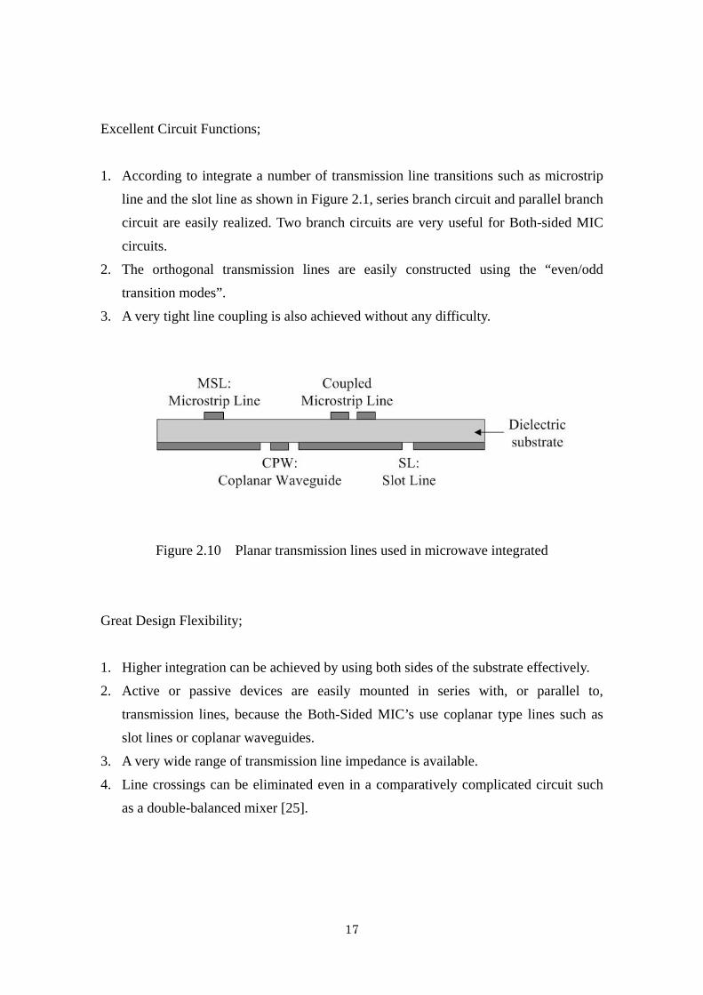
Excellent Circuit Functions;
1. According to integrate a number of transmission line transitions such as microstrip
line and the slot line as shown in Figure 2.1, series branch circuit and parallel branch
circuit are easily realized. Two branch circuits are very useful for Both-sided MIC
circuits.
2. The orthogonal transmission lines are easily constructed using the “even/odd
transition modes”.
3. A very tight line coupling is also achieved without any difficulty.
Figure 2.10 Planar transmission lines used in microwave integrated
Great Design Flexibility;
1. Higher integration can be achieved by using both sides of the substrate effectively.
2. Active or passive devices are easily mounted in series with, or parallel to,
transmission lines, because the Both-Sided MIC’s use coplanar type lines such as
slot lines or coplanar waveguides.
3. A very wide range of transmission line impedance is available.
4. Line crossings can be eliminated even in a comparatively complicated circuit such
as a double-balanced mixer [25].
18
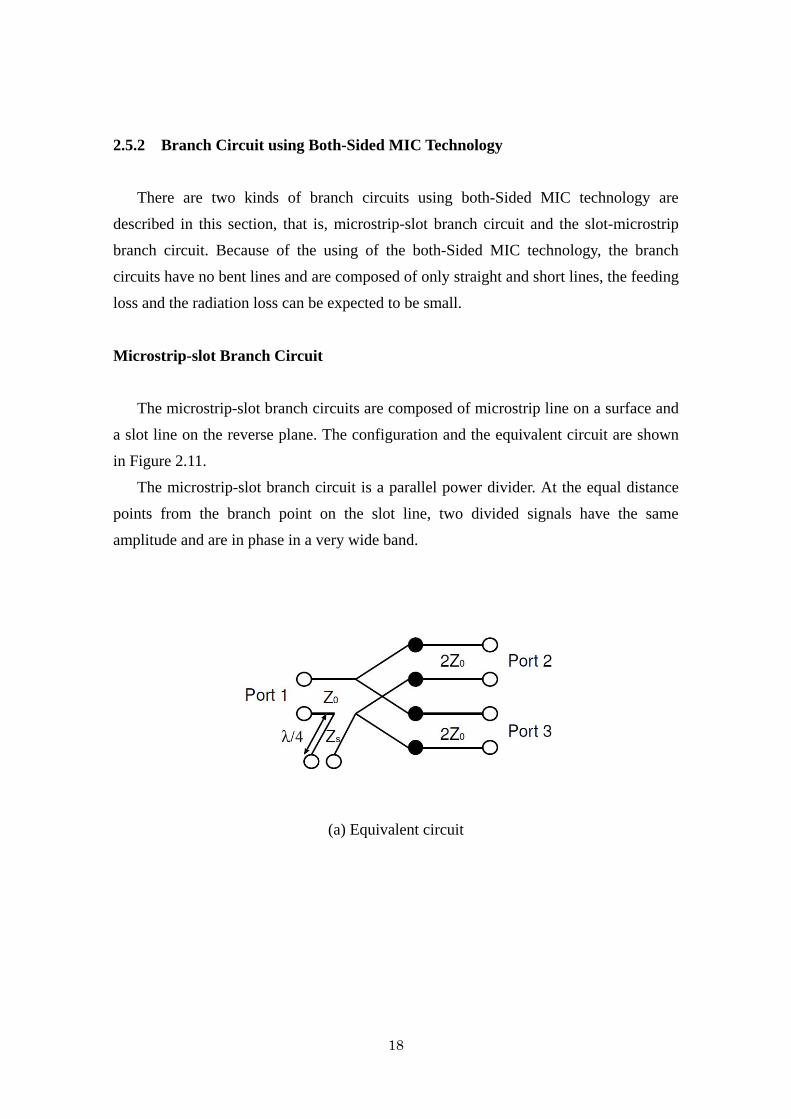
2.5.2 Branch Circuit using Both-Sided MIC Technology
There are two kinds of branch circuits using both-Sided MIC technology are
described in this section, that is, microstrip-slot branch circuit and the slot-microstrip
branch circuit. Because of the using of the both-Sided MIC technology, the branch
circuits have no bent lines and are composed of only straight and short lines, the feeding
loss and the radiation loss can be expected to be small.
Microstrip-slot Branch Circuit
The microstrip-slot branch circuits are composed of microstrip line on a surface and
a slot line on the reverse plane. The configuration and the equivalent circuit are shown
in Figure 2.11.
The microstrip-slot branch circuit is a parallel power divider. At the equal distance
points from the branch point on the slot line, two divided signals have the same
amplitude and are in phase in a very wide band.
(a) Equivalent circuit

19
(b) Configuration of microstrip-slot branch circuits
Figure 2.11 Microstrip-slot branch circuits
Slot-microstrip Branch Circuit
Figure 2.12 shows the configuration and equivalent circuit for a slot-microstrip
branch circuit. The slot-microstrip branch circuit is a series power divider. At the equal
distance points from the branch point on the microstrip line, two divided signals have
the same amplitude and are out of phase in a very wide band.
(a) Equivalent circuit

20
(b) Configuration of slot-microstrip line
Figure 2.12 Slot-microstrip branch circuits
2.5.3 Comparing a Conventional Antenna with an Antenna Using Both-Sided
MIC Technology
Feed circuits for conventional microstrip array antennas have been usually
composed of the microstrip-line (Figure 2.13). In this case, since all the feeding circuits
are connected in parallel, many matching circuits are required. As a result, the feeding
circuit layout for the array antennas become complicated and the length of the feed lined
become much longer. Those cause the array antennas to increase the feeding loss as well
as an undesired radiation.
A microstrip array antenna by using Both-Sided MIC technology is shown in Figure
2.14. By using the Both-Sided MIC technology for the feeding circuits, the array
antenna needs no impedance matching circuits and has very simple circuit configuration,
which are mainly due to the excellent performances of both the microstrip-slot parallel
branch circuit and the slot-microstrip series branch circuit. And the feeding loss and the
radiation loss can be expected to be small because for the feeding circuits have no bent
lines and are composed of only straight and short lines.

21
Figure 2.13 Conventional microstrip array antenna.
Figure 2.14 Microstrip array antenna using Both-Sided MIC technology

22
2.5.4 Three Layers Orthogonal Resonating Feed Circuit using Both-Sided MIC
Technology
Using the Both-sided MIC technology, a three layers orthogonal resonating feed
circuit is proposed. Figure 2.15 (a) shows the configuration of the three layers feed
circuit, which consist of two layer dielectric substrates, three conductive layers and two
input ports. The upper feed circuit is constructed with Port-I and microstrip line on the
upper layer. The lower feed circuit is constructed with Port-II and microstrip line on the
lower layer. The cross slot lines on the middle layer are the dual-use for both the upper
feed circuit and the lower feed circuit.
When a RF signal is fed to the feed circuit from Port-I / Port-II, the signals are
divided in parallel (in phase) to the two cross-slots by the upper feed circuit / lower feed
circuit. Using the microstrip-slot branch circuit, the RF signal is fed to the slot line
which perpendicular to the feed microstrip line. Since the RF signals in the slot line are
in phase as shown in Figure 2.15 (b), the cross slot line which parallel to the feed
microstrip line is not be excited in principle.
(a)

23
Fed by Prot-I Fed by Port-II
(b)
Even mode transmission (A-A’) Odd mode transmission (A-A’)
(c)
Figure 2.15 Configuration of the three layers orthogonal resonating feed circuit
In addition, there are two ways of exciting the three layers feed circuit, that is, even
mode transmission and the odd mode transmission as shown in Figure 2.15 (c). The two
kinds of transmission modes are orthogonal to each other.
Therefore, the excellent isolation performance between the two feed pots of the
proposed three layers feed circuit based on the both-sided MIC technology can be
obtained.

24
Chapter 3
Broad-Band Linear Polarization Ring-Slot Array Antenna with Simple Structure
3.1 Introduction
Modern wireless communication systems, such as those for satellite for satellite
links (GPS, vehicular, etc.), for mobile communication, and for emerging applications,
such as wireless local-area networks (WLANs), often require compact antennas at low
cost. Further, due to their various functionalities as well as lightness, low profile and
easy fabrication properties, microwave planar antennas are well suited for airborne
applications, such as synthetic aperture radar (SAR) systems.
Therefore, the microwave slot antennas are attracting much attention in various
wireless communication systems due to their miniaturization potential, wide band and
low cost recently. In addition, dual polarization operation is an important subject in slot
antenna design. Several microwave slot antennas are reported to achieve improved
performance, particularly for broadband and dual polarization applications. In [26]-[27],
microwave slot antennas are reported to obtained broadband polarization. In [28]-[29],
dual polarization is obtained by a feed network and two ports.
In this chapter, a novel broad-band linear polarization ring-slot array antenna is
described. The two orthogonal linear polarizations can be realized simultaneously by
using proposed antenna. The both-sided MIC technology as mentioned in last chapter is
effectively employed in forming this proposed slot array antenna. By using this
technology, an excellent isolation between two input ports and very simple circuit
configuration is achieved.
As a fundamental research of ring-slot array antenna, the simulated and measured
characteristics of the proposed array antenna are described in this chapter. And both the

25
simulation results and the experimental results show that the proposed array antenna has
good polarization characteristics for the two orthogonal linear polarizations.
3.2 Antenna Design Procedure and Simulation
The structure of the proposed broad-band linear polarization ring-slot array antenna
is shown in Figure 3.1. The proposed antenna is constructed with 2 layer dielectric
substrates, conductive 3 layers and two input port ( Port-I and Port-II ). The microstrip
Figure 3.1 The structure of the proposed 2×2 ring-slot array antenna
(a) Top view, (b) Side view (A-A’)
lines are on layer-1 and layer-3. The 2×2 ring-slot antenna elements and slot lines are on
26
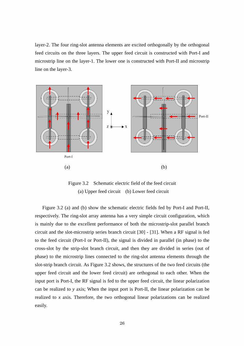
layer-2. The four ring-slot antenna elements are excited orthogonally by the orthogonal
feed circuits on the three layers. The upper feed circuit is constructed with Port-I and
microstrip line on the layer-1. The lower one is constructed with Port-II and microstrip
line on the layer-3.
(a) (b)
Figure 3.2 Schematic electric field of the feed circuit
(a) Upper feed circuit (b) Lower feed circuit
Figure 3.2 (a) and (b) show the schematic electric fields fed by Port-I and Port-II,
respectively. The ring-slot array antenna has a very simple circuit configuration, which
is mainly due to the excellent performance of both the microstrip-slot parallel branch
circuit and the slot-microstrip series branch circuit [30] - [31]. When a RF signal is fed
to the feed circuit (Port-I or Port-II), the signal is divided in parallel (in phase) to the
cross-slot by the strip-slot branch circuit, and then they are divided in series (out of
phase) to the microstrip lines connected to the ring-slot antenna elements through the
slot-strip branch circuit. As Figure 3.2 shows, the structures of the two feed circuits (the
upper feed circuit and the lower feed circuit) are orthogonal to each other. When the
input port is Port-I, the RF signal is fed to the upper feed circuit, the linear polarization
can be realized to y axis; When the input port is Port-II, the linear polarization can be
realized to x axis. Therefore, the two orthogonal linear polarizations can be realized
easily.

27
-50
-40
-30
-20
-10
0
S-pa
ram
ater
[dB
]
1098765
Frequency [GHz]
Simulated return loss of Port-I Simulated return loss of Port-II Simulated isolation between Port-I and Port-II
The simulator Ansoft HFSS is used for designing and analyzing the proposed
ring-slot array antenna shown in Figure 3.1. In the simulation, the relative dielectric
constant of substrate εr is 2.15 and the thickness is 0.8 mm. The design frequency is 7.5 GHz. The size of antenna ground plane is 60 mm × 60 mm. The RF signals are fed to
Port-I and Port-II microstrip lines with 2.4 mm width. The characteristic impedance of
the feed microstrip lines and the slot lines are 50 Ω and 102 Ω, respectively. The
characteristic impedance of microstrip lines connected to the ring-slot antennas is 83 Ω
for the impedance matching. The length and width of the ring-slot are 48 mm which is a
guided wave length λg at the design frequency of 7.5 GHz and 1.6 mm, respectively.
Figure 3.3 shows the S-parameters of the proposed ring-slot antenna array. The
isolation between two input ports is better than -30 dB, the return loss both Port-I and
Port-II are better than -10 dB in the frequency range of 6 GHz to 7.8 GHz, and the
relative bandwidth of the return loss for better than -10 dB is 26%.
Figure 3.3 Simulated return loss and isolation of the array antenna
By this result, the broad-band ring-slot array antenna for simultaneous use of
orthogonal linear polarizations is confirmed. The excellent isolation of two input ports
better than -30 dB is obtained mainly due to no electric interferes between the
microstrip-lines and the slot lines in the feed circuit. The broad impedance bandwidth

28
-40
-30
-20
-10
0
10
20
Dire
ctiv
ily [d
Bi]
-180 -120 -60 0 60 120 180
Angle [deg.]
E co E cross H co H cross
-40
-30
-20
-10
0
10
20
Dire
ctiv
ily [d
Bi]
-180 -120 -60 0 60 120 180
Angle [deg.]
E co E cross H co Hcross
and simple antenna structure are obtained mainly due to the orthogonal feed circuits
realized by the use of Both-Sided MIC technology.
(a)
(b)
Figure 3.4 Radiation pattern at 7.5 GHz
(a) Excited by Port-I
(b) Excited by Port-II

29
The far field of the 2×2 ring-slot antenna array is also simulated by HFSS. Figure 9
shows the radiation patterns of the proposed ring-slot antenna array. When the RF signal
is fed to Port-I, the directivity for linear polarization (y plane) of the proposed array
antenna is shown in Figure 3.4 (a). The gain in the boresight direction is 9.92 dBi at 7.5
GHz. The cross polarized radiation on both the E-plane and H-plane are better than -20
dBi. The excellent suppression is mainly due to the symmetrical and balanced
arrangement of feed circuits. When the RF signal is fed to Port-II, the directivity for
linear polarization (x plane) of the proposed array antenna is shown in Figure 3.4 (b).
The same polarization performance is obtained due to the symmetrical feed circuits.
As a result, the broad-band linear polarization ring-slot array antenna with simple
structure is theoretically confirmed.
3.3 Experimental Results and Discussion
The array antenna is fabricated on a Teflon Glass Fiber substrate with the relative
dielectric constant of εr = 2.15. The thickness of the structure is 0.8 mm. The photo of this fabricated antenna is shown in Figure 3.5. The antenna size is 60 mm×60 mm. The
Obverse side Reverse side
Figure 3.5 Photograph of the fabricated ring-slot array antenna

30
The anechoic chamber
Network Analyzer 8510C (Agilent)
Figure 3.6 Photograph of the experimental equipments

31
-50
-40
-30
-20
-10
0
S-pa
ram
ater
[dB
]
1098765
Frequency [GHz]
Measuerd return loss of Port-I Measured return loss of Port-II Measured isolation between Port-I and Port-II
antenna performance is measured through the experiment using an Agilent Network
Analyzer 8510C in an anechoic chamber. A linear polarization horn antenna is used to
measure the proposed antenna. The horn antenna is set at a distance of 2m from the
proposed antenna. The antenna is located on a turn table. The photos of the
experimental equipments are shown in Figure 3.6.
Figure 3.7 shows the S-parameters of the antenna. The isolation between two input
ports is better than -30 dB. The measured return loss of both the Port-I and the Port-II
are better than -10 dB in the frequency range over 6.5 GHz to 8.1 GHz. The broadband
performance is obtained in the measurement.
Figure 3.7 Measured return loss and isolation of the array antenna
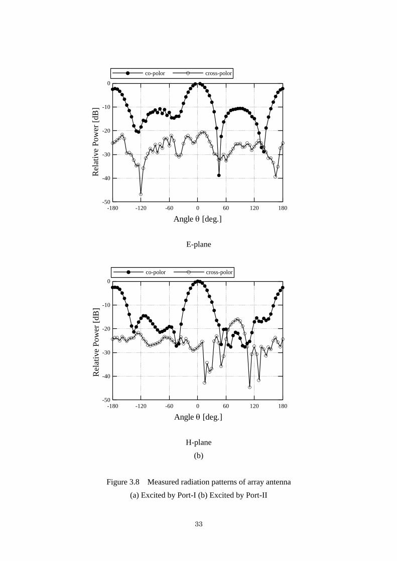
Figure 3.8 (a) shows the measured radiation pattern of the linear polarization (y
plane) where the feed port is Port-I. The cross polarized radiation on both the E-plane
and H-plane are better than -20 dBi. Figure 3.8 (b) shows the measure radiation pattern
of the linear polarization (x plane) where the feed port is Port-II. Comparing the
radiation pattern of the two orthogonal linear polarizations, almost same polarization
performance are obtained.

32
-50
-40
-30
-20
-10
0R
elat
ive
Pow
er [d
B]
-180 -120 -60 0 60 120 180
Angle θ [deg.]
co-polar cross-polor
-50
-40
-30
-20
-10
0
Rel
ativ
e Po
wer
[dB
]
-180 -120 -60 0 60 120 180
Angle θ [deg.]
co-polor cross-polor
E-plane
H-plane
(a)
33
-50
-40
-30
-20
-10
0
Rel
ativ
e Po
wer
[dB
]
-180 -120 -60 0 60 120 180
Angle θ [deg.]
co-polor cross-polor
-50
-40
-30
-20
-10
0
Rel
ativ
e Po
wer
[dB
]
-180 -120 -60 0 60 120 180
Angle θ [deg.]
co-polor cross-polor
E-plane
H-plane
(b)
Figure 3.8 Measured radiation patterns of array antenna
(a) Excited by Port-I (b) Excited by Port-II

34
The measured characteristics of the antenna are compared with the simulation date.
The measured results agree well with the simulated results.
As a result, the proposed array antenna can be achieved in a wide impedance
bandwidth. The good linear polarization performance can be achieved. The broad-band
linear polarization ring-slot array antenna for the orthogonal polarization simultaneous
use is successfully confirmed in the simulation and the measurement.
3.4 Conclusion
In this chapter, a novel broad-band linear polarization ring-slot array antenna is
described. The orthogonal linear polarizations can be realized simultaneously with good
polarization performance by using the proposed antenna. Because of the use of the
characteristics of the ring-slot antenna and the both-sided MIC technology, the excellent
performance such as broad-band, good isolation, and better cross polarization
suppression is obtained. In addition, the antenna structure is very simple, and the
antenna design is practically easy.
The proposed slot-ring array antenna is designed and achieved. The measured
results show that both the S-parameters and polarization performance of the antenna are
remarkably excellent. Therefore, the broad-band linear polarization ring-slot array
antenna is very suited for the wireless communication systems due to the advantages of
a most simple structure and the easier antenna design.

35
Chapter 4
Circularly Polarized Ring-Sot Array Antenna for Simultaneous Use of the
Orthogonal Polarizations
4.1 Introduction
As mentioned in previous chapter, the proposed ring-slot array antenna radiating
two orthogonal linear polarizations. However, there are other aspects that are equally
important and should be considered in a complete antenna design. These include the
design of feed, polarization diversity. In this chapter, the design consideration for
circular polarization ring-slot array antenna is presented. Figure 4.1 shows the technical
concept for circularly polarized ring-slot array antenna, where a π/2 hybrid circuit is integrated with the antenna. In this approach, the simultaneous use of the right-hand
circular polarization (RHCP) and the left-hand circular polarization (LHCP) can be
achieved.
Figure 4.1 Basic configuration of the proposed circularly polarized array antenna

36
In this chapter, a novel broad-band ring-slot array antenna for simultaneous use of
orthogonal polarizations is described. In this antenna, the broad-band performance is
obtained by integrating a 2×2 ring-slot array antenna that described in chapter 3, and a
broad-band π/2 hybrid circuit. The simultaneous use of the right-hand circular polarization (RHCP) and the left-hand circular polarization (LHCP) is achieved using
orthogonal feed circuits on three layers. The both-sided MIC technology is effectively
employed in forming this type of slot array antenna. Experimental results show that the
proposed antenna has good circular polarization characteristics for both the LHCP and
the RHCP. The measured impedance-bandwidth of return loss better than -10 dB is
about 47% both for the LHCP and the RHCP. The 3 dB axial ratio (AR) bandwidths are
25% (RHCP) and 29% (LHCP). The isolation between the two input ports is better than
-35 dB at center frequency of 7.5 GHz.
4.2 Circularly Polarized Ring-slot Array Antenna Using π/2
Hybrid Circuit
Antennas exhibiting circular polarization diversity and broad-band performance
have the advantages of frequency reuse for doubling the system capability and a high
degree of polarization control to optimize system performance. A number of antenna
architectures, offering circular polarization agility, have been proposed [32]-[34]. In
these antennas, circular polarization is obtained and the polarization diversity is
achieved by using pin-diodes embedded in the antenna. Due to the simple structure,
these antennas are attractive for wireless communications, being especially effective for
polarization diversity. However, one main disadvantage of these antennas is very narrow
bandwidth. Many other antennas are reported to obtain broad-band circular polarization.
In [35], a typical circular-ring slot antenna utilizing a strip-line hybrid coupler feed
network achieves good broad-band circular polarization performance. In [36], a
broad-band annular-slot antenna array with circular polarization has been reported. In
these papers, the circular polarization with broad-band performance has been discussed
so far. However, there is no report that investigates broad-band antennas with circular
polarization diversity.
Therefore, a ring-slot array antenna is designed to radiate two orthogonal circular
polarizations (RHCP/LHCP) with broad bandwidth. The structure of the proposed array

37
antenna is shown in Figure 4.2. The 2×2 ring-slot array and a π/2 hybrid circuit are
integrated in the proposed antenna. The π/2 hybrid circuit provides two equal input powers with ±90 degrees phase difference for the 2×2 ring-slot antenna array. The 2×2
ring-slot antenna array can provide simultaneous use of the orthogonal circular
polarizations with broad bandwidth. The proposed antenna is constructed with 2 layer
dielectric substrates, conductive 3 layers and two input port (Port-A and Port-B).
Figure 4.2 Structure of ring-slot array antenna (a) Top view
(b) Side view (A-A’) (c) Side view (B-B’)

38
5
4
3
2
1
0
AR
[dB
]
9.59.08.58.07.57.06.56.05.55.04.5
Frequency [GHz]
LHCP RHCP
In chapter 3, a novel linear polarization ring-slot array antenna with simple structure
is described. The array antenna shown in Figure 3.1 can radiate two orthogonal linear
polarizations. If two RF signals are fed to the two port of the array antenna respectively
with ±90 degrees phase difference, the circular polarization can be realized. In the
case of the two RF signals which have +90 deg. phase difference are fed to the two
input ports (Port-I and Port-II), the RHCP can be realized. When the phase difference of
the two RF signals is -90 deg, the LHCP can be realized. Therefore the proposed slot
array antenna can radiate orthogonal circular polarizations simultaneously.
The circular polarization performance of the array antenna is simulated by the HFSS.
The simulation model is shown in Figure 3.1. In the simulation, the phase difference
between the two RF signals (Port-I vs. Port-II) is +90 degrees and -90 degrees to realize
the RHCP and the LHCP, respectively. The design frequency is 7.5 GHz.
Figure 4.3 shows the simulated axial ratio (AR) of the 2×2 ring-slot array antenna
for both the RHCP and the LHCP. As a result, the axial ratio (AR < 3 dB) relative
bandwidth of the RHCP and the LHCP are 51% and 50%, respectively. The broad
bandwidth of axial ratio is confirmed mainly due to the orthogonal feed circuits realized
by the use of Both-Sided MIC technology.
Figure 4.3 Simulated axial ratio (AR) of the array antenna
The far field of the 2×2 ring-slot antenna array is also simulated by HFSS. Figure
4.4 shows the radiation patterns of the proposed ring-slot antenna array. The RHCP and
39
-40
-35
-30
-25
-20
-15
-10
-5
0D
irect
ivity
[dB
]
-180 -120 -60 0 60 120 180
Angle [deg.]
RHCP LHCP
-40
-35
-30
-25
-20
-15
-10
-5
0
Dire
ctiv
ity [d
B]
-180 -120 -60 0 60 120 180
Angle [deg.]
LHCP RHCP
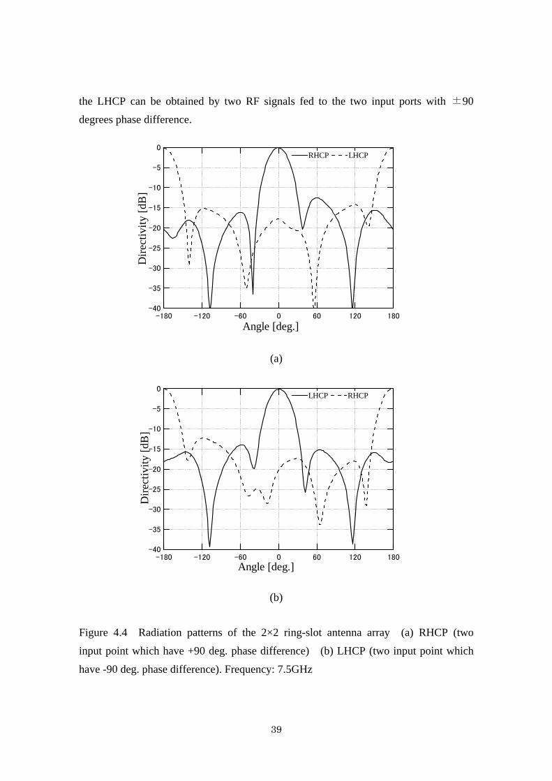
the LHCP can be obtained by two RF signals fed to the two input ports with ±90
degrees phase difference.
(a)
(b)
Figure 4.4 Radiation patterns of the 2×2 ring-slot antenna array (a) RHCP (two
input point which have +90 deg. phase difference) (b) LHCP (two input point which
have -90 deg. phase difference). Frequency: 7.5GHz
40
According to these results and the S-parameters of the array antenna mentioned in
section 3.2, the broadband circular polarization slot antenna array for orthogonal
polarization simultaneous use is theoretically confirmed.
4.3 Broad-Band Microstrip π/2 Hybrid Circuit
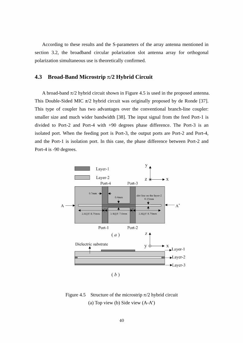
A broad-band π/2 hybrid circuit shown in Figure 4.5 is used in the proposed antenna. This Double-Sided MIC π/2 hybrid circuit was originally proposed by de Ronde [37].
This type of coupler has two advantages over the conventional branch-line coupler:
smaller size and much wider bandwidth [38]. The input signal from the feed Port-1 is
divided to Port-2 and Port-4 with +90 degrees phase difference. The Port-3 is an
isolated port. When the feeding port is Port-3, the output ports are Port-2 and Port-4,
and the Port-1 is isolation port. In this case, the phase difference between Port-2 and
Port-4 is -90 degrees.
Figure 4.5 Structure of the microstrip π/2 hybrid circuit (a) Top view (b) Side view (A-A’)

41
-60
-50
-40
-30
-20
-10
0
S-pa
ram
eter
[dB
]
1098765
Frequency [GHz]
S11
S21 S41
S31
-180
-120
-60
0
60
120
180
Phas
e [d
eg.]
1098765
Frequency [GHz]
S21 S41
Figure 4.6 shows the simulated S-parameters of the π/2 hybrid circuit. In this case, the RF signal is fed to Port-I. The insertion loss is less than 1 dB in the frequency range
of 6 GHz to 9 GHz. The isolation and the return loss are better than -20 dB in the same
band. Figure 4.7 shows the frequency characteristics of the phase. The phase difference
of +90 deg. is obtained in the frequency range of 6 GHz to 9 GHz.
Figure 4.6 Simulated S-parameter of the circuit
Figure 4.7 Simulated phase difference of the circuit

42
As a result, the broad band performance and π/2 phase shift behavior can be achieved in this circuit.
4.4 Experiment
According to the better performance described above, the broad-band circular
polarization ring-slot array antenna is fabricated on a Teflon Glass Fiber substrate with
the relative dielectric constant εr of 2.15. The thickness of the substrate is 0.8 mm. The fabricated ring-slot array antenna for the experiment is shown in Figure 4.8. The size of
the antenna ground plane is 75mm×110mm. The π/2 hybrid circuit and the ring-slot array are integrated on three layer substrates. The electric length of two feed circuits are
the same to provide the excitation of antenna orthogonally, where
L1+L2=L3+L4+L5+L6 = 2.8 λg as shown in Figure 4.1. By feeding the RF signals to the input ports of proposed antenna (Port-A and Point-B), the RHCP and LHCP can be
obtained simultaneously.
(a)

43
(b)
Figure 4.8 Photos of the proposed ring-slot array antenna
(a) Top view (b) Bottom View
The performance is measured through the experiment using an Agilent Network
Analyzer 8510C in an anechoic chamber. A linear polarization horn antenna is used to
measure the proposed antenna. The horn antenna is set at a distance of 2m from the
proposed antenna. The proposed antenna is located on a turn table.
Figure 4.9 shows the measured return loss of the proposed ring-slot array antenna.
The return loss impedance bandwidth of better than -10 dB is about 47% (5.37 GHz -
8.76 GHz). The measured -10 dB return loss bandwidth of the array antenna including
the π/2 hybrid is better than the simulated -10 dB return loss bandwidth of the only
antenna array as shown in Figure 3.3. The reason is that, the broad band π/2 hybrid circuit can improve the return loss performance of the proposed antenna. And from the
result shown in Figure 4.10, a good isolation performance better than -30dB is obtained
in the frequency range of 6.3GHz to 8GHz.

44
-40
-30
-20
-10
0
Ret
urn
loss
[dB
]
1098765
Frequency [GHz]
S AA S BB
-50
-40
-30
-20
-10
0
Isol
atio
n [d
B]
1098765
Frequency [GHz]
Figure 4.9 Measured return loss of the proposed array antenna
Figure 4.10 Measure isolation of the two proposed array antenna input ports
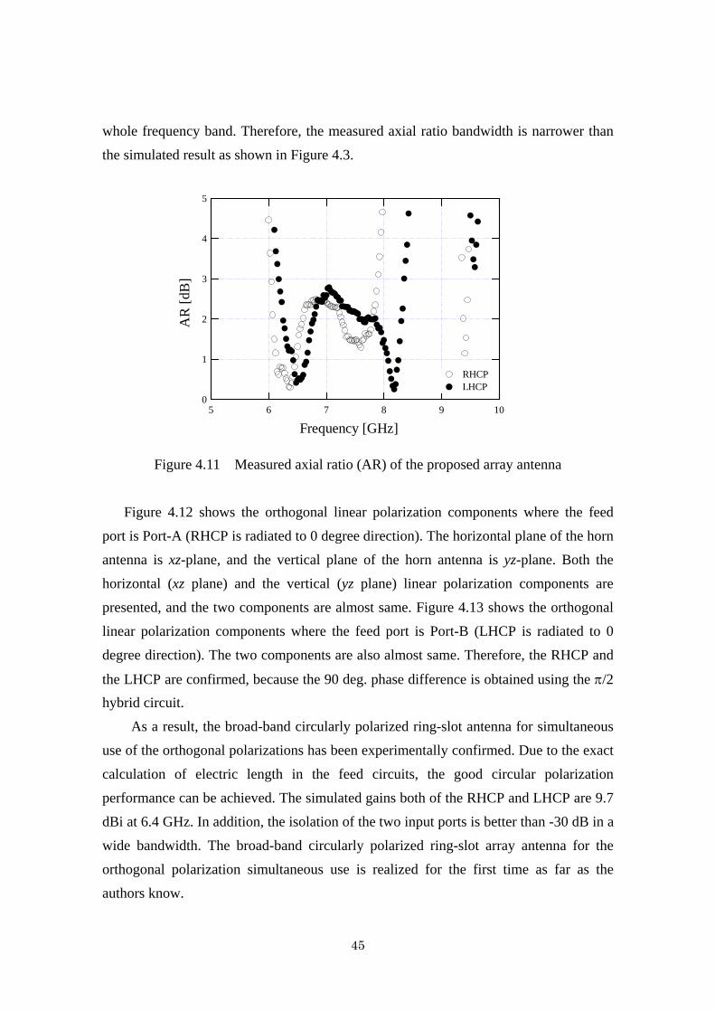
Figure 4.11 shows the measured axial ratio (AR). The 3 dB axial ratio bandwidth for
the RHCP and the LHCP are 25% and 29% with respect to 7.25 GHz, respectively. In
the experiment, the 90 degrees phase difference and the amplitude of the two linear
polarization components is changed with the frequency changing due to the frequency
characteristics of the π/2 hybrid circuit. In the simulation, the 90 degrees phase difference and the same amplitude of two linear polarization components are set up in
45
5
4
3
2
1
0
AR
[dB
]
1098765
Frequency [GHz]
RHCP LHCP
whole frequency band. Therefore, the measured axial ratio bandwidth is narrower than
the simulated result as shown in Figure 4.3.
Figure 4.11 Measured axial ratio (AR) of the proposed array antenna
Figure 4.12 shows the orthogonal linear polarization components where the feed
port is Port-A (RHCP is radiated to 0 degree direction). The horizontal plane of the horn
antenna is xz-plane, and the vertical plane of the horn antenna is yz-plane. Both the
horizontal (xz plane) and the vertical (yz plane) linear polarization components are
presented, and the two components are almost same. Figure 4.13 shows the orthogonal
linear polarization components where the feed port is Port-B (LHCP is radiated to 0
degree direction). The two components are also almost same. Therefore, the RHCP and
the LHCP are confirmed, because the 90 deg. phase difference is obtained using the π/2 hybrid circuit.
As a result, the broad-band circularly polarized ring-slot antenna for simultaneous
use of the orthogonal polarizations has been experimentally confirmed. Due to the exact
calculation of electric length in the feed circuits, the good circular polarization
performance can be achieved. The simulated gains both of the RHCP and LHCP are 9.7
dBi at 6.4 GHz. In addition, the isolation of the two input ports is better than -30 dB in a
wide bandwidth. The broad-band circularly polarized ring-slot array antenna for the
orthogonal polarization simultaneous use is realized for the first time as far as the
authors know.

46
-40
-30
-20
-10
0
Rel
ativ
e Po
wer
[dB
]
-180 -120 -60 0 60 120 180
Ang. [deg]
xz yz
-40
-30
-20
-10
0
Rel
ativ
e Po
wer
[dB
]
-180 -120 -60 0 60 120 180
Ang.[deg]
xz yz
Figure 4.12 Radiation pattern of the proposed array antenna (Port-A)
Frequency : 6.4 GHz
Figure 4.13 Radiation pattern of the proposed array antenna (Port-B)
Frequency : 6.4 GHz

47
4.5 Conclusion
In this chapter, a broad-band circular polarization annular ring-slot array antenna for
simultaneous use of the orthogonal polarizations is proposed. The proposed antenna can
provide wide impedance bandwidth of 47%. The 3 dB axial ratio bandwidths are wider
than 25% (RHCP) and 29% (LHCP). The Both-Sided MIC technology is effectively
applied to configure the proposed slot array antenna.
Excellent performance such as broad-band, good isolation and simultaneous use of
the orthogonal circular polarizations is obtained. The proposed ring-slot array antenna
can find promising application such as radar and polarimetric sensors. Moreover, by
integrating a switch circuit in the proposed antenna, an orthogonal circular polarizations
switchable slot array antenna can be realized easily.
48
Chapter 5
Linear Polarization Switchable Ring-Slot Array Antenna Using SPDT Circuit
5.1 Introduction
A broad-band ring-slot array antenna which can radiate linear polarizations and the
circular polarizations is described in last two chapters. However, the polarization
switching function can not be obtained by using the array antennas that mentioned in
last two chapters. Various antenna architectures, offering polarization agility, that is,
realizing polarization switching function, have been proposed [39] – [41]. In these
antennas, polarization diversity is achieved by using PIN diodes or varactor diodes
embedded in the antennas. In [39], the polarization angle is controlled by switching the
resonant mode of the patch antenna, where the switching of resonant modes is achieved
by adjustment of the conditions of the PIN diodes. These antennas are attractive for
wireless communications, being especially effective for polarization diversity due to
their simple structures. Moreover, a ring-slot antenna that allows polarization diversity
has been reported [42]. The characteristics of a single element antenna with
polarization diversity have been discussed in these papers; however, the investigation of
the array antenna with polarization diversity has not been involved. Recently, a slot-ring
array antenna with polarization switchable function is proposed in a paper [43], where a
four elements ring-slot array antenna was presented whose orthogonal polarization can
be switched. The orthogonal polarization is switched by using sixteen switching diodes
embedded in the slot-ring antenna elements. However, this array antenna requires many
diodes for antenna fabrication.
Therefore, by using a Single Pole Double Throw (SPDT) switch circuit, a novel
linear polarization ring-slot array antenna is proposed and described in this chapter. The
49
linear polarization switchable function is achieved using the SPDT switch circuit. Two
Schottky barrier diodes are mounted on a slot ring of the SPDT switch circuit. As the
orthogonal linear polarization switching depends on the diode ON/OFF conditions, the
polarization angle is easily controlled by the polarity of the bias voltage. The excellent
design flexibility of the Both-Sided MIC technology is effectively employed in forming
this type of antenna. Experimental results show that the proposed antenna has good
polarization characteristics for the two orthogonal linear polarizations. The radiation
performances of two orthogonal polarizations are almost the same. Consequently, a
linear polarization switchable ring-slot array antenna is successfully verified.
5.2 Design of Ring-Slot Array Antenna For Linear Polarization
Switching
A linear polarization switchable ring-slot array antenna is mentioned in section 5.1;
the antenna design is performed on the HFSS and ADS as well.
5.2.1 Antenna Configuration
The proposed linear polarization switchable ring-slot array antenna is shown in
Figure 5.1. The antenna consists of the ring-slot array antenna that mentioned in chapter
3 and the SPDT switch circuit. The ring-slot array can radiate two orthogonal linear
polarizations. The SPDT circuit switches two feed circuits of RF signal to the ring-slot
array antenna. The array antenna is constructed with 2 layer dielectric substrates and 3
conductive layers.
The configuration and basic operation of the ring-slot array is explained chapter 3. A
better impedance performance and linear polarization performance is obtained by the
proposed ring-slot array. By fed a RF signal to Port-I or Port-II (Figure 3.1), the two
orthogonal linear polarizations can be realized easily.
The linear polarization switchable array antenna that described in this chapter can
have the polarization switching function due to the using of a novel three layers SPDT
switch circuit. And the basic operation and the configuration of the SPDT switch circuit
will be described in detail in the next section.

50
(a)
(b)
(c)
Figure 5.1 Linear polarization switchable ring-slot array antenna
(a): Top view (b): Side view A-A’ (c): Side view B-B’
51
5.2.2 SPDT Switch Circuit
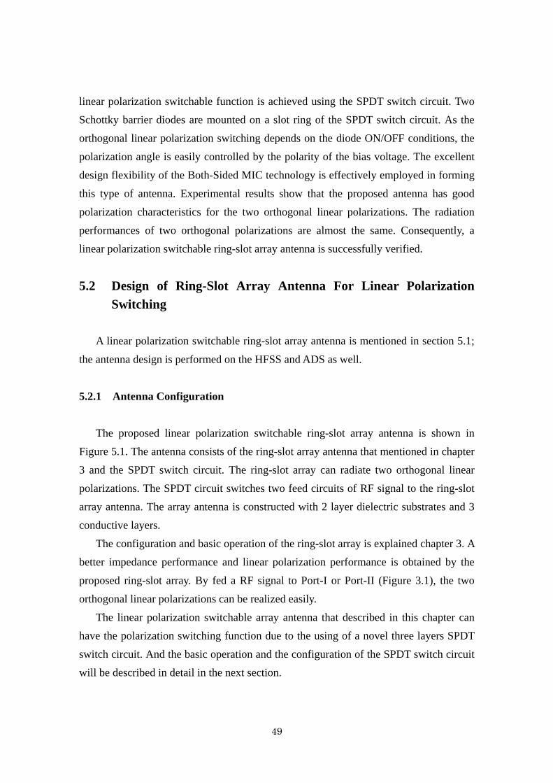
Figure 5.2 shows the configuration of the proposed SPDT switch circuit. The SPDT
circuit consists of a two wavelength ring-slot on layer-2, an input microstrip line and
output microstrip lines connected to Port-2 on layer-1 and Port-3 on layer-3, and two
Schottky barrier diodes mounted on the ring-slot. The switching bias is supplied to the
switching diodes through the conductor wire connected to the coplanar waveguide. Two
1/2 wavelength open stub microstrip lines on layer-1 and layer-3 are used in the switch
circuit to isolate the two output ports. As shown in Figure 5.2, two Schottky barrier
diodes are loaded on the ring-slot at ±45 degrees with respect to the input microstrip
line (Port-1).
Figure 5.2 Configuration of the SPDT switch circuit
(a): Top view (b): Side view A-A’
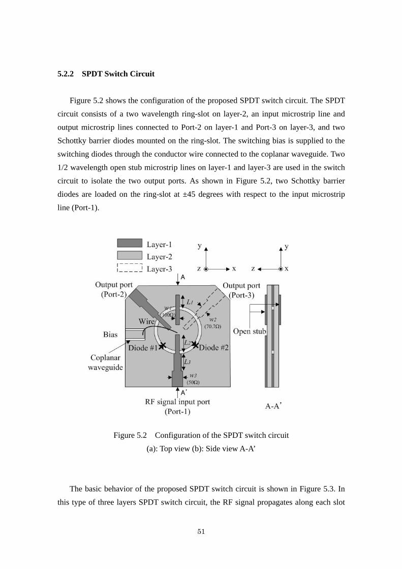
The basic behavior of the proposed SPDT switch circuit is shown in Figure 5.3. In
this type of three layers SPDT switch circuit, the RF signal propagates along each slot
52
line according to the polarity of the switching bias voltage. When a positive voltage is
applied to the inner conductor of ring-slot, the diode #2 is ON, and the diode #1 is OFF.
In this condition, the switch circuit transmits the RF signal to the Port-2 on layer-1 as
shown in Figure 5.3 (a). When the polarity of the bias voltage applied to the diode is
reversed, the switch circuit transmits the RF signal to the Port-3 on layer-3 as shown in
Figure 5.3 (b). Therefore, the output port of RF signal can be switched easily.
(a) (b)
Figure 5.3 Schematic electric field of the SPDT switch circuit
(a): Diode #1 OFF, Diode #2 ON (b): Diode #1 ON, Diode #2 OFF
The characteristics of the SPDT switch circuit are designed and fabricated. The
circuit is fabricated on a Teflon Glass Fiber substrate with the relative dielectric constant
εr of 2.15. The thickness of the substrate is 0.8 mm. The optimized parameters of the SPDT switch circuit dimensions are as follows: L 1 = L 2 = 0.25λg = 7.6 mm, L 3 =
0.25λg = 7.46 mm, w1 = 0.7 mm, w2 = 1.4 mm, w3 = 2.4 mm; the characteristic
impedance of the feed microstrip lines (Port-1, 2 and 3) is 50 Ω. The characteristic
impedance of microstrip lines connected to the ring-slot is 70.7 Ω for the impedance
matching. The length of the conductor wire is 1.5 cm. The length and width of the
ring-slot are 68.44 mm and 0.2 mm, respectively. Two Schottky barrier diodes (Metelics
MSS30, 154-B10B) are used in the SPDT switch circuit.
53
-50
-40
-30
-20
-10
0
Ret
urn-
loss
[dB
]
1098765
Frequency [GHz]
Simulated: S11Measured: S11 (positive bias ) S11 (negative bias)
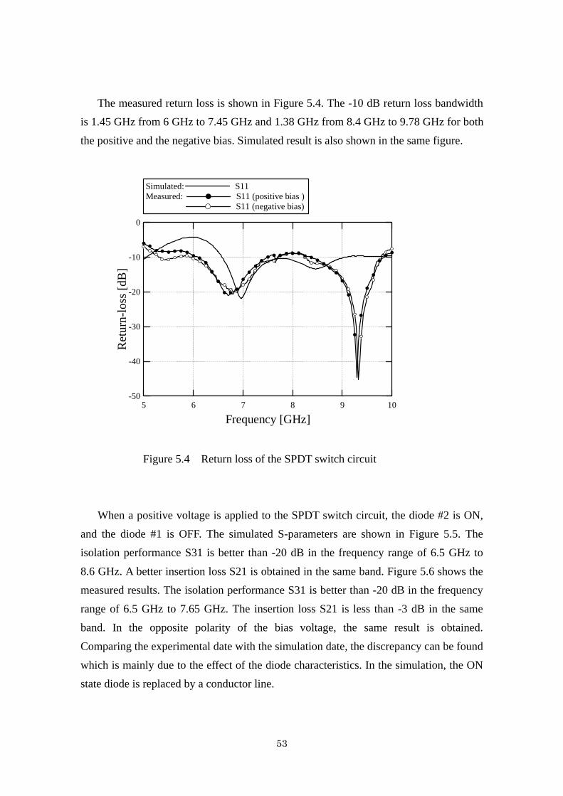
The measured return loss is shown in Figure 5.4. The -10 dB return loss bandwidth
is 1.45 GHz from 6 GHz to 7.45 GHz and 1.38 GHz from 8.4 GHz to 9.78 GHz for both
the positive and the negative bias. Simulated result is also shown in the same figure.
Figure 5.4 Return loss of the SPDT switch circuit
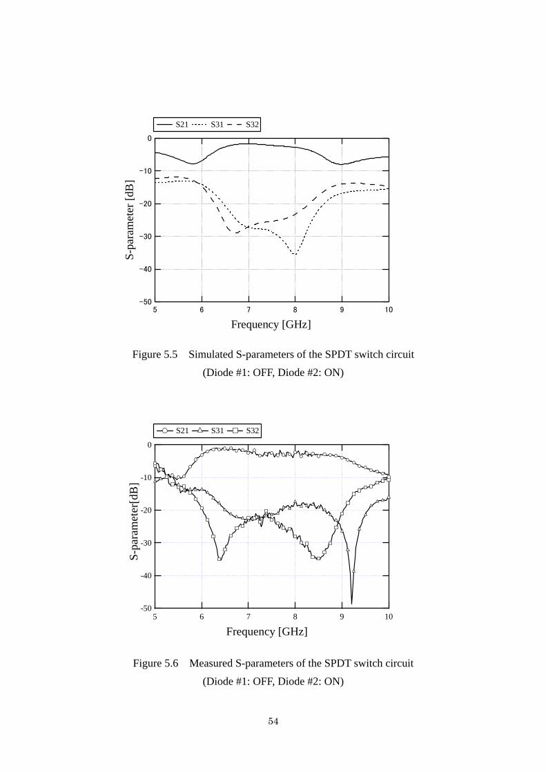
When a positive voltage is applied to the SPDT switch circuit, the diode #2 is ON,
and the diode #1 is OFF. The simulated S-parameters are shown in Figure 5.5. The
isolation performance S31 is better than -20 dB in the frequency range of 6.5 GHz to
8.6 GHz. A better insertion loss S21 is obtained in the same band. Figure 5.6 shows the
measured results. The isolation performance S31 is better than -20 dB in the frequency
range of 6.5 GHz to 7.65 GHz. The insertion loss S21 is less than -3 dB in the same
band. In the opposite polarity of the bias voltage, the same result is obtained.
Comparing the experimental date with the simulation date, the discrepancy can be found
which is mainly due to the effect of the diode characteristics. In the simulation, the ON
state diode is replaced by a conductor line.
54
-50
-40
-30
-20
-10
0S-
para
met
er [d
B]
1098765
Frequency [GHz]
S21 S31 S32
-50
-40
-30
-20
-10
0
S-pa
ram
eter
[dB
]
1098765
Frequency [GHz]
S21 S31 S32
Figure 5.5 Simulated S-parameters of the SPDT switch circuit
(Diode #1: OFF, Diode #2: ON)
Figure 5.6 Measured S-parameters of the SPDT switch circuit
(Diode #1: OFF, Diode #2: ON)

55
According to these results, a wide band SPDT switch circuit is achieved. The better
circuit performance can be realized by matching the impedances of microstrip lines and
ring-slot on the SPDT switch circuit further more.
As a result, the basic behavior of the SPDT switch circuit is confirmed theoretically
and experimentally. Moreover, the orthogonal linear polarization switchable ring-slot
array antenna integrating the 4 elements ring-slot array and the SPDT switch circuit can
be simply achieved in the same substrate.
5.3 Experimental Results and Discussion
The integrated orthogonal linear polarization switchable array antenna of the
ring-slot array and the SPDT switch circuit is fabricated and measured. The photos of
the fabricated antenna are shown in Figure 5.7. The size of the ground plane is 70 mm ×
120 mm.
(a) (b)
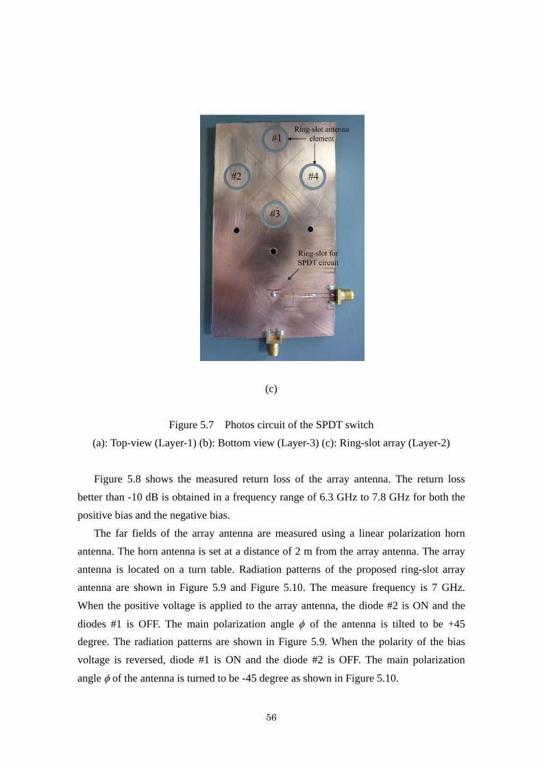
56
(c)
Figure 5.7 Photos circuit of the SPDT switch
(a): Top-view (Layer-1) (b): Bottom view (Layer-3) (c): Ring-slot array (Layer-2)
Figure 5.8 shows the measured return loss of the array antenna. The return loss
better than -10 dB is obtained in a frequency range of 6.3 GHz to 7.8 GHz for both the
positive bias and the negative bias.
The far fields of the array antenna are measured using a linear polarization horn
antenna. The horn antenna is set at a distance of 2 m from the array antenna. The array
antenna is located on a turn table. Radiation patterns of the proposed ring-slot array
antenna are shown in Figure 5.9 and Figure 5.10. The measure frequency is 7 GHz.
When the positive voltage is applied to the array antenna, the diode #2 is ON and the
diodes #1 is OFF. The main polarization angle φ of the antenna is tilted to be +45 degree. The radiation patterns are shown in Figure 5.9. When the polarity of the bias
voltage is reversed, diode #1 is ON and the diode #2 is OFF. The main polarization
angle φ of the antenna is turned to be -45 degree as shown in Figure 5.10.

57
-30
-25
-20
-15
-10
-5
0
Ret
urn
Loss
[dB
]
1098765
Frequency [GHz]
positive voltage negative viltage
-30
-25
-20
-15
-10
-5
0
Rel
ativ
e Po
wer
[dB
]
-180 -120 -60 0 60 120 180
Angle θ [deg.]
co-polor cross-polor
Figure 5.8 Measured return loss of the array antenna
E-plane

58
-30
-25
-20
-15
-10
-5
0R
elat
ive
Pow
er [d
B]
-180 -120 -60 0 60 120 180
Angle θ [deg.]
co- polor cross-polor
-30
-25
-20
-15
-10
-5
0
Rel
ativ
e Po
wer
[dB
]
-180 -120 -60 0 60 120 180
Angle θ [deg.]
co-polor cross-polor
H-plane
Figure 5.9 Measured radiation pattern of the polarization switchable array antenna at 7
GHz, φ = +45 degree, Diode #2 is ON
E-plane

59
-30
-25
-20
-15
-10
-5
0R
elat
ive
Pow
er [d
B]
-180 -120 -60 0 60 120 180
Angle θ [deg.]
co-polor cross polor
H-plane
Figure 5.10 Measured radiation pattern of the polarization switchable array antenna at
7 GHz, φ = −45 degree, Diode #1 is ON
The radiation patterns of the two orthogonal linear polarizations are almost same. In
an addition, the cross polarization level is about -20 dB at the bore-sight for both φ =
+45 degree linear polarization and φ = -45 degree linear polarization. The better cross polarization suppression of the array antenna is obtained because of the
complementarity effect of the mirror symmetry antenna structure and the good isolation
performance of the SPDT switch circuit.
The good performance of the two orthogonal linear polarizations is achieved, and
the polarization switching function is also realized by using the array antenna.
Consequently, the orthogonal linear polarization switchable ring-slot array antenna is
experimentally verified.
5.3 Conclusion
In this chapter, a novel linear polarization switchable ring-slot array antenna is
described, and the characteristics of the antenna are experimentally discussed. The

60
antenna can provide the switching function between the polarization angle of φ = +45
degree and φ = -45 degree. The Both-Sided MIC technology is effectively applied to form the array antenna. By the use of combination effect of a microstrip-slot parallel
power divider and a slot-microstrip series power divider, very simple circuit
configuration and good polarization performance can be achieved. The -10 dB return
loss bandwidth is obtained over 6.3 GHz to 7.8 GHz frequency range.
Extending this array antenna structure, sixteen elements array or thirty-two elements
ring-slot array antenna with linear polarization switching function can be easily realized
as well. The proposed slot array antenna can find promising applications such as various
radars and polarmetric sensors. Moreover, much wider applications can be found if a
reflector is added for a directional radiation pattern. Therefore, the proposed array
antenna is practically attractive for advanced wireless communication systems and the
other applications.
61
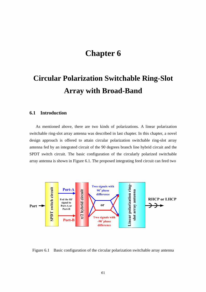
Chapter 6
Circular Polarization Switchable Ring-Slot
Array with Broad-Band
6.1 Introduction
As mentioned above, there are two kinds of polarizations. A linear polarization
switchable ring-slot array antenna was described in last chapter. In this chapter, a novel
design approach is offered to attain circular polarization switchable ring-slot array
antenna fed by an integrated circuit of the 90 degrees branch line hybrid circuit and the
SPDT switch circuit. The basic configuration of the circularly polarized switchable
array antenna is shown in Figure 6.1. The proposed integrating feed circuit can feed two
Figure 6.1 Basic configuration of the circular polarization switchable array antenna
62
RF signals with ±90 degrees and same amplitude to the ring-slot array. Moreover, the
90 degrees phase difference and the -90 degrees phase difference of the two feed RF
signals can be switched by the feed circuit. The excellent circular polarization
characteristics can be obtained by the ring-slot array. Therefore, a circular polarization
switchable ring-slot array antenna can be realized by integrating the ring-slot array, 90
degrees branch line hybrid circuit and SPDT switch circuit, and the proposed array
antenna is described in this chapter.
6.2 Principle of Proposed Ring-Slot Array Antenna
A circular polarization switchable ring-slot array antenna is mentioned in section 6.1.
The antenna principle is described in this chapter, and the antenna design is performed
on the HFSS and ADS as well.
6.2.1 Antenna design
The structure of the circular polarization switchable ring-slot array antenna is shown
in Figure 6.2. The antenna consist a ring-slot array, a 90 degrees branch line hybrid
circuit and a SPDT switch circuit. The array antenna is constructed with 2 layer
dielectric substrates and 3 conductive layers. The ring-slot array that mentioned in
chapter 3 is utilized to form this proposed antenna. The impedance performance and
circular polarization characteristics of the ring-slot array are described in chapter 3 and
section 2, chapter 4. The utilized ring-slot array can radiate the circular polarization
with good polarization performance in a wide frequency bandwidth. A conventional 90
degrees branch line hybrid circuit is used in the proposed array antenna. This branch
line hybrid circuit can provide the ring-slot array two RF signals with ±90 degrees
phases difference and same amplitude. The polarization switchable function can be
obtained by the use of a SPDT switch circuit.
A three layers SPDT switch circuit was described in section 5.2.2. This type of
SPDT switch circuit can switch the RF signals with excellent circuit performance in a
wide frequency bandwidth. In this chapter, in order to integrate the SPDT switch circuit
and branch line hybrid circuit in same structure, the design of the SPDT switch circuit
has a minor change. The used SPDT switch circuit in this chapter is constructed with 1

63
layer dielectric substrates with 2 conductive layers. The changed SPDT switch circuit is
remarkable suited for composing the proposed circular polarization switchable ring-slot
array antenna, and is described in next section in detail.
Figure 6.2 Structure of the circular polarization switchable ring-slot array antenna

64
The configuration and basic operation of the integrated feed circuit is explained in
next section.
6.2.3 Microstrip Branch Line Hybrid Circuit with SPDT Switch Circuit
The structure of the feed circuit is shown in Figure 6.3. The feed circuit consist a
conventional microstrip Branch line hybrid circuit and a SPDT switch circuit. In this
feed circuit, the SPDT switch circuit is designed with 1 layer dielectric substrates and 2
conductive layers.
Figure 6.3 Structure of the feed circuit
The SPDT circuit consists of a two wavelength ring-slot on layer-2, microstrip lines
on layer-1, and two Schottky barrier diodes mounted on the ring-slot. The switching
bias is supplied to the switching diodes through the conductor wire connected to the
coplanar waveguide. A 1/2 wavelength open stub microstrip lines on layer-1 is used in
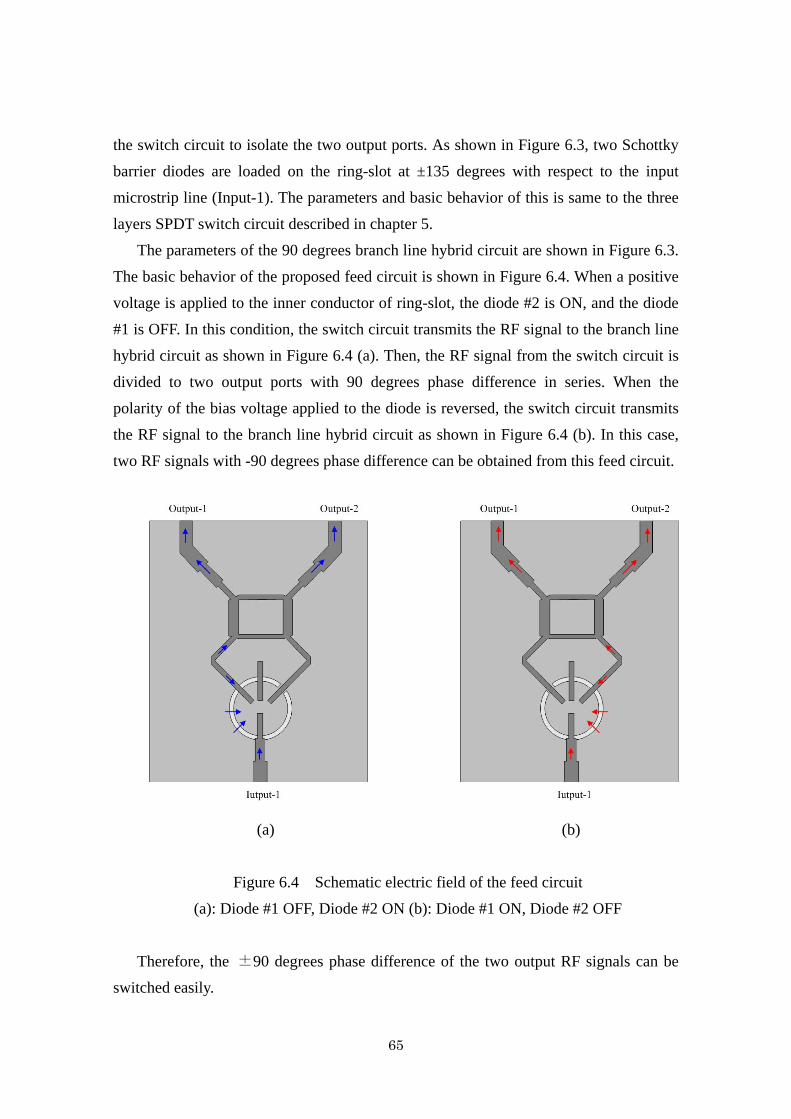
65
the switch circuit to isolate the two output ports. As shown in Figure 6.3, two Schottky
barrier diodes are loaded on the ring-slot at ±135 degrees with respect to the input
microstrip line (Input-1). The parameters and basic behavior of this is same to the three
layers SPDT switch circuit described in chapter 5.
The parameters of the 90 degrees branch line hybrid circuit are shown in Figure 6.3.
The basic behavior of the proposed feed circuit is shown in Figure 6.4. When a positive
voltage is applied to the inner conductor of ring-slot, the diode #2 is ON, and the diode
#1 is OFF. In this condition, the switch circuit transmits the RF signal to the branch line
hybrid circuit as shown in Figure 6.4 (a). Then, the RF signal from the switch circuit is
divided to two output ports with 90 degrees phase difference in series. When the
polarity of the bias voltage applied to the diode is reversed, the switch circuit transmits
the RF signal to the branch line hybrid circuit as shown in Figure 6.4 (b). In this case,
two RF signals with -90 degrees phase difference can be obtained from this feed circuit.
(a) (b)
Figure 6.4 Schematic electric field of the feed circuit
(a): Diode #1 OFF, Diode #2 ON (b): Diode #1 ON, Diode #2 OFF
Therefore, the ±90 degrees phase difference of the two output RF signals can be
switched easily.

66
In order to analysis the performance of the integrated feed circuit. The SPDT switch
circuit and the 90 degrees branch line hybrid circuit are simulated by ADS, respectively.
Figure 6.5 S-parameter of the 90 degrees branch line hybrid circuit
Figure 6.6 Phase difference of the branch line hybrid circuit
Figure 6.5 shows the S-parameters of the branch line hybrid circuit. The design
frequency of the branch line hybrid circuit is 7.5 GHz. The simulation model is shown
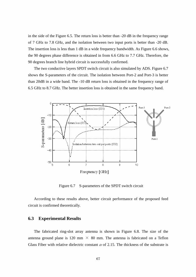
67
in the side of the Figure 6.5. The return loss is better than -20 dB in the frequency range
of 7 GHz to 7.8 GHz, and the isolation between two input ports is better than -20 dB.
The insertion loss is less than 1 dB in a wide frequency bandwidth. As Figure 6.6 shows,
the 90 degrees phase difference is obtained in from 6.6 GHz to 7.7 GHz. Therefore, the
90 degrees branch line hybrid circuit is successfully confirmed.
The two conductive layers SPDT switch circuit is also simulated by ADS. Figure 6.7
shows the S-parameters of the circuit. The isolation between Port-2 and Port-3 is better
than 20dB in a wide band. The -10 dB return loss is obtained in the frequency range of
6.5 GHz to 8.7 GHz. The better insertion loss is obtained in the same frequency band.
Figure 6.7 S-parameters of the SPDT switch circuit
According to these results above, better circuit performance of the proposed feed
circuit is confirmed theoretically.
6.3 Experimental Results
The fabricated ring-slot array antenna is shown in Figure 6.8. The size of the
antenna ground plane is 120 mm × 80 mm. The antenna is fabricated on a Teflon
Glass Fiber with relative dielectric constant εr of 2.15. The thickness of the substrate is
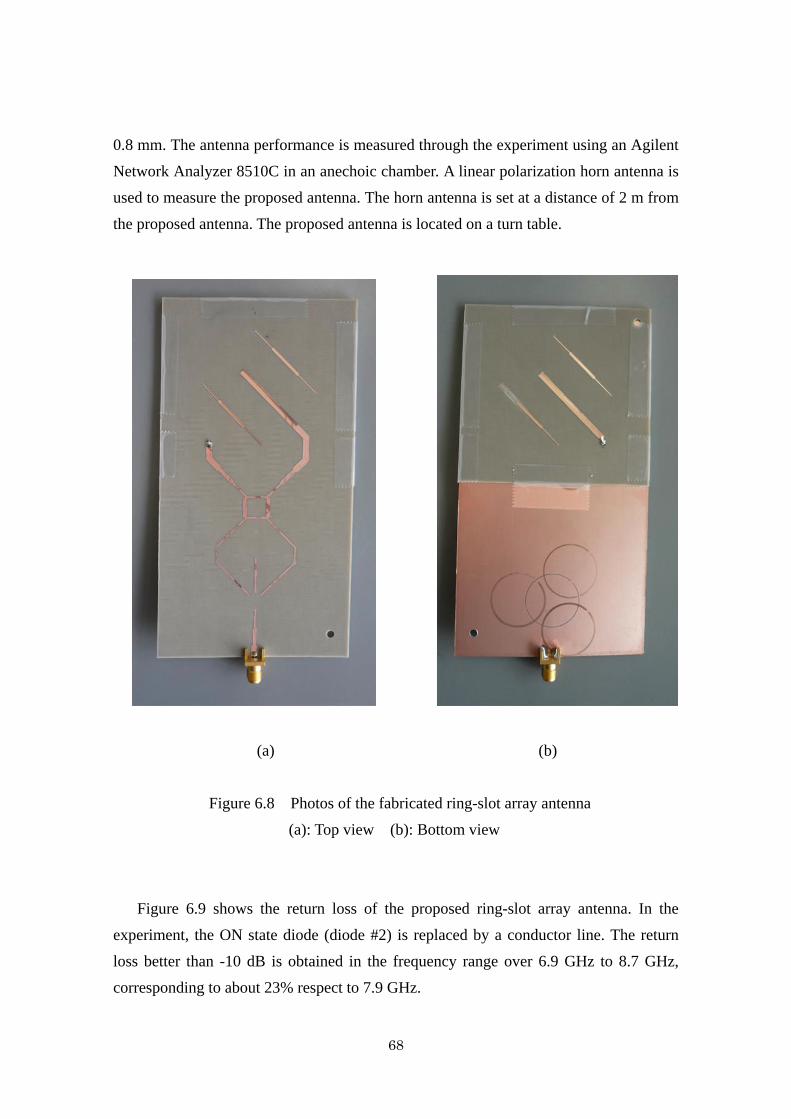
68
0.8 mm. The antenna performance is measured through the experiment using an Agilent
Network Analyzer 8510C in an anechoic chamber. A linear polarization horn antenna is
used to measure the proposed antenna. The horn antenna is set at a distance of 2 m from
the proposed antenna. The proposed antenna is located on a turn table.
(a) (b)
Figure 6.8 Photos of the fabricated ring-slot array antenna
(a): Top view (b): Bottom view
Figure 6.9 shows the return loss of the proposed ring-slot array antenna. In the
experiment, the ON state diode (diode #2) is replaced by a conductor line. The return
loss better than -10 dB is obtained in the frequency range over 6.9 GHz to 8.7 GHz,
corresponding to about 23% respect to 7.9 GHz.
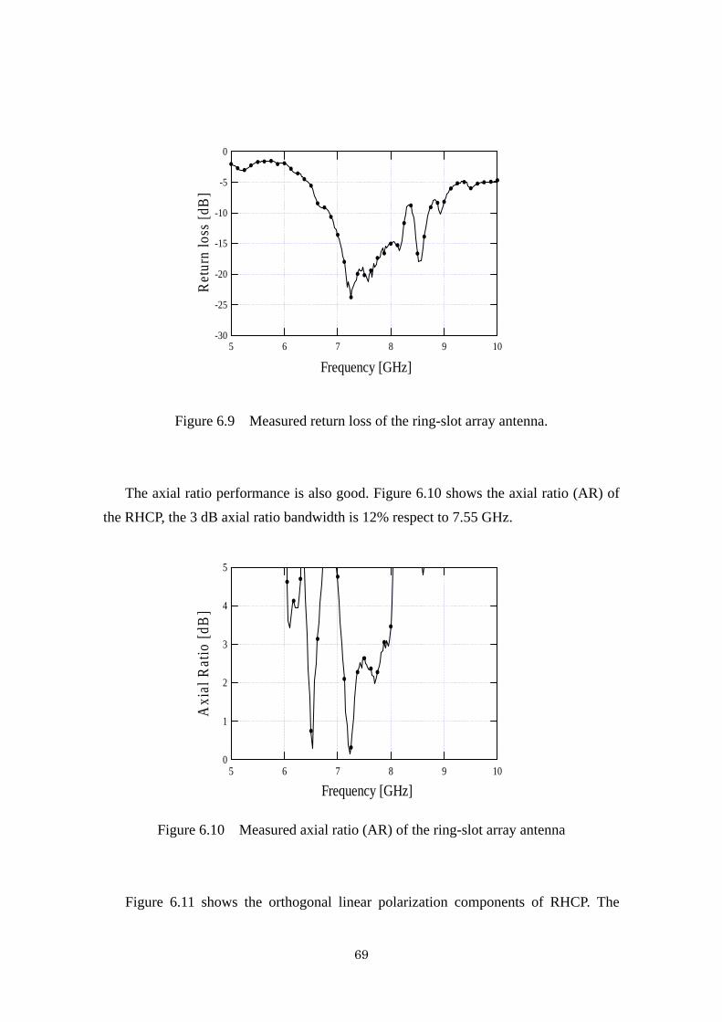
69
-30
-25
-20
-15
-10
-5
0
Ret
urn
loss
[dB
]
1098765
Frequency [GHz]
5
4
3
2
1
0
Axi
al R
atio
[dB
]
1098765
Frequency [GHz]
Figure 6.9 Measured return loss of the ring-slot array antenna.
The axial ratio performance is also good. Figure 6.10 shows the axial ratio (AR) of
the RHCP, the 3 dB axial ratio bandwidth is 12% respect to 7.55 GHz.
Figure 6.10 Measured axial ratio (AR) of the ring-slot array antenna
Figure 6.11 shows the orthogonal linear polarization components of RHCP. The

70
-40
-30
-20
-10
0
Rel
ativ
e Po
wer
[dB
]
-180 -120 -60 0 60 120 180
Angle θ [deg.]
xz yz
horizontal plane of the horn antenna is xz-plane, and the vertical plane of the horn
antenna is yz-plane. Both the horizontal (xz plane) and the vertical (yz plane) linear
polarization components are presented, and the two components are almost same.
Therefore the circular polarization is confirmed experimentally. Need less to say, the
LHCP can also be achieved by change the diodes state.
Figure 6.11 Radiation pattern of the ring-slot array antenna, RHCP
Frequency: 7.2 GHz
The experiment results for the proposed circular polarization switchable ring-slot
array antenna show a good polarization performance and broad bandwidth in this
chapter. The broadband performance is obtained mainly due to the use of the ring-slot
antenna elements and the Both-Side MIC technology. The good polarization
performance is realized by the symmetrical antenna structure.
6.4 Conclusion
In this chapter, a broad-band circular polarization switchable ring-slot array antenna
is described. A ring-slot array, a 90 degrees branch line hybrid circuit and a SPDT
switch circuit are integrated in the proposed antenna. Due to the controlling the diodes

71
state, the two kinds of circular polarization, that is, RHCP and LHCP can be switched
successfully. The excellent circular polarization performance can be obtained in a wide
frequency bandwidth. In addition, the antenna structure is very symmetrical, and the
antenna design is very simple.
Therefore, this type of array antenna is useful for wireless communication systems,
which involve circular polarization. Moreover, extending this array antenna structure,
sixteen elements array or thirty-two elements ring-slot array antenna with circular
polarization switching function can be easily realized as well.

72
Chapter 7
Conclusion
In this thesis, four kinds of array antennas with polarization agility and broadband
performance are proposed. The both-sided MIC technology is effectively employed in
forming these polarization agile planar antennas. These planar array antennas need no
impedance matching circuit in principle and have a very simple antenna design.
A novel 3 conductive layers 2×2 ring-slot array antenna is designed and utilized to
realize the simultaneous use of the orthogonal linear polarizations. Due to the use of the
characteristics of the ring-slot array antenna and features of the both-sided MIC
technology, excellent performances such as broad-band, good isolation, and better cross
polarization suppression are obtained. For the symmetrical antenna structure, two
orthogonal linear polarizations can be realized with same radiation pattern and same
polarization performance. In addition, the antenna design is very simple, and the array
antenna is easy to fabricate.
Using the characteristics of the ring-slot array antenna mentioned above, a novel
circular polarization ring-slot array antenna with simultaneous use of the orthogonal
polarizations is proposed. By integrating a broad-band 90 degrees hybrid circuit, the
array antenna can radiate two kinds of circular polarizations; that is, Left Hand Circular
Polarization (LHCP) and Right Hand Circular Polarization (RHCP) with good
polarization performance. Moreover, the circular polarization can be obtained in a very
wide frequency range. The 3 dB axial ratio bandwidths are wider than 25% (RHCP) and
29% (LHCP) and the impedance bandwidth is 47%.
And then a novel linear polarization switchable 2×2 ring-slot array antenna structure
has been successfully developed. Basing on the study of three conductive layers
ring-slot array antenna, a SPDT switch circuit is integrated in the array antenna to
compose an advanced array antenna, linear polarization switchable array antenna. By
using the SPDT switch circuit, the antenna can provide the switching function between

73
the φ = +45 degree and φ = -45 degree linear polarization. In this array antenna, ±45
degree linear polarizations can be realized with excellent cross polarization suppression
better than -20 dB.
In addition, a 90 degrees branch line hybrid circuit and a SPDT switch circuit are
integrated in the ring-slot array antenna to form a novel circular polarization switchable
ring-slot array antenna. The two kinds of circular polarizations (RHCP and LHCP) can
be switched with simple method. And the orthogonal circular polarization switchable
ring-slot array antenna is theoretically and experimentally verified.
The four kinds of polarization agile slot array antennas are realized for the first time
as far as the author knows. These results are very promising and suited for wireless
communication systems, RF sensors and radars, which need the orthogonal polarization
agility.

74
References
[1] X. Bao and M. J. Ammann, “Dual-frequency dual-sense circularly-polarized slot
antenna fed by microstrip line,” IEEE Trans. on Antennas and Propagation, vol. 56,
no. 3, pp. 645-649, March 2008.
[2] K. Sakamoto, E. Nishiyama, M. Aikawa, “Active microstrip planar antenna for
frequency switching,” IEICE Trans. Commun.(Japanese Edition), vol. J87-B, no. 11,
pp. 1918-1925, Nov. 2004.
[3] H. A. Ghali, and T. A. Moselhy, “Broad-band and circularly polarized
space-filling-based slot antennas,” IEEE Trans. Microw. Theory Tech., vol. 53, no. 6,
pp. 1946-1950, Jun. 2005.
[4] M. Aikawa, “Microstrip line directional coupler with tight coupling and high
directivity,” IEICE Trans., vol. 60-B, 4, pp. 253-259, 1977.
[5] M. Aikawa and H. Ogawa, “A New MIC-T using coupled slot lines,” IEEE Trans.
Microwave Theory Tech., vol MTT-28.pp.523-528, June 1980.
[6] Ito, K., N. Aizawa, and N. Goto, “Circularly polarized printed array antennas
composed of strips and slots,” Electron. Lett., vol. 15, pp. 811-812, 1979.
[7] Oliner, A. A., “The radiation conductance of a series slot in strip transmission line,”
IRE National Conv. Rec., vol. 2, part 8, pp. 89-90, 1954.
[8] Sommers, D. J., “Slot array employing photo-etched triplate transmission line,” IRE
Trans., vol. MTT-3, pp. 157-162, Mar. 1955.
[9] Proctor, D., “Some aspects of TEM slot design in strip line,” Proc. Array Antenna
Conf., Naval Electronics Laboratory Center, San Diego, CA, paper 35, Feb 1972.
[10] Rao, J. S., B. N. Das, “Impedance of off-centered strip line fed series slot,” IEEE

75
Trans. Antennas and Propagation, vol. AP-26, pp. 893-895, 1978.
[11] Chen, C., N. G. Alexopoulos, “Modeling microstrip line fed slot antennas with
arbitrary shape,” Electromagnetic, vol. 15, pp. 567-586, 1995.
[12] Axelrod, A., M. Kisliuk, J. Maos, “Broadband microstrip-fed slot radiator,”
Microwave J., pp. 81-94, June 1989.
[13] Bhattacharyya, A. K., Y. M. M. Antar, A. Ittipiboon, “Full wave analysis for the
equivalent circuit of an inclined slot on a microstrip ground plane,” Proc. IEE, vol.
139, pp. 245-250, Pt. H, 1992.
[14] Yoshimura, Y., “ A microstrip line slot antrnna,” IEEE Trans. Microwave Theory and
Techniques, vol. MTT-20, pp. 760-762, 1972.
[15] Pozar, D. M., “Reciprocity method of analysis for printed slot and slot-coupled
microstrip antennas,” IEEE Trans. Antennas and Propagation, vol. AP-34, pp.
1439-1446, 1986.
[16] Das, B. N., K. K. Joshi, “Impedance of a radiating slot in the ground plan of a
microstrip line,” IEEE Trans. Antennas and Propagation, vol. AP-30, pp. 922-926,
1982.
[17] Morishita, H., K. Hirasawa, K. Fujimoto, “Analysis of a cavity-backed annular slot
antenna with one point shorted,” IEEE Trans. Antennas and Propagation, vol.
AP-39, pp. 1472-1478, 1991.
[18] James, J. R., R. S. Hall (Eds.), Handbook of microstrip antennas, chapter 19, peter
peregrines, London, UK, 1989,
[19] Weiss, M. A., “Mirostrip antenna for millimeter wave,” IEEE Trans. Antennas and
Propagation, vol. AP-29, pp. 171-174, 1981.
[20] Bhartia, P., K. V. S. Rao, R. S. Tomar, Millimeter-wave microstrip and printed
circuit antennas, Artech House, Norwood, MA, 1991.

76
[21] Pozar, D.M, Microwave Engineering, John Wiley&Sons, New York, 1998.
[22] Warren L. Stutzman and Gary A. Thiele, Antenna Theory And Design.
[23] Kin-Lu, Wong, Compact and Broadband Microstrip Antennas, 2002.
[24] Constantine A. Balanis, Antenna theory-Analysis and design, Second Edition, 2005.
[25] M. Aikawa and H. Ogawa, “C Band MIC double-balanced modulator for 2Gbit/s
PSK,” in Proc. 1979 ISCAS, pp.818-821, July 1979.
[26] Y. Liu, Z. Shen, C. L. Law, “A compact dual-and cavity-backed slot antenna,” IEEE
Antennas Wireless Progap. Lett., vol. 5, pp.4-6, 2006.
[27] S. Y. Chen, P. Hsu, “Broad-band radial slot antenna fed by coplanar waveguide for
dual-frequency operation,” IEEE Trans. Antennas and Propagation, vol. 53, no. 11,
pp. 3448-3452, Nov. 2005.
[28] A. E. Fathy, “A novel planar polarized feed network for dual circular polarization,”
in Proc. IEEE AP-S Int. Symp. And USNC/URSI National Padio Science Meeting, vol.
1, pp. 412-415, 2001.
[29] F. Ferrero, C. Luxey, G. Jacquemod, R. Staraj, “Dual-band circularly polarized
microstrip antenna for satellite applications,” IEEE Antrenns Wireless Propag. Lett.,
vol. 4, pp. 13-15, 2005.
[30] M. Egashira, E. Nishiyama, M. Aikawa, “Microstrip array antenna using both-sided
MIC feed circuits,” 2002 Asia-pacific Microwave Conf. Proc., vol. 2, pp.
1288-1291, 2002.
[31] K. Kodama, E. Nishiyama, M. Aikawa, “Slot array antenna using both-sided MIC
technology,” Proc. 2004 IEEE AP-S int. Symp., vol. 3, pp. 2715-2718, 2004.
[32] F. Yang and Y. Rahmat-Samii, “A reconfigurable patch antenna using switchable
slots for circular polarization diversity,” IEEE Microwave Guided Wave Lett.,

77
vol.12. no.3, pp.96-98, March 2002.
[33] M. K. Fries, R. Vahldieck, “Uniplaner circularly polarized slot-ring antenna
architectures,” Radio Sci. vol.38, no.2, November 2002.
[34] M. Boit, L. Dusspot, and J. –M. Laheurte, ‘Circularly polarized antenna with
switchable polarization sence,’ Electron. Lett., vol. 36, no. 18, pp.1518-1519,
August 2005.
[35] X.M. Qing, Y.W.M.Chia, “Circularly polarized circular ring slot antenna fed by
stripline hybrid coupler,” Elect. Lett., vol. 35, no. 25, pp. 2154-2155, Dec. 9th,1999.
[36] J.S.Rpw, C.Y.D.Sim, K.W.Lin,: ‘Broadband printed ring-slot array with circular
polarization,’ Elect. Lett., vol. 41, no. 3, pp. 110-112, Feb. 3rd, 2005.
[37] F. C. de Ronde, “ A New Class of Microstrip Directional Couplers,” Digest of Tech.
Papers, G-MTT Symp., pp. 184-189, May 1970.
[38] M. Aikawa, H. Ogawa, “Double-Sided MIC’s and Their Applications,” IEEE Trans.
Microwave Theory and Tech., vol.37, no.2, pp.406-413, Feb. 1989.
[39] Jung D., Fukusako T., Kitamura N., Mita N., Ha C., “Polarization Switchable
Microstrip Antenna Using PIN Diodes,” IEICE Trans. Commun., vol. E87-B, no.1,
pp. 152-157, 2004.
[40] Haskins P. M., Dahele J. S., “Polarization, phase and frequency agility in varactor
diode loaded patch,” 2000 Asia-Pacific Microwave Conf. Proc., pp. 747-750, 2002.
[41] Schaubert D. H., Farrar F. G., Sindoris A., Hayes S. T., “Microstrip antenna with
Frequency agility and polarization diversity,” IEEE Trans. Antenna Propa., vol. 29,
no. 1, pp. 118-123, 1981
[42] Fries M. K., Grani M., Vahidieck R.,“A reconfiguration slot antenna with
switchable polarization,” Micro Wireless Compon. Lett., vol. 13, pp. 490-492,

78
2003.
[43] E. Nishiyama, M. Aikawa, S. Sasaki, “Polarizations switchable slot-ring array
antenna,” IET Microwave, Antenna & Propagation, vol. 2, no. 3, pp. 236-241, 2008