Embed Size (px)
Citation preview
ce
i@u
pm
.es
Universidad Politécnica de Madrid
Optimum Design of anEnvelope Tracking Buck
Converter for RF PA UsingGaN HEMTs
Dejana Čučak

2
Tercer Seminario Anual CEI
Mayo 2010
Introduction
Wireless and broadband services – growing on a daily basis!
Radio base stations – low efficiency!
Reason: poor efficiency of linear amplifier
Techiques in order to increase the efficiency:
Envelope TrackingEnvelope Elimination and
Restoration
IV Annual Meeting
2011 March

3
Tercer Seminario Anual CEI
Mayo 2010
Envelope Elimination and Restoration Technique
Envelope Amplifier in EER should have: Fast dynamic response
High efficiency
ENVELOPE AMPLIFIER
IV Annual Meeting
2011 March

4
Tercer Seminario Anual CEI
Mayo 2010
Synchronous Buck as an Envelope Amplifier
Wide Bandwidth → High Switching Frequency → High Losses! Very good Figure Of Merit of GaN HEMTs → Lower Losses!
GaN HEMTs
GaN: FOM=Qg*Ron=37.1 Si: FOM=Qg*Ron=174.6
IV Annual Meeting
2011 March

5
Tercer Seminario Anual CEI
Mayo 2010
Converter Design Requirements
PA
0 2 10 6−× 4 10 6−× 6 10 6−× 8 10 6−× 1 10 5−×0
0.2
0.4
0.6
0.8
1
Requirements: high corner frequency of the filter → high voltage and current ripple
1. Wide bandwidth high switching frequency → high losses → low efficiency
2. High efficiency
TRADE – OFF BETWEEN THE EFFICIENCY AND THE BANDWIDTH!
Chalenge: to design the filter in order to achieve this trade-off!
IV Annual Meeting
2011 March
6
Tercer Seminario Anual CEI
Mayo 2010
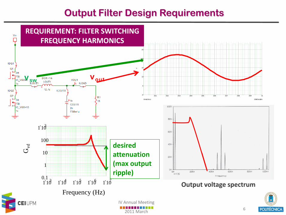
Output Filter Design Requirements
time/uSecs 100nSecs/div
20.1 20.2 20.3 20.4 20.5 20.6 20.7 20.8 20.9 21
V
-0
5
10
15
20
25
voutvsw
1 103´ 1 104´ 1 105´ 1 106´ 1 107´0.1
1
10
100
1 103´
Frequency (Hz)
Gvd desired
attenuation(max output ripple)
REQUIREMENT: FILTER SWITCHING FREQUENCY HARMONICS
IV Annual Meeting
2011 March
Output voltage spectrum
7
Tercer Seminario Anual CEI
Mayo 2010
Output Filter Design Requirements
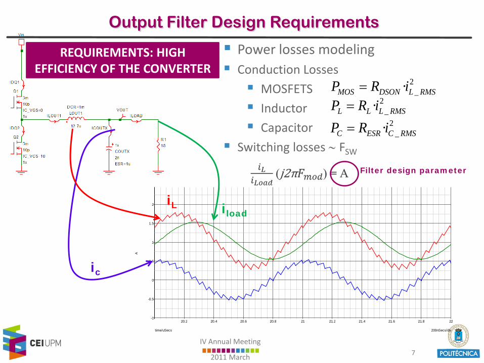
Power losses modeling Conduction Losses
MOSFETS
Inductor
Capacitor
Switching losses ∼ FSW
2_·MOS DSON L RMSP R i=
2_·L L L RMSP R i=
2_·C ESR C RMSP R i=
time/uSecs 200nSecs/div
20.2 20.4 20.6 20.8 21 21.2 21.4 21.6 21.8 22
A
-1
-0.5
0
0.5
1
1.5
2 iload
ic
iL
REQUIREMENTS: HIGH EFFICIENCY OF THE CONVERTER
IV Annual Meeting
2011 March
Filter design parameter

8
Tercer Seminario Anual CEI
Mayo 2010
Output Filter Design Requirements
How to minimize the losses byfilter design?
1 · ·LLoad out
Load
i R C si
= +
1 103× 1 104× 1 105× 1 106× 1 107× 1 108×0
1
2
3
Frequency (Hz)
IL/Io
1
Minimize conductionlosses→ minimize A!
Lout =? Cout =?
Lower A→lower Cout→higherbandwidth →higher switching
frequency!
IV Annual Meeting
2011 March
A
9
Tercer Seminario Anual CEI
Mayo 2010
Output Filter Design Requirements
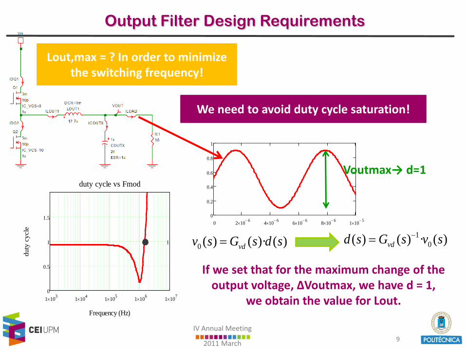
Lout,max = ? In order to minimizethe switching frequency!
0 ( ) ( )· ( )vdv s G s d s=
We need to avoid duty cycle saturation!
10( ) ( ) · ( )vdd s G s v s−=
0 2 10 6−× 4 10 6−× 6 10 6−× 8 10 6−× 1 10 5−×0
0.2
0.4
0.6
0.8
1
1 103× 1 104× 1 105× 1 106× 1 107×0
0.5
1
1.5
duty cycle vs Fmod
Frequency (Hz)
duty
cyc
le
1
If we set that for the maximum change of theoutput voltage, ∆Voutmax, we have d = 1,
we obtain the value for Lout.
IV Annual Meeting
2011 March
Voutmax→ d=1

10
Tercer Seminario Anual CEI
Mayo 2010
Output Filter Design: Experimental Results
Converter specifications:• Input voltage, Vin = 24V• Output voltage, Vout
Deviation, ∆Vout = 18VFrequency, Fmod = 200kHz
• Peak output power,Poutmax=25W• Ripple attenuation 27dB
Two filter designs:• A = 1.1• A = 1.4
The goal is to develop the lossesdependence on the filter design and to find
the minimum overall losses!
Switching losses are dominant!
IV Annual Meeting
2011 March
A=1.1 A=1.4
Fsw [MHz] 4.7 3.1
L [uH] 13 13.5
C [nF] 28 60
Plosses [W] 5.7 3.5

11
Tercer Seminario Anual CEI
Mayo 2010
Application of GaN HEMTs: Experimental Results
• Two EPC1015 GaN HEMTs• XILINX SPARTAN3 FPGA for generation of the control signals• The goal is operating frequency around 20MHz, in order to obtain the
bandwidth around 7MHz!
IV Annual Meeting
2011 March
GaN HEMTs

12
Tercer Seminario Anual CEI
Mayo 2010
Comparison of GaN and Si: Experimental Results
• The second prototype was made usingtwo Si MOSFETs from Infinieon withpreviously calculated FOM
• Both prototypes were made exactly thesame, regarding the PCB layout , isolation chips and drivers
• The only difference – transistors!
82%
0,5
0,55
0,6
0,65
0,7
0,75
0,8
0,85
0 5 10 15 20 25
effic
ienc
y
Pout[W]
4.7MHz
GaN
Si
61%61%
79.5%
GaN
Si
Lower overshoot → lowerleakage inductance of the
package
Vin=10V
Vin=10V
IV Annual Meeting
2011 March
12V
20V70%
50ns

13
Tercer Seminario Anual CEI
Mayo 2010
Comparison of GaN and Si: Experimental Results
• The GaN prototype was able to provideoutput voltage which corresponds to thechange of the duty cycle from 5% - 95%,at 5MHz of Fsw!
• Si prototype provided the sequence onlybetween 35% - 65%
• Reason – low current capability of thedriver. Gate pulses are distorted!GaN – lower Vth!
Vin=24V
Driver output
FPGA output
GaN prototype
IV Annual Meeting
2011 March
4V
23V
400ns

14
Tercer Seminario Anual CEI
Mayo 2010
Cooperation with ISOM
•ISOM is in charge of making the series of Enhancement mode GaN HEMTs
IV Annual Meeting
2011 March
•Future step: application of these GaN HEMTs!
15
Tercer Seminario Anual CEI
Mayo 2010
Summary
The goal of the research is the development of highly efficientEnvelope Amplifier for WCDMA and OFDM applications
In order to obtain the optimum trade-off between theefficiency and the achieved bandwidth, filter designmethodology is proposed
Comparing to Si MOSFETs, application of GaN HEMTsexperimentally showed higher efficiency at 5MHz
Future work1. Detail model of power losses for multivariable optimization of the
system2. Implementation of drivers with higher current capability in order to
increase the switching frequency
Thank you for your attention!IV Annual Meeting
2011 March

16
Tercer Seminario Anual CEI
Mayo 2010
Application of GaN HEMTs: Experimental Results
IV Annual Meeting
2011 March
x10
0
5
10
15
20
25
30
35
40
45
50
Pow
er L
oss
[mW
]
Power Loss at 1MHz, Pout=1.25W
Gate losses HS
Gate losses LS
Conduction losses HS
Conduction losses LS
Total switching losses
x100
0
5
10
15
20
25
30
35
Pow
er L
oss
[mW
]
Power Loss at 1MHz, Pout=12W
Gate losses High Side
Gate losses Low Side
Conduction losses High Side
Conduction losses Low Side
Total switching losses