Embed Size (px)
Citation preview

Optimizing the Design of Partially and Fully Depleted MESFETs for Low
Dropout Regulators
by
William Lepkowski
A Dissertation Presented in Partial Fulfillment
of the Requirements for the Degree
Doctor of Philosophy
ARIZONA STATE UNIVERSITY
December 2010
Optimizing the Design of Partially and Fully Depleted MESFETs for Low
Dropout Regulators
by
William Lepkowski
has been approved
September 2010
Graduate Supervisory Committee:
Trevor Thornton, Chair
Bertan Bakkaloglu
Michael Goryll
Raja Ayyanar
ACCEPTED BY THE GRADUATE COLLEGE

iii
ABSTRACT
The constant scaling of supply voltages in state-of-the-art CMOS
processes has led to severe limitations for many analog circuit applications. Some
CMOS processes have addressed this issue by adding high voltage MOSFETs to
their process. Although it can be a completely viable solution, it usually requires a
changing of the process flow or adding additional steps, which in turn, leads to an
increase in fabrication costs. Si-MESFETs (silicon-metal-semiconductor-field-
effect-transistors) from Arizona State University (ASU) on the other hand, have
an inherent high voltage capability and can be added to any silicon-on-insulator
(SOI) or silicon-on-sapphire (SOS) CMOS process free of cost. This has been
proved at five different commercial foundries on technologies ranging from 0.5 to
0.15 μm.
Another critical issue facing CMOS processes on insulated substrates is
the scaling of the thin silicon channel. Consequently, the future direction of
SOI/SOS CMOS transistors may trend away from partially depleted (PD)
transistors and towards fully depleted (FD) devices. FD-CMOS are already being
implemented in multiple applications due to their very low power capability.
Since the FD-CMOS market only figures to grow, it is appropriate that MESFETs
also be developed for these processes.
The beginning of this thesis will focus on the device aspects of both PD
and FD-MESFETs including their layout structure, DC and RF characteristics,
and breakdown voltage. The second half will then shift the focus towards

iv
implementing both types of MESFETs in an analog circuit application. Aside
from their high breakdown ability, MESFETs also feature depletion mode
operation, easy to adjust but well controlled threshold voltages, and fT’s up to 45
GHz. Those unique characteristics can allow certain designs that were previously
difficult to implement or prohibitively expensive using conventional technologies
to now be achieved. One such application which benefits is low dropout
regulators (LDO). By utilizing an n-channel MESFET as the pass transistor, a
LDO featuring very low dropout voltage, fast transient response, and stable
operation can be achieved without an external capacitance. With the focus of this
thesis being MESFET based LDOs, the device discussion will be mostly tailored
towards optimally designing MESFETs for this particular application.

v
TABLES OF CONTENTS
Page
LIST OF TABLES ............................................................................................... viii
LIST OF FIGURES ............................................................................................... ix
CHAPTER
1. INTRODUCTION ...........................................................................1
1.1. MESFET Device Structure ............................................1
1.2. MESFET Fabrication .....................................................4
1.3. Device Operation ...........................................................7
1.4. Threshold Voltage ........................................................12
1.5. Tradeoff Between Breakdown Voltage and
Transconductance Gain ................................................18
1.6. Conclusion ...................................................................21
2. SCALING PD-SOI MESFETs ......................................................22
2.1. Optimizing FD-MESFET Layout ................................22
2.2. DC Characterization.....................................................27
2.3. RF Characterization .....................................................32
2.4. MESFET Breakdown ...................................................37
2.5. Conclusion ...................................................................41
3. FD-SOI & SOS MESFETS ............................................................44
3.1. FD-MESFET Architecture ...........................................44
3.2. Regions of Device Operation .......................................49

vi
CHAPTER Page
3.3. Turn-On Characteristics ...............................................54
3.4. Breakdown Mechanisms ..............................................56
3.5. Layout Alternatives and Potential Improvements ........59
3.6. Modeling ......................................................................64
3.7. Conclusion ...................................................................69
4. N-MESFET LDO ...........................................................................70
4.1. PMOS LDO Overview .................................................71
4.2. NMOS LDO Overview ................................................76
4.3. N-MESFET LDO Overview ........................................80
4.4. Selecting N-MESFET Pass Device ..............................82
4.5. N-MESFET LDO Issues ..............................................83
4.6. Measurement Setup & PCB Board Design ..................87
4.7. Buffer Design and Transient Results ...........................91
4.8. PSRR Results ...............................................................93
4.9. Improving FD-MESFET LDOs ...................................94
4.10. Conclusions ..................................................................96
5. PD SOI MESFET LDOs ................................................................98
5.1. PD-MESFET LDO Overview ......................................99
5.2. MESFET Pass Transistor Characteristics ..................102
5.3. PD-MESFET LDO Results ........................................104
5.4. PD-MESFET LDO Results Across Temperature ......108

vii
CHAPTER Page
5.4. Low Voltage Opportunities and Body Bias
Effects ........................................................................111
5.5. Radiation Effects On MESFET LDO ........................114
5.6. Conclusion .................................................................118
6. CONCLUSION ............................................................................120
6.1. Optimizing MESFET Pass Transistor ........................120
6.2. Future LDO Opportunities .........................................122
6.3. Other Potential Applications For MESFETs .............123
6.4. Conclusion .................................................................124
REFERENCES ....................................................................................................126
APPENDIX
A ELECTRICAL CHARACTERISTICS OF SURFACE
MOUNT COMPONENTS USED ON PCB BOARDS
FOR TESTING PD AND FD-MESFET LDO .........................130
B BARE DIE PICTURE OF LARGE PASS DEVICE .....................136
C ADDITIONAL WIDE TEMPERATURE
MEASUREMENTS FROM HONEYWELL LDO ..................138
D ADDITIONAL RADIATION MEASUREMENTS FROM
HONEYWELL LDO ................................................................143
E 3-D LAYOUT OF THE PD-MESFET PASS TRANSISTOR ......147

viii
LIST OF TABLES
Table Page
1. Scaling of Key Layout Rules for SB-MESFETs .........................................26
2. Comparison of SB and BT-MESFETs in the 150 nm SOI CMOS
Process .......................................................................................................27
3. Area of MESFETs in Fig. 37a .....................................................................62
4. Area of MESFETs in Fig. 39a .....................................................................64
5. Improvements in Peregrine’s Newer Process ..............................................96
6. LDO Performance Summary .......................................................................97
7. Area of MESFETs in Fig. 62 .......................................................................99

ix
LIST OF FIGURES
Figure Page
1. Cross-sectional view of a PD-MESFET structure which uses silicide
block to create the SiO2 spacers. ............................................................2
2. Fabrication steps for n-type MOSFETs and MESFETs in typical
SOS or SOI CMOS processes [3]. .........................................................6
3. Cross-section of MESFET showing the lateral growth of the silicide
contacts and lateral diffusion of the source/drain implant [12]. ............7
4. FOC plot showing the different regions of operation for the
MESFET. The device is from a 350 nm SOI CMOS process
and has the following characteristics: W = 100 μm, Lg = 100
μm, and LaS = LaD = 0.6 μm. ..................................................................9
5. Shows the variation of the depletion region under different regions
of operation. a) VGS = 0 V and VDS = 0 V. b) Linear region. c)
Pinch-off. d) Saturation region. e) Subthreshold region. .....................10
6. From the drain current curves, it can be seen that the MESFET’s
threshold voltage is becoming more positive with increasing
gate length. Devices are from a 350 nm SOI CMOS process. .............14
7. The Gummel plot shows the changes in DC operation for a 100 μm
device with Lg = LaS = LaD = 0.6 μm between -60 to 150 ˚C.
The device is from a 350 nm SOI CMOS process. ..............................15
8. Structure of the MESFET PTAT used in [18]. ............................................17

x
9. The tradeoff of peak transconductance and breakdown voltage is
shown as a function of LaD. Devices are from a 350 nm SOI
CMOS process. ....................................................................................20
10. The transconductance of the device is greatly affected by LaS. The
degregation in transconductance can be minimized by
appropriately sizing LaS. Devices are from a 350 nm SOI
CMOS process. ....................................................................................20
11. Top-view of PD-MESFET layout with the gate contacted inside
the access region (silicide block is used to create the SiO2
spacers). ...............................................................................................23
12. Top-view of PD-MESFET layout with the gate contacted outside
the access region to reduce Lg (silicide block is used to create
the SiO2 spacers). .................................................................................23
13. Top-view of the BT PD-MESFET layout with the gate contacted
outside the access region to reduce Lg. ................................................26
14. Cross-sectional view of a PD-MESFET structure which uses the
body-tie method to create oxide spacers. .............................................27
15. Gummel plots for the smallest gate lengths fabricated on each
process: a) 350 nm SOI CMOS and b) 150 nm SOI CMOS. ..............28
16. Threshold voltage extracted for each of the devices plotted in Fig.
15a-b. ...................................................................................................30

xi
17a-d). Measured family of curve plots corresponding to the four
devices shown in Fig. 15b. In each graph the gate voltage is
stepped from +0.5 V (uppermost curve) to -0.5 V in 0.25 V
steps......................................................................................................31
18. Exhibits the trade-off in current drive and output resistance for the
MESFETs in Fig. 17a-d. ......................................................................32
19. The GSG structure used for RF characterization in the 150 nm
process..................................................................................................33
20. Shows the roll-off in transconductance gain as LaD increases from
300 nm to 1 µm on the 150 nm SOI CMOS process. ..........................34
21. Shows the exponential scaling of the peak cut-off frequencies for
MESFETs manufactured on 150 and 350 nm SOI CMOS
processes. .............................................................................................35
22. A comparison of the fT dependence on drain current for two
MESFETs with nominally identical dimensions but fabricated
using different SOI CMOS technology nodes. ....................................36
23. Shows the cut-off frequencies versus drain current for select
devices on the 150 nm SOI CMOS process. ........................................37
24. Shows the breakdown voltage of various MESFET structures on
the 150 nm SOI CMOS process. ..........................................................40

xii
25. The family of curves for a MESFET with Lg = 400 nm, LaS = 600
nm and LaD = 1 µm. The gate voltage is stepped from +0.4 V
(uppermost curve) to -0.4 V in 0.1 V steps. .........................................41
26. Comparison of Gummel plots for nominally identical Lg = 300 nm
devices fabricated on the 150 nm process in August 2008 and
May 2009. ............................................................................................43
27. 3-D rendering of the FD-SOI MESFET showing two conducting
channels confined between islands of silicide. Electrical
contact to each silicide island is provided by contacts to the
first layer of metal interconnect. ..........................................................46
28. Shows a cross-section in the y-z plane through the center of the
device. The conducting channels are formed underneath the
regions of silicide block. The current flows into the channels as
indicated in the figure. .........................................................................46
29. Threshold voltage of SOS MESFETs as a function of the channel
width. The dashed lines are linear fits to the data [27]. .......................49
30. Lateral depletion for various regions of device operation. a) VGS =
0 V and VDS = 0 V. b) Linear region. c) Pinch-off. d)
Saturation region. e) Subthreshold region. ..........................................52
31. Depletion growth from top view [13]. a) VGS = 0 V and VDS = 0 V.
b) Linear region. c) Pinch-off. d) Saturation region. e)
Subthreshold region. ............................................................................53

xiii
32. Family of curves plot showing regions of MESFET operation. ................54
33. The turn-on characteristics, ID-VGS for a) n-MESFETS (VDS = 2 V)
and b) p-MESFETs (VDS = -2 V) for different channel widths.
The insets show the magnitude of the gate current for LCW =
0.25 µm. ...............................................................................................55
34. The family of curves plot for a) the n-MESFET and b) the p-
MESFET for gate voltages in the range of -0.5 to +0.5 V in 0.1
V steps. LgN = 1.8 µm, LCW
N = 0.25 µm, Lg
P = 1.8 µm, and
LCWP = 0.25 µm. ...................................................................................57
35. Compares the FOC for two devices that are nominally the same but
with different doping profiles. The heavier doping improved
the current drive and output resistance, but reduced the
breakdown of the device. .....................................................................59
36. 3-D rendering a FD-MESFET which extends silicide block into the
gate region to reduce the effective gate length. ...................................61
37. a) Compares two devices, that are nominally similar expect one
utilizes the structure in Fig. 27 and the other uses Fig. 36. b)
Compares the two devices after they have been normalized to
current per unit area. ............................................................................61
38. 3-D rendering of a FD-MESFET showing silicide block being
offset in order to reduce the effective gate length................................63

xiv
39. a) Compares the Gummel plots of three devices with different gate
offsets on the MIT-LL process. b) Compares the same devices
after they have been normalized to current per unit area. ....................63
40. Screen shot of how to change gmin in Cadence’s Analog Design
Environment. ........................................................................................65
41. Large signal model of a MESFET with the TOM3 sub-circuit. IBGD
and IBDS are used to model the breakdown voltage in the circuit
[23]. ......................................................................................................66
42. Compares the measured results (solid line) to the simulated model
(open circles) for the family of curves plot. .........................................67
43. Compares the Gummel plots of the measured results (solid line) to
the simulated model (open circles). .....................................................67
44. Compares the measured results (solid line) to the simulated model
(open circles) for the drain current vs. gate voltage at VD = 2 V. ........68
45. Compares the gm of the measured results (solid line) to the
simulated model (open circles) at VD = 2 V. .......................................68
46. Basic circuit schematic of a LDO using a P-channel pass transistor
in a common source configuration. The LDO has been
compensated through CLoad and RESR [26]. ..........................................72
47. Range of stability chart for the Texas Instruments TPS76301 LDO.
CSR refers to the ESR from the capacitor plus any external
resistor if applicable [34]. ....................................................................74
xv
48. Includes the key internal parasitic components as well as the added
external components that affect the stability of the PMOS LDO
system. .................................................................................................75
49. Closed-loop gain response of a compensated LDO utilizing a
PMOS pass transistor. ..........................................................................76
50. Circuit schematic of an LDO using a NMOS pass transistor in a
common drain configuration. ...............................................................78
51. Includes the key internal parasitic components that affect the
stability of the NMOS LDO system.....................................................78
52. Closed-loop gain response of an LDO utilizing a NMOS pass
transistor. ..............................................................................................79
53. Schematic of the LDO regulator using an N-MESFET pass
transistor. ..............................................................................................81
54. Measured and simulated drain and gate current of the scaled down
MESFET used in the LDO. ..................................................................83
55. Measured total dropout voltage resulting from the PMOS power-
down switch and N-MESFET pass device. Also shown is the
contribution from only the PMOS switch. ...........................................84
56. Measured ground current and current efficiency versus load
current. At higher loads the current efficiency approaches 99%. ........86
57. Multisim schematic of the PCB test board. ...............................................89
xvi
58. a) Die micrograph of the LDO. b) Picture of the bonded LDO on a
gold-plated PCB. ..................................................................................90
59. Measured line regulation for both the low-to-high, a), and high-to-
low transitions, b). The output voltage settles in less than ≤ 800
ns. .........................................................................................................92
60. Measured load regulation for both the low-to-high, a), and high-to-
low transitions, b). The output voltage settles in less than ≤ 1
µs. .........................................................................................................93
61. PSRR for loads of 10.8 and 34 mA............................................................94
62. a) Compares MESFETs from FD and PD technologies to exhibit
the gain in current drive and reduction in gate current with PD-
MESFETs. b) Compares the two in Part a) after they have been
normalized............................................................................................99
63. Simple circuit schematic of the board level LDO design with a
picture of the bonded out die. The device excluding pads is
0.73 x 0.55 mm while the cavity of the DIP-8 package is 7.37 x
4.32 mm. ............................................................................................100
64. PCB test board for the PD-MESFET LDO. .............................................101
65. Schematic of PCB board used to test the PD-MESFET LDO. ................102
66. Gummel plot of bonded out PD-MESFET pass transistor.......................103
67. a) FOC for MESFET pass transistor. b) FOC of MESFET that is
1/28 the size of the pass transistor. ....................................................104

xvii
68. a) Ground current with the low Iq error amplifier. b) Ground
current with the low Iq error amplifier at light loads. ........................105
69. Transient line regulation with the low Iq error amplifier. Iout = 50
mA, tr = tf = 200 ns and T = 50 µs. ....................................................106
70. Transient line regulation with the moderate Iq error amplifier. Iout =
50 mA, tr = tf = 200 ns and T = 50 µs. ...............................................107
71. Transient load regulation with the low Iq error amplifier. Vin = 2.4
V, tr = tf = 500 ns and T = 50 µs. .......................................................107
72. Transient load regulation with the moderate Iq error amplifier. Vin
= 2.4 V, tr = tf = 500 ns and T = 50 µs. ..............................................108
73. Line regulation at -50, 25, and +150oC at a load of 50 mA. ....................109
74. Load regulation at -50, 25, and +150oC at a Vin = 2.4 V. ........................110
75. The dropout voltage was measured up to 100 mA for -50, 25, and
+150oC and extrapolated from 100 to 150 mA. .................................110
76. a) Ground current at 85oC with the low Iq error amplifier. b)
Ground current at 85oC with the low Iq error amplifier at light
loads. ..................................................................................................111
77. Compares the MESFET pass transistor at two different bulk-to-
source voltages. ..................................................................................113
78. Compares the dropout voltage when the substrate of the MESFET
is biased at 0 V and 1.8 V. .................................................................113

xviii
79. Compares the Gummel plot of MESFET pass device after an
exposure dose of 1 Mrad(Si). .............................................................115
80. a) DC line regulation at various cumulative radiation exposures. b)
Zoom in of Part a). .............................................................................116
81. a) DC load regulation at various cumulative radiation exposures. b)
Zoom in of Part a). .............................................................................117
82. The output voltage of the PD-MESFET LDO at cumulative
radiation doses of 10, 20, 50, 100, 200, 500, and 1000 krad(Si). ......117
83. Electrical characteristics of the 2N3904 BJT. The 2N3094 was
used with the Honeywell and Peregrine LDO to switch in a
load for the load transient response. Refer to [45] for the
complete datasheet. ............................................................................131
84. The electrical characteristics of the NCS2001 operational amplifier
which was used as the moderate Iq error amplifier in the
Honeywell LDO. Refer to [46] for the complete datasheet. ..............132
85. The electrical characteristics of the LMP2231 operational amplifier
which was used as the low Iq error amplifier in the Honeywell
LDO. Refer to [47] for the complete datasheet. .................................135
86. Picture of bare die which includes the large MESFET device
(upper left corner). Excluding pads, the MESFET is 0.73 x 0.55
mm. ....................................................................................................137

xix
87. The regulated output voltage of the Honeywell MESFET regulator
was defined at a nominal load of 50 mA and measured over the
temperature range of -50 to +150C. .................................................139
88. The line regulation in V/V from -50 to +150oC. ......................................139
89. The load regulation in mV/mA from -50 to +150oC. ..............................140
90. Transient load regulation with the moderate Iq error amplifier at -
50oC. Vin = 2.4 V, tr = tf = 500 ns and T = 50 µs. ..............................140
91. Transient load regulation with the moderate Iq error amplifier at
+150oC. Vin = 2.4 V, tr = tf = 500 ns and T = 50 µs. ..........................141
92. Transient line regulation with the moderate Iq error amplifier at -
50oC. Iout = 50 mA, tr = tf = 200 ns and T = 50 µs. ............................141
93. Transient line regulation with the moderate Iq error amplifier at
+150oC. Iout = 50 mA, tr = tf = 200 ns and T = 50 µs. ........................142
94. Dropout voltage verses total ionizing dose at a load of 50 mA. ..............144
95. Transient line regulation with the moderate Iq error amplifier after
1 Mrad(Si). Iout = 50 mA, tr = tf = 200 ns and T = 50 µs. ..................145
96. Transient load regulation with the moderate Iq error amplifier after
1 Mrad(Si). Vin = 2.4 V, tr = tf = 500 ns and T = 50 µs. ....................145
97. Load regulation comparing the MESFET LDO immediately after 1
Mrad(Si) and after 24 hours of annealing. .........................................146
98. Line regulation comparing the MESFET LDO immediately after 1
Mrad(Si) and after 24 hours of annealing. .........................................146

xx
99. Layout of two interdigitated fingers. .......................................................149
100. Shows a zoom in of Fig. 99. ..................................................................149
101. Shows 4 of the 28 rows in the PD-MESFET pass transistor. ................150
102. Zooms in on one section of Fig. 101 to show the source, drain,
and gate lines......................................................................................150
103. Removes the entire drain line and some of the metal layers of the
source and gate lines in Fig. 102 to show how individual
fingers connect to the bus lines. .........................................................151
104. Shows a zoomed in picture of Fig. 103 as well the via stack which
connects the drain lines of the MESFET fingers (M1) to the
drain bus line (M2-M6). .....................................................................152

1
CHAPTER 1
INTRODUCTION
Si-MESFETs from ASU show significant promise for a variety of analog
circuit applications due to their ability to be easily fabricated and integrated with
SOS and SOI CMOS without changing any of the steps in a process flow [1-3].
Different reports [4-6] have considered Si-MESFETs on SOI, SOS, and bulk
CMOS processes but in each case none of them were able to use a standard
CMOS process flow. When comparing them to GaAs MESFETs, the enhanced
performance must be considered with the high cost it takes to fabricate them
along with their inability to integrate well with other devices. While the ASU
MESFETs cannot compete with GaAs MESFET at microwave frequencies they
do appear to be a strong low cost contender for analog applications below 10
GHz. This chapter gives a brief introduction to PD-MESFETs with a discussion
on their structure, fabrication, operation, and basic DC characteristics.
1.1. MESFET DEVICE STRUCTURE
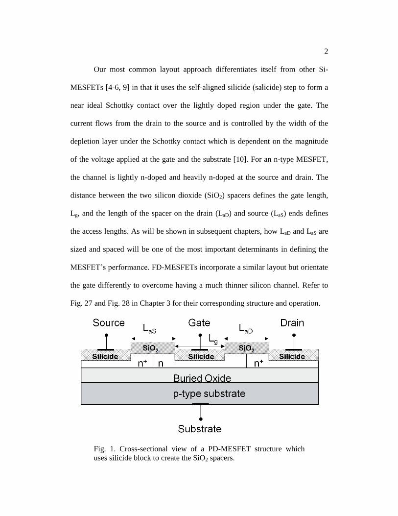
PD-MESFETs, like the one shown in Fig. 1, are four terminal majority
carrier devices. This is in contrast to GaAs MESFETs which are three terminal
devices due to their much thicker insulating layer which shields the effects of
biases applied to the substrate [7]. Also, by being a PD device, the thickness of
the active silicon layer is greater than the depletion width under the gate [8].
2
Our most common layout approach differentiates itself from other Si-
MESFETs [4-6, 9] in that it uses the self-aligned silicide (salicide) step to form a
near ideal Schottky contact over the lightly doped region under the gate. The
current flows from the drain to the source and is controlled by the width of the
depletion layer under the Schottky contact which is dependent on the magnitude
of the voltage applied at the gate and the substrate [10]. For an n-type MESFET,
the channel is lightly n-doped and heavily n-doped at the source and drain. The
distance between the two silicon dioxide (SiO2) spacers defines the gate length,
Lg, and the length of the spacer on the drain (LaD) and source (LaS) ends defines
the access lengths. As will be shown in subsequent chapters, how LaD and LaS are
sized and spaced will be one of the most important determinants in defining the
MESFET’s performance. FD-MESFETs incorporate a similar layout but orientate
the gate differently to overcome having a much thinner silicon channel. Refer to
Fig. 27 and Fig. 28 in Chapter 3 for their corresponding structure and operation.
Fig. 1. Cross-sectional view of a PD-MESFET structure which
uses silicide block to create the SiO2 spacers.
3
Perhaps the most important parameter with respect to the MESFET’s
ability to operate is the thickness of the silicon channel. If the channel is too thin
then the current drive is very low. On the other hand, if it is too thick, then the
MESFET has little gate control and cannot pinch itself off. Based on a series of
fabrication runs with various manufacturers, the ideal channel thickness for PD-
MESFETs appears to be about 100 – 200 nm [2-3, 11]. That thickness in turn,
usually corresponds to threshold voltages, Vt, somewhere in the manageable
range of -0.5 to -1.5 V. Due to that channel thickness range, bulk CMOS
technologies cannot be used for this type of MESFET fabrication. It is also why
incorporating a technology with a thin silicon film on top of an insulting layer
such as SOI or SOS is absolutely necessary. Refer to Section 1.3 for more on the
device operation.
Among other advantages of using an SOI or SOS technology over
traditional bulk silicon is it provides higher frequency operation and lower power
consumption. This is the result of the insulating layer reducing the overall
parasitic capacitance and blocking the leakage path to the substrate. At higher
temperatures, CMOS designed on bulk silicon can be limited by the large leakage
current in the well junction which in turn can lead to latch-up [10]. Since
MESFETs and CMOS alike are inherently insulated on SOI or SOS, they can be
packed closer together in layout which helps offset some of the increased
fabrication costs incurred by incorporating an insulating layer [8].
4
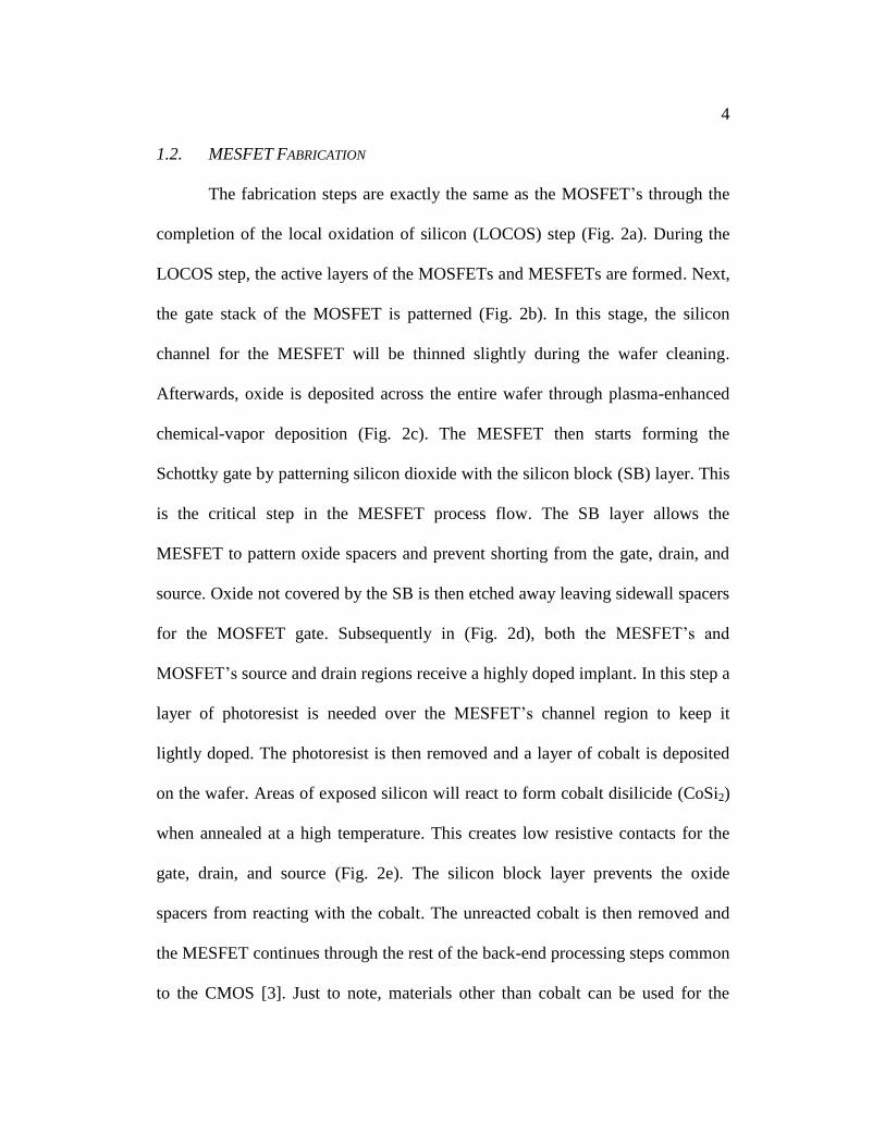
1.2. MESFET FABRICATION
The fabrication steps are exactly the same as the MOSFET’s through the
completion of the local oxidation of silicon (LOCOS) step (Fig. 2a). During the
LOCOS step, the active layers of the MOSFETs and MESFETs are formed. Next,
the gate stack of the MOSFET is patterned (Fig. 2b). In this stage, the silicon
channel for the MESFET will be thinned slightly during the wafer cleaning.
Afterwards, oxide is deposited across the entire wafer through plasma-enhanced
chemical-vapor deposition (Fig. 2c). The MESFET then starts forming the
Schottky gate by patterning silicon dioxide with the silicon block (SB) layer. This
is the critical step in the MESFET process flow. The SB layer allows the
MESFET to pattern oxide spacers and prevent shorting from the gate, drain, and
source. Oxide not covered by the SB is then etched away leaving sidewall spacers
for the MOSFET gate. Subsequently in (Fig. 2d), both the MESFET’s and
MOSFET’s source and drain regions receive a highly doped implant. In this step a
layer of photoresist is needed over the MESFET’s channel region to keep it
lightly doped. The photoresist is then removed and a layer of cobalt is deposited
on the wafer. Areas of exposed silicon will react to form cobalt disilicide (CoSi2)
when annealed at a high temperature. This creates low resistive contacts for the
gate, drain, and source (Fig. 2e). The silicon block layer prevents the oxide
spacers from reacting with the cobalt. The unreacted cobalt is then removed and
the MESFET continues through the rest of the back-end processing steps common
to the CMOS [3]. Just to note, materials other than cobalt can be used for the

5
silicide step; however, it will affect the MESFET’s work function and therefore
its operation. Refer to [12] for an excellent discussion on different silicides with
ASU’s MESFETs.

6
Fig. 2. Fabrication steps for n-type MOSFETs and MESFETs in
typical SOS or SOI CMOS processes [3].
7
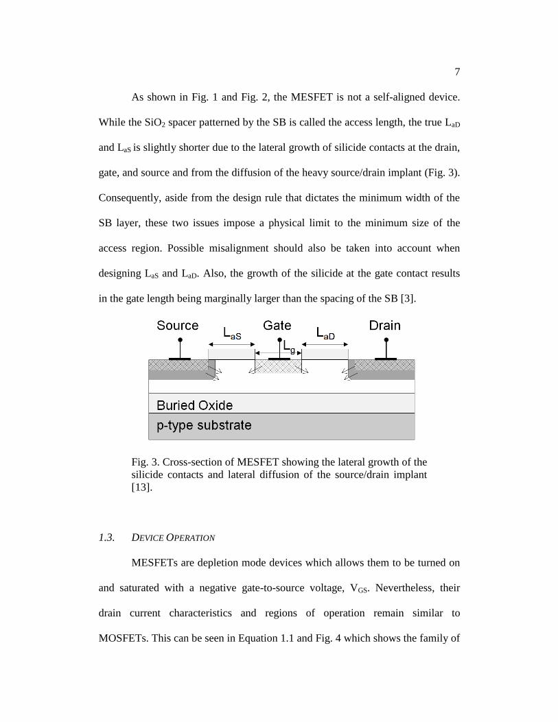
As shown in Fig. 1 and Fig. 2, the MESFET is not a self-aligned device.
While the SiO2 spacer patterned by the SB is called the access length, the true LaD
and LaS is slightly shorter due to the lateral growth of silicide contacts at the drain,
gate, and source and from the diffusion of the heavy source/drain implant (Fig. 3).
Consequently, aside from the design rule that dictates the minimum width of the
SB layer, these two issues impose a physical limit to the minimum size of the
access region. Possible misalignment should also be taken into account when
designing LaS and LaD. Also, the growth of the silicide at the gate contact results
in the gate length being marginally larger than the spacing of the SB [3].
Fig. 3. Cross-section of MESFET showing the lateral growth of the
silicide contacts and lateral diffusion of the source/drain implant
[13].
1.3. DEVICE OPERATION
MESFETs are depletion mode devices which allows them to be turned on
and saturated with a negative gate-to-source voltage, VGS. Nevertheless, their
drain current characteristics and regions of operation remain similar to
MOSFETs. This can be seen in Equation 1.1 and Fig. 4 which shows the family of

8
curves (FOC) of one particular MESFET. Like a MOSFET, the MESFET follows
a square law dependence above threshold and is affected by channel length
modulation in the saturation region. The hyperbolic tangent function dominates in
the linear region (Equation 1.2) when the drain-to-source voltages, VDS, are small,
but it quickly approaches unity. Thus, it can be neglected in the saturation region
(Equation 1.3).
)tanh()1()( 2
DSDStGSD VVVVI (1.1)
)tanh()( 2
DStGSD VVVI (1.2)
)1()( 2
DStGSD VVVI (1.3)
where
β = transconductance gain
λ = channel length modulation
α = saturation factor
9
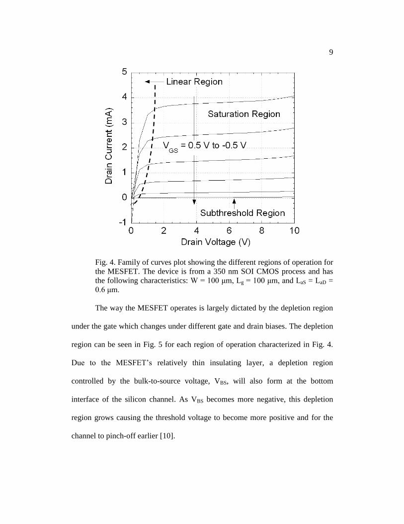
Fig. 4. Family of curves plot showing the different regions of operation for
the MESFET. The device is from a 350 nm SOI CMOS process and has
the following characteristics: W = 100 μm, Lg = 100 μm, and LaS = LaD =
0.6 μm.
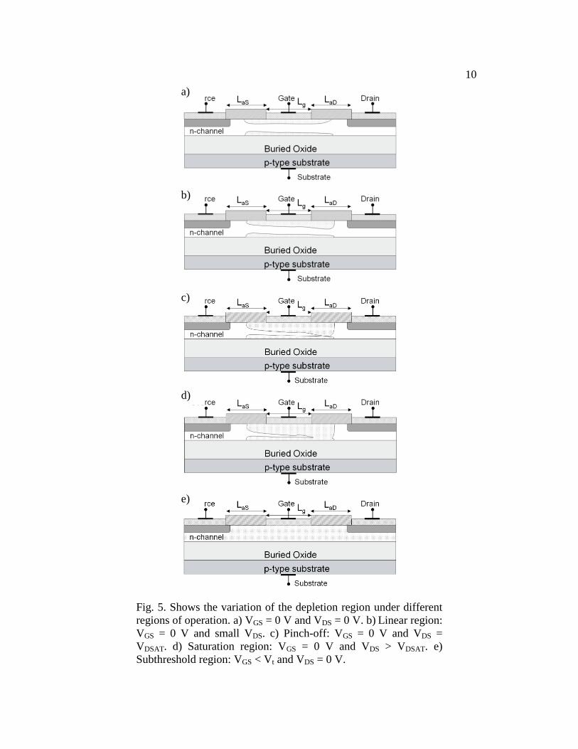
The way the MESFET operates is largely dictated by the depletion region
under the gate which changes under different gate and drain biases. The depletion
region can be seen in Fig. 5 for each region of operation characterized in Fig. 4.
Due to the MESFET’s relatively thin insulating layer, a depletion region
controlled by the bulk-to-source voltage, VBS, will also form at the bottom
interface of the silicon channel. As VBS becomes more negative, this depletion
region grows causing the threshold voltage to become more positive and for the
channel to pinch-off earlier [10].
10
Fig. 5. Shows the variation of the depletion region under different
regions of operation. a) VGS = 0 V and VDS = 0 V. b) Linear region:
VGS = 0 V and small VDS. c) Pinch-off: VGS = 0 V and VDS =
VDSAT. d) Saturation region: VGS = 0 V and VDS > VDSAT. e)
Subthreshold region: VGS < Vt and VDS = 0 V.
c)
b)
d)
e)
a)
11
In the linear region which is characterized by low drain voltages and gate
voltages above threshold, the drain current, ID, increases proportionally with drain
voltage at a fixed gate bias causing the MESFET to act like a resistor. As the
drain voltage increases, the junction between the drain and the gate becomes more
reversed biased causing the depletion region to widen faster towards the drain
side. Consequently, the channel narrows at drain end and leads to the slope of the
drain current rounding off (Fig. 4). The end of the linear region is marked by the
touching of the top and bottom depletion regions. At that point the channel
becomes pinched-off. Increasing the drain voltage any further saturates the
current. Similarly to MOSFETs, the drain current in this region will increase
slightly with drain voltage due to the effective channel length being reduced. As
VGS becomes more negative the depletion width increases due to the drain-gate
junction becoming more reversed biased. This in turn causes the channel region to
reduce, leads to smaller slopes of ID in the linear region, and causes the MESFET
to pinch-off at lower drain voltages [10, 14].
The last region of concern is the sub-threshold region. In this region the
channel is fully depleted, but small amounts of current can still flow as a result of
carriers in the space charge region [10]. As shown in Equation 1.4, the drain
current varies exponentially with gate voltage. This region has been exploited by
weakly inverted CMOS for ultra-low power applications, but due to the
considerable reduction in drain current and transconductance gain, the operational
frequency is usually limited to only a few MHz. On the other hand, the

12
MESFET’s lightly doped channel leads to a larger mobility and cutoff frequencies
5-6 times larger than the weakly inverted CMOS with the same gate length and
drain current [15]. Thus the MESFETs also show potential as micropower devices
[16]. From the standpoint of the LDO, the MESFET pass transistor is a high
power transistor and only enters the subthreshold region when the load is
discounted or under very light load conditions. A subthreshold operated MESFET
based error amplifier could be designed though for an ultra-low current LDO
where power consumption considerably trumps transient line and load recovery
speed.
)1)(tanh()( 22
DSDS
nU
VVV
D VVeI T
DStGS
(1.4)
where
γ = threshold-shifting parameter
n = ideality factor
UT = thermal voltage (UT = kT/q)
1.4. THRESHOLD VOLTAGE
Another interesting aspect of MESFETs is their well controlled but easy to
adjust threshold voltage and the number of ways it can be accomplished. The first
way involves biasing the substrate to purposely take advantage of the body effect
PD-MESFETs are prone to seeing as a result of their relatively thin buried oxide
layer. This option is not available in GaAs MESFETs since their insulting layer is
13
sufficiently thick [10]. The next option includes changing the thickness of the
MESFET’s silicon channel. The thicker the channel is, the more negative the
gate-source bias needs to be to pinch the channel off. This of course might not be
a desired route for PD-MESFETs since it involves the changing of process steps.
Not only will that alter the operation of the CMOS devices on the die, but it could
also add a physical cost to the fabrication. In the case of FD-MESFETs, the
devices are laterally depleting so their channel thickness can easily be altered with
no changes in the process. The last option comes about from the sizing of the gate
length. As the gate length approaches the minimum feature size of the process, the
MESFETs start to become heavily affected by short channel effects (SCE) (refer
to Fig. 16). In Fig. 6, the effect of the gate length on four otherwise similar
devices can be seen in the turn on of the drain current.

14
10-6
10-5
10-4
10-3
10-2
-1.5 -1.0 -0.5 0.0 0.5 1.0
Lg = 0.4 m
Lg = 0.6 m
Lg = 1.2 m
Lg=5 m
VD = 2 V
LaS
= LaD
= 1 m
W = 100 m
Dra
in C
urr
en
t (A
)
Gate Voltage (V)
Fig. 6. From the drain current curves, it can be seen that the
MESFET’s threshold voltage is becoming more positive with
increasing gate length. Devices are from a 350 nm SOI CMOS
process.
The MESFET’s ability to be able to easily generate large threshold voltage
differences makes them potentially attractive for proportional to absolute
temperature (PTAT) voltage references. PTATs can be difficult to design in
standard CMOS processes since BJT and JFET transistors are generally not
available and the threshold voltage difference in CMOS transistors is usually
small. Alternatively, parasitic pn junctions can be used, but their electrical
characteristics may not be controlled closely during fabrication [17].
In practice, PTATs are often matched with complementary to absolute
temperature (CTAT) references in BGRs to cancel out the voltage drift in each
reference to get a composite reference with very little drift [17-18]. With the
15
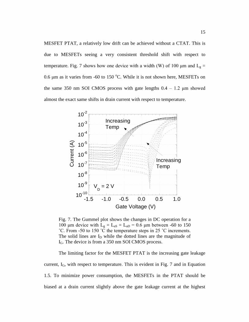
MESFET PTAT, a relatively low drift can be achieved without a CTAT. This is
due to MESFETs seeing a very consistent threshold shift with respect to
temperature. Fig. 7 shows how one device with a width (W) of 100 μm and Lg =
0.6 μm as it varies from -60 to 150 oC. While it is not shown here, MESFETs on
the same 350 nm SOI CMOS process with gate lengths 0.4 – 1.2 μm showed
almost the exact same shifts in drain current with respect to temperature.
10-10
10-9
10-8
10-7
10-6
10-5
10-4
10-3
10-2
-1.5 -1.0 -0.5 0.0 0.5 1.0
Curr
ent
(A)
Gate Voltage (V)
IncreasingTemp
IncreasingTemp
VD = 2 V
Fig. 7. The Gummel plot shows the changes in DC operation for a
100 μm device with Lg = LaS = LaD = 0.6 μm between -60 to 150
˚C. From -50 to 150 ˚C the temperature steps in 25 ˚C increments.
The solid lines are ID while the dotted lines are the magnitude of
IG. The device is from a 350 nm SOI CMOS process.
The limiting factor for the MESFET PTAT is the increasing gate leakage
current, IG, with respect to temperature. This is evident in Fig. 7 and in Equation
1.5. To minimize power consumption, the MESFETs in the PTAT should be
biased at a drain current slightly above the gate leakage current at the highest

16
rated temperature. From Equation 1.5 it can be seen that the gate leakage current
scales with the transistor’s size so it can be reduced with smaller transistors.
Unfortunately for the pass transistor of the LDO this means the gate leakage will
be several magnitudes larger and can become very appreciable at high
temperatures.
T
GS
T
B
nU
V
U
G eeTAAI
2* (1.5)
where
A = conducting area
A* = Richardson constant
T = temperature
ΦB = Schottky barrier
In [12], a relatively crude MESFET PTAT (Fig. 8) was built with the Lg =
0.6 and 1.2 µm devices from Fig. 6 to prove this concept. The two devices were
both discrete and were wire-bonded to a single 16-pin DIP (dual in-line pin)
socket. A circuit board was then designed with an off-the-shelf error amplifier to
complete the design. Even with this simplistic design, the MESFET PTAT had a
drift of only 11 ppm/oC from 25 to 100
oC when the bias current was set to 30 µA.
While that would be unacceptable for a lot of applications, particularly because of
the current consumption, the room for improvement is large. By integrating the
two MESFETs together along with the error amplifier, needless resistance from
the bond pads, wire bonds, and various wire connections which all have their own

17
temperature coefficient will go away. Furthermore, the two devices can be
optimally sized and ratio-ed to lower the leakage current and so they both can
operate at the same point on the drain curve to lower variation.
Vdd
+
_
Vref
I1 I2
Fig. 8. Structure of the MESFET PTAT used in [12].
For an LDO, a voltage reference is an absolutely necessary building block
and is needed for setting the output voltage. In the case of the fully integrated FD-
MESFET LDO presented in Chapter 4, an all CMOS BGR was used since it was
far less risky. Often manufacturers will alter process parameters from run-to-run
to enhance the CMOS operation, but they do not always release that information
for proprietary reasons. Without knowing these changes, variations in the
MESFET operation can occur which makes designing a high precision reference
difficult. Also the LDO’s targeted output voltage, 2 V, and maximum input
supply voltage, 3 V, were below the CMOS breakdown. Nevertheless, if a high
voltage LDO is desired, an all or mostly all MESFET LDO can be designed.

18
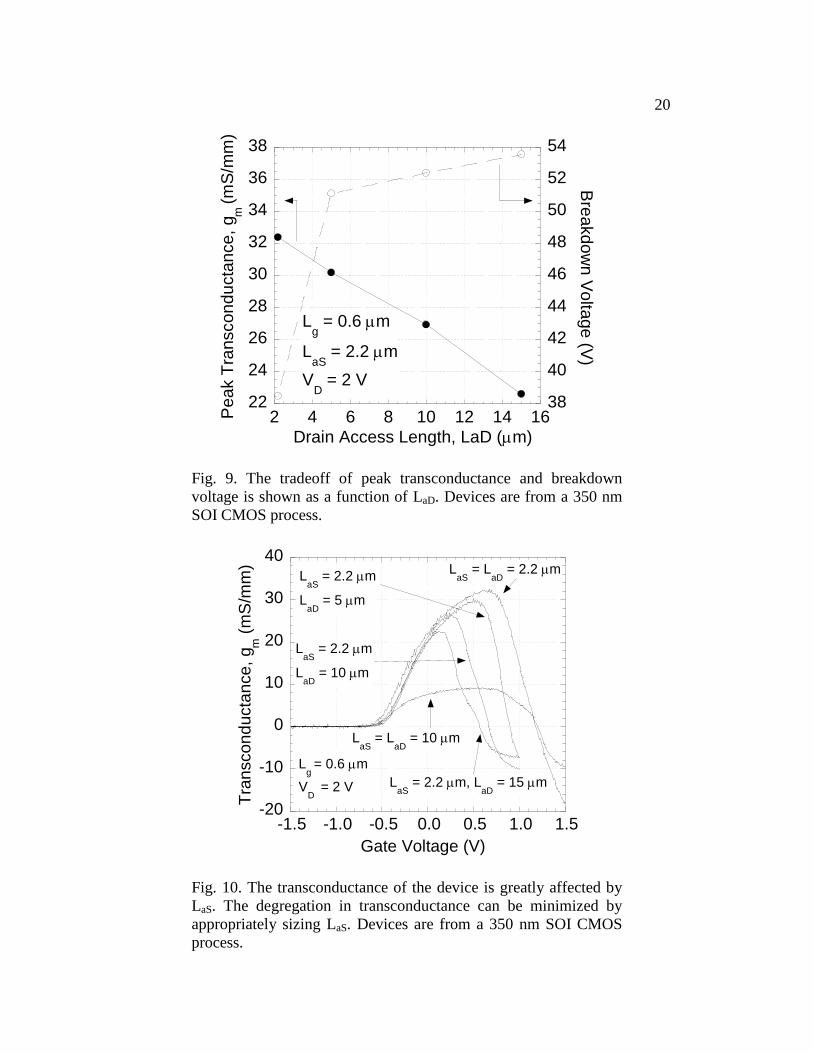
1.5. TRADEOFF BETWEEN BREAKDOWN VOLTAGE AND TRANSCONDUCTANCE GAIN
For most applications the biggest selling point of these MESFETs is they
offer a cost free way to increase the operating voltage of the process beyond the
capability of the CMOS transistors. From Fig. 9, it can be seen that MESFETs on
a 350 nm and 3.3 V SOI CMOS process were able to obtain breakdown voltages
in excess of 50 V. For the most part, this large breakdown voltage derives from
the sizing of the access regions. The function of the access regions is similar to
the drift region in a laterally depleted (LD) MOSFET which is to decrease the
electric fields between the drain-gate and source-gate junctions [1]. Since the
electric fields are disproportionate at the two junctions under most operating
conditions, the access regions do not need to be or should not be sized the same
unless LaS and LaD are sized at the minimum SB width. Increasing the access
regions beyond what is needed for a given operating voltage only serves to
degrade the performance of the device with respect to its transconductance gain,
gm, and peak cutoff frequency, fT. The reason being is the access regions act like
parasitic resistors in series with the channel and increase proportionately with
size.
The critical access length is LaD since the drain-gate junction becomes
more strongly reverse biased as the drain voltage increases resulting in a higher
electric field. As will be explained in detail in Section 2.4, there does appear to be
a critical size for which LaS needs to be to achieve high breakdowns, but after
which it contributes very little to the overall breakdown. Similarly there exists a

19
certain LaD where further gains in breakdown become negligible and the costs in
terms of layout size and degradation in performance become prohibitive. For the
350 nm SOI CMOS process this LaD is probably between 4 and 6 µm (Fig. 9). It is
hard to determine the exact length since the only lengths fabricated with LaD > 2
µm were 5, 10, and 15 µm.
The degradation from sizing LaS is quite evident in Fig. 10 for the two
devices with the LaD of 10 µm. The peak transconductance decreases from ~27
mS/mm to ~9.2 mS/mm as LaS increases from 2.2 to 10 µm even though both
devices will have approximately the same breakdown. In contrast, if LaS remains
at 2.2 µm and just LaD increases from 2.2 µm to 10 µm the peak transconductance
will reduce only from ~32.4 mS/mm to 27 mS/mm, but the breakdown voltage
increases from 38.5 to 52.4 V. The disproportionate effects of LaS and LaD can be
attributed to LaS also acting as a source degeneration resistor.
20
22
24
26
28
30
32
34
36
38
38
40
42
44
46
48
50
52
54
2 4 6 8 10 12 14 16
Bre
akd
ow
n V
olta
ge (V
)
Drain Access Length, LaD (m)
Pe
ak T
ran
sco
nd
ucta
nce
, g
m (m
S/m
m)
Lg = 0.6 m
LaS
= 2.2 m
VD = 2 V
Fig. 9. The tradeoff of peak transconductance and breakdown
voltage is shown as a function of LaD. Devices are from a 350 nm
SOI CMOS process.
-20
-10
0
10
20
30
40
-1.5 -1.0 -0.5 0.0 0.5 1.0 1.5
LaS
= LaD
= 2.2 mL
aS = 2.2 m
LaD
= 5 m
LaS
= 2.2 m
LaD
= 10 m
LaS
= 2.2 m, LaD
= 15 m
Lg = 0.6 m
VD
= 2 V
Gate Voltage (V)
Tra
nsco
nd
ucta
nce
, g
m (
mS
/mm
) LaS
= LaD
= 2.2 m
LaS
= LaD
= 10 m
Fig. 10. The transconductance of the device is greatly affected by
LaS. The degregation in transconductance can be minimized by
appropriately sizing LaS. Devices are from a 350 nm SOI CMOS
process.
21
1.6. CONCLUSION
As it was shown in this chapter, one of the main advantages of the
MESFET is its ease to tailor it to different applications by appropriately sizing
LaD, LaS, and Lg. The discussion and measured results were limited to only n-
MESFETs, however, p-MESFETs can be fabricated in an analogous way to Fig.
2. In general though, the p-MESFETs that have been fabricated have suffered
from higher gate leakage current and lower current drive, but having the
availability of p-MESFETs makes these SOI and SOS MESFETs unique to GaAs
MESFETs [19-20]. Hopefully with future research and subsequent fabrication
runs ideal complementary transistor operation can be obtained. Nevertheless, the
focus for this thesis will remain on optimizing n-MESFETs since p-MESFETs are
not encompassed in the LDOs presented in Chapters 4 and 5.
22
CHAPTER 2
SCALING PD-SOI MESFETs
PD-MESFET demonstrations have been made with SOI technologies at
the 600 nm [3] and 350 nm CMOS technology nodes [1]. This chapter presents
the latest measured data taken from MESFETs fabricated using a 150 nm PD-SOI
CMOS process from Honeywell. These devices represent the most aggressively
scaled and highest performing Si-MESFETs to date with gate lengths as short as
150 nm. Where it is applicable, the results are compared to those from devices
fabricated using the earlier 350 nm technology node which was also done at the
same foundry. Since MESFETs will undoubtedly scale at a different rate than the
MOSFETs due to the differences in device structure and layout layers used, this
comparison provides a statistical based insight into the MESFET’s performance
improvement from one technology node to the next and sets possible future
exceptions for Si-based MESFETs.
2.1. OPTIMIZING FD-MESFET LAYOUT
Like a CMOS transistor, the RF performance and current drive capability
of a MESFET is highly dependent on the minimum gate length that can be
achieved. In addition to the design rule that dictates the minimum spacing of the
patterned silicide block layers, other possible limiting factors on gate length are as
follows: the size of the contact layer which contacts the silicide layer at the gate to
Metal 1 (first level of metal in the process), the required Metal 1 overlap of the
contact, and the spacing between the contact layer and the spacer (Fig. 11).
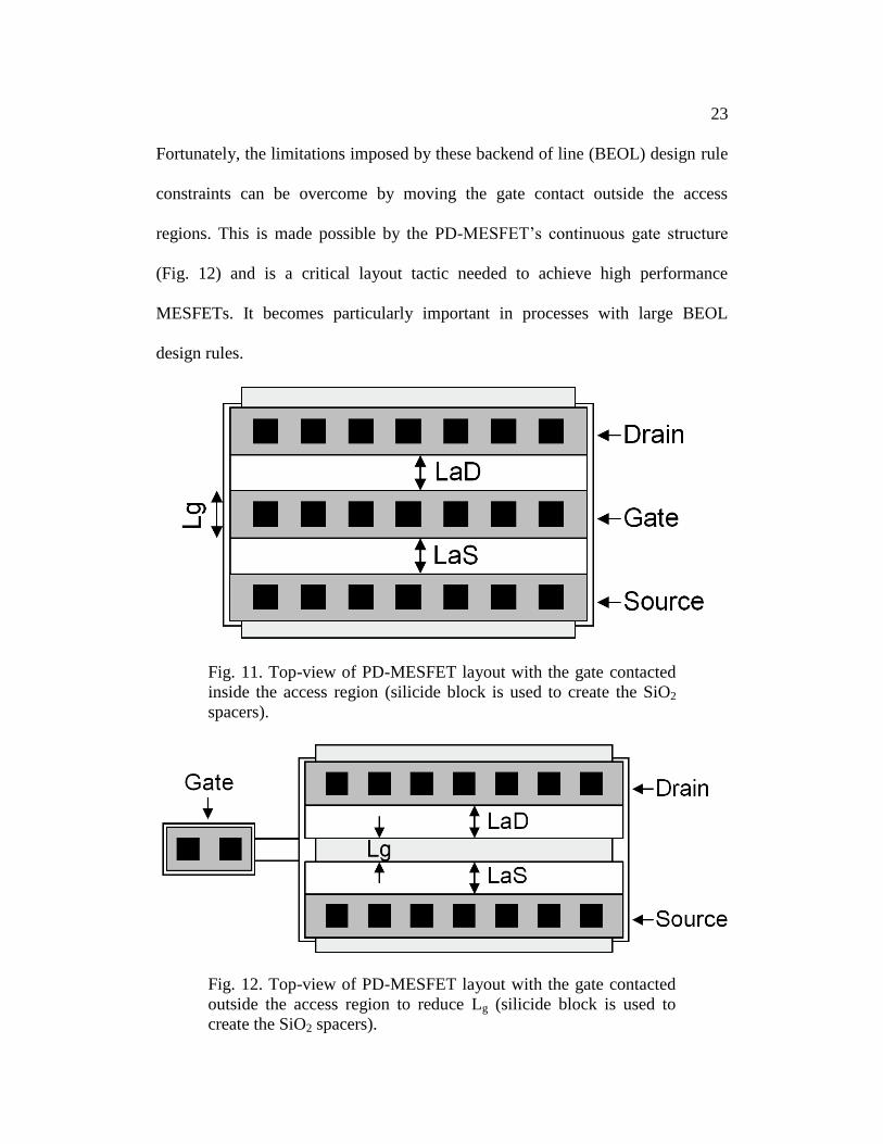
23
Fortunately, the limitations imposed by these backend of line (BEOL) design rule
constraints can be overcome by moving the gate contact outside the access
regions. This is made possible by the PD-MESFET’s continuous gate structure
(Fig. 12) and is a critical layout tactic needed to achieve high performance
MESFETs. It becomes particularly important in processes with large BEOL
design rules.
Fig. 11. Top-view of PD-MESFET layout with the gate contacted
inside the access region (silicide block is used to create the SiO2
spacers).
Fig. 12. Top-view of PD-MESFET layout with the gate contacted
outside the access region to reduce Lg (silicide block is used to
create the SiO2 spacers).

24
BEOL rules, nevertheless, will still have an effect on the length of the
drain and source lines which will consequently affect the MESFET in the form of
current drive per area. The drain current per finger will roughly be the same no
matter what the BEOLs are since it is mostly dictated by gate length (assuming
the structure in Fig. 12 is used), but the length of the drain and source lines will
affect how many fingers can fit into a given die area. This impact will be
relatively small for applications using small width MESFETs, for example < 1
mm, but for an application such as the pass transistor of an LDO which can easily
use MESFETs of several thousand fingers, the BEOLs rules can positively or
negatively affect the LDO’s commercial practicality. This subject will be further
discussed in much more detail in Chapters 4 and 5.
It is expected, however, that the device in Fig. 12 will have a higher noise
figure than the one in Fig. 11 due to it having a more resistive gate which is
caused by the elongated gate finger, fewer gate contacts, and the contacts being
placed at edge of the device. Thus in general, if the MESFET is going to be used
in a low-noise application, Fig. 11 would probably be a more advisable layout
option. In the 150 nm process, the drastic reduction in contact size and other
BEOL rules allows for Fig. 11 to be used without significantly increasing the gate
length. From Table 1, that was clearly not the case for the 350 nm process whose
minimum Lg would be 1.1 µm with the layout structure in Fig. 11. In that process,
even with the noise penalty of Fig. 12, the gains in current drive and RF
performance make Fig. 12 clearly more advantageous.

25
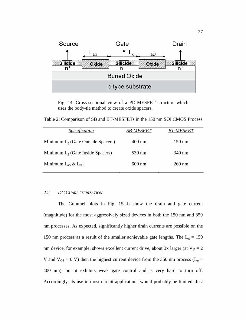
In the 150 nm process, the layout structure was slightly altered from the
typical PD-MESFET approach for the most aggressively scaled devices. Instead
of creating the access regions with silicide block which has a minimum width of
0.6 µm (refer to Fig. 11 and Fig. 12 structures), a body-tie (BT) approach
developed by Honeywell engineers was used. The BT-MESFET, shown in Fig.
13, surrounds the device with a body-tie. In regions where there is active silicon,
it is silicided. Elsewhere, the process etches the silicon above the buried oxide
down to about 45 nm and fills it with deposited oxide (Fig. 14). Therefore the BT
over non-active silicon areas, in effect, acts similarly to the function of the silicide
block; however, the rules that control the minimum separation and width of active
silicon are much more controlled in this process allowing for much smaller values
for LaS, LaD, and Lg. In fact, using this method allows for gate lengths as low as
150 nm and access lengths as small as 260 nm. The improvements between the
two structures are shown in Table 2. As was the case with SB-MESFETs, the gate
can be contacted both inside (not shown) and outside (Fig. 13) the oxide spacers
for BT-MESFETs. If the equivalent structure to Fig. 11 is used then the minimum
gate length becomes 340 nm.

26
Table 1: Scaling of Key Layout Rules for SB-MESFETs
Specification 350 nm SOI CMOS 150 nm SOI CMOS
Contact Size 300 x 300 nm 170 x 170 nm
M1 Overlap of Contact 225 nm 90 nm
Spacing of Contact and SB 400 nm 180 nm
Minimum Lg (Fig. 11) 1.1 µm 530 nm
Minimum Lg (Fig. 12) 400 nm 400 nm
Minimum LaS & LaD 600 nm 600 nm
Fig. 13. Top-view of the BT PD-MESFET layout with the gate
contacted outside the access region to reduce Lg.
27
Fig. 14. Cross-sectional view of a PD-MESFET structure which
uses the body-tie method to create oxide spacers.
Table 2: Comparison of SB and BT-MESFETs in the 150 nm SOI CMOS Process
Specification SB-MESFET BT-MESFET
Minimum Lg (Gate Outside Spacers) 400 nm 150 nm
Minimum Lg (Gate Inside Spacers) 530 nm 340 nm
Minimum LaS & LaD 600 nm 260 nm
2.2. DC CHARACTERIZATION
The Gummel plots in Fig. 15a-b show the drain and gate current
(magnitude) for the most aggressively sized devices in both the 150 nm and 350
nm processes. As expected, significantly higher drain currents are possible on the
150 nm process as a result of the smaller achievable gate lengths. The Lg = 150
nm device, for example, shows excellent current drive, about 3x larger (at VD = 2
V and VGS = 0 V) then the highest current device from the 350 nm process (Lg =
400 nm), but it exhibits weak gate control and is very hard to turn off.
Accordingly, its use in most circuit applications would probably be limited. Just

28
to note, each of the devices from Fig. 15 used the layout structure shown in Fig.
12 so that the performance of the devices with the same architecture could be
compared.
10-6
10-4
10-2
100
102
-2 -1.5 -1 -0.5 0 0.5 1Gate Voltage (V)
Curr
ent
(mA
/mm
)
Lg = 400 nm
LaS
= LaD
= 1 m
Lg = L
aS = L
aD = 600 nm
VD = 2 V
10-6
10-4
10-2
100
102
-2 -1.5 -1 -0.5 0 0.5 1
Lg = 150 nm
VD = 2 V
LaS
= LaD
= 300 nm
Lg = 300 nm
Lg = 400 nm
Lg = 200 nm
Curr
ent
(mA
/mm
)
Gate Voltage (V)
Fig. 15. Gummel plots for the smallest gate lengths fabricated on
each process: a) 350 nm SOI CMOS and b) 150 nm SOI CMOS.
Interestingly, when the two devices in Fig. 15 with gate lengths of 400 nm
are compared, the device on the 150 nm process has a noticebly smaller drain
current. This might be particularly suprising since the device on the 150 nm has
smaller access lengths which corresponds to a smaller parastic resistance in each
access region. That should correlate in theory to a higher drain current; however,
it does not account for threshold voltage difference in the two devices. The
threshold of the device on the 350 nm process is more negative which allows the
device to be turned on harder and have a higher drain current. Nevertheless, the
current drive per die area will be significantly higher on the newer process due to
the scaled BEOL rules and access legnths.
a) b)

29
From Fig. 15b its evident that the most aggressively sized gate lengths on
the 150 nm process were heavily affected by short channel effects. The gate
length at which SCE ceases to be an issue becomes clearer in Fig. 16 which
extracts the threshold voltage, Vt, for each of the MESFETs in Fig. 15a-b. From
the figure we conclude that gate lengths 400 nm are required to avoid SCE
altogether in the 150 nm technology, while Lg 600 nm is required for the 350
nm process. Presumably, the SOI channel in the 150 nm technology is thinner and
more heavily doped than in the older 350 nm technology allowing the 150 nm
node MESFETs to be scaled to shorter gate lengths before SCE become
significant. This observation is consistent with the threshold voltage model
developed by Chiang et al. for short-channel SOI MESFETs [21] which shows
the SCE becoming apparent as the gate length approaches the thickness of the
silicon channel [9]. Based on measured results from five different commercial
CMOS foundries [1-3], our MESFETs usually see SCE starting at 1.5 – 2x the
minimum feature size of the process. It will vary slightly on different processes
due to channel thickness, doping densities and the silicide step which consumes a
portion of the silicon channel. By interpolating the data in Fig. 16, a MESFET
with a gate length of 250 nm fabricated using the 150 nm node would have a
threshold voltage of approximately -1 V and represents a good trade-off between
high speed performance and practical depletion mode operation.
30
-2.5
-2.0
-1.5
-1.0
-0.5
0.0
0 0.2 0.4 0.6 0.8 1
Th
resh
old
Vo
ltag
e, V
t (V
)
Gate Length (m)
0.15 m SOI CMOS Process
0.35 m SOI CMOS Process
Fig. 16. Threshold voltage extracted for each of the devices plotted
in Fig. 15a-b.
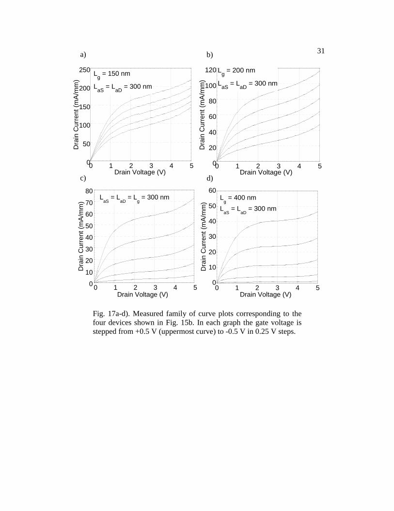
Pronounced SCE are also apparent in the family of curves plots in Fig.
17a-d. The slope of the drain current curves for the Lg = 150 nm MESFET in the
saturation region is indicative of a device with low output resistance. Also, the
requirement of a large drain voltage, ~2 V, before it reaches saturation suggests
that it has a large negative threshold which is consistent with the data in Fig. 16.
Fig. 18 plots the extracted output resistances of the devices considered in Fig. 17.
Again it appears that an ideal gate length is probably between 200 and 300 nm.
31
0
50
100
150
200
250
0 1 2 3 4 5
Dra
in C
urr
ent
(mA
/mm
)L
g = 150 nm
LaS
= LaD
= 300 nm
Drain Voltage (V)
0
20
40
60
80
100
120
0 1 2 3 4 5Drain Voltage (V)
Lg = 200 nm
LaS
= LaD
= 300 nm
Dra
in C
urr
ent (m
A/m
m)
0
10
20
30
40
50
60
70
80
0 1 2 3 4 5Drain Voltage (V)
LaS
= LaD
= Lg = 300 nm
Dra
in C
urr
ent (m
A/m
m)
0
10
20
30
40
50
60
0 1 2 3 4 5
Lg = 400 nm
LaS
= LaD
= 300 nmD
rain
Curr
ent
(mA
/mm
)
Drain Voltage (V)
Fig. 17a-d). Measured family of curve plots corresponding to the
four devices shown in Fig. 15b. In each graph the gate voltage is
stepped from +0.5 V (uppermost curve) to -0.5 V in 0.25 V steps.
a) b)
c) d)

32
0
4
8
12
16
0
5
10
15
20
0.1 0.2 0.3 0.4 0.5 0.6
Dra
in C
urr
en
t (m
A)
(VD =
2 V
& V
GS =
0 V
)
Outp
ut R
esis
tance (k
Ohm
s)
Gate Length, Lg (m)
Fig. 18. Exhibits the trade-off in current drive and output resistance
for the MESFETs in Fig. 17a-d.
2.3. RF CHARACTERIZATION
RF characterization was performed by on-wafer probing using select
devices with ground-signal-ground (GSG) pad configurations (Fig. 19). Also
included on the die was an accompanying set of open- and short-circuit test
structures to de-embed the devices and remove the parasitics of the GSG pads.
Measurements were taken by an Agilent 8510C vector network analyzer and a HP
8515a S-parameter test set. From the de-embedded S-parameters, WinCal [22]
was used to extract the fT of the MESFETs which was defined as the point where
the current gain, |h21|2, equaled 0dB. Since the Agilent 8510C only had a
measuring range of 0.45 – 20.3 GHz, devices with |h21|2 > 0 dB at 20.3 GHz had
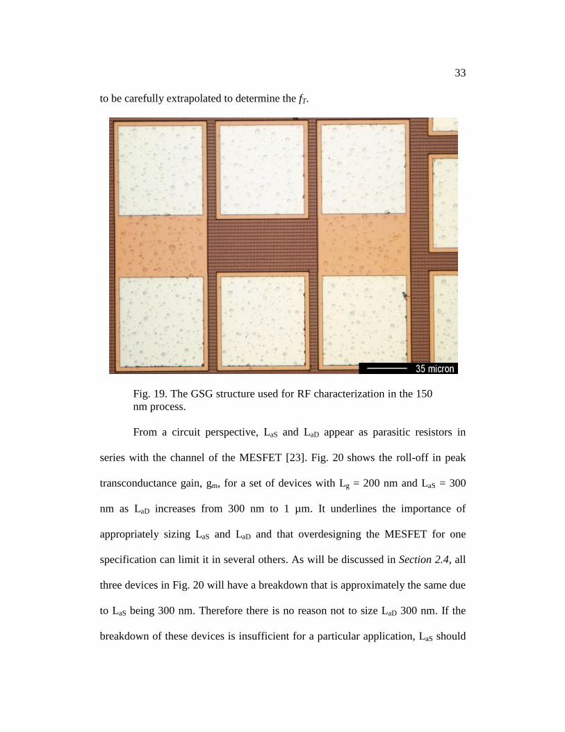
33
to be carefully extrapolated to determine the fT.
Fig. 19. The GSG structure used for RF characterization in the 150
nm process.
From a circuit perspective, LaS and LaD appear as parasitic resistors in
series with the channel of the MESFET [23]. Fig. 20 shows the roll-off in peak
transconductance gain, gm, for a set of devices with Lg = 200 nm and LaS = 300
nm as LaD increases from 300 nm to 1 µm. It underlines the importance of
appropriately sizing LaS and LaD and that overdesigning the MESFET for one
specification can limit it in several others. As will be discussed in Section 2.4, all
three devices in Fig. 20 will have a breakdown that is approximately the same due
to LaS being 300 nm. Therefore there is no reason not to size LaD 300 nm. If the
breakdown of these devices is insufficient for a particular application, LaS should

34
be sized to the critical length discussed in Section 2.4 and LaD should be sized
accordingly.
0
20
40
60
80
100
120
-1.5 -1 -0.5 0 0.5 1
Gate Voltage (V)
Tra
nsco
nd
ucta
nce
, g
m (
mS
/mm
)
Lg = 200 nm, L
aS = 300 nm
LaD
= 300 nm
LaD
= 800 nm
LaD
= 1 m
VD = 2 V
Fig. 20. Shows the roll-off in transconductance gain as LaD
increases from 300 nm to 1 µm on the 150 nm SOI CMOS process.
The cut-off frequencies of the devices in Fig. 15a-b are shown in Fig. 21.
This figure also includes a device with Lg = 1.2 µm and LaS = LaD = 1 µm
manufactured on the 350 nm process to show the trend in fT for the 350 nm
devices. It is encouraging that the exponential scaling with respect to gate length
holds in each process. This bodes well for the next technology node. The main
improvements can be traced to the reduction in the parasitic resistance of the
access regions due to the scaling of LaD and LaS and the reduction of parasitic
capacitance contributed by reduced size of the BEOL dimensions at the drain and
source. It is clear from Fig. 21 that there is a ~3x increase in the corresponding fT
values for the MESFETs with Lg = 400 and 600 nm manufactured using the 150
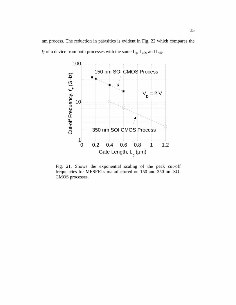
35
nm process. The reduction in parasitics is evident in Fig. 22 which compares the
fT of a device from both processes with the same Lg, LaD, and LaS.
1
10
100
0 0.2 0.4 0.6 0.8 1 1.2
Cut-
off F
requ
ency, f T
(G
Hz)
Gate Length, Lg (m)
150 nm SOI CMOS Process
350 nm SOI CMOS Process
VD = 2 V
Fig. 21. Shows the exponential scaling of the peak cut-off
frequencies for MESFETs manufactured on 150 and 350 nm SOI
CMOS processes.

36
0
5
10
15
20
10-4
10-3
10-2
Lg = L
aS = L
aD = 600 nm
150 nm SOI CMOS Process
350 nm SOI CMOS Process
VD = 2 V
Cut-
off
Fre
qu
en
cy, f T
(G
Hz)
Drain Current (A)
Fig. 22. A comparison of the fT dependence on drain current for
two MESFETs with nominally identical dimensions but fabricated
using different SOI CMOS technology nodes.
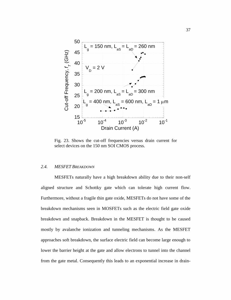
Fig. 23 displays the fT versus drain current for three devices that best
summarize the range of performance on the 150 nm process. The Lg = 150 nm and
LaS = LaD = 260 nm MESFET represents the highest measured fT device on the die.
The Lg = 200 nm and LaS = LaD = 300 nm MESFET has a lower fT, but as it was
shown in Fig. 15-Fig. 18, it balances the SCE shortcomings of the Lg = 150 nm
device and still maintains a relatively high current drive. An argument could be
made for the Lg = 300 nm device from Fig. 15b but it was not included with a
GSG structure and could not be characterized in the RF domain. Based on an
interpolation from Fig. 21, the fT is estimated to be ~35 GHz. Lastly, the Lg = 400
nm MESFET was included to show a device that nicely balances high breakdown
(~11 V) with peak fT.
37
15
20
25
30
35
40
45
50
10-5
10-4
10-3
10-2
10-1
Cu
t-o
ff F
req
ue
ncy, f T
(G
Hz)
Drain Current (A)
Lg = 150 nm, L
aS = L
aD = 260 nm
Lg = 200 nm, L
aS = L
aD = 300 nm
Lg = 400 nm, L
aS = 600 nm, L
aD = 1 m
VD = 2 V
Fig. 23. Shows the cut-off frequencies versus drain current for
select devices on the 150 nm SOI CMOS process.
2.4. MESFET BREAKDOWN
MESFETs naturally have a high breakdown ability due to their non-self
aligned structure and Schottky gate which can tolerate high current flow.
Furthermore, without a fragile thin gate oxide, MESFETs do not have some of the
breakdown mechanisms seen in MOSFETs such as the electric field gate oxide
breakdown and snapback. Breakdown in the MESFET is thought to be caused
mostly by avalanche ionization and tunneling mechanisms. As the MESFET
approaches soft breakdown, the surface electric field can become large enough to
lower the barrier height at the gate and allow electrons to tunnel into the channel
from the gate metal. Consequently this leads to an exponential increase in drain-
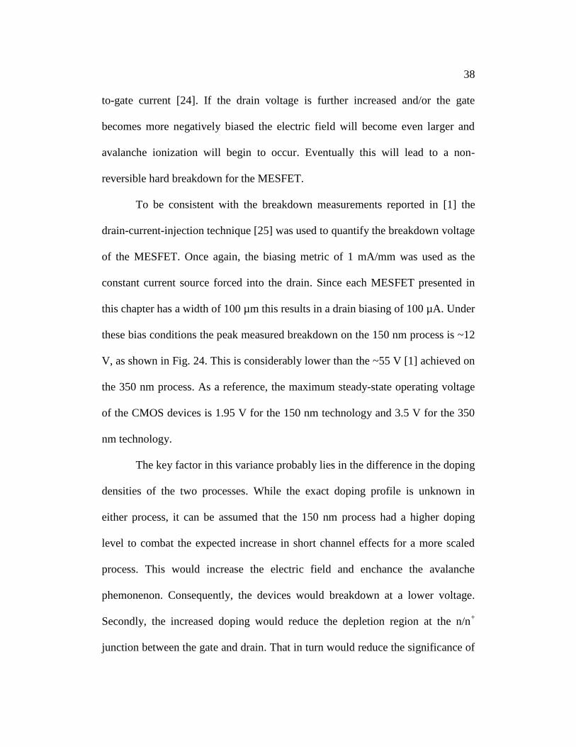
38
to-gate current [24]. If the drain voltage is further increased and/or the gate
becomes more negatively biased the electric field will become even larger and
avalanche ionization will begin to occur. Eventually this will lead to a non-
reversible hard breakdown for the MESFET.
To be consistent with the breakdown measurements reported in [1] the
drain-current-injection technique [25] was used to quantify the breakdown voltage
of the MESFET. Once again, the biasing metric of 1 mA/mm was used as the
constant current source forced into the drain. Since each MESFET presented in
this chapter has a width of 100 µm this results in a drain biasing of 100 µA. Under
these bias conditions the peak measured breakdown on the 150 nm process is ~12
V, as shown in Fig. 24. This is considerably lower than the ~55 V [1] achieved on
the 350 nm process. As a reference, the maximum steady-state operating voltage
of the CMOS devices is 1.95 V for the 150 nm technology and 3.5 V for the 350
nm technology.
The key factor in this variance probably lies in the difference in the doping
densities of the two processes. While the exact doping profile is unknown in
either process, it can be assumed that the 150 nm process had a higher doping
level to combat the expected increase in short channel effects for a more scaled
process. This would increase the electric field and enchance the avalanche
phemonenon. Consequently, the devices would breakdown at a lower voltage.
Secondly, the increased doping would reduce the depletion region at the n/n+
junction between the gate and drain. That in turn would reduce the significance of

39
increasing LaD which helps reduce the electric field at that junction and increase
the point at which the device breaks down. In any process though, LaD can only be
increased so much before it no longer has an effect. In the 350 nm technology this
roll-off occurs around LaD = 5 µm [1] compared to the LaD ~1 µm in the 150 nm
process. Without the positive impact of LaD beyond 1 µm, the 150 nm process
cannot be expected to reach breakdown voltages anywhere close to the 350 nm
process. For devices with LaD ≤ 1 µm it is expected that the breakdown voltage
would only be moderately reduced by the higher doping. This is exactly what was
observed in the measured results. Case in point, the MESFET with Lg = LaS = LaD
= 600 nm is ~8 V in the 150 nm process which is only a 4 V reduction from the
350 nm process [1].
It had been suggested in previous works [1-2] that the breakdown event
happened almost exclusively at the drain end and was independent of the access
region at the source side. Clearly this is not the case as shown in Fig. 24. The
breakdown is about twice as large with LaS = 600 nm as compared to LaS = 300
nm for Lg = 600 nm and LaD > 1 µm. Furthermore, for devices with LaS = 300 nm
the breakdown is essentially independent of LaD. This suggests that there is
another form of breakdown happening on the source side. Presumably the
breakdown event is not the result of tunneling/avalanche breakdown since the
electric field should be significantly lower as a result of the much smaller reverse
biasing at that junction. In the worst case scenario the reverse bias would not
exceed 1 to 1.5 V, whereas, on the drain side it will be 3.5 to 6 V. Thus, there

40
must be a critical length for LaS greater than 300 nm, but less than 600 nm on the
150 nm process in which this new breakdown is no longer an issue. This issue
was previously unseen before in other process runs since the lithography rules
prevented the width of the spacers from being reduced below 600 nm. Since there
are no devices with LaS other than 260, 300 and 600 nm there is insufficient data
to confirm this assumption.
0
2
4
6
8
10
12
14
0 1 2 3 4 5
Lg
= LaS
= 600 nm
Lg
= 400 nm, LaS
= 600 nm
Lg
= 600 nm, LaS
= 300 nm
Lg
= LaS
= 300 nm
Lg
= 150 nm, LaS
= 300 nmVo
ltag
e B
rea
kd
ow
n,
VB
D (
V)
Drain Access Length, LaD
(m)
Fig. 24. Shows the breakdown voltage of various MESFET
structures on the 150 nm SOI CMOS process.
To demonstrate the trade-off between current drive, breakdown voltage
and RF performance we plot the family of curves for drain voltages up to 10 V for
a device with Lg = 400 nm, LaS = 600 nm and LaD =1.0 µm in Fig. 25. This device
is similar to the one used for Fig. 17d but the longer LaS and LaD gives it a higher
breakdown voltage of ~11.5 V. Although the device has soft output saturation at
41
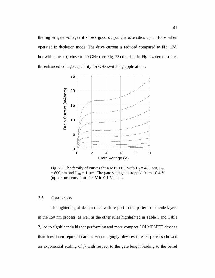
the higher gate voltages it shows good output characteristics up to 10 V when
operated in depletion mode. The drive current is reduced compared to Fig. 17d,
but with a peak fT close to 20 GHz (see Fig. 23) the data in Fig. 24 demonstrates
the enhanced voltage capability for GHz switching applications.
Fig. 25. The family of curves for a MESFET with Lg = 400 nm, LaS
= 600 nm and LaD = 1 µm. The gate voltage is stepped from +0.4 V
(uppermost curve) to -0.4 V in 0.1 V steps.
2.5. CONCLUSION
The tightening of design rules with respect to the patterned silicide layers
in the 150 nm process, as well as the other rules highlighted in Table 1 and Table
2, led to significantly higher performing and more compact SOI MESFET devices
than have been reported earlier. Encouragingly, devices in each process showed
an exponential scaling of fT with respect to the gate length leading to the belief
0
5
10
15
20
25
0 2 4 6 8 10
Dra
in C
urr
ent (m
A/m
m)
Drain Voltage (V)

42
that > 100 GHz MESFETs might be possible at the next technology node.
However it was shown that as MESFET gate lengths approach the limit of the
technology node they become strongly affected by short channel effects. Thus the
the future of MESFET scaling will depend largely on how the the width of the
spacers and BEOL rules scale. If they continue to scale well, very high fT
MESFETs could be achieved with slightly larger gate lengths, mitigating some of
the short channel effects. Granted, decreasing LaS or LaD will lower the breakdown
voltage, but it is expected that these devices will nevertheless have breakdown
voltages significantly higher than MOSFETs on the same process. Taking into
account all the various metrics for DC and RF performance, the best all around
device on this 150 nm process run would probably feature a gate length in the
range of 200-300 nm.
Before declaring that, it is important to note there was a second fabrication
run on the 150 nm process in which the focus was designing a very large
MEFSET device for an LDO application (further details and measurements from
that device are discussed in Chapter 5). Additionally a few other MESFETs
including BT-MESFETs with gate lengths of 250 and 300 nm and widths of 100
µm were added to monitor the run-to-run variations as well as to figure out the
optimum gate length. Unbeknowst to us at the time of the second fabrication,
Honeywell changed the silicide step to be slightly thinner in an effort to enhance
the performance of the MOSFETs. Consequently the thin silicon layer above the
buried oxide was left about 20 nm thicker and resulted in a negative shift in the

43
threshold voltage; as seen in Fig. 26. This change can be expected since a larger
negative voltage should now be needed at the gate-source junction to pinch off the
thicker channel. If Honeywell decides to keep the thinner silicide step for this
process, which it does appear to, then the ideal gate length for the MESFETs to
avoid excessive short channel effects while maintaining high performance will be
about 300 nm.
10-13
10-11
10-9
10-7
10-5
10-3
-1.5 -1 -0.5 0 0.5 1
Curr
ent (A
)
Gate Voltage (V)
VD = 25 mV
August 2008
May 2009
LaS
= LaD
= Lg = 300 nm
W = 100 m
Fig. 26. Comparison of Gummel plots for nominally identical Lg =
300 nm devices fabricated on the 150 nm process in August 2008
and May 2009.

44
CHAPTER 3
FD-SOI & SOS MESFETS
While FD-SOI CMOS products are in the minority compared to those in
traditional bulk or PD-CMOS processes it is used in many current applications
due to its superior low power capability. In the future though, it is almost a
certainty that FD-CMOS will gain in popularity since the thin silicon above the
insulator has been trending downwards with each progressive process node. This
scaling might ultimately lead to FD-CMOS supplanting PD-CMOS as an option
all together. Furthermore, it is also a certainty that a high voltage transistor will be
needed on those processes if certain analog applications are to be incorporated
since state-of-the-art processes already have breakdown voltages < 1 V. This
chapter proposes high voltage FD-MESFETs with breakdown voltages > 17 V
developed on commercial SOS and SOI CMOS processes aimed to fix this issue.
Additionally it will highlight some of the fundamental differences in operation
and layout from the PD-MESFETs.
3.1. FD-MESFET ARCHITECTURE
The FD-MESFET bases its basic design structure after the PD-MESFET
and has a similar fabrication flow as Fig. 2. Like the PD-MESFET, the Schottky
gate of the FD-MESFET is formed from the CoSi2 silicide layer in a lightly doped
n-well resulting in nearly ideal Schottky diode behavior. The key process step
once again is the patterning of the silicide block layer to form SiO2 spacers

45
between the contacts of the drain, gate, and source. Lastly, the critical access
length is at the drain (LaD) and is one the primary reasons for the MESFET’s high
breakdown capability.
The fundamental difference between the two types of MESFETs is how
the gate is oriented to conduct current. For PD-MESFETs, the silicon layer above
the insulator is 140-200 nm thick. In the creation of the Schottky gate, only about
30-100 nm of that silicon is consumed in the formation of the metal silicide. The
remaining silicon under the gate is sufficient enough to form a channel directly
under the gate. On the other hand, for FD-MESFETs the silicon layer above the
insulator is 50 nm or less. Most of this is then consumed during the formation of
the silicide. Any remaining silicon under the Schottky gate is too thin to form the
channel of the MESFET even under enhancement conditions because the forward
bias required to turn on the device would lead to excessive gate conduction. As a
result, conduction of the drain current does not occur directly under the gate.
Instead the layout is slightly altered, as depicted in Fig. 27 and Fig. 28, to confine
the current between islands of silicide that deplete the conducting channel in the
lateral direction. The definitions of LaS, LaD, and Lg remain the same as the PD-
MESFET. The new parameter of channel width denoted as LCW is introduced and
is the distance between the silicide islands. It is patterned in the same manner as
LaS and LaD. Generally speaking, the current drive of the device will increase with
an increase in LCW [26-27].

46
Fig. 27. 3-D rendering of the FD-SOI MESFET showing two
conducting channels confined between islands of silicide.
Electrical contact to each silicide island is provided by contacts to
the first layer of metal interconnect (not shown) [27].
Fig. 28. Shows a cross-section in the y-z plane through the center
of the device. The conducting channels are formed underneath the
regions of silicide block. The current flows into the channels as
indicated in the figure [27].
The FD-MESFETs were first fabricated on Peregrine’s 0.25 µm SOS
CMOS process and then on a 0.2 µm SOI CMOS process from MIT-Lincoln Labs
(MIT-LL). Using the standard FD layout shown in Fig. 27, the minimum feature
Insulator
Source DrainSilicide
BlockGate
Thin Silicon
Layer
Lcw
Lg
Silicide
Lcw
z
y
x
z
y

47
sizes of the Peregrine technology limited the minimum channel lengths and
widths to 1.8 µm and 0.25 µm respectively. The Lg limitation was the result of the
large contact size as well as the spacing requirement between the contact and the
silicide block layer. The PD-MESFET can overcome this layout limitation by
simply adopting the Fig. 12 orientation and making the gate contact at the top
and/or bottom of the device. In those devices the limitation then becomes the
minimum separation of the silicide block. FD devices with multiple channels on a
single finger conversely do not have a continuous gate. The gate between two
adjacent channels is isolated from the gate between any other set of channels.
Thus, a contact between each set of channels to a common metal line down the
gate is needed for the gate to be at equal potential. Having multiple channels in a
single finger is critical in minimizing the layout area and maximizing the current
drive since each channel will only contribute a current in the few µA’s range.
Current per channel will be dependent on doping level, LCW, Lg and other process
parameters [26-27]. It is important to point out that the backend metals of the
Peregrine process were that of a 0.6 µm process. If the Peregrine’s backend
metals were scaled to that of a typical 0.25 µm process the gate length using the
Fig. 27 structure would no longer be limited by the contact size and contact to
silicide block spacing but by the 1.2 µm minimum spacing of the silicide block.
MIT-LL’s more stringent handle on process features allowed for gate
lengths as small as 0.6 µm and channel widths of 0.2 µm with a layout similar to
Fig. 27. The core objective for the SOS MESFETs was to gather an understanding

48
on the effects parameters such as doping concentration, LCW, LaS, and LaD had on
threshold voltage, leakage current, breakdown voltage, and current drive. On the
ensuing run with MIT-LL, the most successful structures from the SOS MESFETs
were then transferred over to equivalent SOI MESFET structures with smaller
gate lengths and placed in GSG structures for high frequency parameter
extraction. The amount of layout area dedicated to testing RF performance was
limited for the Peregrine process since it would be admittedly poor with the large
gate lengths. In both processes, each MESFET was designed to have multiple
fingers having a number of nominally identical channels.
The ease of being able to control the threshold voltage is a distinct
advantage of FD-MESFETs. Threshold voltage is dependent upon the separation
of the silicide islands. For n-channel devices, the larger the separation, the more
negative the threshold becomes due to the increased distance that needs to be
overcome to fully deplete the channel and pinch it off. A comparable reasoning
can be used to describe p-channel devices, except their threshold becomes more
positive with increased separation. This is analogous to PD-MESFETs whose
thresholds are directly related to vertical thickness of the channel. Vertical
thickness however is not a parameter that can be changed without changing the
CMOS process flow. Similarly, altering the doping concentration can be used to
change the threshold but it also comes at the cost of changing the process flow
[27].

49
Fig. 29 shows the threshold versus the channel width for both n-type and
p-type devices on a FD-SOS MESFET process. Based on the linear fits which are
represented by the dashed lines, it can be found that the threshold varies as -0.11
V/µm for n-MESFETs and +0.07 V/µm for p-MESFETs. Presumably the
difference can be explained by the heavier doping in the n-well as compared to
the p-well. These results suggest that complementary MESFET operation (i.e. Vtn
= -Vtp with similar saturated drain currents) could be achieved by optimizing the
n- and p-well implants and the channel widths LCWN and LCW
P, although that
would require changes to the CMOS process flow itself as well [27].
Fig. 29. Threshold voltage of SOS MESFETs as a function of the
channel width. The dashed lines are linear fits to the data [27].
3.2. REGIONS OF DEVICE OPERATION
The regions of operation for this MESFET are illustrated by Fig. 30-Fig.
32. Fig. 30 is composed of 2-D drawings that show the lateral depletion growth
-0.78
-0.76
-0.74
-0.72
-0.70
-0.68
-0.66
0.25
0.30
0.35
0.40
0.45
0.50
0.55
0 1 2 3
N-M
ES
FE
T, V
th (
V) P
-ME
SF
ET
, Vth (V
)
LCW
(m)

50
along a cross-section in the y-z plane as it expands from the edges of the silicide
islands controlled by the gate. While the pinching off of the channel happens in
the lateral direction, the depletion region will be unequal from the drain to the
source as was the case for PD-MESFETs. Once again, above a few 10’s of mV
the depletion region will begin to favor the drain side of the device. Thus, Fig. 30
by itself is insufficient in describing the operation of FD-MESFET. Fig. 31
completes the description of the FD-MESFET with diagrams depicting the
depletion region in a simplified top level view. This section is more or less a
repeat of Section 1.3; nevertheless, due to the slight differences of the devices and
depletion region growth in two planes it is useful to repeat.
At very low drain voltages and assuming VGS > Vt, a current begins to
flow in the channel created under LCW. The depletion region starts to build up
evenly along the silicide islands from the drain to the source. An electric field is
established across the channel, resulting in a current flow that varies linearly with
drain voltage. In this region of operation the channel operates as a resistor. The
junction between the drain and the gate becomes more reversed biased with
increasing drain voltage leading to the depletion region widening faster towards
the drain side. The narrowing of the channel at the drain end leads to a decrease in
the slope of ID and the rounding off effect shown in Fig. 32 [14]. At a certain
drain voltage the depletion width from each side of the silicide island touches and
the channel becomes pinched off. Presumably, the pinch-off point will be closer
to the drain side of the device. The region above the pinch-off point is the

51
saturation region. Theoretically, the slope of ID becomes zero and the drain
current becomes independent to further increases in drain voltage. Realistically,
this is not the case due to channel length modulation effects. When VGS becomes
more negative the depletion width will see an increase due to the junction
becoming more reversed biased. The reduced channel region leads to smaller
slopes of ID in the linear region; hence it is more resistive and pinches-off at lower
drain voltages. Below VGS < Vt, the channel becomes fully depleted and enters the
subthreshold region. In this region small amounts of current flow still flow due to
the diffusion of carriers in the space charge region [10].

52
Fig. 30. Lateral depletion for various regions of device operation.
a) VGS = 0 V and VDS = 0 V. b) Linear region: VGS = 0 V and small
VDS. c) Pinch-off: VGS = 0 V and VDS = VDSAT. d) Saturation
region: VGS = 0 V and VDS > VDSAT. e) Subthreshold region: VGS <
Vt and VDS = 0 V.
LCWLCW
Insulator
Depletion Layer
LCWLCW
Insulator
Depletion Layer
LCWLCW
Insulator
Depletion Layer
LCWLCW
Insulator
Depletion Layer
LCWLCW
Insulator
Depletion Layer
b)
c)
d)
a)
e)
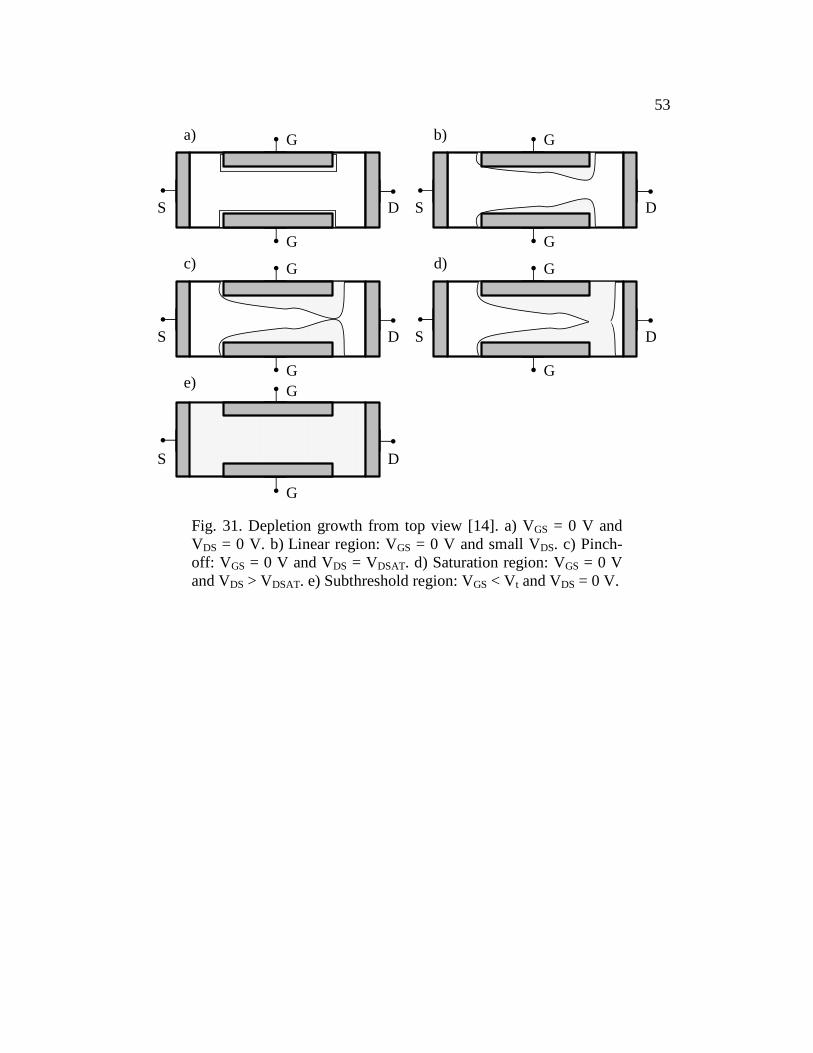
53
Fig. 31. Depletion growth from top view [14]. a) VGS = 0 V and
VDS = 0 V. b) Linear region: VGS = 0 V and small VDS. c) Pinch-
off: VGS = 0 V and VDS = VDSAT. d) Saturation region: VGS = 0 V
and VDS > VDSAT. e) Subthreshold region: VGS < Vt and VDS = 0 V.
G
G
DS
G
G
DS
G
DS
G
G
DS
G
G
S
G
D
a) b)
c)
e)
d)
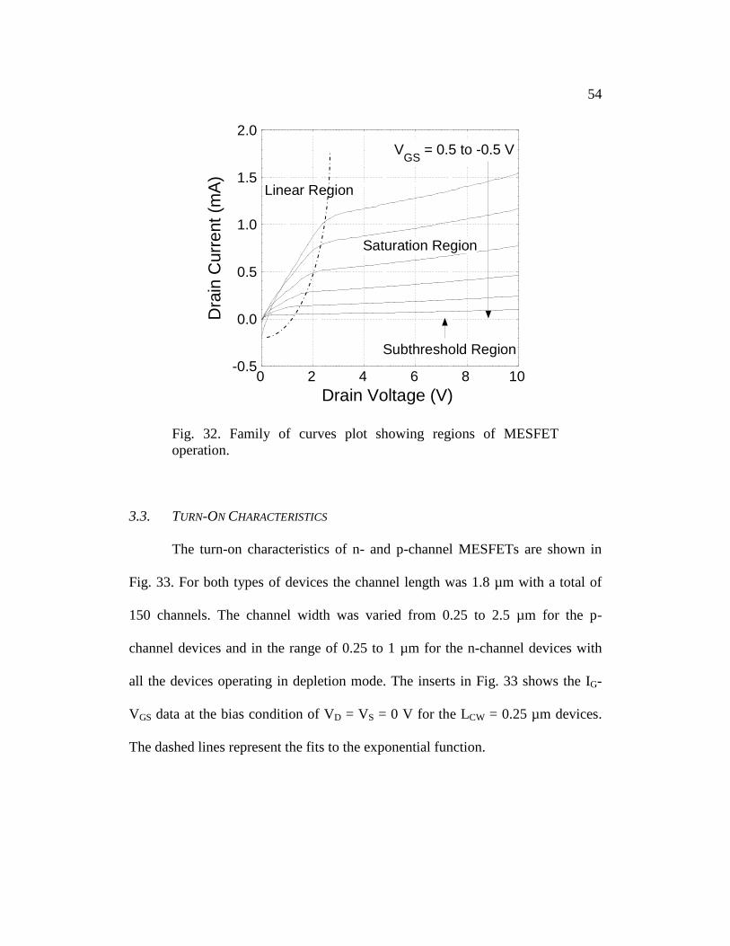
54
-0.5
0.0
0.5
1.0
1.5
2.0
0 2 4 6 8 10
Dra
in C
urr
ent
(mA
)
Drain Voltage (V)
Linear Region
VGS
= 0.5 to -0.5 V
Saturation Region
Subthreshold Region
Fig. 32. Family of curves plot showing regions of MESFET
operation.
3.3. TURN-ON CHARACTERISTICS
The turn-on characteristics of n- and p-channel MESFETs are shown in
Fig. 33. For both types of devices the channel length was 1.8 µm with a total of
150 channels. The channel width was varied from 0.25 to 2.5 µm for the p-
channel devices and in the range of 0.25 to 1 µm for the n-channel devices with
all the devices operating in depletion mode. The inserts in Fig. 33 shows the IG-
VGS data at the bias condition of VD = VS = 0 V for the LCW = 0.25 µm devices.
The dashed lines represent the fits to the exponential function.
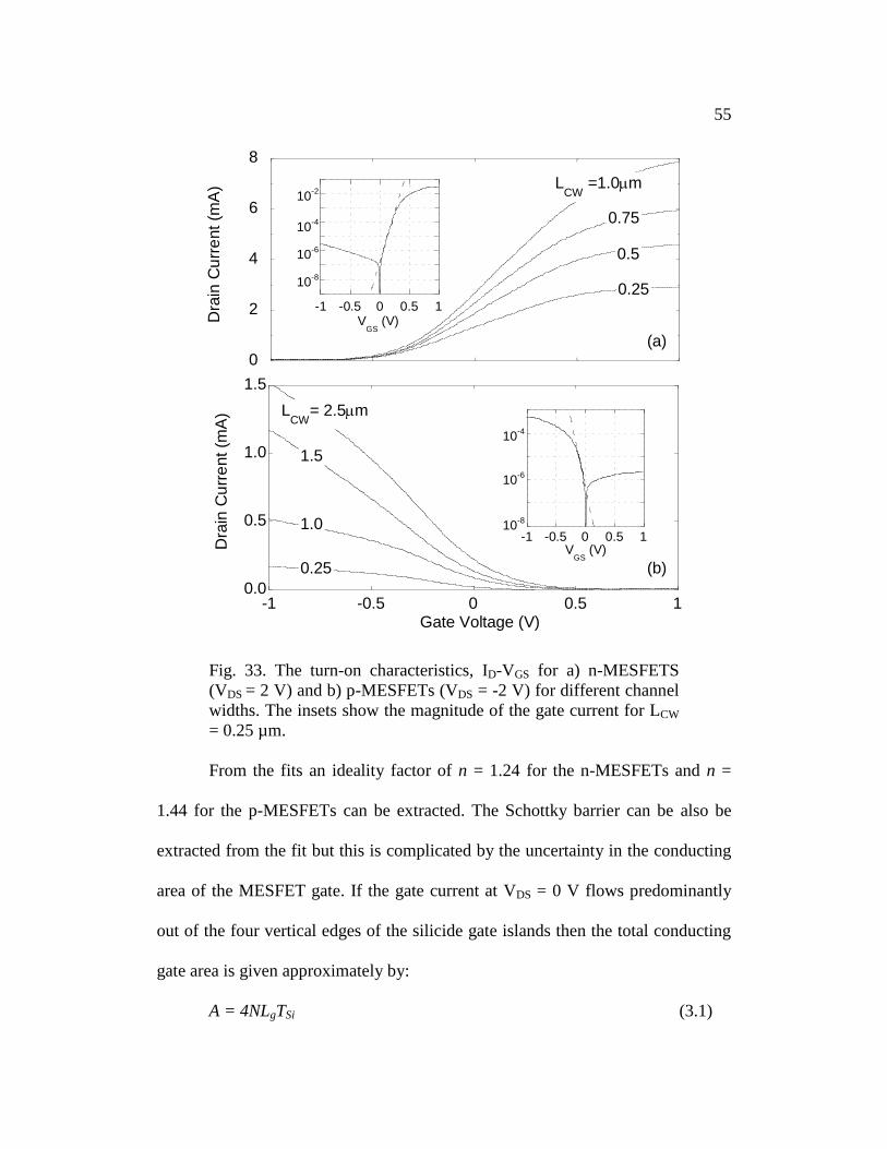
55
Fig. 33. The turn-on characteristics, ID-VGS for a) n-MESFETS
(VDS = 2 V) and b) p-MESFETs (VDS = -2 V) for different channel
widths. The insets show the magnitude of the gate current for LCW
= 0.25 µm.
From the fits an ideality factor of n = 1.24 for the n-MESFETs and n =
1.44 for the p-MESFETs can be extracted. The Schottky barrier can be also be
extracted from the fit but this is complicated by the uncertainty in the conducting
area of the MESFET gate. If the gate current at VDS = 0 V flows predominantly
out of the four vertical edges of the silicide gate islands then the total conducting
gate area is given approximately by:
A = 4NLgTSi (3.1)
0
2
4
6
8
LCW
=1.0m
0.75
0.5
Dra
in C
urr
ent (m
A)
0.25
0.0
0.5
1.0
1.5
-1 -0.5 0 0.5 1
Dra
in C
urr
ent (m
A)
Gate Voltage (V)
LCW
= 2.5m
1.5
1.0
0.25
-1 -0.5 0 0.5 1V
GS (V)
10-2
10-4
10-6
10-8
-1 -0.5 0 0.5 1V
GS (V)
10-4
10-6
10-8
(a)
(b)

56
where
N = number of channels
TSi = thickness of Si channel.
For the SOS devices, TSi ≈ 100 nm [28] and the total gate area is ~1.1x10⁻⁶
cm2 for the devices with N = 150 channels. Assuming effective Richardson
constants of 110 and 32 A·cm-2
·K-2
[29], Equation 1.5 can be used to derive
barrier heights of 0.48 and 0.41 eV respectively for the n- and p-channel
MESFETs. The measured barrier height for the p-type MESFETs is in good
agreement with the ~0.4 eV quoted in the literature for CoSi2 on p-Si [30]. The
value for the n-MESFETs is lower than the ~0.6 eV quoted for CoSi2 on n-Si but
is still reasonable given the uncertainty in the gate area.
3.4. BREAKDOWN MECHANISMS
The breakdown of the 0.25 µm FD-SOI CMOS was only 3.5 V which can
be insufficient for certain analog circuit applications. In this same process,
MESFETs with breakdowns exceeding 17 V were readily available without
altering any of the process steps. Fig. 34a and b shows the family of curves plot
for n-channel and p-channel devices which exhibited good output current
saturation at drain voltages that greatly exceeded the CMOS breakdown. As was
the case with PD-MESFETs, the high voltage capability of the FD-MESFETs is
in large part due to the drift region between the ends of the channel and the drain
contact and is a natural outcome of the non self-aligned MESFET geometry [1].
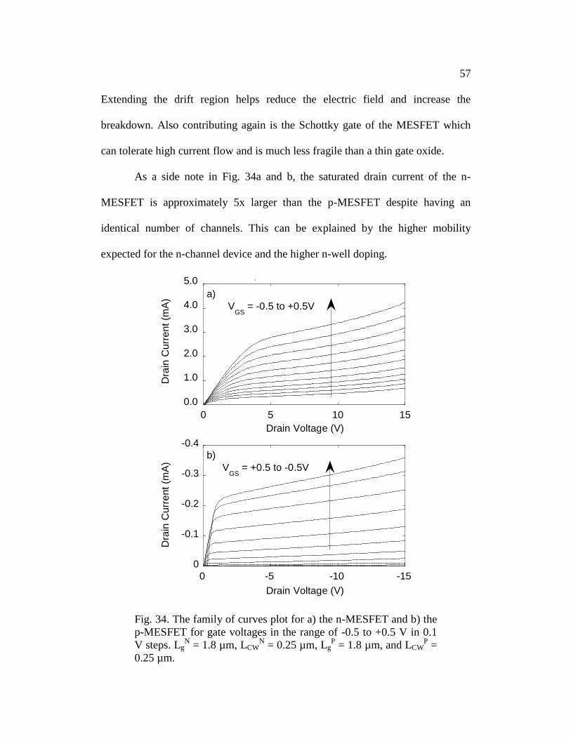
57
Extending the drift region helps reduce the electric field and increase the
breakdown. Also contributing again is the Schottky gate of the MESFET which
can tolerate high current flow and is much less fragile than a thin gate oxide.
As a side note in Fig. 34a and b, the saturated drain current of the n-
MESFET is approximately 5x larger than the p-MESFET despite having an
identical number of channels. This can be explained by the higher mobility
expected for the n-channel device and the higher n-well doping.
Fig. 34. The family of curves plot for a) the n-MESFET and b) the
p-MESFET for gate voltages in the range of -0.5 to +0.5 V in 0.1
V steps. LgN = 1.8 µm, LCW
N = 0.25 µm, Lg
P = 1.8 µm, and LCW
P =
0.25 µm.
-0.4
-0.3
-0.2
-0.1
0
-15-10-50
Dra
in C
urr
ent
(mA
)
Drain Voltage (V)
VGS
= +0.5 to -0.5V
b)
0.0
1.0
2.0
3.0
4.0
5.0
0 5 10 15
Dra
in C
urr
ent
(mA
)
Drain Voltage (V)
VGS
= -0.5 to +0.5V
a)

58
In order to reduce layout area and improve RF performance, polysilicon
(poly) can be used to create the access region at the source. The access region
created using the polysilicon is similar to a gate of MOSFET and will prevent the
silicide step in the CMOS process from shorting the source to the gate. In the 0.25
µm FD-SOI CMOS process, the polysilicon can be patterned to be as small as
0.25 µm compared to 1.2 µm required for the silicide block. Polysilicon does
break down at lower voltages then silicide block, but with the majority of the
breakdown event taking place at the drain end, polysilicon can be substituted at
the source end without dramatically affecting the breakdown of the device.
Doping levels can also alter the breakdown of the device. Similar to the
case of MOSFETs, a higher doping implant will reduce the MESFETs depletion
region at the n/n+ junction from the gate to drain and reduce the breakdown of the
device. In the Peregrine process, there were three different doping profiles
available with the intention of having low and high threshold devices to go along
with their standard PMOS and NMOS devices. Unfortunately, there was not a set
of three MESFETs layouts with the exact same geometries with only the doping
profile differing to physically test this theory. There is however two devices that
can be compared, one with the standard implant and one with the heavy implant
used for high threshold MOSFETs. Both MESFETs feature 150 channels, LCW =
0.25 µm, Lg = 0.6 µm, LaS = 0.6 µm (poly) and LaD = 1.2 µm (SB). The device
with the standard doping had a breakdown voltage of about 16 V while the high
implant device was only 10.5 V. The breakdown was once again determined by
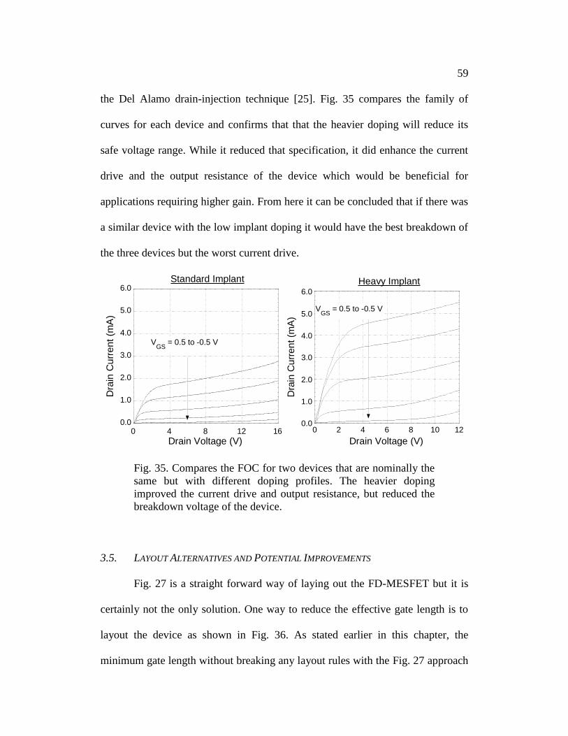
59
the Del Alamo drain-injection technique [25]. Fig. 35 compares the family of
curves for each device and confirms that that the heavier doping will reduce its
safe voltage range. While it reduced that specification, it did enhance the current
drive and the output resistance of the device which would be beneficial for
applications requiring higher gain. From here it can be concluded that if there was
a similar device with the low implant doping it would have the best breakdown of
the three devices but the worst current drive.
0.0
1.0
2.0
3.0
4.0
5.0
6.0
0 4 8 12 16
Dra
in C
urr
en
t (m
A)
Drain Voltage (V)
Standard Implant
VGS
= 0.5 to -0.5 V
0.0
1.0
2.0
3.0
4.0
5.0
6.0
0 2 4 6 8 10 12
Heavy ImplantD
rain
Cu
rre
nt (m
A)
Drain Voltage (V)
VGS
= 0.5 to -0.5 V
Fig. 35. Compares the FOC for two devices that are nominally the
same but with different doping profiles. The heavier doping
improved the current drive and output resistance, but reduced the
breakdown voltage of the device.
3.5. LAYOUT ALTERNATIVES AND POTENTIAL IMPROVEMENTS
Fig. 27 is a straight forward way of laying out the FD-MESFET but it is
certainly not the only solution. One way to reduce the effective gate length is to
layout the device as shown in Fig. 36. As stated earlier in this chapter, the
minimum gate length without breaking any layout rules with the Fig. 27 approach
60
is 1.8 µm. For the 0.25 µm FD-SOI CMOS process, 1.8 µm is not the minimum
distance of poly to poly, SB to SB or even poly to SB. Therefore by extending the
poly or SB used to create the access regions into the gate region the effective gate
length can be reduced to 0.6 µm. Fig. 37a shows the improvement when the gate
length is reduced from 1.8 µm to 0.6 µm for two devices that are nominally the
same with respect to every other parameter including doping profile, number of
channels, LCW, LaS and LaD. These results however are slightly misleading due to
the increased die area required to layout the structure in Fig. 36. There is a
minimum width for both the poly and silicide block which is considerably larger
than LCW and the minimum distance between the contact and those two layers still
needs to stay intact in order to not break design rules. Table 3 compares the area
consumed by the two devices in Fig. 37a. Fig. 37b normalizes the data by
showing current drive per unit area so that the two devices can be accurately
compared. While the normalization has dampened some of the apparent current
drive improvement, it can be expected that this device with an Lg = 0.6 µm will
have a much more favorable RF performance. Additionally, these devices have a
gate leakage current that is close to 3x less. This corresponds to the gate length
which is one-third the size.

61
Insulator
Source Drain
Silicide
Block
Thin Silicon
Layer
Lcw
Gate
Lg
Lcw
Fig. 36. 3-D rendering a FD-MESFET which extends silicide block
into the gate region to reduce the effective gate length.
10-8
10-7
10-6
10-5
10-4
10-3
10-2
10-1
-1.5 -1 -0.5 0 0.5 1
Cu
rre
nt
(A)
Gate Voltage (V)
VD = 2 V
LCW
= 0.25 m
LaS
= 0.6 m
LaD
= 1.2 m
150 Channels
Lg = 0.6 m
Lg = 1.8 m
10-6
10-5
10-4
10-3
10-2
10-1
100
101
-1.5 -1 -0.5 0 0.5 1
Cu
rre
nt
(A/m
m2)
Gate Voltage (V)
LCW
= 0.25 m
LaS
= 0.6 m
LaD
= 1.2 m
150 Channels
Lg = 0.6 m
Lg = 1.8 m
VD = 2 V
Fig. 37. a) Compares two devices, that are nominally similar
expect one utilizes the structure in Fig. 27 (Lg = 1.8 µm--solid line)
and the other uses Fig. 36 (Lg =0.6 µm--dashed line). b) Compares
the two devices after they have been normalized to current per unit
area.
z
y
x
a) b)

62
Table 3: Area of MESFETs in Fig. 37a
Layout Structure Area
Fig. 27 18.6 x 138 µm
Fig. 36 24.3 x 138 µm
Another possible architecture is shown in Fig. 38. This device is a
combination of the ideas presented in Fig. 27 and Fig. 36. The basic principle is to
extend the polysilicon or silicide block from the access region into gate region
like in Fig. 36. Unlike Fig. 36 which put the extended pieces of the access region
directly across from each other, this device offsets them. The effective gate length
is now the distance between the pieces and can now be made less than 0.6 µm
without breaking any layout rules. Theoretically this distance can approach zero,
however as shown in Fig. 39, there is a limit to how much the effective gate
length can be reduced. The devices in Fig. 39 are from the MIT-LL process since
there was not a complete set of devices to compare on the Peregrine process.
Nevertheless, the concept will still be the same. By offsetting the gate by half in
Fig. 39a, a significant increase in drive current can be seen. While the threshold
becomes more negative, the device still shows enough gate control to be useful in
different circuit applications. The device designed with a full offset and
theoretical Lg = 0 µm further increases the current drive but shows very little gate
control and does not really ever shutoff. As was the case with Fig. 36, this layout
will increase the die area slightly; refer to Table 4 for the different sizes. For each
finger, the length in the x-direction would increase by the length of the added

63
access region. The rest of the dimensions would be the same as in Fig. 27. In
devices with several channels per finger this device would have a smaller layout
area than the one in Fig. 36.
Insulator
SourceGate
DrainSilicide
Block
Thin Silicon
Layer
LcwLg
Fig. 38. 3-D rendering of a FD-MESFET showing silicide block
being offset in order to reduce the effective gate length.
10-9
10-8
10-7
10-6
10-5
10-4
-1.5 -1 -0.5 0 0.5 1
Cu
rre
nt
(A)
Gate Voltage (V)
No Offset
Half Offset
Full Offset
VD = 2 V
Lg = 0.8 m
LCW
= 0.2 m
LaS
= LaD
= 0.5 m
1 Channel 10
-4
10-3
10-2
10-1
100
101
-1.5 -1 -0.5 0 0.5 1
Curr
ent (A
/mm
2)
Gate Voltage (V)
No Offset
Half Offset
Full Offset
VD = 2 V
Lg = 0.8 m
LCW
= 0.2 m
LaS
= LaD
= 0.5 m
1 Channel
Fig. 39. a) Compares the Gummel plots of three devices with
different gate offsets on the MIT-LL process. b) Compares the
same devices after they have been normalized to current per unit
area.
z y
x
a) b)
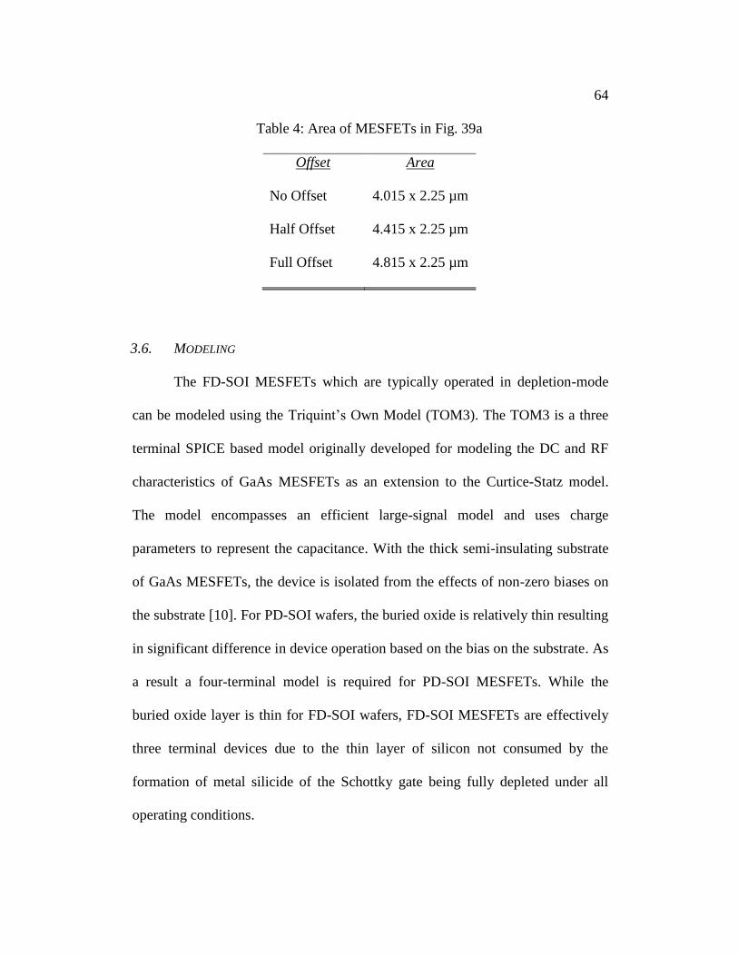
64
Table 4: Area of MESFETs in Fig. 39a
Offset Area
No Offset 4.015 x 2.25 µm
Half Offset 4.415 x 2.25 µm
Full Offset 4.815 x 2.25 µm
3.6. MODELING
The FD-SOI MESFETs which are typically operated in depletion-mode
can be modeled using the Triquint’s Own Model (TOM3). The TOM3 is a three
terminal SPICE based model originally developed for modeling the DC and RF
characteristics of GaAs MESFETs as an extension to the Curtice-Statz model.
The model encompasses an efficient large-signal model and uses charge
parameters to represent the capacitance. With the thick semi-insulating substrate
of GaAs MESFETs, the device is isolated from the effects of non-zero biases on
the substrate [10]. For PD-SOI wafers, the buried oxide is relatively thin resulting
in significant difference in device operation based on the bias on the substrate. As
a result a four-terminal model is required for PD-SOI MESFETs. While the
buried oxide layer is thin for FD-SOI wafers, FD-SOI MESFETs are effectively
three terminal devices due to the thin layer of silicon not consumed by the
formation of metal silicide of the Schottky gate being fully depleted under all
operating conditions.

65
The TOM3 model itself though is insufficient in modeling the FD-SOI
MESFET’s soft and hard breakdown. Furthermore, the model has trouble
matching the slope of the gate leakage current in the reverse biased region of the
curve. If Cadence [31] is being used to simulate the circuit, there is an option in
the Analog Design Environment under Simulation Options Analog which
has the parameter gmin that can be adjusted to model the slope of the leakage
current (Fig. 40). This method is only effective if the circuit being design is
comprised of only MESFETs since gmin is also is common to the MOSFETs and
will affect their operation. A better solution is to use the diode sub-circuits,
marked by IBDS and IBGD in Fig. 41 which can be used to model both the
breakdown and the reverse gate leakage.
Fig. 40. Screen shot of how to change gmin in Cadence’s Analog
Design Environment.

66
Fig. 41. Large signal model of a MESFET with the TOM3 sub-
circuit. IBGD and IBDS are used to model the breakdown voltage in
the circuit [23].
Aside from the sub-circuit diodes, the MESFET TOM3 model consists of
parasitic resistances at the source (RS), gate (RG), and drain (RD), a voltage-
controlled current source (Ids), and a drain-to-source capacitor (Cds). The TOM3
model accounts for the gate-to-source capacitance, Cgs, in its charge based model
which is described in detail in [23, 32]. The model also includes circuitry to
model the drain dispersion and self-heating effects.
The modeling and extraction of FD-SOI MESFETs was based on an
approach developed by Balijepalli for PD-SOI MESFETs [10]. Using her method,
modeling of the DC operation was done for two different devices on the Peregrine
process. Fig. 42-Fig. 45 show the modeling for one of those devices. The device
features 300 channels, LCW = 0.25 µm, Lg = 1.8 µm, LaS = LaD = 1.2 µm (poly),
and the standard doping profile. In each figure the measured results are
represented by the solid line and the simulated model is shown by the open
circles.
Cds
RG
RS
RD
S
G Rds
Igs
Ild
Igd
Ils Ids
+
Vc
tGD
*1012
K?|V
C|
TOM3 SUB-CIRCUIT
DIBGD
IBDS

67
0
1
2
3
0 1 2 3 4
Dra
in C
urr
en
t (m
A)
Gate Voltage (V)
VGS
= 0.5 to -0.5 V_ Measured
o Simulated
Fig. 42. Compares the measured results (solid line) to the
simulated model (open circles) for the family of curves plot.
10-8
10-7
10-6
10-5
10-4
10-3
10-2
10-1
-1.5 -1 -0.5 0 0.5 1
Curr
ent (A
)
Gate Voltage (V)
VD
= 2 V
Fig. 43. Compares the Gummel plots of the measured results (solid
line) to the simulated model (open circles).
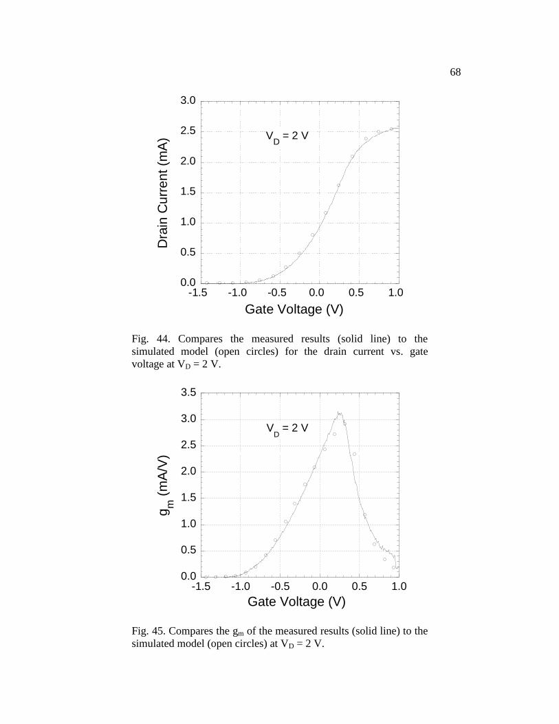
68
0.0
0.5
1.0
1.5
2.0
2.5
3.0
-1.5 -1.0 -0.5 0.0 0.5 1.0
Dra
in C
urr
en
t (m
A)
Gate Voltage (V)
VD
= 2 V
Fig. 44. Compares the measured results (solid line) to the
simulated model (open circles) for the drain current vs. gate
voltage at VD = 2 V.
0.0
0.5
1.0
1.5
2.0
2.5
3.0
3.5
-1.5 -1.0 -0.5 0.0 0.5 1.0
gm
(m
A/V
)
Gate Voltage (V)
VD = 2 V
Fig. 45. Compares the gm of the measured results (solid line) to the
simulated model (open circles) at VD = 2 V.
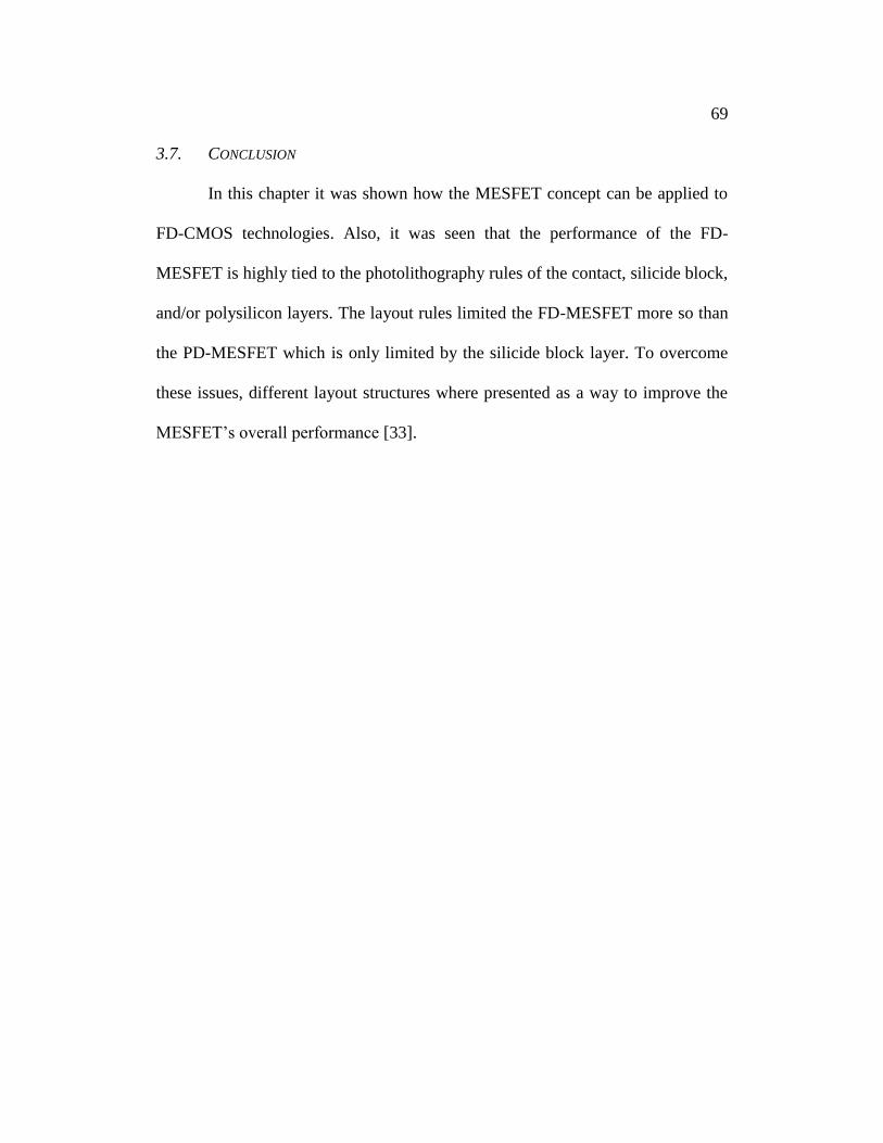
69
3.7. CONCLUSION
In this chapter it was shown how the MESFET concept can be applied to
FD-CMOS technologies. Also, it was seen that the performance of the FD-
MESFET is highly tied to the photolithography rules of the contact, silicide block,
and/or polysilicon layers. The layout rules limited the FD-MESFET more so than
the PD-MESFET which is only limited by the silicide block layer. To overcome
these issues, different layout structures where presented as a way to improve the
MESFET’s overall performance [33].
70
CHAPTER 4
N-MESFET LDO
One of the primary concerns and key selling point for battery powered
electronics is the design of the power management system. With consumer’s
continued expectation that products such as cell phones and laptops last longer
and longer without recharging, power management systems can ill afford to waste
any unnecessary power that will degrade battery lifetime and potential sales of the
product. As such, most complex systems incorporate several voltage regulators to
optimally supply the various components within the system. This as a result has
driven the market for ultra low dropout LDOs. These LDOs can feature extremely
high power efficiencies under certain line and load conditions.
LDOs are also particularly popular in applications that are sized
constrained and/or noise sensitive. Commercial LDOs are available in extremely
small packages and in general have superior noise performance and fewer
required external components than switching regulators. The MESFET based
LDO furthers this point by providing stable regulation independent of a charge
pump and load capacitor across all line and load conditions. Having no external
capacitance is particularly important in ultra-compact applications since the
capacitor can be close to the size of the LDO itself. Furthermore, if a capacitor is
present, additional real estate on the PCB board will be needed for added traces
and spacing between the two components. Having no output capacitor is also
important for system-on-chip designs since it will save the chip a pin that could be
used elsewhere.

71
This chapter presents an LDO that was fabricated on the same 0.25 µm
FD-SOS CMOS process discussed in Chapter 3 and is centered on a FD-MESFET
pass device. As mentioned in the previous chapters, MESFETs can be integrated
alongside the SOS CMOS devices at no additional cost or change to the process.
This enables designs to take advantage of both technologies and yield the highest
performance. The MESFET based LDO demonstrates this approach by
implementing the rest of the LDO minus the pass transistor with SOS CMOS
transistors.
4.1. PMOS LDO OVERVIEW
The most critical aspect of the LDO regulator design is in the
implementation of the pass transistor. The choice of the pass transistor affects the
LDO’s stability, dropout voltage, transient response, ground current, and almost
every other critical figure of merit. The most common implementation of LDOs
employs a PMOS device as the pass transistor in a common-source (CS)
configuration as shown in Fig. 46. The CS architecture is popular since it can
produce very low dropout voltages that are theoretically dependent only on the
on-resistance, Ron, of the pass transistor and the load current, Iload without a charge
pump (Equation 4.1). In reality though, the dropout voltage also must include the
parasitic voltage drops from the metal routing lines. These parasitic voltage drops
can become significant at higher load currents.
DSATloadonLDOPMOSDO VIRV )( (4.1)
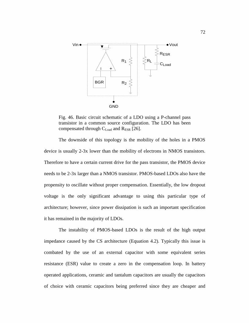
72
Fig. 46. Basic circuit schematic of a LDO using a P-channel pass
transistor in a common source configuration. The LDO has been
compensated through CLoad and RESR [26].
The downside of this topology is the mobility of the holes in a PMOS
device is usually 2-3x lower than the mobility of electrons in NMOS transistors.
Therefore to have a certain current drive for the pass transistor, the PMOS device
needs to be 2-3x larger than a NMOS transistor. PMOS-based LDOs also have the
propensity to oscillate without proper compensation. Essentially, the low dropout
voltage is the only significant advantage to using this particular type of
architecture; however, since power dissipation is such an important specification
it has remained in the majority of LDOs.
The instability of PMOS-based LDOs is the result of the high output
impedance caused by the CS architecture (Equation 4.2). Typically this issue is
combated by the use of an external capacitor with some equivalent series
resistance (ESR) value to create a zero in the compensation loop. In battery
operated applications, ceramic and tantalum capacitors are usually the capacitors
of choice with ceramic capacitors being preferred since they are cheaper and
+_
Vin Vout
GND
BGR
RLR1
R2
RESR
CLoad

73
come in small packages. For older LDOs, careful design was needed in choosing
an appropriate load capacitor. If the ESR value associated with the capacitor was
too small or too big, the LDO could oscillate. Companies simplified the process
slightly for end users by including figures in datasheets like the one in Fig. 47
[34]. From the figure, it be can be determined that this particular LDO with a 4.7
µF load capacitor needs an ESR value between 0.3 and 8 Ω across all loads to
guarantee stability. Based on that, a tantalum capacitor would probably be
recommended for the simplest solution since it usually encompasses an ESR
value that is not too high or too low as to cause instability. With a ceramic
capacitor on the other hand, an additional external series resistor might be needed
to meet the ESR requirement since they frequently have very low ESR values.
Several new LDOs are now being designed to be stable with little to no ESR. This
removes the previous concern with ceramics, but not the chief issue of needing an
external capacitor.
)(11)( //)//( pmosoLpmosoout rRRRrR (4.2)

74
Fig. 47. Range of stability chart for the Texas Instruments
TPS76301 LDO. CSR refers to the ESR from the capacitor plus
any external resistor if applicable [34].
Fig. 48 illustrates the key internal parasitic sources as well as the added
external components that affect the stability of the LDO system. Although it is not
shown in Fig. 46, it can be assumed that the error amplifier is a single stage, one
pole amplifier followed by a buffer. A buffer is needed to drive the large
capacitive impedance created by the very large pass device. With the buffer now
being accounted for, the corresponding close loop response is shown in Fig. 49.
The first pole, P1, (Equation 4.3) is determined by the load capacitor, CLoad, ESR
value, and the resistance at the LDO’s output which was found in Equation 4.2.
The combination of the output impedance of the error amplifier represented by
CO1 and RO1 and the input capacitance of the buffer, CI2, forms the second pole,
P2, (Equation 4.4). In Equation 4.4, the combination of CO1 and CI2 is represented
as Cpar1. Depending on the CLoad selection, design of the buffer, and size of pass

75
transistor, P1 and P2 can be reversed [35-37]. Nevertheless, they are usually found
at low frequencies. The placement of the zero, Z1, (Equation 4.5) is determined by
CLoad and its associated ESR. Lastly, P3, (Equation 4.6) is the combination of the
output resistance of the buffer, RO2, its capacitance, CO2, and the parasitic
capacitance of the pass transistor, Cpmos. The combination of CO2 and Cpmos is
represented by Cpar2 in Equation 4.6. Compensation is further complicated by the
fact that P1 will move under different load conditions with the worst case
occurring when the load current is at its highest [37]. At that point ro(pmos) and
consequently Rout is at its lowest which causes P1 and the gain bandwidth (GBW)
to be pushed to higher frequencies. This effect must be taken into account when
determining Z1 [35]. There are additional poles present in the LDO loop;
however, since they occur at frequencies much higher than the GBW they were
neglected from this discussion [36-37].
Vin
+
_
Vout
RL
R1
R2
RESR
CLoad
RO1 CO1 CI2 RO2 CO2 Cpmos
Error Amplifier Buffer
BGRro(pmos)
Fig. 48. Includes the key internal parasitic components as well as
the added external components that affect the stability of the
PMOS LDO system.

76
Fig. 49. Closed-loop gain response of a compensated LDO
utilizing a PMOS pass transistor.
)(2
11
ESRoutLoad
PRRC
f
(4.3)
11
22
1
Opar
PRC
f
(4.4)
ESRLoad
ZRC
f2
11
(4.5)
22
32
1
Opar
PRC
f
(4.6)
4.2. NMOS LDO OVERVIEW
NMOS (enhancement mode) linear regulators use the pass transistor of the
LDO in a common drain configuration (CD) as shown in Fig. 50. For stability
purposes, a CD configuration is highly desirable. By taking the output of the LDO
at the source of the pass transistor, the equivalent resistance at the output node
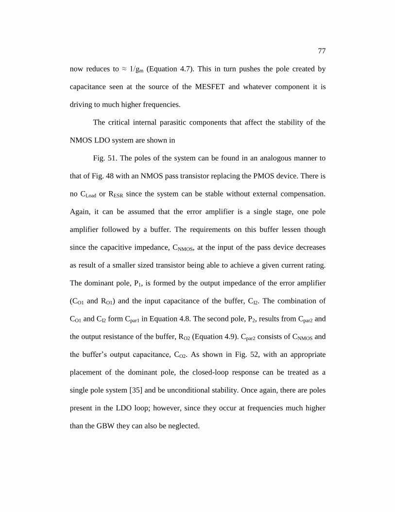
77
now reduces to ≈ 1/gm (Equation 4.7). This in turn pushes the pole created by
capacitance seen at the source of the MESFET and whatever component it is
driving to much higher frequencies.
The critical internal parasitic components that affect the stability of the
NMOS LDO system are shown in
Fig. 51. The poles of the system can be found in an analogous manner to
that of Fig. 48 with an NMOS pass transistor replacing the PMOS device. There is
no CLoad or RESR since the system can be stable without external compensation.
Again, it can be assumed that the error amplifier is a single stage, one pole
amplifier followed by a buffer. The requirements on this buffer lessen though
since the capacitive impedance, CNMOS, at the input of the pass device decreases
as result of a smaller sized transistor being able to achieve a given current rating.
The dominant pole, P1, is formed by the output impedance of the error amplifier
(CO1 and RO1) and the input capacitance of the buffer, CI2. The combination of
CO1 and CI2 form Cpar1 in Equation 4.8. The second pole, P2, results from Cpar2 and
the output resistance of the buffer, RO2 (Equation 4.9). Cpar2 consists of CNMOS and
the buffer’s output capacitance, CO2. As shown in Fig. 52, with an appropriate
placement of the dominant pole, the closed-loop response can be treated as a
single pole system [35] and be unconditional stability. Once again, there are poles
present in the LDO loop; however, since they occur at frequencies much higher
than the GBW they can also be neglected.
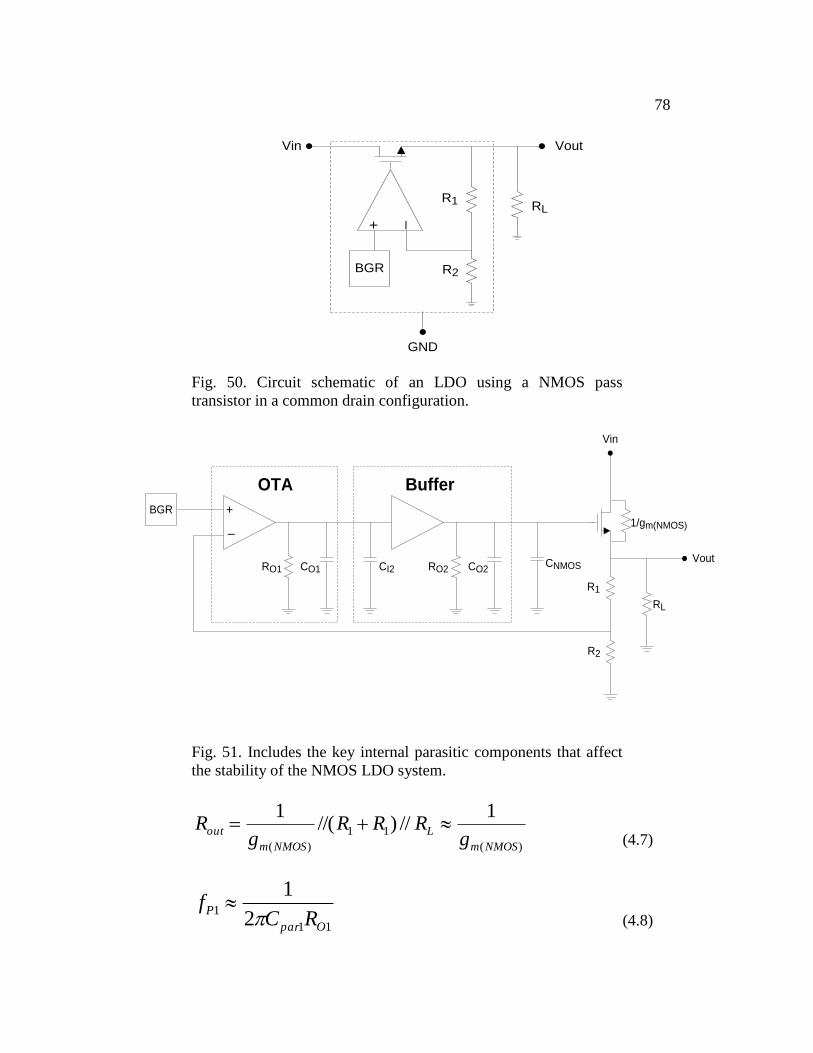
78
Fig. 50. Circuit schematic of an LDO using a NMOS pass
transistor in a common drain configuration.
Vin
+
_
Vout
RL
R1
R2
RO1 CO1 CI2 RO2 CO2CNMOS
OTA Buffer
BGR1/gm(NMOS)
Fig. 51. Includes the key internal parasitic components that affect
the stability of the NMOS LDO system.
)(
11
)(
1//)//(
1
NMOSm
L
NMOSm
outg
RRRg
R (4.7)
11
12
1
Opar
PRC
f
(4.8)
+ _
Vin Vout
GND
BGR
RLR1
R2
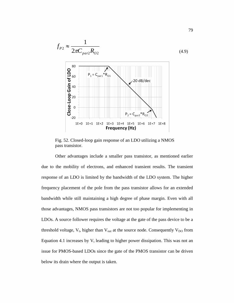
79
22
22
1
Opar
PRC
f
(4.9)
Fig. 52. Closed-loop gain response of an LDO utilizing a NMOS
pass transistor.
Other advantages include a smaller pass transistor, as mentioned earlier
due to the mobility of electrons, and enhanced transient results. The transient
response of an LDO is limited by the bandwidth of the LDO system. The higher
frequency placement of the pole from the pass transistor allows for an extended
bandwidth while still maintaining a high degree of phase margin. Even with all
those advantages, NMOS pass transistors are not too popular for implementing in
LDOs. A source follower requires the voltage at the gate of the pass device to be a
threshold voltage, Vt, higher than Vout at the source node. Consequently VDO from
Equation 4.1 increases by Vt leading to higher power dissipation. This was not an
issue for PMOS-based LDOs since the gate of the PMOS transistor can be driven
below its drain where the output is taken.

80
Charge pumps and servo-based control loops are common tactics used for
removing Vt from VDO. Their presence enables the gate of the NMOS device to be
higher than the input voltage, Vin. While these may be good solutions for system-
on-a-chip applications that provide modest point-of-load currents, usually less
than 50 mA [38], they begin to add significant output noise and take up
substantial die area for applications that require greater than 100 mA load
currents. State-of-the-art technologies though have considerably reduced the area
required for the charge pump leading to more LDOs employing this topology.
Even so, NMOS-based LDOs are still in the minority.
DSATtloadontNMOSDO VVIRVV *)( (4.10)
4.3. N-MESFET LDO OVERVIEW
The key point to pull away from the previous section is the enhancement
mode nature of NMOS devices requires the designer to either deal with a high
dropout voltage, refer to Equation 4.10, or to incorporate a charge pump and
accept all its unwanted side effects. N-MESFETs remove the charge pump
dilemma by virtue of being a depletion mode device that can be almost fully
turned on with a gate-to-source voltage, VGS, equal to 0 V. It is this feature that
allows the MESFET based LDO to be in the inherently stable source follower
configuration of Fig. 53 and have a dropout voltage independent of the threshold
voltage.
The key poles that affect the stability will be the same as
81
Fig. 51 and Equations 4.8 and 4.9. Consequently, it will have a single
pole, closed-loop gain response like Fig. 52. The only difference of note between
the standard NMOS LDO topology and the MESFET LDO in Fig. 53 is it
includes an optional PMOS power down switch which will be explained more in
Section 4.5. This will add some additional parasitic capacitance at the drain of the
MESFET but the contribution will be relatively small since the switch is only a
tenth of the size of the pass transistor. Plus the added parasitic capacitances will
be at the MESFET’s drain node and will be the PMOS’s drain-to-gate and the
drain-to-source capacitances. Both of these are relatively small, thus, the overall
closed-loop response remains virtually unchanged.
Fig. 53. Schematic of the LDO regulator using an N-MESFET pass
transistor.
4.4. SELECTING N-MESFET PASS DEVICE
The N-MESFET LDO that was fabricated and tested was based on the FD-
MESFET shown in Fig. 54. Fig. 54 shows the MESFET’s measured and

82
simulated drain and gate current at a drain-to-source voltage equal to 25 mV. 25
mV was taken as the bias point since it represented the original goal for dropout
voltage performance at a 50 mA load. The device encompasses the basic layout
structure presented in Fig. 27. Its core characteristics are as follows: 150 channels,
Lg = 1.8 μm, LCW = 1 μm, LaS = 0.6 μm (poly), LaD = 1.2 μm (SB), Vt ≈ 0.8V, and
it was doped with the heavy implant (refer to Chapter 3 for more information on
how these characteristics affect the FD-MESFET’s operation). This particular
device was fabricated on a process run that took place in 2007, about a year and a
half before the LDO was fabricated. It was chosen from an assortment of other
MESFETs for four primary reasons: current drive per die area, threshold voltage,
expected RF performance, and die-to-die consistency in performance. The actual
pass device was made with 103,680 channels and is approximately 691x larger.
As mentioned in Chapters 1-3, MESFETs have a natural high breakdown
capability. The breakdown of this MESFET is > 7 V which is about twice the
breakdown of the SOS CMOS on the same process.
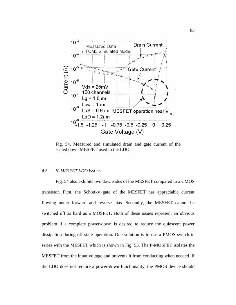
83
Fig. 54. Measured and simulated drain and gate current of the
scaled down MESFET used in the LDO.
4.5. N-MESFET LDO ISSUES
Fig. 54 also exhibits two downsides of the MESFET compared to a CMOS
transistor. First, the Schottky gate of the MESFET has appreciable current
flowing under forward and reverse bias. Secondly, the MESFET cannot be
switched off as hard as a MOSFET. Both of these issues represent an obvious
problem if a complete power-down is desired to reduce the quiescent power
dissipation during off-state operation. One solution is to use a PMOS switch in
series with the MESFET which is shown in Fig. 53. The P-MOSFET isolates the
MESFET from the input voltage and prevents it from conducting when needed. If
the LDO does not require a power-down functionality, the PMOS device should

84
be removed since it will increase the dropout in accordance with Equation 4.11.
However, since the PMOS device is driven hard (VGS = -Vin), the Ron(PMOS) is
small and does not require substantial silicon area to reduce its resistance. In fact,
the PMOS device only accounts for about 10% of the total die area and < 4% of
the total dropout voltage at a load of 75 mA. Fig. 55 shows the complete effect of
the PMOS switch across all loads.
)()(
)()( *)(
PMOSDSATMESNDSAT
loadPMOSonMESNonDO
VV
IRRV
(4.11)
0
50
100
150
200
0 10 20 30 40 50 60 70 80
Load Current (mA)
Total Dropout
Dro
pout V
oltag
e (
mV
)
Dropout: PMOS Power-Down Switch
Fig. 55. Measured total dropout voltage resulting from the PMOS
power-down switch and N-MESFET pass device. Also shown is
the contribution from only the PMOS switch.
For most operating regimes, the Schottky gate of the MESFET will be
reversed biased. This causes the gate current to flow away from the load, out of
the gate, and contribute to the ground current, Ignd. Near the dropout voltage
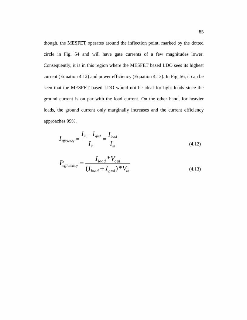
85
though, the MESFET operates around the inflection point, marked by the dotted
circle in Fig. 54 and will have gate currents of a few magnitudes lower.
Consequently, it is in this region where the MESFET based LDO sees its highest
current (Equation 4.12) and power efficiency (Equation 4.13). In Fig. 56, it can be
seen that the MESFET based LDO would not be ideal for light loads since the
ground current is on par with the load current. On the other hand, for heavier
loads, the ground current only marginally increases and the current efficiency
approaches 99%.
in
load
in
gndin
efficiencyI
I
I
III
(4.12)
ingndload
outloadefficiency
VII
VIP
*)(
*
(4.13)
86
86
88
90
92
94
96
98
100
0.5
0.55
0.6
0.65
0.7
0.75
0 10 20 30 40 50 60
Eff
icie
ncy (
%)
Gro
und C
urre
nt, Ig
nd (m
A)
Load Current (mA)
Vin = Vout + VDO
Fig. 56. Measured ground current and current efficiency versus
load current. At higher loads the current efficiency approaches
99%.
Another problematic issue with ground current arises from the steep
negative slope of the reverse bias gate leakage; see Fig. 54. As the input voltage
increases, the VDS across the pass transistor increases making it easier for the
LDO to supply the load current. In order to maintain regulation, the negative
feedback of the LDO loop responds by driving the VGS of the MESFET more
negative. This not only drives the operating point away from the point of
inflection where the gate current is the lowest but further up the gate leakage
curve. Under very light or no load conditions the gate bias point will approach the
MESFET’s pinch-off point which is where the gate and drain currents meet. Due
to this, the threshold voltage plays an important role in the overall ground current
of the LDO since the pinch-off point will be related to it. The threshold voltage

87
also determines how hard the device turns on at VGS = 0 V so there is a tradeoff
that exists.
4.6. MEASUREMENT SETUP & PCB BOARD DESIGN
The PCB test board in Fig. 57 was schematically designed in National
Instrument’s (NI) Multisim program and exported to NI’s Ultiboard for layout.
The board incorporated several test points through the use of 2 x 1 headers to
measure node voltages and currents (the headers are the components labeled with
J in Fig. 57). The headers also enabled the board to only connect components that
were necessary for each particular test. Below is a list of the different
measurements included in this thesis as well as a brief description of how the PCB
was configured to perform the measurements.
1. Ground Current: The input current was measured through J2 and was
compared to the load current measured through J16 (Fig. 56).
2. Dropout Voltage: Vin was swept with a HP 4155B semiconductor
parameter analyzer. The dropout voltage was measured at the point
where Vout dipped to 98% of its nominal output voltage. Through
different combinations of J7-J9 (Fig. 55), the LDO could measure the
dropout voltage at eight different current loads.
3. Transient Line Regulation: A HP 8110A pulse generator was used to
quickly step Vin from a voltage comfortably above dropout to a voltage

88
100-200 mV above that (Fig. 59). Vin and Vout were captured with an
Agilent 54832D oscilloscope and HP 10073A scope probes.
4. Transient Load Regulation: The same HP 8110A was used to quickly
switch the gate of a 2N3904 BJT. When the BJT was turned on, ~10
mA was added to the load through R2. Vin and Vout were also captured
with the Agilent 54832D oscilloscope and HP 10073A scope probes.
5. PSRR: The input ripple (50 mVpp) was created with a HP33120A
waveform generator. The small Vout ripple was then measured with a
SR844 RF lock in amplifier.
Other notes: The PMOS switch could be switched on and off through J12.
J13 allowed an off-chip capacitor to be connected at the output of the bandgap
gap reference to suppress noise. J14 was connected at the drain of the PMOS
switch as a way to measure the dropout contribution from only the PMOS switch
(Fig. 55).

89
Fig. 57. Multisim schematic of the PCB test board.
A die micrograph of the LDO and PCB is shown in Fig. 58a and b
respectively. The area of the layout, omitting the pads, is approximately 2.8 x 1
mm with the MESFET pass transistor contributing ~ 85% of the area. The PCB
was two sided, 2” x 2,” and plated with gold. The bond wires were also gold and
were in the range of about 2 to 3 mm. To minimize the dropout contributed by the
bond wires, about 20 bond wires were each used for Vin and Vout. The resistors
and the noise reducing capacitor soldered to the board were surface mount
components in either 0805 or 0603 packages while the 2N3904 BJT was in a TO-
92 package. The 2N3904 BJT was chosen for its very low input capacitance; ~8
pF. With it, the load contributed by R2 (Fig. 57) could be switched on and off in
about 100 ns. Refer to Appendix A for a table of the 2N3904’s electrical
characteristics. Lastly, an epoxy coating was placed over the die and the bond
wires for the sole purpose of protecting it. It did not aid or alter its operation.
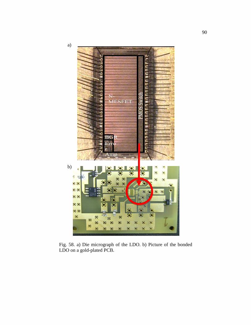
90
Fig. 58. a) Die micrograph of the LDO. b) Picture of the bonded
LDO on a gold-plated PCB.
a)
b)
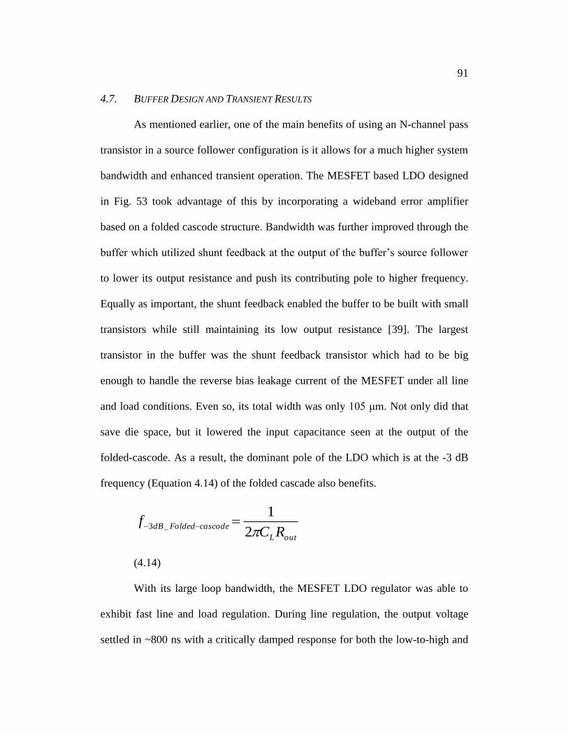
91
4.7. BUFFER DESIGN AND TRANSIENT RESULTS
As mentioned earlier, one of the main benefits of using an N-channel pass
transistor in a source follower configuration is it allows for a much higher system
bandwidth and enhanced transient operation. The MESFET based LDO designed
in Fig. 53 took advantage of this by incorporating a wideband error amplifier
based on a folded cascode structure. Bandwidth was further improved through the
buffer which utilized shunt feedback at the output of the buffer’s source follower
to lower its output resistance and push its contributing pole to higher frequency.
Equally as important, the shunt feedback enabled the buffer to be built with small
transistors while still maintaining its low output resistance [39]. The largest
transistor in the buffer was the shunt feedback transistor which had to be big
enough to handle the reverse bias leakage current of the MESFET under all line
and load conditions. Even so, its total width was only 105 μm. Not only did that
save die space, but it lowered the input capacitance seen at the output of the
folded-cascode. As a result, the dominant pole of the LDO which is at the -3 dB
frequency (Equation 4.14) of the folded cascade also benefits.
outL
cascodeFoldeddBRC
f2
1_3
(4.14)
With its large loop bandwidth, the MESFET LDO regulator was able to
exhibit fast line and load regulation. During line regulation, the output voltage
settled in ~800 ns with a critically damped response for both the low-to-high and
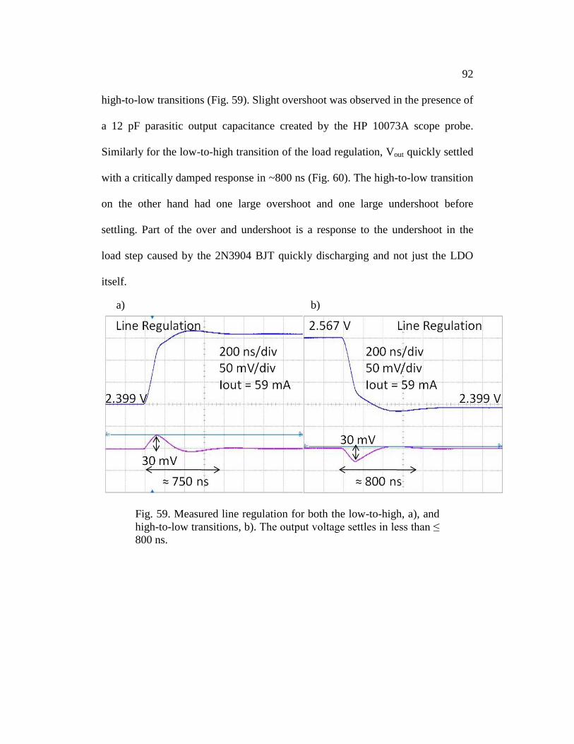
92
high-to-low transitions (Fig. 59). Slight overshoot was observed in the presence of
a 12 pF parasitic output capacitance created by the HP 10073A scope probe.
Similarly for the low-to-high transition of the load regulation, Vout quickly settled
with a critically damped response in ~800 ns (Fig. 60). The high-to-low transition
on the other hand had one large overshoot and one large undershoot before
settling. Part of the over and undershoot is a response to the undershoot in the
load step caused by the 2N3904 BJT quickly discharging and not just the LDO
itself.
Fig. 59. Measured line regulation for both the low-to-high, a), and
high-to-low transitions, b). The output voltage settles in less than ≤
800 ns.
a) b)

93
Fig. 60. Measured load regulation for both the low-to-high, a), and
high-to-low transitions, b). The output voltage settles in less than ≤
1 µs.
4.8. PSRR RESULTS
The PSRR is a figure of merit of how well a LDO can suppress
disturbances at the input (Equation 4.15) and is a function of the error amplifier,
pass transistor, and feedback resistors. For noise sensitive RF applications, like
cell phones, it is absolutely necessary to have a high PSRR. The roll off in PSRR
was around 10 kHz in this case (Fig. 61) and was set by the dominant pole found
in Equation 4.8. The rest of the degradation in PSRR with respect to frequency
coincides with the loop bandwidth of the LDO. There are number of ways to
improve the PSRR including improving the gain of the error amplifier and/or
adding a cascode structure between the pass transistor and supply [36, 40]. For
this LDO, the PSRR was about 45 dB for frequencies less than 10 kHz at loads of
10.8 mA and 34 mA (Fig. 61).
a) b)

94
rippleout
ripplein
V
VPSRR
,
,
10log20 (4.15)
0
10
20
30
40
50
60
70
102
103
104
105
PS
RR
(d
B)
Frequency (Hz)
Iout = 34 mA
Iout = 10.8 mA
Vin = 2.35 V + 0.05 Vpp
Fig. 61. PSRR for loads of 10.8 and 34 mA.
4.9. IMPROVING FD-MESFET LDOS
One way to improve the performance of the LDO is to design the
MESFET with the same characteristics listed in Section 4.4 but with the structure
in Fig. 36. As shown in Fig. 37, both the current drive and gate current improved
in their respective matter. This type of device was not chosen for this particular
LDO since the device was not fabricated on the 2007 process run. Without having
the MESFET to characterize, there was no way to accurately model the device.
There were other similar MESFETs which could have been used to approximate
its operation, but if the estimated model was off, particularly with respect to the

95
RF parameters, it ran the risk that the final LDO would not be stable without an
external load capacitor. There was also the risk that the device would not work.
That risk is relatively small though since the majority of the MESFETs fabricated
with Peregrine have worked in some capacity including those that are similar to
the one being proposed. Nevertheless, the most conservative route was chosen for
the first design run.
Another option for improving the LDO would be to use a more state-of-
the-art FD-CMOS process or having a 0.25 μm FD technology that is more
aggressively scaled with respect to the backend metal layers. In this particular
process the backend metals were similar to that of 0.6 μm process. Even slight
reductions in layout rules will lead to sizable savings in die space due to the sheer
number of channels. For example, if the layout was done on Peregrine’s new 0.25
μm process with everything in the layout exactly the same expect for the
MESFET, the LDO die area would be 511 x 195.7 µm smaller. That is equates to
about a 35% reduction. The new process would also shrink the gate length from
1.8 µm to 1.15 µm. If previous MESFET performance with respect to gate length
holds true, a 25-35% increase in current drive can be also be expected. Likewise
there should be a similar reduction in gate current. Table 5 summarizes the layout
rules that affect the MESFET. The GC process was the process used for this LDO
and the Px process is Peregrine’s newer process.

96
Table 5: Improvements in Peregrine’s Newer Process
Parameter GC Process Px Process
Contact 0.6 x 0.6 µm 0.4 x 0.4 µm
Contact to Contact 0.8 µm 0.35 µm
Contact to Poly 0.6 µm 0.4 µm
Contact to SB 0.6 µm 0.6 µm
Metal1 to Metal1 0.8 µm 0.4 µm
4.10. CONCLUSIONS
The final results of the LDO are summarized in Table 6. The LDO
featured fast responses, < 1 µs, to changes in line and load and was stable under
all conditions without an external capacitor. It proved MESFETs can work
effectively as a pass transistor and be easily integrated with a complex analog
circuit. While the MESFET does require a large die size to achieve its dropout
voltage and current rating, it is important to consider that it is performing on a
FD-CMOS process and the gate length was limited to 1.8 µm by the layout rules.
Significant improvements can be achieved though on FD-CMOS processes with a
different MESFET layout structure such as Fig. 36 and/or a slightly more
advantageous process with smaller BEOL design rules such as the Px process
from Peregrine.

97
Table 6: LDO Performance Summary
Process 0.25µm SOS CMOS
Vin 2-3V
Vout 2.0V
CLoad N/A
Peak PSRR (Vin = 2.36V + 0.05Vpp) 48dB
VDO (Iout = 75mA) 180mV
Current Efficiency (Vin = Vout + VDO & Iout > 20mA) 97%
Line Regulation (L-H & Iout = 59mA) ΔV = 30mV, Δt = 750ns
Line Regulation (H-L & Iout = 59mA) ΔV = 30 mV, Δt = 800ns
Load Regulation (L-H & Vin = 2.4V) ΔV = 123mV, Δt = 800ns
Load Regulation (H-L & Vin = 2.4V) ΔV1 = 97mV, ΔV2 = 37mV, Δt = 1µs

98
CHAPTER 5
PD SOI MESFET LDOs
The FD-MESFET LDO from Chapter 4 presented a unique yet simple
solution for an n-channel LDO. Due to a few key design rules though which
adversely affected the layout size of the MESFET and consequently its current
drive, that LDO was not a practical solution. As will be shown in this chapter,
better and possibly state-of-the-art performance can be obtained by switching to a
PD-CMOS process and using a PD-MESFET as the pass transistor. With fewer
layout rules restricting their design, the gate length and device structure can be
made much more compact. This is evident with the PD-MESFETs fabricated on
the Honeywell 0.15 µm PD-SOI CMOS process in Chapter 2. While gate lengths
on that process were conceivably able to scale down to 0.15 µm, good depletion
mode behavior combined with good output resistance characteristics was not seen
until Lg ~0.3 µm. Still using that Lg = 0.3 µm device converts to a current drive
per die area that is more than 20x greater than the one chosen in Chapter 4 and a
gate leakage current that is over 100x smaller (Fig. 62 and Table 7). From a
design perspective, the reduced leakage current lessens the constraints on the
buffer and allows for a simpler architecture to be used.
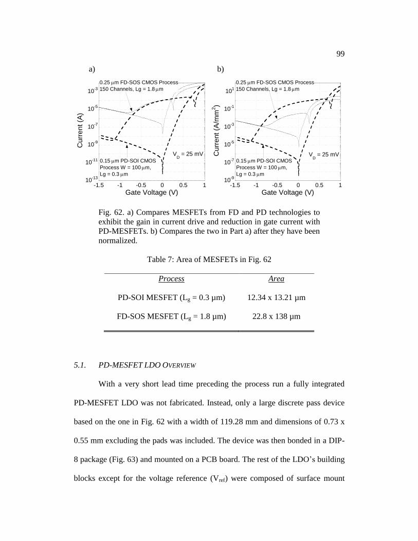
99
10-13
10-11
10-9
10-7
10-5
10-3
-1.5 -1 -0.5 0 0.5 1
Cu
rre
nt
(A)
Gate Voltage (V)
VD = 25 mV
0.15 m PD-SOI CMOS
Process W = 100 m,
Lg = 0.3 m
0.25 m FD-SOS CMOS Process
150 Channels, Lg = 1.8 m
10-9
10-7
10-5
10-3
10-1
101
-1.5 -1 -0.5 0 0.5 1
Cu
rre
nt
(A/m
m2)
Gate Voltage (V)
VD = 25 mV
0.15 m PD-SOI CMOS
Process W = 100 m,
Lg = 0.3 m
0.25 m FD-SOS CMOS Process
150 Channels, Lg = 1.8 m
Fig. 62. a) Compares MESFETs from FD and PD technologies to
exhibit the gain in current drive and reduction in gate current with
PD-MESFETs. b) Compares the two in Part a) after they have been
normalized.
Table 7: Area of MESFETs in Fig. 62
Process Area
PD-SOI MESFET (Lg = 0.3 µm) 12.34 x 13.21 µm
FD-SOS MESFET (Lg = 1.8 µm) 22.8 x 138 µm
5.1. PD-MESFET LDO OVERVIEW
With a very short lead time preceding the process run a fully integrated
PD-MESFET LDO was not fabricated. Instead, only a large discrete pass device
based on the one in Fig. 62 with a width of 119.28 mm and dimensions of 0.73 x
0.55 mm excluding the pads was included. The device was then bonded in a DIP-
8 package (Fig. 63) and mounted on a PCB board. The rest of the LDO’s building
blocks except for the voltage reference (Vref) were composed of surface mount
a) b)

100
components. To show the versatility of the PD-MESFET LDO, two different
flavors of error amplifiers were used in measurements. One exhibited very low
quiescent current, Iq, while the other had a moderate Iq, but a much larger
bandwidth (refer to Appendix A for the datasheets of both devices). All the
voltages including Vref was supplied and monitored by an HP4155B parameter
analyzer. Lastly, R1 and R2 were chosen so Vout was 1.8 V and DC measurements
were limited to 100mA due the compliance of the HP4155B.
Fig. 63. Simple circuit schematic of the board level LDO design
with a picture of the bonded out die. The device excluding pads is
0.73 x 0.55 mm while the cavity of the DIP-8 package is 7.37 x
4.32 mm.
The design of the PCB board (Fig. 64) was very similar to the one in
Chapter 4. Once again, a 2N3904 BJT was included to conduct load transient
measurements and a series of 2 x 1 headers were added to enable the board to
connect only the necessary components for each particular test. The only major
difference was electing to use a DIP-8 package instead of bonding the bare die
directly to the board. This dramatically increased the flexibility for testing and
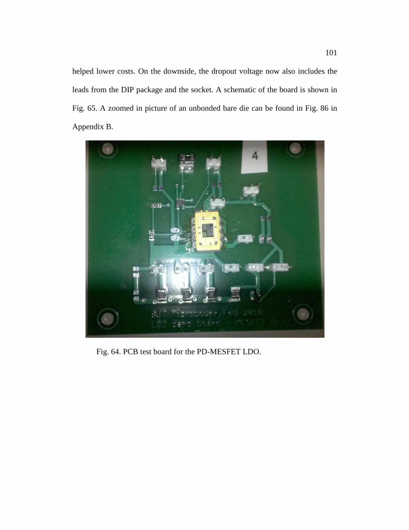
101
helped lower costs. On the downside, the dropout voltage now also includes the
leads from the DIP package and the socket. A schematic of the board is shown in
Fig. 65. A zoomed in picture of an unbonded bare die can be found in Fig. 86 in
Appendix B.
Fig. 64. PCB test board for the PD-MESFET LDO.
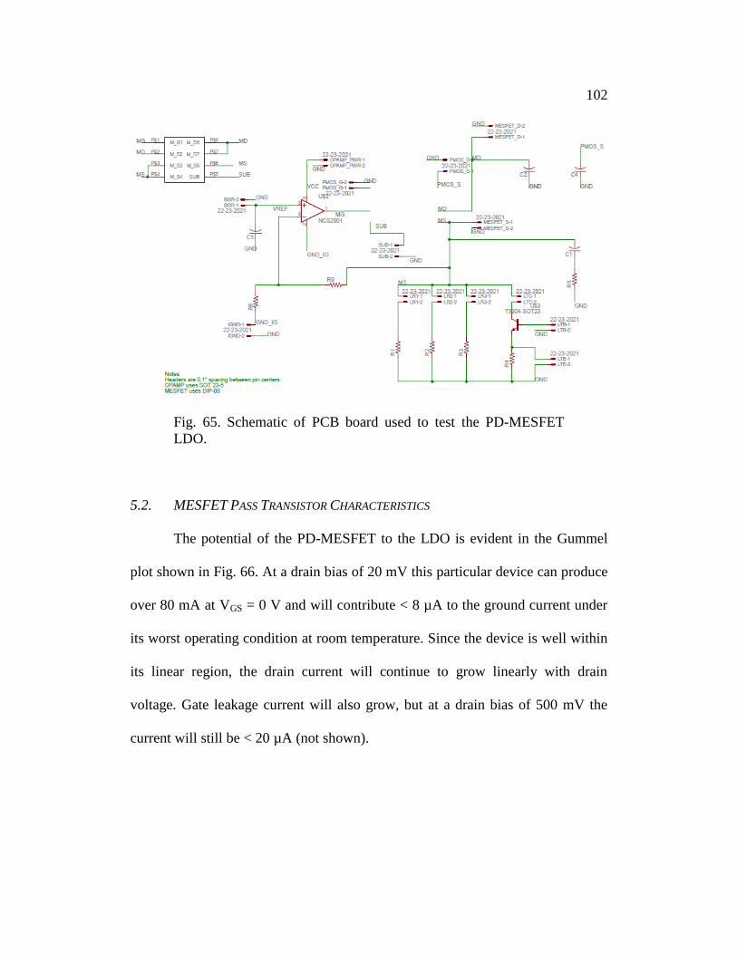
102
Fig. 65. Schematic of PCB board used to test the PD-MESFET
LDO.
5.2. MESFET PASS TRANSISTOR CHARACTERISTICS
The potential of the PD-MESFET to the LDO is evident in the Gummel
plot shown in Fig. 66. At a drain bias of 20 mV this particular device can produce
over 80 mA at VGS = 0 V and will contribute < 8 µA to the ground current under
its worst operating condition at room temperature. Since the device is well within
its linear region, the drain current will continue to grow linearly with drain
voltage. Gate leakage current will also grow, but at a drain bias of 500 mV the
current will still be < 20 µA (not shown).

103
10-9
10-8
10-7
10-6
10-5
10-4
10-3
10-2
10-1
-2 -1.5 -1 -0.5 0 0.5 1
Curr
ent (A
)
Gate Voltage (V)
VD = 20 mV
Fig. 66. Gummel plot of bonded out PD-MESFET pass transistor.
With the FOC plot hitting the HP4155B’s compliance fairly quickly (Fig.
67a), the output characteristics of the pass transistor cannot be seen, however, the
on resistance, Ron, can still be extracted. At VGS = 0 V, Ron is ~240 mΩ which
corresponds to ~96 mΩ/mm2. In reality Ron is less than 240 mΩ since that figure
includes the resistance of the DIP-8 package leads and the long bondwires. These
parasitics are unavoidable for all LDOs, but with an appropriately sized package,
the bondwires could be made a fraction of their current size.
Fig. 67b shows the FOC out to 5 V for a MESFET exactly 1/28 the size
(W = 4.26 mm) of the pass transistor. A soft breakdown begins to appear at ~4V
which is more than twice the maximum safe operating voltage of the SOI CMOS
(1.95V). Neglecting the parasitic resistances from the long metal lines of the pass
transistor and the corresponding voltage drops, it can be expected that the pass

104
transistor will have a drain current roughly 28x larger than Fig. 67b. The gate
current should also scale proportionately.
0
20
40
60
80
100
120
0 10 20 30 40 50 60 70Drain Voltage (mV)
Curr
ent (m
A)
0V to -0.5V in 100mV steps
0
20
40
60
80
100
120
0 1 2 3 4 5
Dra
in C
urr
en
t (m
A)
Drain Voltage (V)
0V to -1V in 100mV steps
Fig. 67. a) FOC for MESFET pass transistor. b) FOC of MESFET
that is 1/28 the size of the pass transistor.
5.3. PD-MESFET LDO RESULTS
Unlike the FD-MOSFET LDO in Chapter 4 (Fig. 56), the worst case
ground current for this LDO occurs at no load. This will generally be the case for
FD or PD-MESFET LDOs. In each type of MESFET the slope of the Schottky
gate leakage curve increases with decreasing VGS. As the load becomes easier for
the MESFET to the drive, the feedback of the LDO will begin to shut the
MESFET off and push the bias point of the MESFET to higher position on the
gate leakage curve. This is analogous to the effect that increasing input voltage
has on the LDO (explained in Section 4.5).
b) a)
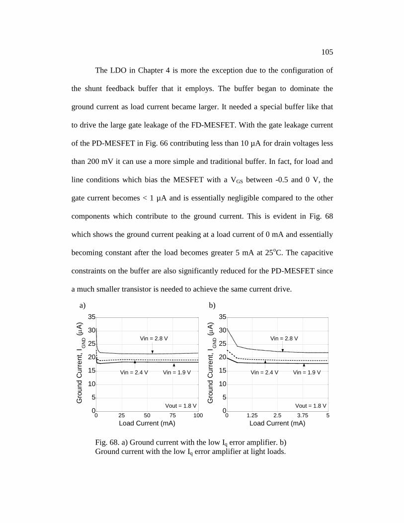
105
The LDO in Chapter 4 is more the exception due to the configuration of
the shunt feedback buffer that it employs. The buffer began to dominate the
ground current as load current became larger. It needed a special buffer like that
to drive the large gate leakage of the FD-MESFET. With the gate leakage current
of the PD-MESFET in Fig. 66 contributing less than 10 µA for drain voltages less
than 200 mV it can use a more simple and traditional buffer. In fact, for load and
line conditions which bias the MESFET with a VGS between -0.5 and 0 V, the
gate current becomes < 1 µA and is essentially negligible compared to the other
components which contribute to the ground current. This is evident in Fig. 68
which shows the ground current peaking at a load current of 0 mA and essentially
becoming constant after the load becomes greater 5 mA at 25oC. The capacitive
constraints on the buffer are also significantly reduced for the PD-MESFET since
a much smaller transistor is needed to achieve the same current drive.
0
5
10
15
20
25
30
35
0 25 50 75 100
Load Current (mA)
Gro
un
d C
urr
ent,
IG
ND (
A)
Vin = 2.8 V
Vout = 1.8 V
Vin = 1.9 VVin = 2.4 V
0
5
10
15
20
25
30
35
0 1.25 2.5 3.75 5
Load Current (mA)
Gro
un
d C
urr
ent,
IG
ND (
A)
Vin = 2.8 V
Vout = 1.8 V
Vin = 1.9 VVin = 2.4 V
Fig. 68. a) Ground current with the low Iq error amplifier. b)
Ground current with the low Iq error amplifier at light loads.
a) b)

106
As was the case for the LDO in Chapter 4, this LDO shows fast and stable
recovery for both the line and load transient response (Fig. 69-Fig. 72) without an
output capacitor. The line and load for the low Iq error amplifier recovers in < 15
µs while the moderate Iq error amplifier’s expanded gain bandwidth allows it to
recover in 2 µs or less. The larger transient spikes in the low Iq error amplifier
design can be attributed to the error amplifier’s slower slew rate. This can be
expected given its much lower Iq. The slew rate issue becomes very evident in
capacitor less LDO regulators particularly at fast transients [40].
Fig. 69. Transient line regulation with the low Iq error amplifier.
Iout = 50 mA, tr = tf = 200 ns and T = 50 µs.
1.5
1.6
1.7
1.8
1.9
2
2.1
Outp
ut V
oltage
(V
)
1.5
2
2.5
3
3.5
0 5 10 15
Inp
ut
Vo
lta
ge
(V
)
Time (s)25 30 35 40
Time (s)

107
Fig. 70. Transient line regulation with the moderate Iq error
amplifier. Iout = 50 mA, tr = tf = 200 ns and T = 50 µs.
Fig. 71. Transient load regulation with the low Iq error amplifier. Vin = 2.4 V, tr =
tf = 500 ns and T = 50 µs.
1.2
1.4
1.6
1.8
2
2.2
2.4
Outp
ut V
oltage
(V
)
-50
0
50
100
150
200
0 5 10 15 20
Lo
ad C
urr
ent
(mA
)
Time (s)25 30 35 40 45
Time (s)
1.7
1.75
1.8
1.85
1.9
Outp
ut V
oltage
(V
)
2
2.2
2.4
2.6
2.8
3
2 4 6 8 10
Inpu
t V
oltage
(V
)
Time (s)28 30 32 34 36
Time (s)

108
Fig. 72. Transient load regulation with the moderate Iq error
amplifier. Vin = 2.4 V, tr = tf = 500 ns and T = 50 µs.
5.4. PD-MESFET LDO RESULTS ACROSS TEMPERATURE
The PD-MESFET LDO was measured from -50 to +150oC and showed
excellent characteristics across the entire range. A temperature controlled oven
provided the measurements between 25 and 150oC while a probe station with a
cooled stage was used for the -50oC measurement. As shown in Fig. 73, Fig. 74,
and Fig. 87-Fig. 89 (refer to Appendix C) the output voltage changed only
minimally under different line, load, and temperature conditions. It should be
noted though, these numbers are extremely overly optimistic since the voltage
reference was a precision voltage source that was maintained at room
temperature. If this were an integrated LDO with a finely designed voltage
1.5
1.6
1.7
1.8
1.9
2
2.1
2.2
Outp
ut
Vo
ltag
e (
V)
-50
0
50
100
150
200
4 5 6 7 8 9
Outp
ut V
oltage
(V
)
Time (s)
29 30 31 32 33 34
Time (s)
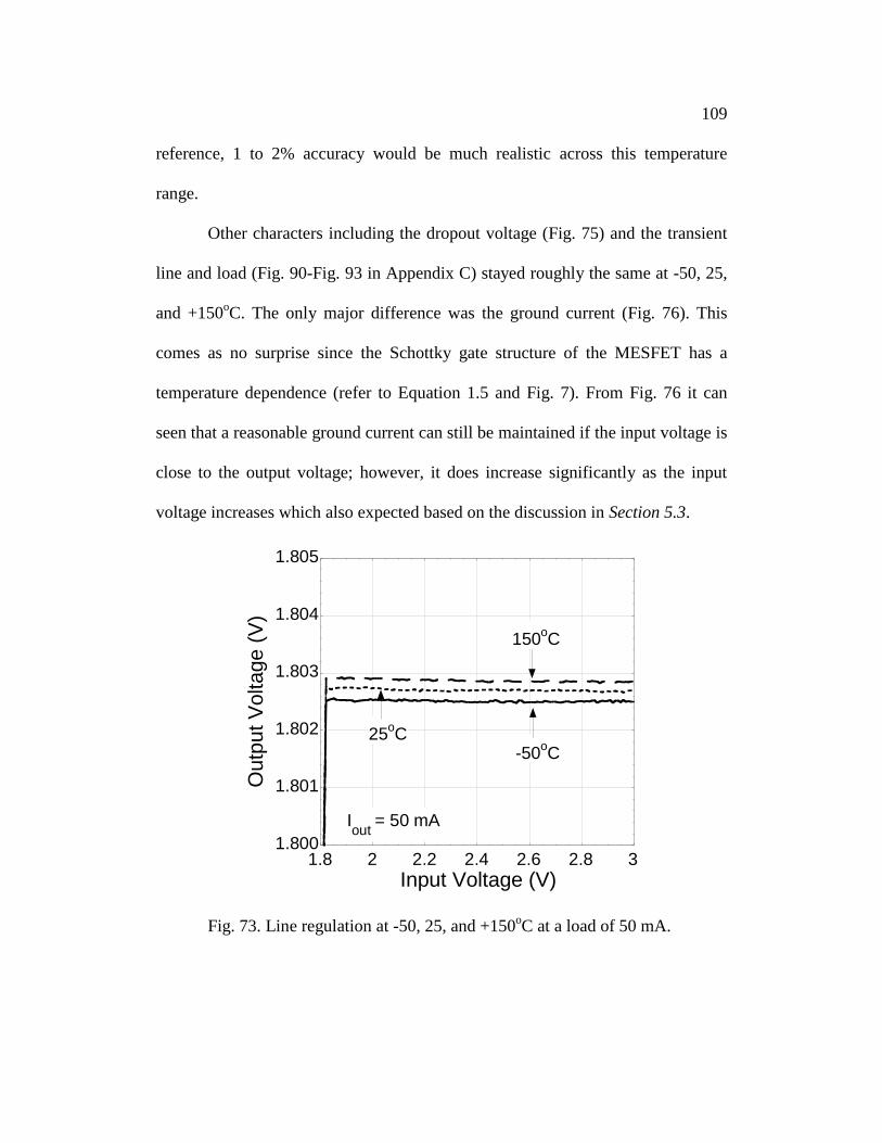
109
reference, 1 to 2% accuracy would be much realistic across this temperature
range.
Other characters including the dropout voltage (Fig. 75) and the transient
line and load (Fig. 90-Fig. 93 in Appendix C) stayed roughly the same at -50, 25,
and +150oC. The only major difference was the ground current (Fig. 76). This
comes as no surprise since the Schottky gate structure of the MESFET has a
temperature dependence (refer to Equation 1.5 and Fig. 7). From Fig. 76 it can
seen that a reasonable ground current can still be maintained if the input voltage is
close to the output voltage; however, it does increase significantly as the input
voltage increases which also expected based on the discussion in Section 5.3.
1.800
1.801
1.802
1.803
1.804
1.805
1.8 2 2.2 2.4 2.6 2.8 3
Outp
ut V
oltage
(V
)
Input Voltage (V)
150oC
Iout
= 50 mA
-50oC
25oC
Fig. 73. Line regulation at -50, 25, and +150oC at a load of 50 mA.

110
1.800
1.801
1.802
1.803
1.804
1.805
0 25 50 75 100
Outp
ut
Vo
ltage
(V
)
Output Current (mA)
150oC
25oC
-50oC
Vin
= 2.4 V
Fig. 74. Load regulation at -50, 25, and +150oC at a Vin = 2.4 V.
0
10
20
30
40
0 50 100 150
Dro
pou
t V
olta
ge (
mV
)
Output Current (mA)
150oC
25oC
-50oC
Fig. 75. The dropout voltage was measured up to 100 mA for -50,
25, and +150oC and extrapolated from 100 to 150 mA.

111
0
25
50
75
100
125
150
0 25 50 75 100
Iout
(mA)
Gro
un
d C
urr
en
t, I
GN
D (
A)
Vin = 2.8 V
Vin = 1.9 V
Vin = 2.4 V
85oC
0
25
50
75
100
125
150
0 1.25 2.5 3.75 5
Iout
(mA)
Gro
un
d C
urr
en
t, I
GN
D (
A)
Vin = 2.8 V
Vin = 1.9 V
Vin = 2.4 V
85oC
Fig. 76. a) Ground current at 85oC with the low Iq error amplifier.
b) Ground current at 85oC with the low Iq error amplifier at light
loads.
5.4. LOW VOLTAGE OPPORTUNITIES AND BODY BIAS EFFECTS
With the goal of lowering the overall power consumption of power
management systems, industry has been pushing for LDOs with lower dropout
and output voltages. For PMOS LDOs this brings up a challenge. Typically their
dropout voltage becomes noticeably worse as the output voltage scales below 1.5
V [41-42]. That is a result of the error amplifier running out of headroom to drive
the gate of the PMOS, which in turn causes an increase in the on resistance and
consequently a rise in the dropout voltage. Thus this counteracts some of the
benefits of moving down to lower voltages.
For a PD N-MESFET pass device, the performance should improve since
lowering the output voltage will decrease the body effect on the transistor. This is
evident in Fig. 77 which compares a MESFET pass device under zero body effect
a) b)

112
(VBS = 0 V) and at VBS = -1.8 V. The latter is the equivalent to what the MESFET
sees when the LDO is at an output of 1.8 V. Without the body effect it is clear the
device turns on earlier and has a higher drive current at VGS = 0 V. Using this
idea, it is possible to improve the performance of the dropout by tying the source
(Vout) to the substrate. From Fig. 78 it can be seen that this leads to roughly a 10%
improvement. The amount of improvement will be dependent on the MESFET’s
sensitivity to body effect which is related to the thickness of the insulating layer.
On the Honeywell 150 nm process, the oxide was about 1 µm. It should be noted
though that biasing the substrate might affect the operation of the CMOS. Also
the dropout results are slightly different in Fig. 78 and Fig. 75 since a different
bonded MESFET pass device was used. Lastly, while this might be an effective
method for PD-MESFETs, FD-MESFETs cannot be improved in this manner
since the silicon channel below the gate is fully depleted under all biasing
conditions and is unaffected by body effect.
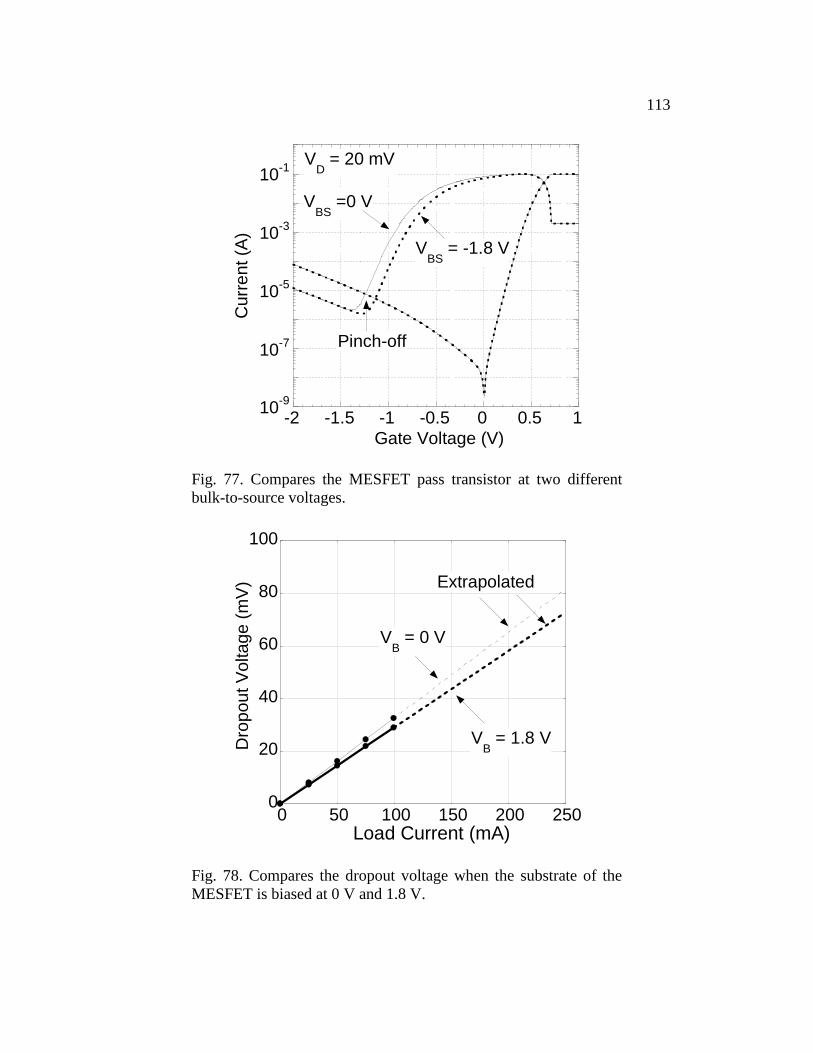
113
10-9
10-7
10-5
10-3
10-1
-2 -1.5 -1 -0.5 0 0.5 1
Curr
en
t (A
)
Gate Voltage (V)
VD = 20 mV
VBS
= -1.8 V
VBS
=0 V
Pinch-off
Fig. 77. Compares the MESFET pass transistor at two different
bulk-to-source voltages.
0
20
40
60
80
100
0 50 100 150 200 250
Dro
po
ut V
olta
ge
(m
V)
Load Current (mA)
Extrapolated
VB = 0 V
VB = 1.8 V
Fig. 78. Compares the dropout voltage when the substrate of the
MESFET is biased at 0 V and 1.8 V.

114
Although the drive current improves as the output voltage scales there is a
practical limitation on how low it can it go. That value is determined by the
MESFET’s pinch-off voltage. In order to limit the amount of conducting current
during no load or very light load conditions, enough headroom needs to be
allocated so that a large enough negative VGS can be generated across the
MESFET’s gate-to-source junction to pinch it off. Based on that, the lowest
output voltage for this particular MESFET would be ~1.25 V. However if a lower
output voltage is needed, a MESFET with a slightly larger gate length and one
which is less affected by short channel effects can be used. In Fig. 16 it can be
seen that MESFETs on the same process had threshold voltage as low as -0.4 V.
The other option would be to reduce the thickness of the thin silicon channel (Fig.
26). Both these options though would depress the pass transistor’s current drive
per die area and lead to a higher dropout voltage. Nevertheless, either option
might be more attractive for very low voltage applications than the traditional
PMOS LDO topology.
5.5. RADIATION EFFECTS ON MESFET LDO
The MESFET has a natural tolerance to radiation due to its Schottky gate
structure which is less susceptible to radiation damage than the MOS gate of a
CMOS transistor. Unfortunately, while the gate can avoid significant damage, the
spacers used for the access regions and the buried oxide layer will be affected in
the form of induced positive trapped charge. This as result will cause an influx of

115
electrons to travel away from the heavily doped source and drain regions and into
the channel region to balance out the positive trapped charge. Consequently, the
device sees a negative threshold shift since a more negative gate bias is now
needed to fully deplete the channel and pinch it off [43]. This is confirmed in Fig.
79 which shows the Gummel plot of the MESFET before and after radiation. An
unintended yet positive consequence of this is the dropout voltage (Fig. 94 in
Appendix D) will drop slightly with the device being able to be turned on harder
at VGS = 0 V. Predictably the increased leakage can be attributed to the extra
electrons in the silicon channel after radiation.
10-9
10-8
10-7
10-6
10-5
10-4
10-3
10-2
10-1
-2 -1.5 -1 -0.5 0 0.5 1
Cu
rre
nt
(A)
Gate Voltage (V)
VD = 15 mV
After 1 Mrad(Si)
Before Radiation
Fig. 79. Compares the Gummel plot of MESFET pass device after
an exposure dose of 1 Mrad(Si).
With the expectation of the ground current incrementally rising with
exposure dose, the operation of the PD-MESFET LDO was fairly constant
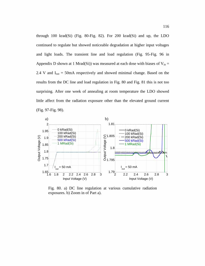
116
through 100 krad(Si) (Fig. 80-Fig. 82). For 200 krad(Si) and up, the LDO
continued to regulate but showed noticeable degradation at higher input voltages
and light loads. The transient line and load regulation (Fig. 95-Fig. 96 in
Appendix D shown at 1 Mrad(Si)) was measured at each dose with biases of Vin =
2.4 V and Iout = 50mA respectively and showed minimal change. Based on the
results from the DC line and load regulation in Fig. 80 and Fig. 81 this is not too
surprising. After one week of annealing at room temperature the LDO showed
little affect from the radiation exposure other than the elevated ground current
(Fig. 97-Fig. 98).
1.65
1.7
1.75
1.8
1.85
1.9
1.95
2
1.6 1.8 2 2.2 2.4 2.6 2.8 3
0 kRad(Si)100 kRad(Si)200 kRad(Si)500 kRad(Si)1 MRad(Si)
Ou
tpu
t V
olta
ge
(V
)
Input Voltage (V)
Iout
= 50 mA
1.79
1.795
1.8
1.805
1.81
2 2.2 2.4 2.6 2.8 3
0 kRad(Si)100 kRad(Si)200 kRad(Si)500 kRad(Si)1 MRad(Si)
Ou
tput
Voltage
(V
)
Input Voltage (V)
Iout
= 50 mA
Fig. 80. a) DC line regulation at various cumulative radiation
exposures. b) Zoom in of Part a).
a) b)

117
1.78
1.8
1.82
1.84
1.86
1.88
0 20 40 60 80 100
0 krad100 krad200 krad500 krad1 Mrad
Ou
tpu
t V
oltag
e (
V)
Load Current (mA)
Vin
= 2.4 V1.79
1.795
1.8
1.805
1.81
0 20 40 60 80 100
0 krad100 krad200 krad500 krad1 Mrad
Ou
tpu
t V
oltag
e (
V)
Load Current (mA)
Vin
= 2.4 V
Fig. 81. a) DC load regulation at various cumulative radiation
exposures. b) Zoom in of Part a).
1.795
1.796
1.797
1.798
1.799
1.800
1 10 100 1000
Ou
tpu
t V
oltag
e (
V)
Radiation Dose (krad)
~~
Vin = 2.4V I
Load = 50 mA
0
Fig. 82. The output voltage of the PD-MESFET LDO at
cumulative radiation doses of 10, 20, 50, 100, 200, 500, and 1000
krad(Si).
a) b)
118
For background purposes a MDS Nordion Gammacell 220 Co60
source
was used to conduct the radiation tests. Tests took place over a two day period
and the dose rate was approximately 0.9 krad(Si/minute). Measurements for DC
line and load regulation, transient line and load regulation, and noise were taken
after cumulative doses of 10, 20, 50, 100, 200, 500, and 1000 krad(Si). Each set of
tests lasted roughly one hour. Upon completion, the MESFET was immediately
put back in the Co60
source to mitigate the effects of room temperature annealing.
Since the LDO was a board level design filled with non-radiation hardened
surface mount components, only the MESFET was exposed. The DIP-8 package
was left without a protective lid or epoxy coating as to not block or absorb the
radiation dose and each pin was grounded during exposure. It should be noted that
the radiation results for this particular MESFET should be further enhanced since
the 150 nm SOI Honeywell process is a radiation hard process. Radiation tests
were also performed on the FD-MESFET LDO from Chapter 4 but due to a
confidentiality agreement with Peregrine Semiconductor those results cannot be
made public. It can be said though that the LDO was still regulating after 1
Mrad(Si). For more radiation results on ASU MESFETs please refer to [43-44].
5.6. CONCLUSION
With these promising preliminary results, the next phase for the PD-
MESFET is to complete a fully integrated design similar to the one in Chapter 4
on the Honeywell 150nm SOI CMOS process. Ideally the performance will

119
improve with respect to the transient responses and ground current since the error
amplifier can be optimally designed to meet the needs of the MESFET LDO.
Moreover with its ultra-low dropout voltage and capacitor free operation, this
LDO appears to be a good fit for high current system-on-chip designs where the
LDO consumes considerable die space and applications where very low dropout
is needed to preserve battery lifetime. Additionally the LDO shows excellent
promise for extreme environment electronics.
120
CHAPTER 6
CONCLUSION
As it was shown in the first four chapters, MESFETs can be integrated on
commercial SOI or SOS CMOS processes without altering the fabrication flow or
adding additional process steps. Thus, they are available to these processes free of
cost. As evident by the LDO examples in Chapter 4 and 5, their unique
characteristics can make them a very effective complement to CMOS
technologies to increase performance and/or lower costs for certain analog
circuits. The LDO benefited from the MESFET’s depletion mode operation as it
allowed it to implement an n-channel pass transistor without allocating precious
die space for a charge pump. Meanwhile with the MESFET’s seamless ability to
integrate with CMOS it allowed for the rest of the building blocks to be designed
with the low power CMOS.
6.1. OPTIMIZING MESFET PASS TRANSISTOR
Moving forward, a key to widening the appeal of the N-MESFET LDO
will be to reduce the gate leakage current. While it was not mentioned in Chapter
2, one of the small improvements made on the 150 nm Honeywell process was
leaving the active silicon under the extended gate region and the edges of the
MESFET for the structure in Fig. 13 at the intrinsic doping level to limit leakage
paths. The reduction in gate current is evident in Fig. 15a and b particularly for
the two Lg = 400 nm devices.

121
Another key will be minimizing parasitics to lower the dropout voltage.
This is particularly important for high current applications where the voltage
drops from the parasitics can dominate the dropout of the MESFET pass
transistor. One mistake that was made for the MESFET pass transistor in Chapter
5 was using only a single via per finger on the drain end to bring the current up to
the higher metal layers (refer to Appendix E for 3-D pictures of the PD-MESFET
layout). Putting multiple vias down the entire finger would have expanded the
drain metal line slightly, but it mostly likely would have been offset by the lower
resistance of the finger. Moreover having additional vias should improve the
reliability of the device since all the current for each finger as it is now flows
through a single via stack.
Finding the optimal finger length and metal bus lines will also be
important in reducing parasitics. For this layout, fingers of 10 µm were used since
that was the finger size of the devices in Chapter 2. Once again, that was left
unchanged to minimize risk. The drain bus line was then run over the device and a
source line of about equal size was run below the device. This more than likely is
not an efficient use of die space. Probably a better solution is to increase the
finger lengths somewhere between 25 and 100 µm and stack the first 2 or 3 metals
layers with minimally spaced vias on each of the source and drain fingers. Then
with the area above the MESFET, source and drain bus lines can be routed with
the top 3 or 4 metal layers. With this method, almost all of the die would be
allocated to the pass device instead of about half of it. To optimally design the

122
MESFET though, a model of the interconnects would eventually need to be
developed. Depending on the current rating of the LDO, the optimal routing
scheme may differ especially at high currents where the pass transistor can
become very large.
6.2. FUTURE LDO OPPORTUNITIES
Assuming a Phase 2 project is approved by NASA, two fully integrated
LDOs based on the MESFET in Chapter 5 will be designed for current ratings of
100 mA and 1 A. While these designs will hopefully have results that will rival
start-of-art LDOs, the potential end customers will likely be limited to NASA and
other government agencies or suppliers who are willing to spend a premium for
Honeywell’s radiation hardened process. To expand the N-MESFET LDO
concept to commercial consumers, plans are on order for a design on IBM’s 180
nm SOI CMOS process. Since this process has not yet been used for the ASU
MESFETs it is likely that an array of marginally sized MESFETs with varying
access and gate lengths will be laid out on the first design run to figure out the
optimal structure. With the lithography rules being more stringent towards the
silicide block layer, devices might include access regions created by the
polysilicon layer (refer to Section 3.4) to reduce the gate and access lengths. If all
goes well, a fully integrated design would be made on an ensuing run. Lastly there
is a possibility for the MESFET to be on the IBM 45 nm SOI CMOS process.

123
6.3. OTHER POTENTIAL APPLICATIONS FOR MESFETS
While the MESFET used as a pass transistor and configured in a source
follower has significant commercial appeal for LDOs, its potential for other
military or space related electronics may be even more. From Sections 5.4 and 5.5
and Appendix C and D the MESFET was shown to still operate for the LDO in
harsh environment conditions ranging from -50 to 150oC (eventually though the
goal is to expand the temperature range to -150 to +150oC which appears to be
very achievable based on previous MESFET measurements on other processes)
and radiation doses up to 1 Mrad(Si). Moreover, with the low volume numbers
and tight restrictions required for both military and space circuits, agencies such
as NASA and DARPA are limited in the number of government approved
fabrication suppliers they can go to. They are furthered limited by the available
options for high voltage transistors. MESFETs offer one such solution to this
issue by providing a cost free way to fabricate high voltage devices on
commercial SOI and SOS CMOS processes. Chapter 1 shows the best example of
this with MESFETs achieving breakdowns in excess of 50 V on a 350 nm PD-
SOI CMOS process (Fig. 9). More recently it was shown in Chapter 2 that
MESFETs with the same device structure achieved up to 12 V breakdowns from
the same supplier on their 150 nm process (Fig. 24). In each case the maximum
steady-state operating voltage rating was 3.5 and 1.95 V respectively. Lastly, the
highest measured breakdown on the FD-SOS Peregrine process was 17 V;
however, little effort was made with varying the access lengths to achieve the

124
highest possible breakdown leading to the belief that much higher breakdowns are
possible.
One such application that will be looked at in the future work is
incorporating the MESFET as a switching transistor in buck and boost regulators
for space applications. MESFETs like the one in Fig. 25 seem ideal for those
applications with its good combination in breakdown, peak fT, and current drive.
As was the case with the N-MESFET LDO, a very simple switching architecture
will mostly likely be chosen first with most of the design focused on modeling
and optimizing the MESFET for this particular application. Other possibilities
include using the MESFET in a high voltage cascaded power amplifier or low
noise amplifier.
6.4. CONCLUSION
This thesis has shown that while the current MESFETs and their
corresponding models are advanced enough to design MESFET based circuits;
there is still a long ways to go in optimizing their design and layout. Continued
research and ensuing fabrication runs are still needed to thoroughly test new
structures like those presented in Fig. 36 and Fig. 38. It should be noted again that
while those structures appear to improve the overall performance on Peregrine’s
GC process they may not be the most appropriate structure for their latest process
line. This nicely brings up a critical issue in MESFET design which is the
fabrication steps, layers, and layout rules are generally centered on improving the

125
performance of the CMOS. A pivotal layer to the MESFET like the silicide block
for example has no effect on standard CMOS transistors and may not be a priority
when devising a process or scaling it down. As result, the optimum layout and
structure will vary from process to process. Thus new ideas on how to create the
access lengths or orientate the gate will continually be needed to ensure the
MESFET’s performance scales with feature size.
126
REFERENCES
[1] J. Ervin, A. Balijepalli, P. Joshi, J. Yang, V. Kushner, and T. J. Thornton,
"CMOS-Compatible SOI MESFETs With High Breakdown Voltage,"
IEEE Transactions on Electron Devices, vol. 53, pp. 3129-3135, 2006.
[2] W. Lepkowski, S. J. Wilk, N. Summers, T. J. Thornton, and P. Fechner,
"Scaling SOI MESFETs to 150 nm CMOS Technologies," submitted to
IEEE Transactions on Electron Devices, 2010.
[3] J. Yang, A. Balijepalli, T. J. Thornton, J. Vandersand, B. J. Blalock, M. E.
Wood, and M. Mojarradi, "Silicon-Based Integrated MOSFETs and
MESFETs: A New Paradign for Low Power, Mixed Signal, Monolithic
Using Commercially Available SOI," Internation Journal of High Speed
Electronics and Systems, pp. 1-10, 2005.
[4] K. P. MacWilliams and J. D. Plummer, "Device Physics and Technology
of Complementary Silicon MESFET's for VLSI Applications," IEEE
Transactions on Electron Devices vol. 38, pp. 2619-2631, 1991.
[5] H. Vogt, G. Burbach, J. Belz, and G. Zimmer, "MESFETs in Thin Silicon
on SIMOX," Electronics Letters, vol. 25, pp. 1580-1581, 1989.
[6] D. P. Vu and A. Sono, "Self-Aligned Si MESFETs Fabricated in Thin
Silicon-on-Insulator Films," Electronics Letters, vol. 23, pp. 354-355,
1987.
[7] M. Berroth and R. Bosch, "High-Frequency Equivalent Circuit of GaAs
FETs for Large-Signal Applications," IEEE Transactions on Microwave
Theory and Techniques, vol. 39, pp. 224-229, 1991.
[8] D. Corson and P. Delatte, "Why all the buzz about SOI?," RF Design, pp.
36-40, Oct 1, 2003.
[9] T. J. Thornton, "Physics and Applications of the Schottky Junction
Transistor," IEEE Transactions on Electron Devices, vol. 48, pp. 2421-
2427, 2001.
[10] A. Balijepalli, "Compact Modeling and Applications of a PD SOI
MESFET," Ph.D Thesis, Arizona State University-Tempe, 2007.
[11] A. Balijepalli, J. Ervin, P. Joshi, J. Yang, Y. Cao, J. Kriz, G. Hughes, and
T. J. Thornton, "Characterization and Spice Model Extraction for a High-
Voltage, CMOS Compatible SOI MESFET," presented at the IEEE
Transactions on Microwave Theory and Techniques, 2005.
127
[12] J. Ervin, "Fabrication and Characterization of SOI MESFETs," Ph.D
Thesis, Arizona State University-Tempe, 2007.
[13] A. Shanmugam, "Analog Circuits Using SOI MESFETs," Electrical
Engineering, M.S. Thesis, Arizona State University-Tempe, 2007.
[14] R. F. Pierret, Semiconductor Device Fundamentals, Addison-Wesley,
1996.
[15] J. Y. Spann, P. Jaconelli, Z. Wu, T. J. Thornton, W. T. Kemp, and S. J.
Sampson, "The Schottky Junction Transistor - A Contender for Ultralow-
Power Radiation-Tolerant Space Electronics," presented at the IEEE
Proceedings Aerospace Conference 2003.
[16] T. J. Thornton, "Physics and Applications of the Schottky Junction
Transistor," IEEE Transactions on Electron Devices, vol. 48, pp. 2421-
2427, 2001.
[17] R. J. Baker, CMOS Circuit Design, Layout, and Simulation, 2nd ed.,
Hoboken, NJ: John Wiley & Sons, 2008.
[18] D. A. Johns and K. Martin, Analog Integrated Circuit Design, John Wiley
& Sons, 1997.
[19] C. Toumazou and D. G. Haigh, "Analogue Design Techniques For High
Speed GaAs Operational Amplifiers," presented at the IEEE International
Symposium on Circuits and Systems, 1988.
[20] C. Toumazou and D. G. Haigh, "Design of GaAs Operational Amplifiers
for Analog Sampled Data Applications," IEEE Transactions on Circuits
and Systems vol. 37, pp. 922-935, 1990.
[21] T. K. Chiang, Y. H. Wang, and M. P. Houng, "Modeling of threshold
voltage and subthreshold swing of short-channel SOI MESFET's," Solid-
State Electronics, pp. 123-129, 1999.
[22] "WinCal 3.1," Beaverton, OR: Cascade Microtech, Inc., 2002.
[23] A. Balijepalli, R. Vijayaraghavan, J. Ervin, J. Yang, S. K. Islam, and T. J.
Thornton, "Large-Signal Modeling of SOI MESFETs," Solid-State
Electronics, vol. 50, pp. 943-950, 2006.
[24] A. Balijepalli, J. Ervin, W. Lepkowski, Y. Cao, and T. J. Thornton,
"Compact Modeling of a PD SOI MESFET for Wide Temperature
Designs," Microelectronics Journal, vol. 40, pp. 1264-1273, 2009.
128
[25] S. R. Bahl and J. A. del Alamo, "A New Drain-Current Injection
Technique for the Measurement of Off-State Breakdown Voltage in
FETs," IEEE Transactions on Electron Devices, vol. 40, pp. 1558-1560,
1993.
[26] W. Lepkowski, S. J. Wilk, S.Kim, B. Bakkaloglu, and T. J. Thornton, "A
Capacitor-Free LDO Using a FD Si-MESFET Pass Transistor," presented
at the IEEE MWSCAS Conference, Cancun, Mexico, 2009.
[27] W. Lepkowski, S. J. Wilk, J. Ervin, and T. J. Thornton, "SOI MESFETs
Fabricated Using Fully Depleted CMOS Technologies," IEEE Electron
Device Letters, vol. 30, pp. 678-680, 2009.
[28] G. A. Garcia, R. E. Reedy, and M. L. Burgener, "High-Quality CMOS in
Thin (100nm) Silicon on Sapphire," IEEE Electron Device Letters, vol. 9,
pp. 32-34, 1988.
[29] S. M. Sze, Physics of Semiconductor Devices, 2 ed., New York: Wiley,
1981.
[30] Q. T. Zhao, F. Klinkhammer, M. Dolle, L. Kappius, and S. Mantl,
"Nanometer patterning of epitaxial CoSi2/Si(100) for Ultrashort Channel
Schottky Barrier Metal-Oxide-Semiconductor Field Effect Transistors,"
Applied Physics Letters, vol. 74, pp. 454-456, 1999.
[31] "Cadence Toolsuite : v5.1.0," San Jose, CA: Cadence Design Systems,
Inc., 2010.
[32] R. B. Hallgren and P. H. Litzenberg, "TOM3 capacitance model: linking
large- and small-signal MESFET models in SPICE," IEEE Transactions
Microwave Theory Techniques, vol. 47, pp. 556-561, 1999.
[33] J. Yang, V. Kushner, A. Balijepalli, T. J. Thornton, J. Vandersand, B. J.
Blalock, and M. E. Wood, "Integrated SOI MOSFETs and MESFETs,"
Journal of High Speed Electronics, Accepted for Publication.
[34] "TSP763xx-Q1: Low-Power 150-mA Low-Dropout Linear Regulators,"
Datasheet from Texas Instruments, 2004.
[35] D. Heisley and B. Wank, "DMOS delivers dramatic performance gains to
LDO regulators," EDN, pp. 141-150, June 22, 2000.
[36] P. M. A. Fernandes, "High PSRR Low Dropout-out Voltage Regulator
(LDO)," M.S. Thesis, Universidade Tecnica de Lisboa, 2009.
129
[37] G. A. Rincon-Mora, "Current Efficient, Low Voltage, Low Dropout-Out
Regulators," Ph.D Thesis, Georgia Institute of Technology, 1996.
[38] V. Gupta and G. A. Rincon-Mora, "A 5mA 0.6um CMOS Miller-
Compensated LDO Regulator with -27dB Worst-Case Power-Supply
Rejection Using 60pF of On-Chip Capacitance," presented at the IEEE
International Solid-State Circuits Conference, Feb. 11-15, 2007.
[39] M. Al-Shyoukh, H. Lee, and R. Perez., "A Transient-Enhanced Low-
Quiescent Current Low-Dropout Regulator With Buffer Impedance
Attenuation," IEEE Journal of Solid-State Circuits, vol. 42, pp. 1732-
1742, 2007.
[40] R. J. Milliken, "A Capacitor-Less Low Drop-Out Voltage Regulator With
Fast Transient Response," M.S. Thesis, Texas A&M University, 2005.
[41] "NCP585: Tri-Mode 300 mA CMOS LDO Regulator with Enable,"
Datasheet from ON Semiconductor, 2009.
[42] "NCP571: 150 mA CMOS Low Iq Low Output Voltage Regulator,"
Datasheet from ON Semiconductor, 2010.
[43] J. Spann, V. Kushner, T. J. Thornton, J. Yang, A. Balijepalli, H. J.
Barnaby, X. J. Chen, D. Alexander, W. T. Kemp, S. J. Sampson, and M.
E. Wood, "Total Dose Radiation Response of CMOS Compatible SOI
MESFETs," IEEE Transactions on Nuclear Science, vol. 52, pp. 2398-
2402, 2005.
[44] J. Spann, "Manufacturability and the characterization of the Schottky
junction transistor," Ph.D. Thesis, Arizona State University-Tempe, 2005.
[45] "2N3904: General Purpose Transistors," Datasheet from ON
Semiconductor, 2010.
[46] "NCS2001: 0.9 V, Rail−to−Rail, Single Operational Amplifier," Datasheet
from ON Semiconductor, 2007.
[47] "LMP2231: Micropower, 1.6V, Precision Operational Amplifier with
CMOS Inputs," Datasheet from National Semiconductor, 2010.
[48] "Google SketchUp 7.1," Mountain View, CA: Google Inc., 2008.

130
APPENDIX A
ELECTRICAL CHARACTERISTICS OF SURFACE MOUNT COMPONENTS
USED ON PCB BOARDS FOR TESTING PD AND FD-MESFET LDO
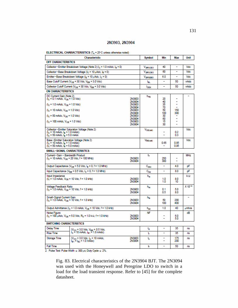
131
Fig. 83. Electrical characteristics of the 2N3904 BJT. The 2N3094
was used with the Honeywell and Peregrine LDO to switch in a
load for the load transient response. Refer to [45] for the complete
datasheet.
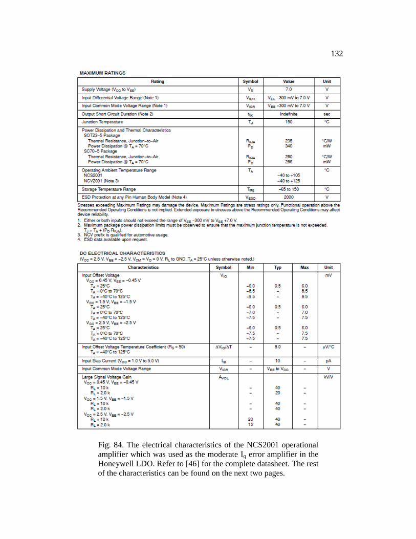
132
Fig. 84. The electrical characteristics of the NCS2001 operational
amplifier which was used as the moderate Iq error amplifier in the
Honeywell LDO. Refer to [46] for the complete datasheet. The rest
of the characteristics can be found on the next two pages.
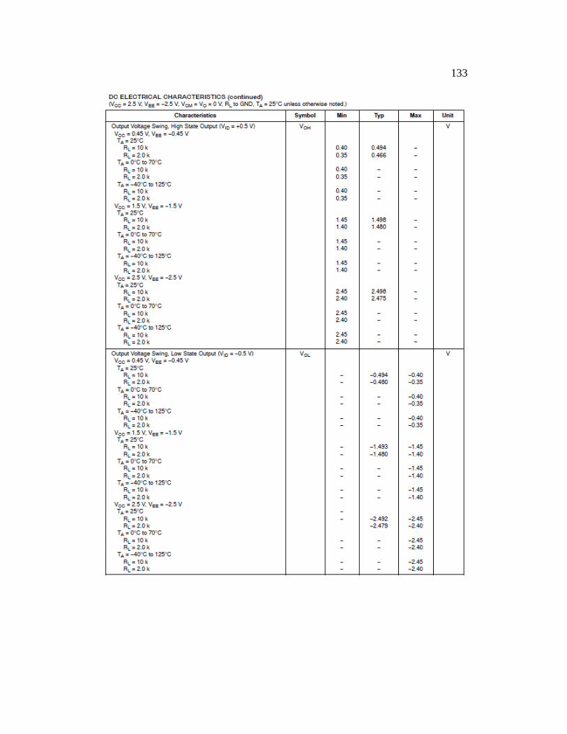
133

134

135
Fig. 85. The electrical characteristics of the LMP2231 operational
amplifier which was used as the low Iq error amplifier in the
Honeywell LDO. Refer to [47] for the complete datasheet.

136
APPENDIX B
BARE DIE PICTURE OF LARGE PASS DEVICE
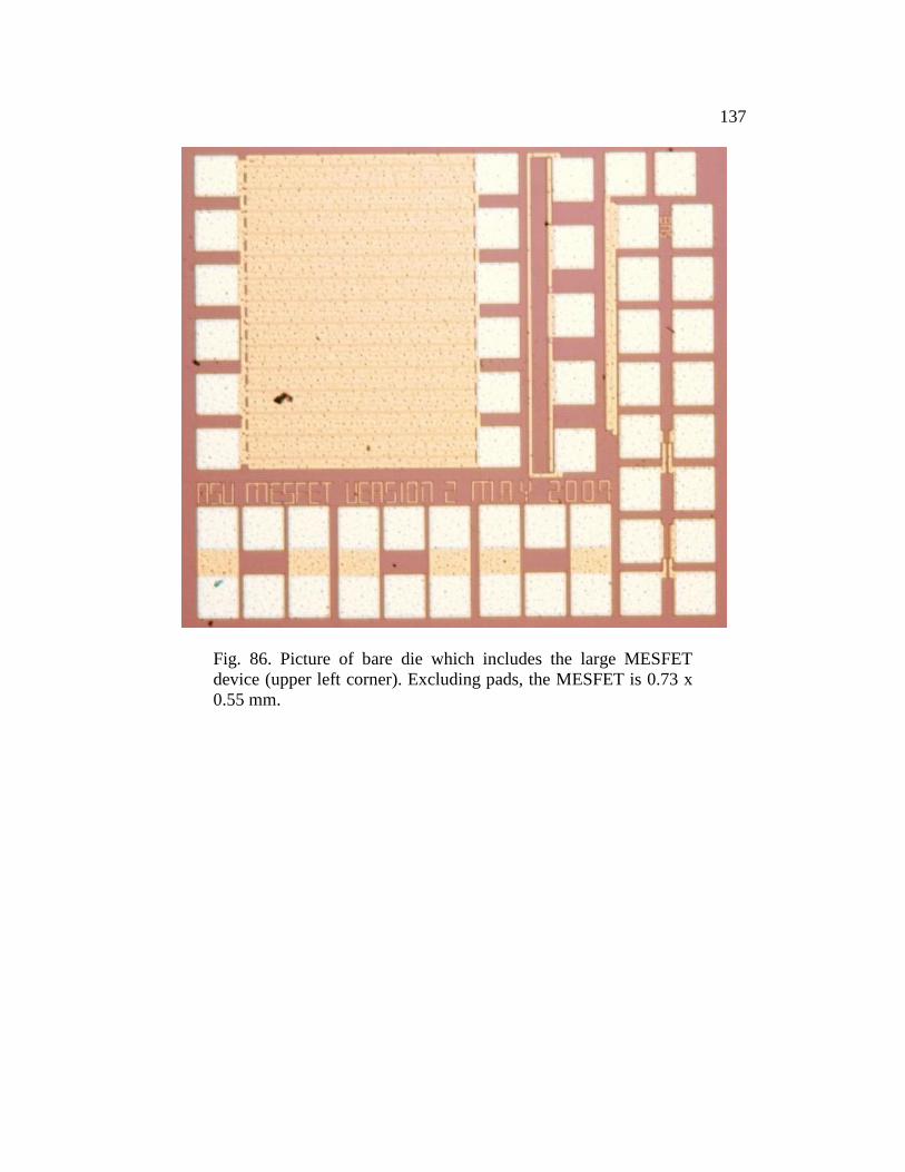
137
Fig. 86. Picture of bare die which includes the large MESFET
device (upper left corner). Excluding pads, the MESFET is 0.73 x
0.55 mm.

138
APPENDIX C
ADDITIONAL WIDE TEMPERATURE MEASUREMENTS FROM
HONEYWELL LDO
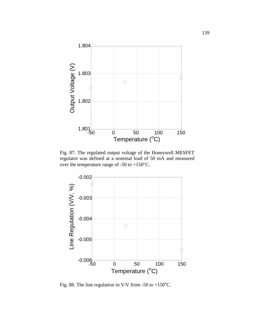
139
1.801
1.802
1.803
1.804
-50 0 50 100 150
Outp
ut V
oltage
(V
)
Temperature (oC)
Fig. 87. The regulated output voltage of the Honeywell MESFET
regulator was defined at a nominal load of 50 mA and measured
over the temperature range of -50 to +150C.
-0.006
-0.005
-0.004
-0.003
-0.002
-50 0 50 100 150
Lin
e R
eg
ula
tio
n (
V/V
, %
)
Temperature (oC)
Fig. 88. The line regulation in V/V from -50 to +150oC.
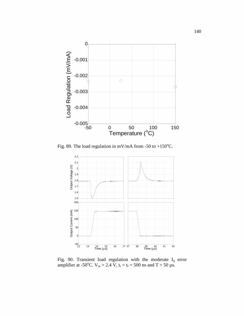
140
-0.005
-0.004
-0.003
-0.002
-0.001
0
-50 0 50 100 150
Lo
ad R
egu
lation
(m
V/m
A)
Temperature (oC)
Fig. 89. The load regulation in mV/mA from -50 to +150oC.
Fig. 90. Transient load regulation with the moderate Iq error
amplifier at -50oC. Vin = 2.4 V, tr = tf = 500 ns and T = 50 µs.
1.5
1.6
1.7
1.8
1.9
2
2.1
2.2
Outp
ut V
oltage
(V
)
-50
0
50
100
150
200
12 13 14 15 16 17
Outp
ut
Curr
en
t (m
A)
Time (s)37 38 39 40 41 42
Time (s)

141
Fig. 91. Transient load regulation with the moderate Iq error
amplifier at +150oC. Vin = 2.4 V, tr = tf = 500 ns and T = 50 µs.
Fig. 92. Transient line regulation with the moderate Iq error
amplifier at -50oC. Iout = 50 mA, tr = tf = 200 ns and T = 50 µs.
1
2
3
4
13 14 15 16 17 18
Input
Vo
ltage
(V
)
Time (s)
1.6
1.7
1.8
1.9
2
Outp
ut V
oltage
(V
)
38 39 40 41 42 43
Time (s)
1.5
1.6
1.7
1.8
1.9
2
2.1
2.2
Outp
ut V
oltage
(V
)
-50
0
50
100
150
200
11 12 13 14 15 16
Outp
ut C
urr
ent
(mA
)
Time (ms)
36 37 38 39 40 41
Time (ms)
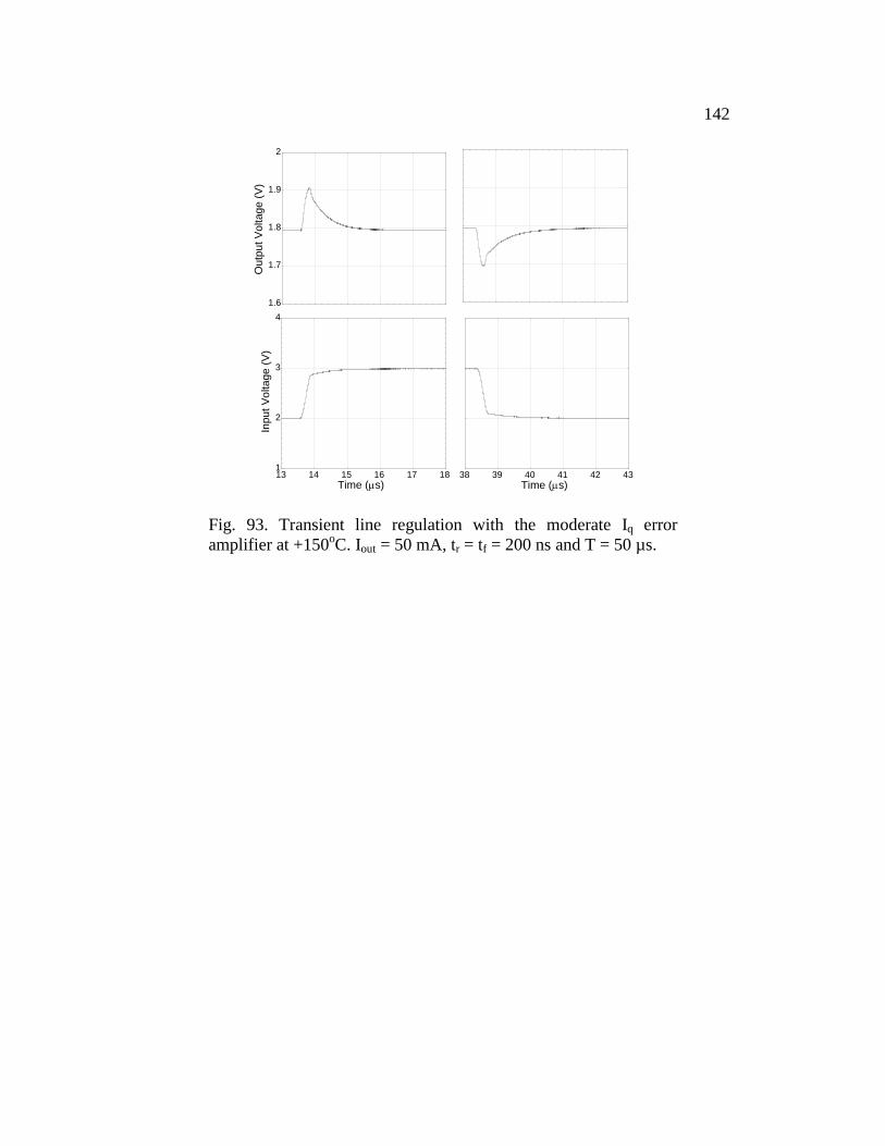
142
Fig. 93. Transient line regulation with the moderate Iq error
amplifier at +150oC. Iout = 50 mA, tr = tf = 200 ns and T = 50 µs.
1.6
1.7
1.8
1.9
2
Outp
ut V
oltage
(V
)
1
2
3
4
13 14 15 16 17 18
Inpu
t V
olta
ge
(V
)
Time (s)38 39 40 41 42 43
Time (s)

143
APPENDIX D
ADDITIONAL RADIATION MEASUREMENTS FROM HONEYWELL LDO
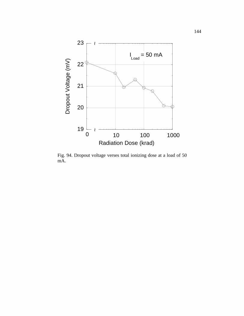
144
Fig. 94. Dropout voltage verses total ionizing dose at a load of 50
mA.
19
20
21
22
23
1 10 100 1000
Dro
po
ut
Vo
lta
ge
(m
V)
Radiation Dose (krad)
~~
ILoad
= 50 mA
0

145
Fig. 95. Transient line regulation with the moderate Iq error
amplifier after 1 Mrad(Si). Iout = 50 mA, tr = tf = 200 ns and T = 50
µs.
Fig. 96. Transient load regulation with the moderate Iq error
amplifier after 1 Mrad(Si). Vin = 2.4 V, tr = tf = 500 ns and T = 50
µs.
1.4
1.5
1.6
1.7
1.8
1.9
2
2.1
2.2
Outp
ut
Vo
lta
ge
(V
)
-50
0
50
100
150
200
8 9 10 11 12 13
Outp
ut
Cu
rren
t (m
A)
Time (s)32 33 34 35 36 37
Time (s)
1.5
1.6
1.7
1.8
1.9
2
Outp
ut
Volta
ge
(V
)
1
2
3
4
9 10 11 12 13 14
Inpu
t V
olta
ge
(V
)
Time (s)34 35 36 37 38 39
Time (s)

146
1.78
1.8
1.82
1.84
1.86
1.88
0 20 40 60 80 100
1 Mrad(Si)24 Hours of Annealing
Outp
ut V
oltage
(V
)
Output Current (mA)
Fig. 97. Load regulation comparing the MESFET LDO
immediately after 1 Mrad(Si) and after 24 hours of annealing.
1.6
1.7
1.8
1.9
2
1.6 1.8 2 2.2 2.4 2.6 2.8 3
1 Mrad(Si)24 Hours Of Annealing
Outp
ut
Vo
ltag
e (
V)
Input Voltage (V)
Fig. 98. Line regulation comparing the MESFET LDO
immediately after 1 Mrad(Si) and after 24 hours of annealing.

147
APPENDIX E
3-D LAYOUT OF THE PD-MESFET PASS TRANSISTOR
148
In this section, Google SketchUp [48] was used to create 3-D drawings to
better understand how the layout of the PD-MESFET (Fig. 86) contributed to the
operation of the MESFET. While it will not be completely shown here, the total
width of the PD-MESFET (119.28 mm) is broken up among 28 equal rows of
MESFETs with each row consisting of 426 fingers. Once again, a finger width of
10 µm was chosen since that was the finger size of the devices measured in
Chapter 2; however, that is by no means the optimal finger size. The 3-D layout
of two interdigitated fingers with widths of 10 µm can be seen in Fig. 99 and Fig.
100.
Fig. 101 shows a picture of 4 of the 28 rows as well as one of the drain
and source pads. With the exception of one pad in Fig. 86 being allocated for the
gate (fourth pad down on the left), all the pads to the left are for the drain and the
ones to the right are for the source. Only one pad was used for the gate since the
gate leakage is significantly smaller than the drain current and it does not affect
the dropout voltage. The bus lines for the drain run over the MESFETs fingers
and consists of metal layers 2 through 6 (M2-M6). The source and gate lines are
directly above and below the fingers and consist of all six metals layers (Fig.
102). Fig. 103 and Fig. 104 remove several of the metal lines and all but two of
the fingers to show how the MESFET connects to the bus lines.

149
Fig. 99. Layout of two interdigitated fingers.
Fig. 100. Shows a zoom in of Fig. 99.

150
Fig. 101. Shows 4 of the 28 rows in the PD-MESFET pass
transistor.
Fig. 102. Zooms in on one section of Fig. 101 to show the source,
drain, and gate lines.

151
Fig. 103. Removes the entire drain line and some of the metal
layers of the source and gate lines in Fig. 102 to show how
individual fingers connect to the bus lines. All but two of the
fingers were removed to simplify the picture.

152
Fig. 104. Shows a zoomed in picture of Fig. 103 as well the via
stack which connects the drain lines of the MESFET fingers (M1)
to the drain bus line (M2-M6).