Embed Size (px)
Citation preview
Optimization of sputtered titanium nitride as a tunable metal for plasmonic applications
Christine M. Zgrabik and Evelyn L. Hu* Harvard John A. Paulson School of Engineering and Applied Sciences, 9 Oxford St, Cambridge, MA 02138, USA
Abstract: Alternative materials for plasmonic devices have garnered much recent interest. A promising candidate material is titanium nitride. Although there is a substantial body of work on the formation of this material, its use for plasmonic applications requires a more systematic and detailed optical analysis than has previously been carried out. This paper describes an initial optimization of sputtered TiN thin films for plasmonic performance from visible into near-IR wavelengths. The metallic behavior of TiN films exhibits a sensitive dependence on the substrate and deposition details. We explored reactive and non-reactive sputter deposition of TiN onto various substrates at both room temperature and 600°C. Metallic character was compared for films grown under different conditions via spectroscopic ellipsometry and correlated with compositional and structural measurements via x-ray photoelectron spectroscopy (XPS), x-ray diffraction (XRD), and scanning transmission electron microscopy (STEM).
©2015 Optical Society of America
OCIS codes: (250.5403) Plasmonics; (240.2130) Ellipsometry and polarimetry; (240.6675) Surface photoemission and photoelectron spectroscopy; (310.6860) Thin films, optical properties; (310.1860) Deposition and fabrication.
References and links
1. G. V. Naik, V. M. Shalaev, and A. Boltasseva, “Alternative Plasmonic Materials: Beyond Gold and Silver,” Adv. Mater. 25(24), 3264–3294 (2013).
2. U. Guler, A. V. Kildishev, A. Boltasseva, and V. M. Shalaev, “Plasmonics on the slope of enlightenment: the role of transition metal nitrides,” Faraday Discuss. 178, 71–86 (2015).
3. G. Naik, J. Kim, and A. Boltasseva, “Oxides and nitrides as alternative plasmonic materials in the optical range,” Opt. Mater. Express 1(6), 1090–1099 (2011).
4. J. A. Dionne and H. A. Atwater, “Plasmonics: Metal-worthy methods and materials in nanophotonics,” MRS Bull. 37(08), 717–724 (2012).
5. J. T. Guske, J. Brown, A. Welsh, and S. Franzen, “Infrared surface plasmon resonance of AZO-Ag-AZO sandwich thin films,” Opt. Express 20(21), 23215–23226 (2012).
6. S. Franzen, “Surface Plasmon Polaritons and Screened Plasma Absorption in Indium Tin Oxide Compared to Silver and Gold,” J. Phys. Chem. C 112(15), 6027–6032 (2008).
7. F. H. L. Koppens, D. E. Chang, and F. J. García de Abajo, “Graphene Plasmonics: A Platform for Strong Light-Matter Interactions,” Nano Lett. 11(8), 3370–3377 (2011).
8. M. G. Blaber, M. D. Arnold, and M. J. Ford, “A review of the optical properties of alloys and intermetallics for plasmonics,” J. Phys. Condens. Matter 22(14), 143201 (2010).
9. U. Guler, A. Boltasseva, and V. M. Shalaev, Science 344, 263–264 (2014). 10. D. Steinmiller-Nethl, R. Kovacs, E. Gornik, and P. Rodhammer, “Excitation of surface plasmons on titanium
nitride films:determination of the dielectric function,” Thin Solid Films 237(1-2), 277–281 (1994).11. A. Boltasseva and H. A. Atwater, “Materials science. Low-Loss Plasmonic Metamaterials,” Science 331(6015),
290–291 (2011). 12. N. C. Chen, W. C. Lien, C. R. Liu, Y. L. Huang, Y. R. Lin, C. Chou, S. Y. Chang, and C. W. Ho, “Excitation of
surface plasma wave at TiN/air interface in the Kretschmann geometry,” J. Appl. Phys. 109(4), 043104 (2011).13. G. V. Naik, J. L. Schroeder, X. Ni, A. V. Kildishev, T. D. Sands, and A. Boltasseva, “Titanium nitride as a
plasmonic material for visible and near-infrared wavelengths,” Opt. Mater. Express 2(4), 478–489 (2012).14. U. Guler, G. V. Naik, A. Boltasseva, V. M. Shalaev, and A. V. Kildishev, “Performance analysis of nitride
alternative plasmonic materials for localized surface plasmon applications,” Appl. Phys. B 107(2), 285–291(2012).
#246076 Received 16 Jul 2015; revised 29 Oct 2015; accepted 2 Nov 2015; published 9 Nov 2015 © 2015 OSA 1 Dec 2015 | Vol. 5, No. 12 | DOI:10.1364/OME.5.002786 | OPTICAL MATERIALS EXPRESS 2786
15. W. Li, U. Guler, N. Kinsey, G. V. Naik, A. Boltasseva, J. Guan, V. M. Shalaev, and A. V. Kildishev, “Refractory Plasmonics with Titanium Nitride: Broadband Metamaterial Absorber,” Adv. Mater. 26(47), 7959–7965 (2014).
16. G. V. Naik, B. Saha, J. Liu, S. M. Saber, E. A. Stach, J. M. K. Irudayaraj, T. D. Sands, V. M. Shalaev, and A. Boltasseva, “Epitaxial superlattices with titanium nitride as a plasmonic component for optical hyperbolic metamaterials,” Proc. Natl. Acad. Sci. U.S.A. 111(21), 7546–7551 (2014).
17. H. Do, Y.-H. Wu, V.-T. Dai, C.-Y. Peng, T.-C. Yen, and L. Chang, “Structure and property of epitaxial titanium oxynitride grown on MgO(001) substrate by pulsed laser deposition,” Surf. Coat. Tech. 214, 91–96 (2013).
18. B. O. Johansson, J. E. Sundgren, J. E. Greene, A. Rockett, and S. A. Barnett, “Growth and properties of single crystal TiN films deposited by reactive magnetron sputtering,” J. Vac. Sci. Technol. A 3(2), 303–307 (1985).
19. P. H. Mayrhofer, F. Kunc, J. Musil, and C. Mitterer, “A comparative study on reactive and non-reactive unbalanced magnetron sputter deposition of TiN coatings,” Thin Solid Films 415(1-2), 151–159 (2002).
20. M. C. Biesinger, L. W. M. Lau, A. R. Gerson, and R. St. C. Smart, “Resolving surface chemical states in XPS analysis of first row transition metals, oxides and hydroxies: Sc, Ti, V, Cu and Zn,” Appl. Surf. Sci. 257(3), 887–898 (2010).
21. M. Delfino, J. A. Fair, and D. Hodu, “Xray photoemission spectra of reactively sputtered TiN,” J. Appl. Phys. 71(12), 6079 (1992).
22. C.-L. Liang, G.-A. Cheng, R.-T. Zheng, H.-P. Liu, J.-C. Li, H.-F. Zhang, G.-J. Ma, and Y.-L. Jiang, “Composition and texture of TiN thin films fabricated by ECR enhanced sputtering deposition,” Surf. Coat. Tech. 201(9-11), 5537–5540 (2007).
23. A. P. Hibbins, J. R. Sambles, and C. R. Lawrence, “Surface plasmon-polariton study of the optical dielectricfunction of titanium nitride,” J. Mod. Opt. 45(10), 2051–2062 (1998).
24. N. White, A. L. Campbell, J. T. Grant, R. Pachter, K. Eyink, R. Jakubiak, G. Martinez, and C. V. Ramana, “Surface/interface analysis and optical properties of RF sputter-deposited nanocrystalline titanium nitride thin films,” Appl. Surf. Sci. 292, 74–85 (2014).
25. P. Patsalas and S. Logothetidis, “Optical, electronic, and transport properties of nanocrystalline titanium nitride thin films,” J. Appl. Phys. 90(9), 4725–4734 (2001).
26. S. Adachi and M. Takahashi, “Optical properties of TiN films deposited by direct current reactive sputtering,” J. Appl. Phys. 87(3), 1264–1269 (2000).
27. F. Chen, S.-W. Wang, L. Yu, X. Chen, and W. Lu, “Control of optical properties of TiNxOy films and applicationfor high performance solar selective absorbing coatings,” Opt. Mater. Express 4(9), 1833–1847 (2014).
28. J. H. Kang and K. J. Kim, “Structural, optical, and electronic properties of cubic TiN x compounds,” J. Appl. Phys. 86(1), 346–350 (1999).
29. B. Karlsson, R. P. Shimshock, B. O. Seraphin, and J. C. Haygarth, “Optical Properties of CVD-Coated TiN, ZrN and HfN,” Phys. Scr. 25(6A), 775–779 (1982).
30. P. Patsalas, N. Kalfagiannis, and S. Kassavetis, “Optical Properties and Plasmonic Performance of Titanium Nitride,” Materials (Basel) 8(6), 3128–3154 (2015).
31. J. Rivory, J. M. Behaghel, S. Berthier, and J. Lafait, “Optical Properties of Substoichiometric TiNx,” Thin SolidFilms 78(2), 161–165 (1981).
32. S. T. Sundari, R. Ramaseshan, F. Jose, S. Dash, and A. K. Tyagi, “Investigation of temperature dependent dielectric constant of a sputtered TiN thin film by spectroscopic ellipsometry,” J. Appl. Phys. 115(3), 033516(2014).
33. P. B. Johnson and R. W. Christy, “Optical Constants of the Noble Metals,” Phys. Rev. B 6(12), 4370–4379(1972).
34. J. Narayan, P. Tiwari, X. Chen, J. Singh, R. Chowdhury, and T. Zheleva, “Epitaxial growth of TiN films on(100) silicon substrates by laser physical vapor deposition,” Appl. Phys. Lett. 61(11), 1290–1292 (1992).
35. L.-J. Meng and M. P. dos Santos, “Characterization of titanium nitride films prepared by d.c. reactive magnetron sputtering at different nitrogen pressures,” Surf. Coat. Tech. 90(1-2), 64–70 (1997).
36. J. A. Thornton, “The microstructure of sputter-deposited coatings,” J. Vac. Sci. Technol. A 4(6), 3059–3065(1986).
37. A. Anders, “A structure zone diagram including plasma-based deposition and ion etching,” Thin Solid Films518(15), 4087–4090 (2010).
38. A. Tarniowy, R. Mania, and M. Rekas, “The effect of thermal treatment on the structure, optical and electrical properties of amorphous titanium nitride thin films,” Thin Solid Films 311(1-2), 93–100 (1997).
39. C. Ernsberger, J. Nickerson, T. Smith, A. E. Miller, and D. Banks, “Low temperature oxidation behavior of reactively sputtered TiN by xray photoelectron spectroscopy and contact resistance measurements,” J. Vac. Sci. Technol. A 4(6), 2784–2788 (1986).
40. P. Prieto and R. E. Kirby, “Xray photoelectron spectroscopy study of the difference between reactively evaporated and direct sputterdeposited TiN films and their oxidation properties,” J. Vac. Sci. Technol. A 13(6),2819–2826 (1995).
41. N. C. Saha and H. G. Tompkins, “Titanium nitride oxidation chemistry: An xray photoelectron spectroscopy study,” J. Appl. Phys. 72(7), 3072–3079 (1992).
42. T. P. Thorpe, A. A. Morrish, and S. B. Qadri, “Effect of grain size on the oxidation kinetics of sputtered titanium nitride films,” J. Vac. Sci. Technol. A 6(3), 1727–1729 (1988).
43. M. J. Vasile, A. B. Emerson, and F. A. Baiocchi, “The characterization of titanium nitride by x‐ray photoelectron spectroscopy and Rutherford backscattering,” J. Vac. Sci. Technol. A 8(1), 99–105 (1990).
#246076 Received 16 Jul 2015; revised 29 Oct 2015; accepted 2 Nov 2015; published 9 Nov 2015 © 2015 OSA 1 Dec 2015 | Vol. 5, No. 12 | DOI:10.1364/OME.5.002786 | OPTICAL MATERIALS EXPRESS 2787

44. N. Saoula, K. Henda, and R. Kesri, “Influence of Nitrogen Content on the Structural and Mechanical Propertiesof TiN Thin Films,” J. Plasma Fusion Res. Series 8, 1403–1407 (2009).
45. S. Ohya, B. Chiaro, A. Megrant, C. Neill, R. Barends, Y. Chen, J. Kelly, D. Low, J. Mutus, P. J. J. O’Malley, P. Roushan, D. Sank, A. Vainsencher, J. Wenner, T. C. White, Y. Yin, B. D. Schultz, C. J. Palmstrøm, B. A. Mazin,A. N. Cleland, and J. M. Martinis, “Sputtered TiN films for superconducting coplanar waveguide resonators,” arXiv:1306.2966 (2013).
46. L. Wen and R. Huang, “Low Temperature Deposition of Titanium Nitride,” J. Mater. Sci. Technol. 14, 289–293(1998).
1. Introduction
Alternative metallic materials for plasmonic devices have been gaining popularity recently since they have some distinct advantages compared to the commonly used noble metals silver and gold [1–8]. The high hardness, chemical stability, high temperature performance [9], and potential CMOS-compatibility of titanium nitride (TiN) are desirable material attributes in the formation of robust plasmonic device structures. The optimal choice of material also depends on the operating wavelength of interest. TiN has been identified as an excellent candidate material for the visible and near-IR wavelength range [10–16] and unlike noble metals, has optical properties which are tunable.
Sputtered thin films of TiN exhibit varied mechanical [17–19], structural [17, 18, 20–22], and optical behavior [23–29]. A recent review highlights the optical studies of TiN prior to this study showing a wide range of behavior [30]. Understanding how to control the films over this wide, tunable range is advantageous in optimizing the plasmonic behavior of TiN. Our goal is to sputter what we term more “metallic” TiN, which we define as TiN with the negative real component of the permittivity maximized. This is a definition of “metallic” that pertains specifically to plasmonic applications, and it is this definition of “metallic” that we will employ throughout this paper. Thus “more metallic behavior” implies a greater value of the negative real component of the permittivity. This paper describes the critical sputter-deposition parameters of TiN thin films, and correlates those parameters with the changes in negative real permittivity of the films, so that we can predictably control these values from visible into IR wavelengths.
2. Experimental
Reactive and non-reactive sputter deposition was systematically carried out on silicon, sapphire, and MgO substrates. Films were deposited under various conditions with the goal of maximizing the magnitude of the real part of the permittivity, a descriptor of the metallic character of the film. The primary assessment of the metallic character was therefore carried out using spectroscopic ellipsometry, though results were also correlated with Hall resistivity, XPS, XRD, and STEM measurements to allow us to generate initial ideas as to the underlying reason for the ellipsometric differences we measure. TiN thin films displaying a full range of behavior from dielectric to metallic were produced. We found that the most important factors in achieving metallic TiN films suitable for plasmonics were the deposition temperature and applied substrate bias. In addition, the optical properties depended on the substrate and could be more finely tuned by adjusting the reactive gas composition.
Films were DC reactively magnetron sputtered using 2” diameter Ti targets in an AJA International ATC 2200-V load-locked turbo pumped sputtering system. To remove any residual surface oxide or contaminants from the Ti target, the target was pre-sputtered with the shutter closed until the voltage stabilized. A substrate heater controlled the temperature up to 600°C. The base pressure was less than 5 x 10⁻⁷ Torr after heating the substrate to 600°C and was in the 10−8 Torr range at room temperature. The deposition pressure was held constant at 4mT. The Ar: N2 gas flow ratio was systematically varied from nitrogen-deficient 12:4 sccm to nitrogen-dense 8:12 sccm for the reactively sputtered samples, monitored through mass flow controllers. For some films, as noted, a substrate bias of 100V was applied.
#246076 Received 16 Jul 2015; revised 29 Oct 2015; accepted 2 Nov 2015; published 9 Nov 2015 © 2015 OSA 1 Dec 2015 | Vol. 5, No. 12 | DOI:10.1364/OME.5.002786 | OPTICAL MATERIALS EXPRESS 2788

Additional films were non-reactively RF sputtered using a TiN target in a 40sccm Ar environment, with no N2 gas flow. The optical properties of these non-reactively formed films were directly compared with those of the reactively sputtered films. The substrates included (100) MgO, c-plane sapphire, and (100) p-silicon. Before being loaded into the chamber, all substrates were sonicated in acetone followed by isopropyl alcohol and N2 dried. Prior to this, Si substrates were additionally cleaned in a 49% HF dip with DI H2O rinse and N2 dry.
After deposition, the optical constants of the TiN films were measured from 300 to 1700 nm in 5nm steps using a J.A.Woollam WVASE32 spectroscopic ellipsometer. The measured permittivity (where ε = ε̍ + i ε̍ ̍) values varied from completely dielectric behavior (ε̍ > 0) over the entire range to metallic behavior (ε̍ < 0) for all wavelengths greater than about 500nm. We correlated these dramatic changes in optical behavior with methodical changes in the deposition conditions and film structure. The optical constants of the films were best modeled via Drude-Lorentz models [24, 30–32] consisting of one Drude term representing the free d-band conduction electrons and two Lorentz terms representing the interband losses similar to those exhibited by gold. The ellipsometric measurements were corroborated by Hall DC resistivity and XPS measurements. STEM and XRD measurements of metallic films showed a range of short range to long range crystalline order.
3. Results
As a general trend, those TiN films identified by spectroscopic ellipsometry to have a larger magnitude of negative real permittivity (i.e. were “more metallic”) also exhibited lower values of Hall resistivity, had a lower concentration of oxygen impurities, and exhibited better crystallinity. The most metallic films grown at elevated temperature showed textured epitaxial growth with strongly preferred orientation while the most metallic films grown at room temperature with an additional applied bias were textured with small crystallites. Films determined to be ‘dielectric’ through ellipsometric measurements exhibited high oxygen impurity concentrations and no discernible long-term crystalline order.
Fig. 1. (a) The real part of the permitivvity (ε) for various TiN films compared to silver and gold. The shaded area is bordered on top by the most dielectric and on bottom, most metallic films we have sputtered, demonstrating the wide range over which the optical character of reactively sputtered TiN can be tuned. (b) The imaginary part of the permittivity (losses) is shown. Data for Au and Ag adapted from Johnson & Christy [33].
Figure 1 shows sample traces of both the real and imaginary parts of the permitiviity (ε̍ and ε̍ )̍ of a selection of our sputtered TiN films as a function of wavelength. Our TiN films are compared to the bulk values from literature for standard plasmonic metals, silver and gold [33]. We can controllably tune the optical properties of the sputtered TiN throughout the shaded range in the figure to be dielectric or metallic over most of the visible and near-IR wavelength range. Since we are interested in metallic TiN specifically for plasmonic
#246076 Received 16 Jul 2015; revised 29 Oct 2015; accepted 2 Nov 2015; published 9 Nov 2015 © 2015 OSA 1 Dec 2015 | Vol. 5, No. 12 | DOI:10.1364/OME.5.002786 | OPTICAL MATERIALS EXPRESS 2789
applications, this study highlights the conditions necessary to deposit metallic TiN films with maximum negative ε̍ . We focus on the real part of the permittivy throughout; in general, as the oxygen impurity concentration is lowered and the crystallinity improves, the ε̍ becomes more negative and ε̍ ̍ also decreases. This can be seen by comparing the ‘intermediate’ and ‘metallic’ TiN curves in Fig. 1.
As discussed below, the substrate temperature, substrate choice, amount of N2 gas flow, and any additional applied bias all had significant effects on the optical properties of the final films. We found that varying the composition of gases during reactive sputtering of TiN in general gave a greater degree of control to the thin film formation as compared to nonreactive sputtering; however, by varying the substrate temperature during deposition, a significant range of properties can also be achieved via nonreactive sputtering. In addition, by applying a bias while sputtering we were able to deposit metallic TiN films at room temperature.
Since we found that the deposition temperature had the overall greatest influence on the metallic nature of high quality TiN, we will begin by discussing this parameter followed by the effects of the substrate choice. We will then evaluate the changes due to gas composition in reactive sputtering as compared to non-reactive sputtering for a particular substrate, since these effects are more interactive. We will finish by examining the metallic films produced at room temperature with the addition of a substrate bias. Finally, we will discuss the results including correlations of the optical behavior with structure and composition measurements to provide initial suggestions as to the underlying structural cause of the variation in optical properties.
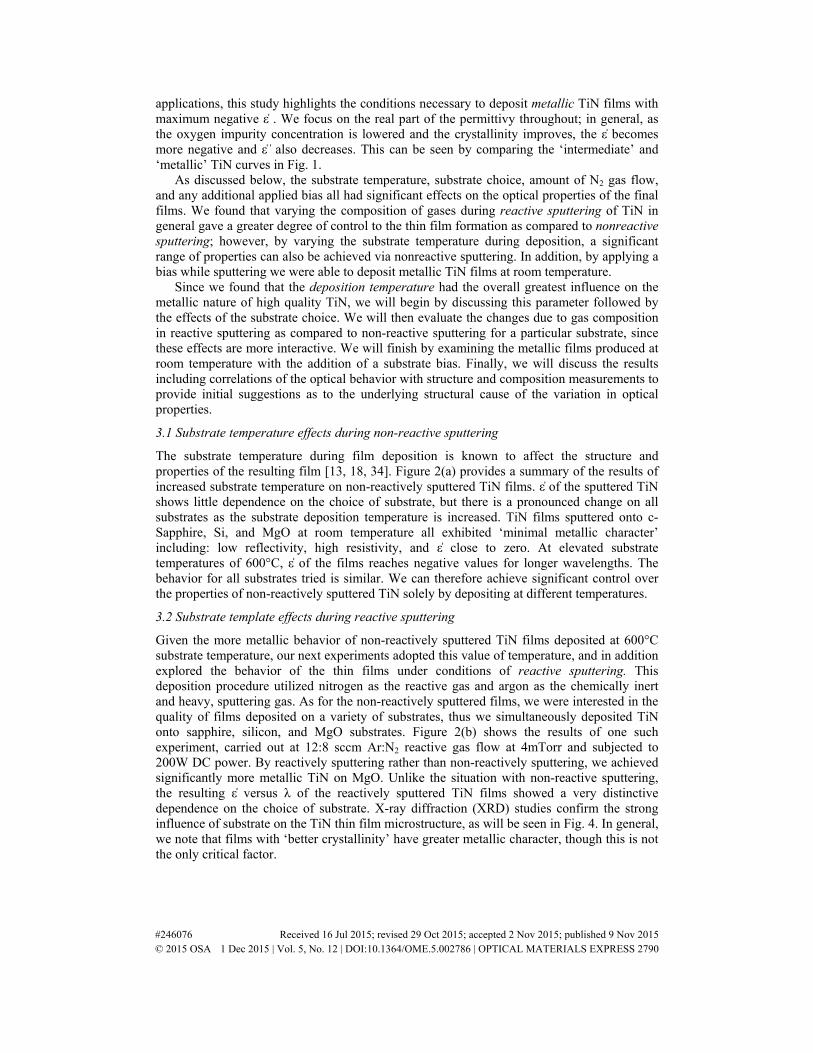
3.1 Substrate temperature effects during non-reactive sputtering
The substrate temperature during film deposition is known to affect the structure and properties of the resulting film [13, 18, 34]. Figure 2(a) provides a summary of the results of increased substrate temperature on non-reactively sputtered TiN films. ε̍ of the sputtered TiN shows little dependence on the choice of substrate, but there is a pronounced change on all substrates as the substrate deposition temperature is increased. TiN films sputtered onto c-Sapphire, Si, and MgO at room temperature all exhibited ‘minimal metallic character’ including: low reflectivity, high resistivity, and ε̍ close to zero. At elevated substrate temperatures of 600°C, ε̍ of the films reaches negative values for longer wavelengths. The behavior for all substrates tried is similar. We can therefore achieve significant control over the properties of non-reactively sputtered TiN solely by depositing at different temperatures.
3.2 Substrate template effects during reactive sputtering
Given the more metallic behavior of non-reactively sputtered TiN films deposited at 600°C substrate temperature, our next experiments adopted this value of temperature, and in addition explored the behavior of the thin films under conditions of reactive sputtering. This deposition procedure utilized nitrogen as the reactive gas and argon as the chemically inert and heavy, sputtering gas. As for the non-reactively sputtered films, we were interested in the quality of films deposited on a variety of substrates, thus we simultaneously deposited TiN onto sapphire, silicon, and MgO substrates. Figure 2(b) shows the results of one such experiment, carried out at 12:8 sccm Ar:N2 reactive gas flow at 4mTorr and subjected to 200W DC power. By reactively sputtering rather than non-reactively sputtering, we achieved significantly more metallic TiN on MgO. Unlike the situation with non-reactive sputtering, the resulting ε̍ versus λ of the reactively sputtered TiN films showed a very distinctive dependence on the choice of substrate. X-ray diffraction (XRD) studies confirm the strong influence of substrate on the TiN thin film microstructure, as will be seen in Fig. 4. In general, we note that films with ‘better crystallinity’ have greater metallic character, though this is not the only critical factor.
#246076 Received 16 Jul 2015; revised 29 Oct 2015; accepted 2 Nov 2015; published 9 Nov 2015 © 2015 OSA 1 Dec 2015 | Vol. 5, No. 12 | DOI:10.1364/OME.5.002786 | OPTICAL MATERIALS EXPRESS 2790
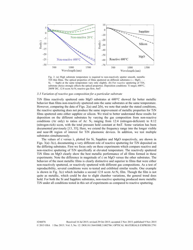
Fig. 2. (a) High substrate temperature is required to non-reactively sputter smooth, metallic TiN thin films. The optical properties of films sputtered on different substrates (— MgO, – – Si, ··· Saph) at the same temperature vary only slightly. (b) For reactive sputtering of TiN, substrate choice strongly affects the optical properties. Deposition conditions: Ti target, 600°C, 200W DC, 12:8 sccm Ar:N2 reactive gas flow, 4mT
3.3 Variation of reactive gas composition for a particular substrate
TiN films reactively sputtered onto MgO substrates at 600°C showed far better metallic behavior than films non-reactively sputtered onto the same substrates at the same temperature. However, comparing the data of Figs. 2(a) and 2(b), we note that under the stated conditions, the reactive sputtering does not produce the same improvement of metallic properties for TiN films sputtered onto either sapphire or silicon. We tried to better understand these results for deposition on the different substrates by varying the gas composition from non-reactive conditions (Ar only) to ratios of Ar: N2 ranging from 12:4 (nitrogen-deficient) to 8:12 (nitrogen-rich) sccm, with the total pressure held constant at 4mT. Some variation has been documented previously [13, 35]; Here, we extend the frequency range into the longer visible and near-IR region of interest for TiN plasmonic devices. In addition, we test multiple substrates simultaneously.
The values of ε̍ versus λ, plotted for Si, Sapphire and MgO respectively, are shown in Figs. 3(a)–3(c), documenting a very different role of reactive sputtering for TiN deposited on the differing substrates. First we focus only on these experiments which compare reactive and non-reactive sputtering of TiN specifically at elevated temperature. The reactively sputtered TiN films on MgO clearly show the best metallic performance of all films formed in these experiments. Note the difference in magnitude of ε̍ on MgO versus the other substrates. The behavior of the most metallic films is clearly distinctive and superior to films that were either non-reactively sputtered, or reactively sputtered with different gas compositions. As a test of reproducibility, several conditions were re-tested and exhibited similar results. One example is shown in Fig. 3(c) which includes a second 12:8 sccm Ar:N2 film. Though the film is not quite as metallic, which could be due to slight chamber variations, the general trend does hold. For both the Si and Sapphire substrates, non-reactive sputtering produced more metallic TiN under all conditions tested in this set of experiments as compared to reactive sputtering.
#246076 Received 16 Jul 2015; revised 29 Oct 2015; accepted 2 Nov 2015; published 9 Nov 2015 © 2015 OSA 1 Dec 2015 | Vol. 5, No. 12 | DOI:10.1364/OME.5.002786 | OPTICAL MATERIALS EXPRESS 2791

Fig. 3. Finer control during reactive sputtering is achieved by varying the reactive gas concentration. TiN films are deposited at 600°C (a–c) or 20°C plus an additional 100V bias (d–f), with varying amounts of Ar:N2 gas (sccm) Substrates are (a,d) silicon (b,e) sapphire (c,f) MgO. Reactive sputtering onto MgO substrates can produce highly metallic, epitaxial films. Non-reactive sputtering produced the most metallic films on Si and Sapphire.
3.4 Additional substrate bias for metallic films sputtered at room temperature
Low temperature deposition of metallic TiN is crucial for CMOS compatibility. The discussion so far has assumed that high temperature was necessary to sputter metallic TiN; however, films with large magnitudes of negative real epsilon can also be sputtered by applying an additional substrate bias. As shown in Figs. 3(e)–3(f), drastic improvements in metallic character of TiN films sputtered onto sapphire substrates, even at room temperature, can be achieved with the addition of a 100V bias. In addition, highly metallic TiN films are also sputtered onto MgO at room temperature whereas previously, elevated temperature was required. The drawback to this method is that films sputtered with the additional bias tend to be slightly rougher and have more defects than films sputtered at elevated temperatures. These initial results suggest, however, that CVD or ALD deposition of metallic TiN films, for example, is also likely possible at low temperature with proper optimization and additionally, allow for plasmonic-quality TiN deposition on a larger variety of substrates.
4. Discussion
Structure zone diagrams (SZD) help us to qualitatively organize the expected microstructures of deposited films from porous to columnar to granular. They also offer suggestions for process adjustments when we deposit films which have undesired properties. One of the most commonly used diagrams by Thornton [36], which refers specifically to sputtered films, includes two main axes affecting the film microstructure outcome: the deposition pressure and the fraction T/Tm of the deposition temperature, T, over the melting temperature, Tm of the deposited film. His diagram posits that as T/Tm increases, films tend to have lower porosity and larger grain sizes. Thornton acknowledges that at the temperatures that we work with in this study, there are several parameters influencing the surface morphology. Our TiN films deposited at 600°C have small crystallites (< 50nm), high reflectivity, and low oxygen incorporation. These results are also supported by additional experiments from the literature [13, 18]. On the other hand, TiN films deposited at low temperature have low reflectivity,
#246076 Received 16 Jul 2015; revised 29 Oct 2015; accepted 2 Nov 2015; published 9 Nov 2015 © 2015 OSA 1 Dec 2015 | Vol. 5, No. 12 | DOI:10.1364/OME.5.002786 | OPTICAL MATERIALS EXPRESS 2792

high resisitivity and high oxygen incorporation, potentially due to a film porosity which encourages oxidation upon removal from vacuum to ambient. Our low temperature films are always non-metallic unless additional energy is added during the deposition, such as a substrate bias.
A more recent structure zone diagram proposes that the Thornton axes be replaced by generalized temperature T* and normalized energy E* axes [37]. Anders’ model suggests that the new E* axis include all parameters which contribute to the kinetic energy of ions arriving at the substrate, for example: deposition pressure, applied plasma voltage, and substrate bias. Our metallic TiN films deposited at room temperature with a substrate bias fit well into this model. Due to the added bias, the adatoms have enough energy upon arrival at the substrate to rearrange on the surface. In addition, an applied bias may re-sputter some of the already deposited TiN film. Our films with applied bias exhibit lower oxygen content, perhaps due to preferential sputtering of the oxygen from the surface, or from adatom rearrangement upon re-sputtering.
Reactive sputtering involves many complex reactions and it is quite difficult to fully understand the details of these processes; however, beyond studying the microstructure, additional understanding may be gained through compositional and structural measurements on a selection of our sputtered TiN films. We have used X-ray diffraction (XRD), X-ray photoelectron spectroscopy (XPS) and scanning transmission electron microscopy (STEM) in an attempt to formulate initial suggestions as to the underlying factors in sputtering metallic TiN. We hypothesize that the two main factors influencing the optical behavior of sputtered TiN films are the crystallinity, as well as the composition of the film, which includes both the stoichiometry and the oxygen impurity concentration.
Beyond the influences of elevated temperature or applied bias on the film quality, our data suggest the importance of the substrate as a template for the TiN in determining its structure and stoichiometry. This is evidenced in the dramatic improvement of TiN films specifically on MgO via reactive as compared to nonreactive sputtering shown in Fig. 3, as well as the distinctive differences in ε versus λ for the different substrates. Since many of our ‘most metallic’ films were sputtered onto MgO, we focus on TiN films on this substrate to investigate structural and composition changes. With proper optimization of the chamber conditions, highly textured and even epitaxial growth of TiN on MgO can occur since MgO and stoichiometric TiN are closely lattice matched cubic crystals with lattice constants of 4.212 and 4.240 Å respectively [16–18]. It has been shown that crystalline TiN films exhibit metallic behavior whereas amorphous films do not [16, 38] and in fact, as we have noted, better crystallinity is, in general, correlated with the more metallic behavior we observe.
Anders’ generalized zone structure diagram suggests a small deposition parameter space where “low-temperature low-energy ion-assisted epitaxial growth” is possible [37]. By applying an additional substrate bias, we have shown that we can deposit metallic TiN at room temperature and we have also studied these films at the microstructural level. Figure 4 shows the previously studied high deposition temperature film (blue) as compared to a film deposited at room temperature with applied bias (red). Both films are textured, exhibiting XRD signatures only in the (200) direction. The film deposited at high temperature exhibits slightly better ordering, seen in the STEM images of those same films (see Figs. 5(b) and 5(c); colors are consistent in identifying films in Figs. 4 and 5).
#246076 Received 16 Jul 2015; revised 29 Oct 2015; accepted 2 Nov 2015; published 9 Nov 2015 © 2015 OSA 1 Dec 2015 | Vol. 5, No. 12 | DOI:10.1364/OME.5.002786 | OPTICAL MATERIALS EXPRESS 2793
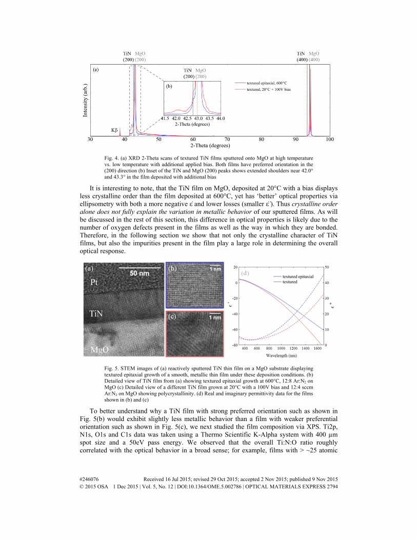
Fig. 4. (a) XRD 2-Theta scans of textured TiN films sputtered onto MgO at high temperature vs. low temperature with additional applied bias. Both films have preferred orientation in the (200) direction (b) Inset of the TiN and MgO (200) peaks shows extended shoulders near 42.0° and 43.3° in the film deposited with additional bias
It is interesting to note, that the TiN film on MgO, deposited at 20°C with a bias displays less crystalline order than the film deposited at 600°C, yet has ‘better’ optical properties via ellipsometry with both a more negative ε̍ and lower losses (smaller ε̍ ̍). Thus crystalline order alone does not fully explain the variation in metallic behavior of our sputtered films. As will be discussed in the rest of this section, this difference in optical properties is likely due to the number of oxygen defects present in the films as well as the way in which they are bonded. Therefore, in the following section we show that not only the crystalline character of TiN films, but also the impurities present in the film play a large role in determining the overall optical response.
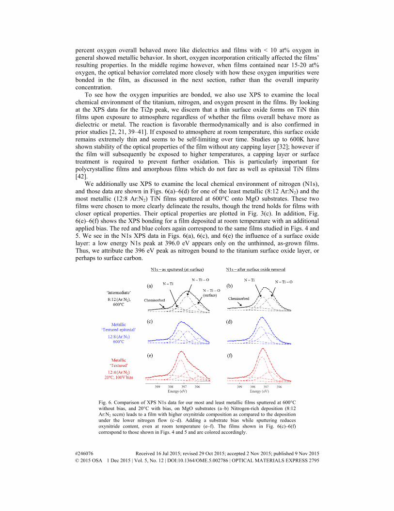
Fig. 5. STEM images of (a) reactively sputtered TiN thin film on a MgO substrate displaying textured epitaxial growth of a smooth, metallic thin film under these deposition conditions. (b) Detailed view of TiN film from (a) showing textured epitaxial growth at 600°C, 12:8 Ar:N2 on MgO (c) Detailed view of a different TiN film grown at 20°C with a 100V bias and 12:4 sccm Ar:N2 on MgO showing polycrystallinity. (d) Real and imaginary permittivity data for the films shown in (b) and (c)
To better understand why a TiN film with strong preferred orientation such as shown in Fig. 5(b) would exhibit slightly less metallic behavior than a film with weaker preferential orientation such as shown in Fig. 5(c), we next studied the film composition via XPS. Ti2p, N1s, O1s and C1s data was taken using a Thermo Scientific K-Alpha system with 400 µm spot size and a 50eV pass energy. We observed that the overall Ti:N:O ratio roughly correlated with the optical behavior in a broad sense; for example, films with > ~25 atomic
#246076 Received 16 Jul 2015; revised 29 Oct 2015; accepted 2 Nov 2015; published 9 Nov 2015 © 2015 OSA 1 Dec 2015 | Vol. 5, No. 12 | DOI:10.1364/OME.5.002786 | OPTICAL MATERIALS EXPRESS 2794
percent oxygen overall behaved more like dielectrics and films with < 10 at% oxygen in general showed metallic behavior. In short, oxygen incorporation critically affected the films’ resulting properties. In the middle regime however, when films contained near 15-20 at% oxygen, the optical behavior correlated more closely with how these oxygen impurities were bonded in the film, as discussed in the next section, rather than the overall impurity concentration.
To see how the oxygen impurities are bonded, we also use XPS to examine the local chemical environment of the titanium, nitrogen, and oxygen present in the films. By looking at the XPS data for the Ti2p peak, we discern that a thin surface oxide forms on TiN thin films upon exposure to atmosphere regardless of whether the films overall behave more as dielectric or metal. The reaction is favorable thermodynamically and is also confirmed in prior studies [2, 21, 39–41]. If exposed to atmosphere at room temperature, this surface oxide remains extremely thin and seems to be self-limiting over time. Studies up to 600K have shown stability of the optical properties of the film without any capping layer [32]; however if the film will subsequently be exposed to higher temperatures, a capping layer or surface treatment is required to prevent further oxidation. This is particularly important for polycrystalline films and amorphous films which do not fare as well as epitaxial TiN films [42].
We additionally use XPS to examine the local chemical environment of nitrogen (N1s), and those data are shown in Figs. 6(a)–6(d) for one of the least metallic (8:12 Ar:N2) and the most metallic (12:8 Ar:N2) TiN films sputtered at 600°C onto MgO substrates. These two films were chosen to more clearly delineate the results, though the trend holds for films with closer optical properties. Their optical properties are plotted in Fig. 3(c). In addition, Fig. 6(e)–6(f) shows the XPS bonding for a film deposited at room temperature with an additional applied bias. The red and blue colors again correspond to the same films studied in Figs. 4 and 5. We see in the N1s XPS data in Figs. 6(a), 6(c), and 6(e) the influence of a surface oxidelayer: a low energy N1s peak at 396.0 eV appears only on the unthinned, as-grown films. Thus, we attribute the 396 eV peak as nitrogen bound to the titanium surface oxide layer, or perhaps to surface carbon.
Fig. 6. Comparison of XPS N1s data for our most and least metallic films sputtered at 600°C without bias, and 20°C with bias, on MgO substrates (a–b) Nitrogen-rich deposition (8:12 Ar:N2 sccm) leads to a film with higher oxynitride composition as compared to the deposition under the lower nitrogen flow (c–d). Adding a substrate bias while sputtering reduces oxynitride content, even at room temperature (e–f). The films shown in Fig. 6(c)–6(f) correspond to those shown in Figs. 4 and 5 and are colored accordingly.
#246076 Received 16 Jul 2015; revised 29 Oct 2015; accepted 2 Nov 2015; published 9 Nov 2015 © 2015 OSA 1 Dec 2015 | Vol. 5, No. 12 | DOI:10.1364/OME.5.002786 | OPTICAL MATERIALS EXPRESS 2795
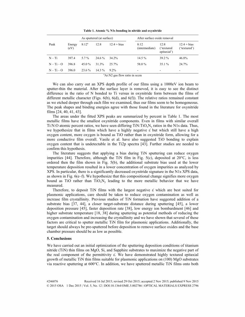
Table 1. Atomic % N1s bonding in nitride and oxynitride
As sputtered (at surface) After surface oxide removal
Peak Energy (eV)
8:12a 12:8 12:4 + bias 8:12 (intermediate)
12:8(‘textured epitaxial’)
12:4 + bias (‘textured’)
N – Ti 397.4 5.7 % 24.6 % 34.2% 14.5 % 39.2 % 46.8%
N – Ti – O 396.8 45.0 % 31.3% 25.7% 58.0 % 35.1 % 24.7%
N – Ti – O 396.0 23.6 % 14.3 % 9.2% - - - aAr:N2 gas flow ratio in sccm
We can also carry out an XPS depth profile of our films using a 1000eV ion beam to sputter-thin the material. After the surface layer is removed, it is easy to see the distinct difference in the ratio of N bonded to Ti versus in oxynitride form between the films of different metallic character (Figs. 6(b), 6(d), and 6(f)). The relative ratios remained constant as we etched deeper through each film we examined, thus our films seem to be homogeneous. The peak shapes and binding energies agree with those found in the literature for oxynitride films [24, 40, 41, 43].
The areas under the fitted XPS peaks are summarized by percent in Table 1. The most metallic films have the smallest oxynitride components. Even in films with similar overall Ti:N:O atomic percent ratios, we have seen differing TiN:TiOxNy ratios in the N1s data. Thus, we hypothesize that in films which have a highly negative ε̍ but which still have a high oxygen content, more oxygen is bound as TiO rather than in oxynitride form, allowing for a more conductive film overall. Vasile et al. have also suggested TiO bonding to explain oxygen content that is undetectable in the Ti2p spectra [43]. Further studies are needed to confirm this hypothesis.
The literature suggests that applying a bias during TiN sputtering can reduce oxygen impurities [44]. Therefore, although the TiN film in Fig. 5(c), deposited at 20°C, is less ordered then the film shown in Fig. 5(b), the additional substrate bias used at the lower temperature deposition resulted in a lower concentration of oxygen impurities as analyzed by XPS. In particular, there is a significantly decreased oxynitride signature in the N1s XPS data, as shown in Fig. 6(e–f). We hypothesize that this compositional change signifies more oxygen bound as TiO rather than TiOxNy leading to the more metallic behavior that we have measured.
Therefore, to deposit TiN films with the largest negative ε̍ which are best suited for plasmonic applications, care should be taken to reduce oxygen contamination as well as increase film crystallinity. Previous studies of TiN formation have suggested addition of a substrate bias [37, 44], a closer target-substrate distance during sputtering [45], a lower deposition pressure [45], faster deposition rate [38], low energy ion bombardment [46] and higher substrate temperature [18, 38] during sputtering as potential methods of reducing the oxygen contamination and increasing the crystallinity and we have shown that several of these factors are critical to sputter metallic TiN film for plasmonic applications. Additionally, the target should always be pre-sputtered before deposition to remove surface oxides and the base chamber pressure should be as low as possible.
5. Conclusions
We have carried out an initial optimization of the sputtering deposition conditions of titanium nitride (TiN) thin films on MgO, Si, and Sapphire substrates to maximize the negative part of the real component of the permittivity ε̍. We have demonstrated highly textured epitaxial growth of metallic TiN thin films suitable for plasmonic applications on (100) MgO substrates via reactive sputtering at 600°C. In addition, we have sputtered metallic TiN films onto both
#246076 Received 16 Jul 2015; revised 29 Oct 2015; accepted 2 Nov 2015; published 9 Nov 2015 © 2015 OSA 1 Dec 2015 | Vol. 5, No. 12 | DOI:10.1364/OME.5.002786 | OPTICAL MATERIALS EXPRESS 2796
MgO and Sapphire substrates at room temperature by applying an additional 100V substrate bias. While epitaxial growth of TiN on Si has been predicted via domain matching epitaxy [34], we have not seen this in our experiments and have produced TiN films of only moderate metallic character on Si substrates. The films with the most metallic character and lowest relative losses have been reactively sputtered on MgO substrates producing TiN films with strong preferential orientation which are suitable for applications requiring a visibly transparent substrate. Reactive sputtering of TiN does not seem to have an advantage over non-reactive sputtering on silicon or sapphire substrates for the conditions tested. In addition, previous studies have shown TiN with very low resistivity grown at even higher temperatures, in agreement with many structure zone models for sputtered films [18, 36, 37]. Therefore, further studies could include exploring deposition temperatures above 600°C to determine the limits of metallic character achievable via this method. Even more interesting would be deposition studies at elevated temperature with a small applied substrate bias to improve crystallinity as well as reduce oxygen impurities.
Acknowledgments
The authors would also like to acknowledge Dr. Andrew Magyar who prepared the lamellae and performed the STEM measurements. We also thank Dr. Shao-Liang Zheng from the X-Ray Laboratory in the Harvard University Department of Chemistry & Chemical Biology for his help with the X-ray data collection. This work was performed in part at the Center for Nanoscale Systems (CNS), a member of the National Nanotechnology Infrastructure Network (NNIN), which is supported by the National Science Foundation (NSF) under NSF award no. ECS-0335765. CNS is part of Harvard University.
#246076 Received 16 Jul 2015; revised 29 Oct 2015; accepted 2 Nov 2015; published 9 Nov 2015 © 2015 OSA 1 Dec 2015 | Vol. 5, No. 12 | DOI:10.1364/OME.5.002786 | OPTICAL MATERIALS EXPRESS 2797