Embed Size (px)
Citation preview

Ultramicroscopy 179 (2017) 57–62
Contents lists available at ScienceDirect
Ultramicroscopy
journal homepage: www.elsevier.com/locate/ultramic
Optimising multi-frame ADF-STEM for high-precision
atomic-resolution strain mapping
Lewys Jones a , ∗, Sigurd Wenner b , Magnus Nord
b , Per Harald Ninive
c , Ole Martin Løvvik
d , Randi Holmestad
b , Peter D. Nellist a
a Department of Materials, University of Oxford, Oxford, OX13PH, UK b Department of Physics, NTNU- Norwegian University of Science and Technology, Trondheim, NO-7491, Norway c NTNU- Norwegian University of Science and Technology, Gjøvik, NO-2815, Norway d SINTEF Materials and Chemistry, Oslo, NO-0314, Norway
a r t i c l e i n f o
Article history:
Received 5 August 2016
Revised 5 April 2017
Accepted 14 April 2017
Available online 15 April 2017
Keywords:
ADF-STEM
Experiment design
Strain in crystals/solids
Aluminium alloys
Density functional calculations
a b s t r a c t
Annular dark-field scanning transmission electron microscopy is a powerful tool to study crystal defects
at the atomic scale but historically single slow-scanned frames have been plagued by low-frequency
scanning-distortions prohibiting accurate strain mapping at atomic resolution. Recently, multi-frame ac-
quisition approaches combined with post-processing have demonstrated significant improvements in
strain precision, but the optimum number of frames to record has not been explored. Here we use a
non-rigid image registration procedure before applying established strain mapping methods. We deter-
mine how, for a fixed total electron-budget, the available dose should be fractionated for maximum strain
mapping precision. We find that reductions in scanning-artefacts of more than 70% are achievable with
image series of 20–30 frames in length. For our setup, series longer than 30 frames showed little fur-
ther improvement. As an application, the strain field around an aluminium alloy precipitate was studied,
from which our optimised approach yields data whos strain accuracy is verified using density functional
theory.
© 2017 Elsevier B.V. All rights reserved.
1
a
l
m
u
q
fl
d
c
s
t
i
m
n
N
n
S
e
t
i
t
d
q
v
t
t
i
t
t
g
c
t
b
i
a
h
0
. Introduction
The measurement of lattice distortion and strain in materi-
ls at the nanoscale presents an important characterisation chal-
enge. Strain is crucial in controlling the functional, electrical and
echanical properties of materials, and strain field design can
nlock the engineering of new material properties, including in
uantum-dots [1] , semiconductor transistors [2] , ferroelectrics [3] ,
exoelectrics [4] , high-temperature superconductors [5] and alloy
evelopment [6] . High-resolution electron microscopy techniques
an map strain information; however, the finite resolution and
ignal-to-noise ratio (SNR) of experimental images makes a quan-
itative measurement of these subtle displacements very challeng-
ng. Current experimental approaches include; conventional trans-
ission electron microscopy (CTEM) [7–9] , convergent-beam [10] ,
ano-beam [11] or nano-precession [12] electron diffraction (CBED,
BED, NPED), dark-field electron holography [13] (DFEH), and an-
ular dark-field scanning transmission electron microscopy (ADF-
TEM) [14–16] . Concise reviews of these methods can be found
∗ Corresponding author.
E-mail address: [email protected] (L. Jones).
e
[
a
ttp://dx.doi.org/10.1016/j.ultramic.2017.04.007
304-3991/© 2017 Elsevier B.V. All rights reserved.
lsewhere [17,18] ; but notably, each of these methods come with
heir own unique complications. With CTEM, careful choice of
maging parameters must be used to avoid image artefacts or con-
rast inversions from (for example) sample-tilt, sample-thickness,
efocus or aberration changes. CBED strain measurements can re-
uire significant sample tilt to achieve high-precision and can be
ulnerable to crystal plane bending, while DFEH, NBED and NPED
echniques each require additional hardware (a bi-prism, an addi-
ional condenser lens, and precession coils respectively) and more
nvolved off-line data processing. Lastly, in STEM the serial na-
ure of the image raster means that environmental effects can dis-
ort the image fidelity [19–21] and the necessary atomic resolution
enerally requires aberration correction.
Of the methods above, there has been increased interest re-
ently in measuring strain from ADF-STEM images to make use of
heir Z-contrast and incoherent nature. The development of high-
rightness electron sources and aberration correctors has improved
mage-resolution, while improvements in power-supply stability
nd acoustic isolation [19] have reduced problems from 50(60) Hz
lectrical, and few-kHz acoustic, scan-noise artefacts respectively
20,22] . As a result, and taking the nomenclature from [21] , our
ttention now turns to the far harder to isolate low-frequency
58 L. Jones et al. / Ultramicroscopy 179 (2017) 57–62
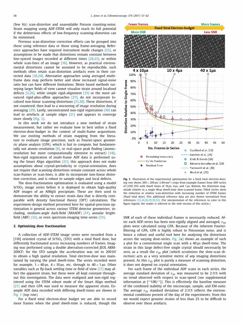
Fig. 1. Illustration of the experimental optimisation for a fixed total electron-dose;
top row shows 20 0 × 20 0 px (1.84 nm
2 ) crops from example frames from ADF-series
of [110] STO with dwell times of 10 μs, 4 μs, and 1 μs. Bottom, the distortion mag-
nitude relative to a single 40 μs dwell-time slow-scanned frame. Filled circles show
the reduction in relative scan-distortion with increasing number of STEM frames
(fixed total dose). Five additional reference data are also shown normalised from
references [15,24,26,29,30,32] . (For interpretation of the references to color in this
figure legend, the reader is referred to the web version of this article.)
S
t
p
fi
h
a
a
s
z
r
p
i
a
n
i
o
T
m
w
o
(few Hz) scan-distortion and unavoidable Poisson counting-noise.
Strain mapping using ADF-STEM will only reach its full potential
if the deleterious effects of low-frequency scanning-distortion can
be minimised.
Previous scan-distortion correction efforts can be grouped into
those using reference data or those using frame-averaging. Refer-
ence approaches have required instrument mode changes [23] , or
assumptions to be made that distortions remain constant between
line-synced images recorded at different times [24,25] , or within
whole scan-lines of an image [16] . However, as practical environ-
mental distortions cannot be assumed to be reproducible, such
methods often retain scan-distortion artefacts even in their cor-
rected data [16,24] . Alternative approaches using averaged multi-
frame data may perform better and show increased signal-noise
ratio but can have different limitations. Moire based methods sur-
veying larger fields of view cannot visualise strain around localised
defects [2,26] , while simple rigid-alignment [15] or the more ad-
vanced rigid-plus-affine approaches [27] , do not incorporate lo-
calised non-linear scanning-distortions [21,28] . These distortions, if
not countered, then lead to a worsening of image resolution during
averaging [29] . Lastly, unconstrained non-rigid registration [30] can
lead to artefacts at sample edges [21] and appears to converge
more slowly ( Fig. 1 ).
In this work we do not introduce a new method of strain
measurement, but rather we evaluate how to best utilise a fixed
electron-dose-budget in the context of multi-frame acquisitions.
We use existing methods of strain mapping from the litera-
ture to evaluate image precision, such as Fourier-space geomet-
ric phase analysis (GPA), which is fast to compute, but fundamen-
tally not atomic-resolution [8] , or real-space peak finding (atomic-
resolution but more computationally intensive to extract) [14] ;.
Non-rigid registration of multi-frame ADF data is performed us-
ing the Smart Align algorithm [21] ; this approach does not make
assumptions about crystal-periodicity or crystal-orientation, does
not require that scanning-distortions remain constant across whole
scan-frames or scan-lines, is able to incorporate non-linear distor-
tion correction, and is robust to sample edges and local defects.
The dose-fractionation optimisation is evaluated using a model
SrTiO 3 image series before it is deployed to obtain high-quality
ADF images of an AlMgSi precipitate. These are then used to
demonstrate the ability to extract strain data that is directly com-
parable with density functional theory (DFT) calculations. The
experiment-design method presented here for spatial-precision op-
timisation is general across various STEM detector geometries; in-
cluding, medium-angle dark-field (MAADF) [31] , annular bright-
field (ABF) [32] , or even spectrum-imaging time-series [33] .
2. Optimising dose fractionation
A collection of ADF-STEM image series were recorded from a
[110] oriented crystal of SrTiO 3 (STO) with a total fixed dose, but
differently fractionated across increasing numbers of frames. Imag-
ing was performed using a double aberration-corrected JEOL ARM-
200CF; for the STO sample the acceleration was set to 200 kV
to obtain a high spatial resolution. Total electron-dose was main-
tained by varying the pixel dwell-time. The series recorded were
for example, 1 × 40 μs, 4 × 10 μs, etc. through to 40 × 1 μs. Other
variables such as fly-back settling time or field of view [17] may af-
fect the apparent strain, but these were all kept constant through-
out this investigation. The data were realigned and non-rigid reg-
istered using the STEM robust mode of the Smart Align method
[21] and then GPA was used to measure the apparent strain. Ex-
ample ADF data recorded with differing dwell-times are shown in
Fig. 1 (top row).
For a fixed total electron-dose budget we are able to record
more frames when the pixel dwell-time is reduced, though the
NR of each of these individual frames is necessarily reduced. Af-
er each ADF-series has been non-rigidly aligned and averaged, εyy
lots were calculated using GPA. Because of the inherent Fourier-
ltering of GPA, GPA is highly robust to Poissonian noise, and is
ence a robust and useful tool here for analysing the distortions
cross the varying dose-series. Fig. 2 a) shows an example of such
plot for a conventional single scan with a 40 μs dwell-time. The
train in this large defect-free single crystal should necessarily be
ero, as a result the εyy plot (which scrutinises the slow-scan di-
ection) acts as a very sensitive metric of any imaging distortions
resent. As this εyy plot is purely a measure of scanning distortion,
t does not depend on crystal orientation.
For each frame of the individual ADF scans in each series, the
verage standard deviation of εyy was measured to be 2.11% with
o trend observed with respect to scan-speed (see supplemental
nformation at [ ∗∗URL ∗∗]). This is effectively the baseline measure
f the combined stability of the microscope, sample, and EM-suite.
he average εyy standard deviation of 2.11% reflects the environ-
ental conditions present of the day of the experiments; from this
e would expect genuine strains of less than 2% to be difficult to
bserve over these artefacts.

L. Jones et al. / Ultramicroscopy 179 (2017) 57–62 59
Fig. 2. Erroneous εyy strain plots caused by scan-distortion from, a) the single 40 μs scan and b) the non-rigid realigned restoration of 20 × 2 μs scans (same total dose). After
processing, the dose sharing multi-frame approach shows significant improvement in accuracy. FFT shows the spots selected for GPA. (For interpretation of the references to
color in this figure legend, the reader is referred to the web version of this article.)
t
w
a
s
T
d
f
f
t
g
f
d
l
t
t
a
w
s
a
T
l
c
e
w
d
n
o
t
t
s
u
t
w
f
t
t
d
a
c
e
t
t
w
f
c
p
f
i
c
t
e
o
n
(
c
p
s
t
2
o
t
f
3
m
o
f
a
3
r
s
[
m
t
n
f
a
v
i
m
n
b
i
s
a
o
[
r
F
(
Next, each of the image series were non-rigid registered using
he Smart Align algorithm [21] , averaged, and analysed in the same
ay. Fig. 2 b) shows an example εyy plot after scan correction and
veraging. To evaluate the improvement in strain-mapping preci-
ion, the ‘distortion relative to a single-frame’ is plotted in Fig. 1 .
his is defined as the standard deviation in εyy of the corrected
ata, divided by the standard deviation of εyy from the single-
rame. We find that, when moving to a dose-fractionated multi-
rame regime, the scan-correction and averaging approach reduced
he εyy standard deviation for all dose fractionation cases investi-
ated here, Fig. 1 (filled circles).
We can also consider what we expect to be the ultimate per-
ormance limit for this approach; if strain mapping in ADF is pre-
ominantly concerned with the reliable observation of Gaussian-
ike atomic columns, the precision of their position estimation is
hen the fundamental limit. For multi-frame data, the precision in
he position-estimation of the sum of Guassians shifted randomly
bout some true centre, would be expected to improve inversely
ith the square root of the number of observations, that is a clas-
ic 1/ �n behaviour, where n is the number of frames in the aver-
ge. This 1/ �n prediction is indicated in Fig. 1 (solid green line).
he difference between the obtained improvement and the 1/ �n
imit scales approximately linearly with the number of frames (in-
reasing dose fractionation) and adding together the 1/ �n and lin-
ar terms, we find a model which describes our experimental data
ell. One explanation for this extra linear term, may be that our
ata with the very lowest electron dose per frame perhaps can-
ot be completely re-registered, or that at such low dose some
ther source of read-out noise (perhaps from the amplification sys-
em) begins to limit the data quality. Previous studies have found
hat dwell-times faster than 2μs begin to show noticeable fast-
can streaking, while below 0.5μs these images become largely
nusable [34] . More recently this has been explained in terms of
he scintillator afterglow time constant [35,36] . This is consistent
ith the lack of improvement seen here between 20 and 40 times
ractionation of our constant total dose. For this reason the au-
hors here recommend that, using the current generation of de-
ectors/photomultipliers, 1.5μs should be considered as a minimum
well-time for ADF imaging.
Using the metric of ‘distortion relative to a single frame’, also
llows us to compare our new results with previous distortion-
orrection approaches from the literature; the normalisation of
ach literature data is described in the supplementary informa-
ion. The reduction in image distortion achieved here is consis-
ent with simple averaging and Moire approaches [15,26,29] , but
ith the advantage that it can be used for aperiodic features (de-
ects) and does not lose spatial resolution on averaging as is the
ase if non-linear distortions go uncorrected. Compared with ap-
roaches using line-synced reference images [24,25] , the approach
wollowed here delivered a better performance when eight or more
mages are used for the distortion correction. Furthermore, the
onditions are more flexible here as there is no need for the data
o be line-synced and no second sample is needed for the refer-
nce. Lastly, compared with isotropic non-rigid registration meth-
ds [30] , our STEM-bespoke scan-constrained method requires sig-
ificantly fewer frames to yield a similar relative improvement
e.g. ∼4 frames versus ∼100 frames for a 50% improvement). As
orrection of scan-noise (artefacts within scan-lines) does not im-
rove strain mapping precision (dependant on artefacts across
can-lines), these methods do not appear on Fig. 1 [20,22] .
Our optimisation approach then suggests that, for the condi-
ions used here, the total electron-dose should be shared across
0–30 frames yielding a distortion reduction to below 30% of the
riginal. With the environmental distortions present on the day of
he experiment, this is equivalent to an εyy precision improvement
rom ± 2.11% to ± 0.6%. For dose-fractionations across more than
0 frames, no significant further improvement was observed. Users
ay need to determine the optimum dose-fractionation for their
wn samples, instrument, or chosen total dose, but the approach
ollowed here is general. This approach then yielded the optimised
cquisition conditions for the next phase of experiments.
. Application to alloy precipitate strain measurement
Once acquisition parameters were optimised, ADF imaging was
epeated on a [100] oriented aluminium crystal containing needle-
haped β ’’ type AlMgSi precipitates imaged along their long axis
6,37] . Samples were prepared by electro-polishing following the
ethod in [38] from a material annealed at 195 °C for 4 hours af-
er homogenisation. EELS t/ λ measurements allow for the thick-
ess to be evaluated, and the highest-quality images were obtained
rom the thinnest regions of the foil where specimen thickness was
pproximately 20–40 nm. For the Al-alloy imaging the accelerating
oltage was set to 80 kV to avoid knock-on damage to the precip-
tates. For more details on microscope parameters, see the supple-
entary material. A precipitate running through the whole thick-
ess of the foil was selected that was far from any others and can
e treated as being alone in the Al matrix. Owing to the very high
n-plane strain there may be some corresponding relaxation in the
urface normal direction. Specimen relaxation could therefore give
small underestimate of the in-plane strain in the experimental
bservations. Further details may be found in previous publications
39,40] . 38 frames (2048 × 2048 pix) with 1.6 μs dwell time were
ecorded before alignment using the Smart Align algorithm [21] .
ig. 3 a) shows the central region from an average ADF-STEM frame
wider view in supplemental information).
The ADF image in Fig. 3 a) yields easily interpretable contrast,
ith both the structural unit and the edge of the precipitate read-

60 L. Jones et al. / Ultramicroscopy 179 (2017) 57–62
Fig. 3. a) Average ADF image restored by the smart align algorithm. The field of view is about 1/8 of the scan area (the whole field is shown in the supplement). b) εxx plot
measured using GPA with a 0.6 nm mask, and c) by real-space peak position measurement (same colour scale as b)). d) Atomic displacements (relative to a perfect lattice)
from the upper right part of the image. The arrows show the direction of the displacement, and are scaled larger by 3.1x with respect to magnitude which varies in the
range 0–0.08 nm. (For interpretation of the references to color in this figure legend, the reader is referred to the web version of this article.)
D
∼
t
t
a
o
y
i
i
t
t
s
e
c
f
G
g
s
f
s
A
f
t
a
m
f
a
I
ily identified; this is in contrast with HRTEM (see supplementary
information) where image contrast can be difficult to interpret.
Moreover, while not performed here, STEM also allows for simul-
taneous chemical analysis at atomic resolution [33] .
Precipitate strain fields were analysed by GPA and real-space
peak-position approaches ( Fig. 3 ) and compared with predictions
from DFT, Fig. 4 . For the real-space analysis these strains are the
differential displacements divided by the inter-column spacing. As
DFT computation scales with model size cubed, a 12 × 12 × 1 unit
supercell (576 atoms) was used. Four β ’ ’ formula units were in-
troduced by substituting Al according to established composition
and orientation relationships [41,42] . The precipitates were thus fi-
nite (but periodic) in the cross-sectional plane and infinite along
the needle direction ([001] Al ), Fig. 4 .
The strain analyses show that the aluminium columns are dis-
placed away from the precipitate by up to 0.08 nm in a radial
fashion, which is appropriate for such a needle-shaped precipitate
with a positive misfit with the lattice [43] . These plots highlight
however some differences between real- and reciprocal-space ap-
proaches; for GPA, the intrinsic limits of the mask used yield some
periodic artefacts along the precipitate edge, while the real-space
analysis, though at a better spatial resolution, exhibits more noise.
Because of this noise a least-squares fit to the strain field around
an cylindrical Eshelby inclusion is shown, yielding a scaling fac-
tor k = 0.864 nm
3 [43] . This real-space trend-line very closely re-
produces the DFT predicted misfit at the first Al-matrix atomic-
column (DFT = −3.633%, fit = −3.467%); this difference of 0.166%
corresponds to a discrepancy of 0.34 pm. After this first aluminium
lattice position, the observed strain decays faster for the smaller
FT simulation, reaching zero after approximately 1.5 nm, versus
6 nm for the experiment (see supplement). This is because of
he finite supercell size of the atomistic model – the superposi-
ion of periodic images of the precipitate more or less cancels out
t the supercell boundaries. Owing the computational limitations
f DFT it was not possible to increase the size of the supercell be-
ond 576 atoms at this time without compromising accuracy, but
n the future it may be possible to simulate larger cells. While
t is not the focus of this work to compare strain measurement
echniques, Fig. 4 also shows the overall reasonable agreement be-
ween GPA and real-space analyses of the same image. However it
hould be noted that GPA, containing only one Fourier spot within
ach mask, can never achieve atomic resolution and so appears
onsiderably smoothed relative to the real-space analysis. This ef-
ect is especially noticeable at the particle-matrix interface where
PA appreciably underestimates the strain predicted by DFT (GPA
ives around 2% compared with around 3.5% for the DFT & real-
pace analysis).
Lastly, if we take a region in the aluminium matrix from Fig. 3 b)
ar from the precipitate and analyse the strain-measurement preci-
ion, the standard deviation from non-rigid registered multi-frame
DF images was found to be 0.3%; this is better than the results
rom the STO owing to the better instrument stability on the day of
he experiment. For comparison, an HRTEM image was taken with
pixel-size and field-of-view similar to the ADF data (see supple-
entary information). The GPA precision from the Al-matrix was
ound to be 0.9%. This improved to 0.5% for an image recorded with
higher magnification, though this yielded a smaller field of view.
n contrast to scanned microscopies, as no scanning-distortions are

L. Jones et al. / Ultramicroscopy 179 (2017) 57–62 61
Fig. 4. a) Schematic of the model used for the DFT relaxation, b) the resulting εxx plot, and c) comparison of strain profiles outside a precipitate corner from STEM-GPA
(solid line), STEM peak-positions (open circles), DFT (solid squares), and HRTEM GPA (dashed line).
o
a
a
n
o
i
f
o
p
a
p
4
n
t
a
t
s
p
fi
m
T
H
f
e
i
s
e
t
A
a
t
P
a
t
A
t
bserved in HRTEM, GPA analysis does not benefit from frame-
veraging in the same way. In the literature HRTEM-GPA precisions
s good as 0.3% have been reported [9] , a precision which we are
ow able to match with ADF-STEM. This, combined with the ease
f interpretation of incoherent (z-contrast) ADF, and the ability to
nclude atomic resolution chemical mapping [44,45] , makes multi-
rame STEM a key new approach for mapping strain at atomic res-
lution.
Finally, whilst the multi-frame image alignment and averaging
recision improvement is impressive, it should be noted that it is
lways better to address environmental distortions at source before
ost-processing.
. Conclusions
Recent developments in non-rigid registration have spawned
ew questions in experiment design. Here fractionation of a fixed
otal electron-dose was studied with specific attention paid to the
ccuracy and precision of ADF-STEM strain data. After optimising
he experiment design, scanning artefacts were reduced by 70% for
eries with 20–30 frames.
To test the approach, experimental data were collected from β”
recipitates in aluminium. Their experimentally measured strain
elds were compared with DFT and found to be in good agree-
ent at the precipitate interface within an accuracy of around 1%.
he precision of multi-frame ADF-STEM was found to equal that of
RTEM-GPA for the first time, this combined with the opportunity
or simultaneous atomic-resolution spectroscopy opens exciting av-
nues in alloy microstructure characterisation by STEM.
Further work in calculating the interaction between dislocations
n Al and the strain field originating from precipitates of different
izes and atomic structure is underway [31] . This will help to refine
xisting models of precipitation strengthening for both fundamen-
al and industrial research.
uthor contributions statement
LJ designed the optimisation methodology and produced Figs. 1
nd 2 ; SW recorded the experimental data in Fig. 3 and performed
he alloy strain analyses; MN recorded the STO experimental data;
HN and OML configured and executed the DFT calculations; RH
nd PDN directed the research programme. All authors contributed
o writing and proofing the manuscript.
cknowledgments
The research leading to these results has received funding from
he European Union Seventh Framework Programme under Grant

62 L. Jones et al. / Ultramicroscopy 179 (2017) 57–62
[
Agreement 312483 - ESTEEM2 (Integrated Infrastructure Initiative–
I3) and from the Research Council of Norway (RCN) under the
FRINATEK project 221714/F20 . The TEM work was carried out on
the NORTEM instrument JEOL ARM-200CF at the TEM Gemini Cen-
tre at NTNU and SINTEF in Trondheim, Norway. Computational re-
sources were provided by the Notur consortium. The authors ac-
knowledge Eva Mørtsell for providing the Al alloy specimen.
Supplementary materials
Supplementary material associated with this article can be
found, in the online version, at doi:10.1016/j.ultramic.2017.04.007 .
References
[1] F. Guffarth, R. Heitz, A. Schliwa, O. Stier, N.N. Ledentsov, A.R. Kovsh, et al.,Strain engineering of self-organized InAs quantum dots, Phys. Rev. B. 64 (2001)
85305, doi: 10.1103/PhysRevB.64.085305 . [2] S. Kim, Y. Kondo, K. Lee, G. Byun, J. Jung Kim, S. Lee, et al., Quantitative
measurement of strain field in strained-channel-transistor arrays by scan-
ning moire´fringe imaging, Appl. Phys. Lett. 103 (2013) 33523, doi: 10.1063/1.4816286 .
[3] P. Gao, C.T. Nelson, J.R. Jokisaari, S.-H. Baek, C.W. Bark, Y. Zhang, et al., Reveal-ing the role of defects in ferroelectric switching with atomic resolution, Nat.
Commun. 2 (2011) 591, doi: 10.1038/ncomms1600 . [4] G. Catalan, A. Lubk, A.H.G. Vlooswijk, E. Snoeck, C. Magen, A. Janssens, et al.,
Flexoelectric rotation of polarization in ferroelectric thin films, Nat. Mater. 10(2011) 963–967, doi: 10.1038/nmat3141 .
[5] a. Llordés, A. Palau, J. Gázquez, M. Coll, R. Vlad, A. Pomar, et al., Nanoscale
strain-induced pair suppression as a vortex-pinning mechanism in high-temperature superconductors, Nat. Mater. 11 (2012) 329–336, doi: 10.1038/
nmat3247 . [6] E.A. Mørtsell, C.D. Marioara, S.J. Andersen, J. Røyset, O. Reiso, R. Holmestad,
Effects of Germanium, Copper, and Silver substitutions on hardness and mi-crostructure in lean Al-Mg-Si alloys, Metall. Mater. Trans. A. 46 (2015) 4369–
4379, doi: 10.1007/s11661-015-3039-5 .
[7] H. Seitz, M. Seibt, F.H. Baumann, K. Ahlborn, W. Schröter, Quantitative strainmapping using high-resolution electron microscopy, Phys. Status Solidi. 150
(1995) 625–634, doi: 10.1002/pssa.2211500206 . [8] M.J. Hÿtch, E. Snoeck, R. Kilaas, Quantitative measurement of displacement
and strain fields from HREM micrographs, Ultramicroscopy 74 (1998) 131–146,doi: 10.1016/S0304-3991(98)0 0 035-7 .
[9] F. Hüe, M.J. Hÿtch, H. Bender, F. Houdellier, A. Claverie, Direct mapping of
strain in a strained Silicon transistor by high-resolution electron microscopy,Phys. Rev. Lett. 100 (2008) 156602, doi: 10.1103/PhysRevLett.100.156602 .
[10] P. Zhang, A .A . Istratov, E.R. Weber, C. Kisielowski, H. He, C. Nelson, et al., Directstrain measurement in a 65 nm node strained silicon transistor by convergent-
beam electron diffraction, Appl. Phys. Lett. 89 (2006) 20–23, doi: 10.1063/1.2362978 .
[11] V.B. Ozdol, C. Gammer, X.G. Jin, P. Ercius, C. Ophus, J. Ciston, et al., Strain map-
ping at nanometer resolution using advanced nano-beam electron diffraction,Appl. Phys. Lett. 106 (2015) 253107, doi: 10.1063/1.4922994 .
[12] J.-L.L. Rouviere, A. Béché, Y. Martin, T. Denneulin, D. Cooper, A. Be ́che ,́ et al.,Improved strain precision with high spatial resolution using nanobeam pre-
cession electron diffraction, Appl. Phys. Lett. 103 (2013) 241913, doi: 10.1063/1.4829154 .
[13] A. Béché, J.L.L. Rouvière, J.P.P. Barnes, D. Cooper, Dark field electron hologra-
phy for strain measurement, Ultramicroscopy 111 (2011) 227–238, doi: 10.1016/j.ultramic.2010.11.030 .
[14] P.L. Galindo, S. Kret, A.M. Sanchez, J.-Y. Laval, A. Yáñez, J. Pizarro, et al., Thepeak pairs algorithm for strain mapping from HRTEM images, Ultramicroscopy
107 (2007) 1186–1193, doi: 10.1016/j.ultramic.2007.01.019 . [15] M. Couillard, G. Radtke, G.A. Botton, Strain fields around dislocation arrays in a
�9 silicon bicrystal measured by scanning transmission electron microscopy,Philos. Mag. 93 (2013) 1250–1267, doi: 10.1080/14786435.2013.778428 .
[16] J.-M. Zuo, A.B. Shah, H. Kim, Y. Meng, W. Gao, J.-L. Rouviére, Lattice and strain
analysis of atomic resolution Z-contrast images based on template matching,Ultramicroscopy 136 (2014) 50–60, doi: 10.1016/j.ultramic.2013.07.018 .
[17] D. Cooper, T. Denneulin, N. Bernier, A. Béché, J.-L. Rouvière, Strain mapping ofsemiconductor specimens with nm-scale resolution in a transmission electron
microscope, Micron 80 (2016) 145–165, doi: 10.1016/j.micron.2015.09.001 . [18] M.J. Hÿtch, A.M. Minor, Observing and measuring strain in nanostructures and
devices with transmission electron microscopy, MRS Bull. 39 (2014) 138–146,
doi: 10.1557/mrs.2014.4 . [19] D.A. Muller, E.J. Kirkland, M.G. Thomas, J.L. Grazul, L. Fitting, M. Weyland,
Room design for high-performance electron microscopy, Ultramicroscopy 106(2006) 1033–1040, doi: 10.1016/j.ultramic.2006.04.017 .
[20] L. Jones, P.D. Nellist, Identifying and correcting scan noise and drift in the scan-ning transmission electron microscope, Microsc. Microanal. 19 (2013) 1050–
1060, doi: 10.1017/S1431927613001402 .
[21] L. Jones, H. Yang, T.J. Pennycook, M.S.J. Marshall, S. Van Aert, N.D. Brown-ing, et al., Smart Align—a new tool for robust non-rigid registration of scan-
ning microscope data, Adv. Struct. Chem. Imag. 1 (2015) 8, doi: 10.1186/s40679- 015- 0 0 08-4 .
[22] N. Braidy, Y. Le Bouar, S. Lazar, C. Ricolleau, Correcting scanning instabilitiesfrom images of periodic structures, Ultramicroscopy 118 (2012) 67–76. http:
//dx.doi.org/10.1016/j.ultramic.2012.04.001 . accessed August 13, 2012 . [23] A. Recnik, G. Möbus, S. Sturm, IMAGE-WARP: a real-space restoration method
for high-resolution STEM images using quantitative HRTEM analysis, Ultrami-
croscopy 103 (2005) 285–301, doi: 10.1016/j.ultramic.2005.01.003 . [24] A.M. Sanchez, P.L. Galindo, S. Kret, M. Falke, R. Beanland, P.J. Goodhew, An ap-
proach to the systematic distortion correction in aberration-corrected HAADFimages, J. Microsc. 221 (2006) 1–7, doi: 10.1111/j.1365-2818.2006.01533.x .
[25] A.M. Sanchez, P.L. Galindo, S. Kret, M. Falke, R. Beanland, P.J. Goodhew, Quanti-tative strain mapping applied to aberration-corrected HAADF images, Microsc.
Microanal. 12 (2006) 285–294, doi: 10.1017/S1431927606060363 .
[26] N. Endo, Y. Kondo, Accuracy of strain in strain maps improved by averag-ing multiple maps, Microsc. Microanal. 20 (2014) 1068–1069, doi: 10.1017/
S1431927614007065 . [27] X. Sang, J.M. LeBeau, Revolving scanning transmission electron microscopy:
correcting sample drift distortion without prior knowledge, Ultramicroscopy138C (2013) 28–35, doi: 10.1016/j.ultramic.2013.12.004 .
[28] C. Ophus, J. Ciston, C.T. Nelson, Correcting nonlinear drift distortion of scan-
ning probe and scanning transmission electron microscopies from image pairswith orthogonal scan directions, Ultramicroscopy 162 (2016) 1–9, doi: 10.1016/
j.ultramic.2015.12.002 . [29] G. Bárcena-Gonzálaz, M.P. Guerrero-Lebrero, E. Guerrero, D. Fernández-Reyes,
D. González, A. Mayoral, et al., Strain mapping accuracy improvement usingsuper-resolution techniques, J. Microsc. 0 (2015) 1–9, doi: 10.1111/jmi.12341 .
[30] A.B. Yankovich, B. Berkels, W. Dahmen, P. Binev, S.I. Sanchez, S.A. Bradley,
et al., Picometre-precision analysis of scanning transmission electron mi-croscopy images of platinum nanocatalysts, Nat. Commun. 5 (2014), doi: 10.
1038/ncomms5155 . [31] S. Wenner, R. Holmestad, Accurately measured precipitate–matrix misfit in an
Al–Mg–Si alloy by electron microscopy, Scr. Mater. 118 (2016) 5–8, doi: 10.1016/j.scriptamat.2016.02.031 .
[32] M. Nord, P.E. Vullum, I. MacLaren, T. Tybell, R. Holmestad, Atomap: a new
software tool for the automated analysis of atomic resolution images us-ing two-dimensional Gaussian fitting, Adv. Struct. Chem. Imag. 3 (2017) 9,
doi: 10.1186/s40679- 017- 0042- 5 . [33] S. Wenner, L. Jones, C.D. Marioara, R. Holmestad, Atomic-resolution chemi-
cal mapping of ordered precipitates in Al alloys using energy-dispersive X-rayspectroscopy, Micron (2017), doi: 10.1016/j.micron.2017.02.007 .
[34] J.P. Buban, Q. Ramasse, B. Gipson, N.D. Browning, H. Stahlberg, High-resolution
low-dose scanning transmission electron microscopy, J. Electron Microsc.(Tokyo). 59 (2010) 103–112, doi: 10.1093/jmicro/dfp052 .
[35] F.F. Krause, M. Schowalter, T. Grieb, K. Müller-Caspary, T. Mehrtens, A. Rose-nauer, Effects of instrument imperfections on quantitative scanning transmis-
sion electron microscopy, Ultramicroscopy 161 (2016) 146–160, doi: 10.1016/j.ultramic.2015.10.026 .
[36] X. Sang, J.M. LeBeau, Characterizing the response of a scintillator-based detec-tor to single electrons, Ultramicroscopy 161 (2016) 3–9, doi: 10.1016/j.ultramic.
2015.11.008 .
[37] H.W. Zandbergen, S.J. Andersen, J. Jansen, Structure determination of Mg5Si6particles in Al by dynamic electron diffraction studies, Science 277 (80) (1997)
1221–1225, doi: 10.1126/science.277.5330.1221 . [38] S. Wenner, C.D. Marioara, S.J. Andersen, R. Holmestad, Effect of room tempera-
ture storage time on precipitation in Al–Mg–Si(–Cu) alloys with different Mg/Siratios, Int. J. Mater. Res. 103 (2012) 948–954, doi: 10.3139/146.110795 .
[39] P.H. Ninive, O.M. Løvvik, A. Strandlie, Density functional study of the β ′′ phase
in Al-Mg-Si alloys, Metall. Mater. Trans. A. 45 (2014) 2916–2924, doi: 10.1007/s11661- 014- 2214- 4 .
[40] P.H. Ninive, A. Strandlie, S. Gulbrandsen-Dahl, W. Lefebvre, C.D. Marioara,S.J. Andersen, et al., Detailed atomistic insight into the β ′′ phase in Al-Mg-Si
alloys, Acta Mater. 69 (2014) 126–134, doi: 10.1016/j.actamat.2014.01.052 . [41] S.J. Andersen, H.W. Zandbergen, J. Jansen, C. Træholt, U. Tundal, O. Reiso, The
crystal structure of the β ′′ phase in Al–Mg–Si alloys, Acta Mater. 46 (1998)
3283–3298, doi: 10.1016/S1359- 6454(97)00493- X . [42] H.S. Hasting, A.G. Fro ̸ seth, S.J. Andersen, R. Vissers, J.C. Walmsley, C.D. Mar-
ioara, et al., Composition of β[sup ̋ ] precipitates in Al–Mg–Si alloys by atomprobe tomography and first principles calculations, J. Appl. Phys. 106 (2009)
123527, doi: 10.1063/1.3269714 . [43] J. Douin, P. Donnadieu, F. Houdellier, Elastic strain around needle-shaped par-
ticles embedded in Al matrix, Acta Mater. 58 (2010) 5782–5788, doi: 10.1016/j.
actamat.2010.06.053 . 44] S.J. Kang, Y.-W. Kim, M. Kim, J.-M. Zuo, Determination of interfacial atomic
structure, misfits and energetics of � phase in Al–Cu–Mg–Ag alloy, Acta Mater.81 (2014) 501–511, doi: 10.1016/j.actamat.2014.07.074 .
[45] S. Wenner, C.D. Marioara, Q.M. Ramasse, D.-M. Kepaptsoglou, F.S. Hage,R. Holmestad, Atomic-resolution electron energy loss studies of precipitates
in an Al–Mg–Si–Cu–Ag alloy, Scr. Mater. 74 (2014) 92–95, doi: 10.1016/j.
scriptamat.2013.11.007 .


![complementtenseincontrast: …folk.uio.no/atleg/gronnstechow_sot_2010.pdfcomplementtenseincontrast [3] distancetransmissionoftemporalfeaturesfollowingthesotparameter,i.e.,non-localbinding](https://img.dokumen.tips/doc/110x75/5e2f3e42916a442f946a6d23/complementtenseincontrast-folkuionoatleggronnstechowsot2010pdf-complementtenseincontrast.jpg)