Embed Size (px)
Citation preview
w.wang
Optical Sources
Wei-Chih WangDepartment of Power Mechanical Engineering
National Tsinghua University
1

Week 10• Course Website: http://courses.washington.edu/me557/optics• Reading Materials: - Week 10 reading materials are from:
http://courses.washington.edu/me557/readings/• HW #2 due next Week• Prism Design Project presentation Week 13• Discussing proposal ideas Week 12• Final Project proposal: Due Monday Week 14• Final Project Presentation on 6/11 (Monday) 1:20-4:10PM• Next Monday – classs cancelled but extra credit if attending the
NTHU Photonics weeks (5/4 or 5/7). Please write up a reflection paper on things you saw in the exhibit.
• Make up class next Thursday (1:10 – 2:20PM)?w.wang 2
Light source
- Broadband light source- Light emitting diode- Laser
w.wang 3

4
What is Light?All the fifty years of conscious brooding have brought me no closer to the answer to the question, “what are light quanta?” Of course today every rascal thinks he knows the answer, but he is deluding (fooling) himself.
- Albert Einstein, 1951
Early days, a light beam was thought to consist of particles. Later, the phenomena of interference and diffraction were demonstrated which could be explained only by assuming a wave model of light. Much later, it was shown that phenomena such as photoelectric effect and Compton effect could be explained on if we assume a particle model of light.
* The photoelectric effect is the observation that many metals emit electrons when light shines upon them. Electrons emitted in this manner can be called photoelectrons. The phenomenon is commonly studied in electronic physics, as well as in fields of chemistry, such as quantum chemistry or electrochemistry (Wikipedia).* *Compton scattering is the inelastic scattering of a photon by a charged particle, usually an electron. It results in a decrease in energy (increase in wavelength) of the photon (which may be an X ray or gamma ray photon), called the Compton effect. (Wikipedia)
* Ajoy Ghatak, Optics, Macgraw Hill, 2010
W. Wang
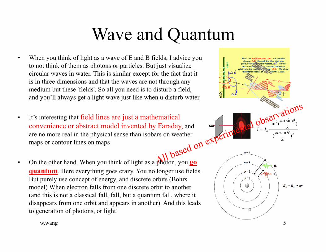
Wave and Quantum• When you think of light as a wave of E and B fields, I advice you
to not think of them as photons or particles. But just visualize circular waves in water. This is similar except for the fact that it is in three dimensions and that the waves are not through any medium but these 'fields'. So all you need is to disturb a field, and you’ll always get a light wave just like when u disturb water.
• It’s interesting that field lines are just a mathematical convenience or abstract model invented by Faraday, and are no more real in the physical sense than isobars on weather maps or contour lines on maps
• On the other hand. When you think of light as a photon, you go quantum. Here everything goes crazy. You no longer use fields. But purely use concept of energy, and discrete orbits (Bohrsmodel) When electron falls from one discrete orbit to another (and this is not a classical fall, fall, but a quantum fall, where it disappears from one orbit and appears in another). And this leads to generation of photons, or light!
w.wang 5
2
2
)sin(
)sin(sin
a
a
II o

Elements are completely pure.• All Matter is made up of Elements• They are only made of one type of ATOM
HELIUM ATOMw.wang 6

w.wang 7

Elements make up all living things.
O: OxygenC: CarbonH: HydrogenN: Nitrogen
w.wang 8

AtomSmallest particle of an element that still has the characteristics of that element
w.wang 9Planetary Model of Sodium Atom

Actual photograph of atoms of germanium in an ink-blot.
w.wang 10

Structure of an atom
• Proton (p+)• Neutron (n)
Electron cloudor Shell or LevelElectron (e-)
w.wang 11

Electron energy levels• Are regions where electrons travel
around the nucleus .• Each energy level can only hold a
certain number of electrons• 1st Shell = 2 electrons• 2nd Shell = 8 electrons• 3rd Shell = 8 electrons
w.wang 12
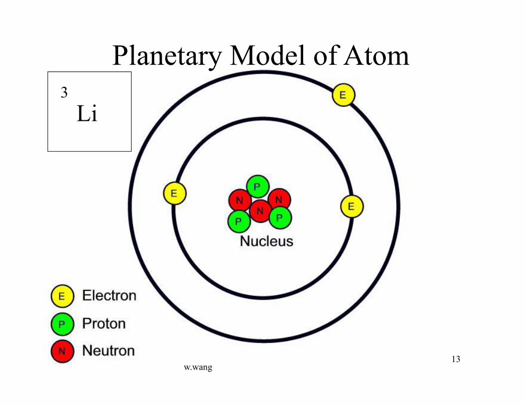
Li3
Planetary Model of Atom
w.wang13

Groups/Families• The elements in a column are called a group.• Groups are also known as families.• Elements in a group have similar characteristics.• The OUTER SHELL = VALENCE SHELL
w.wang 14

Periods• Each horizontal row is called a period.• A period contains a series of different type of
elements from different family.• They represent the # of SHELLS (shell #).
w.wang 15
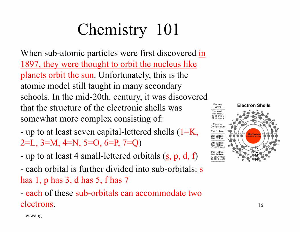
Chemistry 101When sub-atomic particles were first discovered in 1897, they were thought to orbit the nucleus like planets orbit the sun. Unfortunately, this is the atomic model still taught in many secondary schools. In the mid-20th. century, it was discovered that the structure of the electronic shells was somewhat more complex consisting of: - up to at least seven capital-lettered shells (1=K, 2=L, 3=M, 4=N, 5=O, 6=P, 7=Q) - up to at least 4 small-lettered orbitals (s, p, d, f) - each orbital is further divided into sub-orbitals: s has 1, p has 3, d has 5, f has 7 - each of these sub-orbitals can accommodate two electrons.
w.wang
16

w.wang 17
Helium
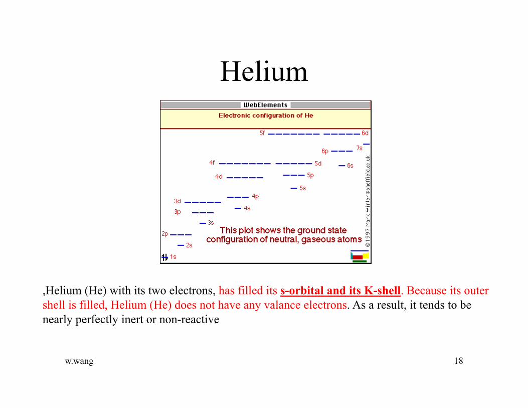
,Helium (He) with its two electrons, has filled its s-orbital and its K-shell. Because its outer shell is filled, Helium (He) does not have any valance electrons. As a result, it tends to be nearly perfectly inert or non-reactive
w.wang 18
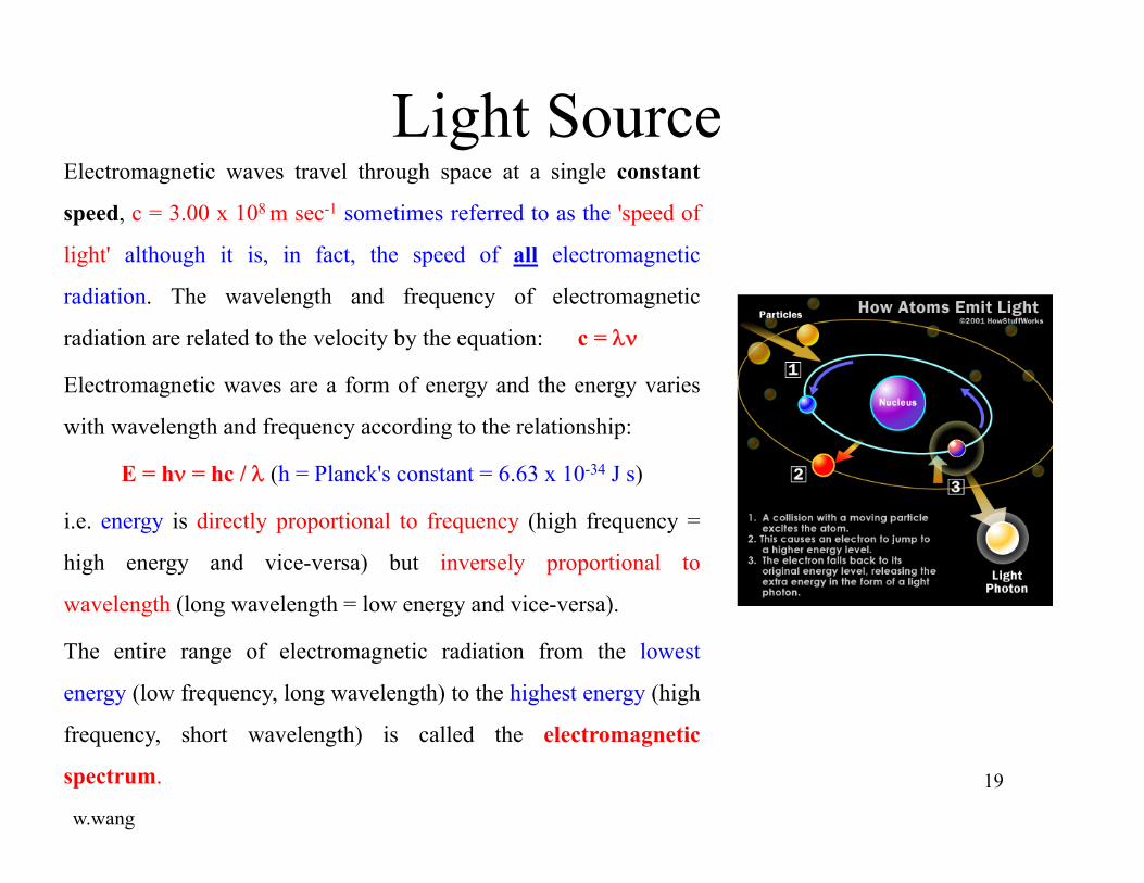
Light SourceElectromagnetic waves travel through space at a single constant
speed, c = 3.00 x 10⁸ m sec-1 sometimes referred to as the 'speed of
light' although it is, in fact, the speed of all electromagnetic
radiation. The wavelength and frequency of electromagnetic
radiation are related to the velocity by the equation: c =
Electromagnetic waves are a form of energy and the energy varies
with wavelength and frequency according to the relationship:
E = h = hc / (h = Planck's constant = 6.63 x 10⁻³⁴ J s)
i.e. energy is directly proportional to frequency (high frequency =
high energy and vice-versa) but inversely proportional to
wavelength (long wavelength = low energy and vice-versa).
The entire range of electromagnetic radiation from the lowest
energy (low frequency, long wavelength) to the highest energy (high
frequency, short wavelength) is called the electromagnetic
spectrum.
w.wang
19
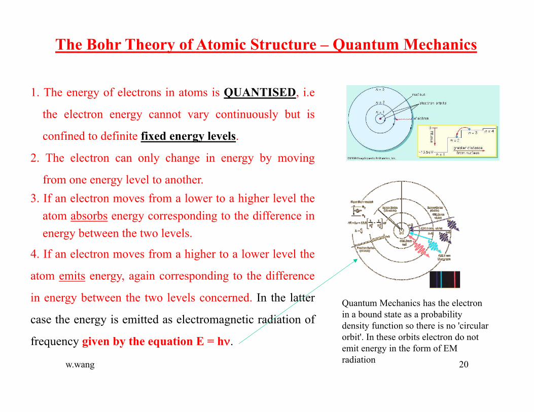
1. The energy of electrons in atoms is QUANTISED, i.e
the electron energy cannot vary continuously but is
confined to definite fixed energy levels.
2. The electron can only change in energy by moving
from one energy level to another.3. If an electron moves from a lower to a higher level the
atom absorbs energy corresponding to the difference inenergy between the two levels.
4. If an electron moves from a higher to a lower level the
atom emits energy, again corresponding to the difference
in energy between the two levels concerned. In the latter
case the energy is emitted as electromagnetic radiation of
frequency given by the equation E = h.
w.wang 20
The Bohr Theory of Atomic Structure – Quantum Mechanics
Quantum Mechanics has the electron in a bound state as a probability density function so there is no 'circular orbit'. In these orbits electron do not emit energy in the form of EM radiation

w.wang 21

w.wang 22

The Hydrogen Emission Spectrum
The hydrogen emission spectrum is a line spectrum, i.e. only particular frequencies (wavelengths, energies) are observed.
w.wang 23

The Hydrogen Emission Spectrum
The lines in the hydrogen emission spectrum are found to be grouped into line series: Lyman (Ultra Violet), Balmer (Visible), Brackett, Paschen and Pfund (all in the Infra Red region).
w.wang 24

WHAT IS GOING ON HERE?
Atom in 'excited state', i.e. with increased Energy (Hydrogen can be excited by heat or electromagnetic energy)
H2 2 H (energy)Molecule Atoms
H H*
w.wang 25

H* H + h
The excited atom returns to the 'normal' state (ground state) byreleasing the excess energy as electromagnetic radiation of energy(E= h) corresponding to the energy difference between theground state and the excited state.The fact that the hydrogen emission spectrum is a line spectrum –
only radiation of very specific frequencies being emitted – means
that only excited states of very specific energies are being formed.
w.wang 26

By inspection an empirical mathematical formula – the RydbergEquation - was found which predicted the position of all the lines in thespectrum:
When n1 = 1 and n2 = 2, 3, 4 …… ∞ the positions of the lines in theLyman (UV) series is predicted. The Balmer (visible) series is predictedby n1 = 2, n2 = 3, 4, 5 etc. The Brackett, Paschen and Pfund series (IR) arepredicted by n1 = 3, n1 = 4 and n1 = 5 respectively.
w.wang 27

Current• Electrons can be made to move from one
atom to another. When those electrons move between the atoms, a current of electricity is created. The electrons move from one atom to another in a "flow." One electron is attached and another electron is lost. It is a situation that's very similar to electricity passing along a wire and a circuit. The charge is passed from atom to atom when electricity is "passed." When electrons move among the atoms of matter, a current of electricity is created. This is what happens in a piece of wire. The electrons are passed from atom to atom, creating an electrical current from one end to other, just like in the picture. W. Wang 28

W. Wang 29
(current density, amp/m2)
x
y
zB = H = (1+) H = o(M+H)

W. Wang 30
use
Displacement current is electric field generated by B field that was radiating in air
Induced current is from dispersive medium like dielectric material
oror
c
1
D= E
tDJH

Electromagnetic Wave
W. Wang 31
id
is

w.wang
Light SourcesBroadband light sources: incoherent, intensity distribution no uniform across all spectrum (white light source)Hologen:250-1100nmKrpton:350-1700nmZenon (Xenon) :180- 2200nmDeuterium: 190-500nmMercury+Argon: 253.65 –1013.98nmDeuterium + halogen:190-900nmLED: range from 400 to 1800nmTungsten+ Hologen: 350-2000nm
Narrow band light source:Laser- 200 to 1800nm
32

Noble Gas
Noble Gases• Non-reactive• Full outer shell
w.wang 33

Broadband light source
w.wang 34

Broadband light source
• Incandescent filament Lamps• Gas Discharge light• LED
w.wang 35

Incandescent Filament LampsIn conventional filament lamps or light bulbs, electric current is passed through a coiled tungsten filament, contained in a glass envelope that is filled with an inert gas. When heated by an electrical current, the filament emits electromagnetic radiation. At lower temperatures, radiation is mainly emitted in the infrared part of the spectrum as heat. At higher temperatures, the proportion of radiation at wavelengths ranging from 380 to 780 nm increases and visible light is produced. In a conventional lamp, the filament temperatures are limited to about 2700 Kelvin. The tungsten filament starts to evaporate and as a result it leads to the blackening of the inside of the lamp envelope.
w.wang36
Tungsten filament lamp

Halogen
Halogen lamps are also filamentlamps. However, halogen is added to the fill gas to prevent evaporated tungsten from condensing on the inside of the lamp envelope. This feature is used to exploit higher filament temperatures of 3000K and beyond and allows the size of the lamp envelope to be significantly reduced
w.wang 37
tungsten halogen, quartz-halogen or quartz iodine lamp

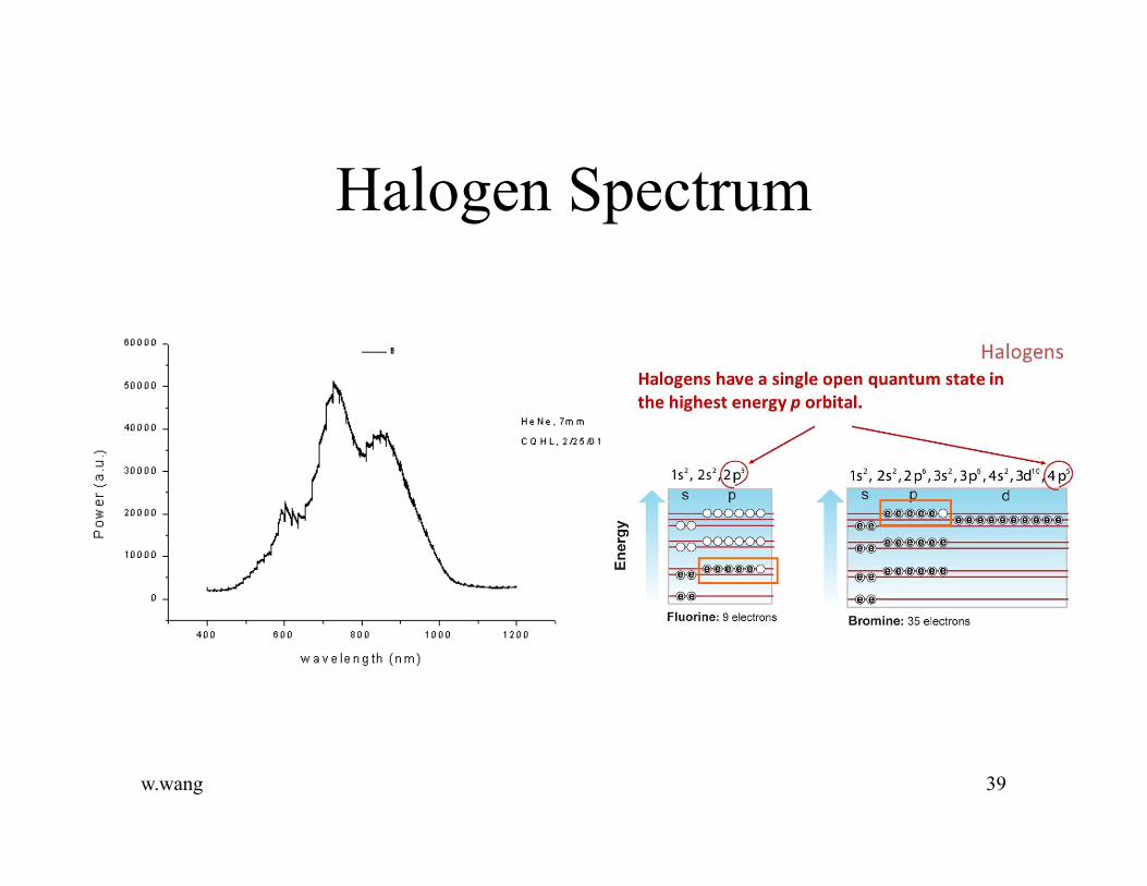
Halogen groupHalogens• Highly Reactive with alkali metals
•Missing 1 electron in outer shell
w.wang 38
w.wang
Halogen Spectrum
39

Tungsten Halogen Lamp
w.wang 40
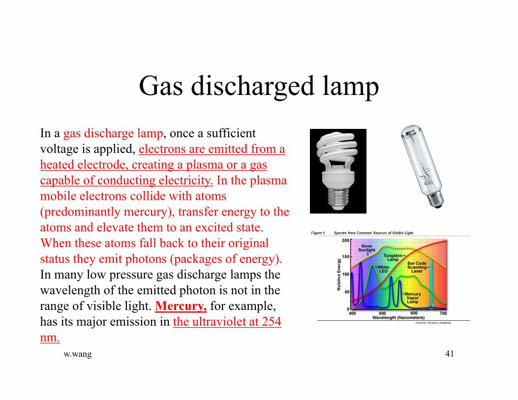
Gas discharged lampIn a gas discharge lamp, once a sufficient voltage is applied, electrons are emitted from a heated electrode, creating a plasma or a gas capable of conducting electricity. In the plasma mobile electrons collide with atoms (predominantly mercury), transfer energy to the atoms and elevate them to an excited state. When these atoms fall back to their original status they emit photons (packages of energy). In many low pressure gas discharge lamps the wavelength of the emitted photon is not in the range of visible light. Mercury, for example, has its major emission in the ultraviolet at 254 nm.
w.wang 41

Noble Gas
Noble Gases• Non-reactive• Full outer shell
w.wang 42

high intensity discharge lamp (e.g. metal halide lamp)
High pressure gas discharge lamps emit radiation directly as visible light. In this type of lamp the combination of different element atoms in the hot gas plasma, each emitting at specific wavelengths, determines the color characteristics of the lamp as a whole, as well as the quality of color rendition properties.
Most gas discharge lamps need at least one free electron combined with a high pulse to start the lamp operation and to produce light. Usually minute quantities of materials like tritium or krypton-85 are applied either in the lamps themselves or in starter devices as a source for electrons.
w.wang 43

Sodium Lamp
• Street light• horticulture
w.wang
Standard: North American / EuropeanLamp watts: 70-1000wBase type: E27, 40/MOGBulb shape: TD/ED/TD/ELUM. output: 6500-130000lmColor temp.: 2000kRated life: 18000-24000hr
44
The lamp is operating with liquid amalgam in the tube.

Mercury Lamp
• Gas charging lamp• 10 and 100 times brighter than
incandescent lamps (such as the tungsten-halogen) and can provide intense illumination over selected wavelength bands throughout the visible spectral region when combined with the appropriate filters (e.g.. Photolithography)
w.wang 45

low-pressure mercury gas discharge fluorescent lamp
Ultraviolet photons have the capability to excite fluorescent powders, which are coated on the inside of the tube, with a high degree of efficiency. As a result, these powders emit visible radiation in a range of colors. Lamps based on these principles and operating at low internal gas pressure are called “fluorescent lamps”.
w.wang 46
Phosphor coating

w.wang
47
Incandescent
•Regular•Halogen•Nernst•Parabolic aluminized reflector (PAR)
Luminescent
•Fluorescent• Fluorescent lamp (compact)• Fluorescent induction
•Photoluminescent• laser lamp
•Solid-state• LED bulb
•Cathodoluminescent• Electron-stimulated
•Electroluminescent• field-induced polymer
Methods of generation
Combustion
•Acetylene/Carbide•Argand•Candle•Diya•Flare•Gas•Kerosene•Lantern•Limelight•Oil•Rushlight•Safety•Tilley•Torch
Electric arc•Carbon arc•Klieg light•Yablochkov candle
Gas discharge
•Deuterium arc•Neon•Plasma•Sulfur•Xenon arc•Xenon flash
High-intensitydischarge (HID)
•Hydrargyrum medium-arc iodide (HMI)•Hydrargyrum quartz iodide (HQI)•Mercury-vapor•Metal-halide
• ceramic•Sodium vapor
wikipedia

w.wang 48
Application
•Theatrical•Cinematic
•Floodlight•Footlight•Gobo•Scoop•Spotlight•ellipsoidal reflector•Stage lighting instrument
Stationary
•Aircraft warning•Balanced-arm lamp•Chandelier•Emergency light•Gas lighting•Gooseneck lamp•Intelligent street lighting•Light tube•Nightlight•Neon lighting•Pendant light•Recessed light•Sconce•Street light•Torchère•Track lighting•Troffer
Mobile
•Flashlight•tactical•Glow stick•Headlamp (outdoor)•Lantern•Laser pointer•Navigation light•Searchlight•Solar lamp
•Industrial•Scientific
•Germicidal•Grow light•Infrared lamp•Stroboscope•Tanning
•Display•Decorative
•Aroma lamp•Black light•Bubble light•Christmas lights•Crackle tube•DJ lighting•Electroluminescent wire•Lava lamp•Marquee•Plasma globe•Strobe light
Related topics
•Bioluminescence•Chemiluminescence•Electroluminescence•Laser•Photoluminescence•Radioluminescence
wikipedia
w.wang 49
Ideas for final projects- using differentTypes of lights for “unseen” application

Light Emitting Diode
w.wang 50

Linear and Nonlinear electronics
Vaccum tube(i.e. type 2A3)
Thermistor
voltagevoltage voltage Diode
(i.e. PN diode, LED,laser diode, phtodiode)(large negative
temperaturecoefficient ofresistivity)
Normal resistor
voltage
current
currentOhm’s Law: i=v/R
1T
DnV
v
SD eIi
w.wang 51

Introduction to Diodes
• A diode can be considered to be an electrical one-way valve.
• They are made from a large variety of materials including silicon, germanium, gallium arsenide, silicon carbide …
ANODED1
DIODECATHODE
w.wang 52
-+
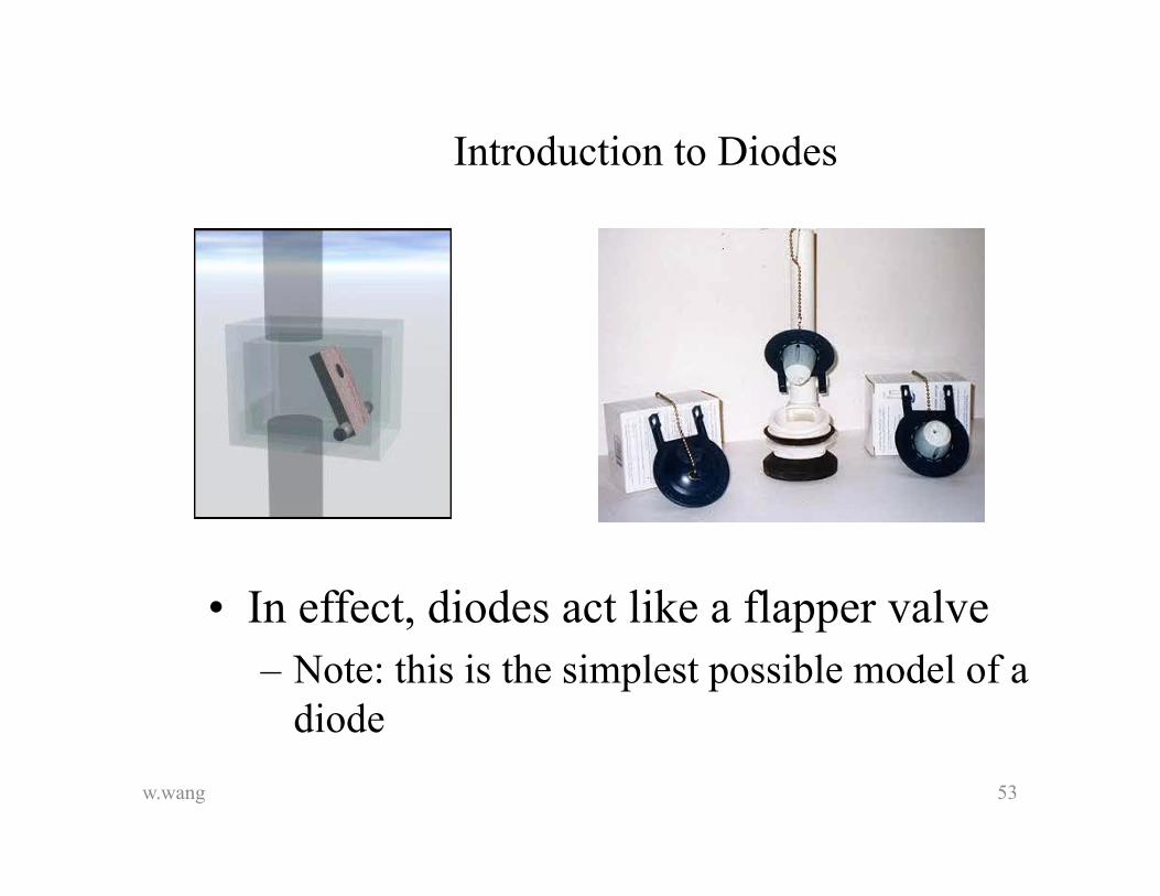
Introduction to Diodes
• In effect, diodes act like a flapper valve– Note: this is the simplest possible model of a
diodew.wang 53
Introduction to Diodes
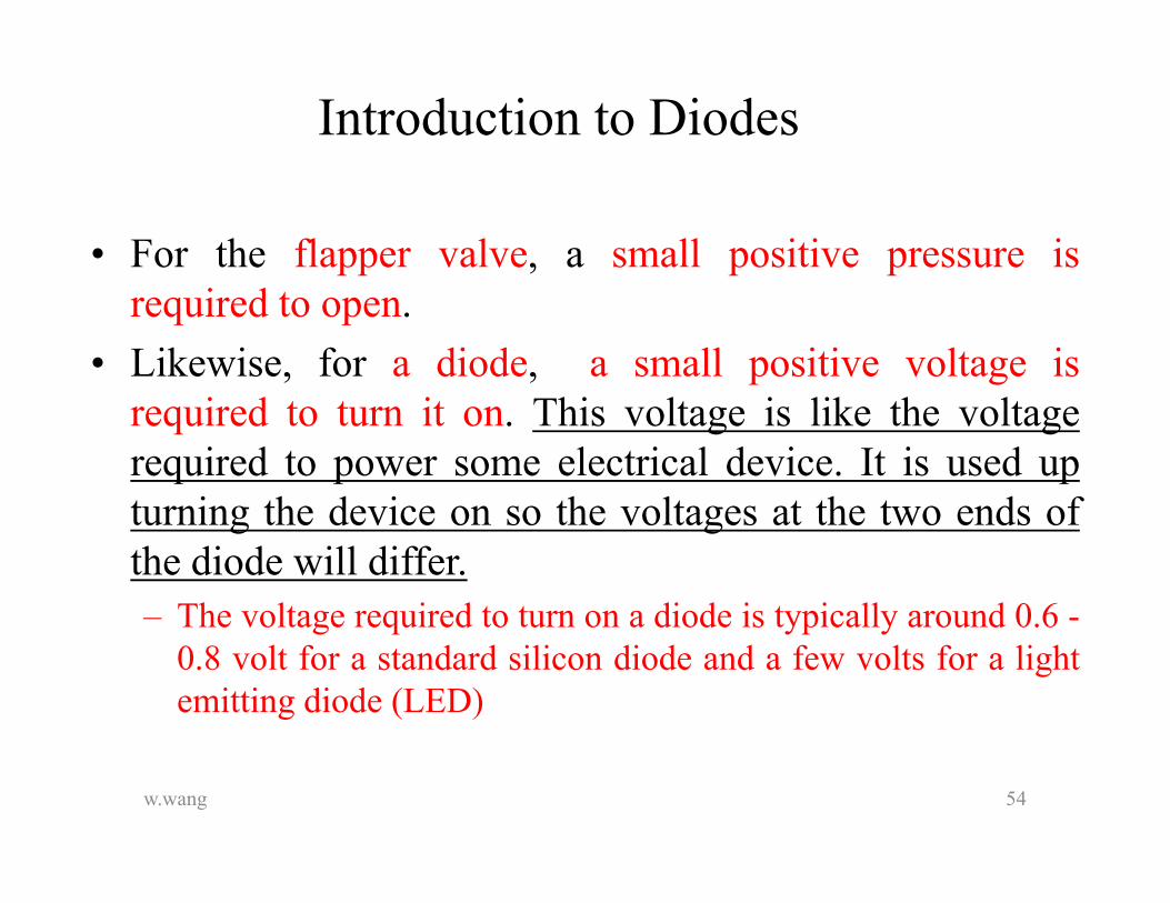
• For the flapper valve, a small positive pressure isrequired to open.
• Likewise, for a diode, a small positive voltage isrequired to turn it on. This voltage is like the voltagerequired to power some electrical device. It is used upturning the device on so the voltages at the two ends ofthe diode will differ.– The voltage required to turn on a diode is typically around 0.6 -
0.8 volt for a standard silicon diode and a few volts for a lightemitting diode (LED)
w.wang 54

• 10 volt sinusoidal voltage source
• Connect to a resistive load through a diode
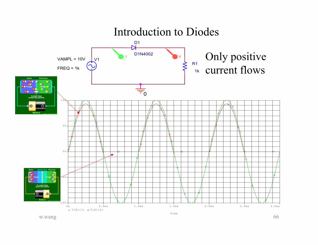
Introduction to Diodes
V1
FREQ = 1k
VAMPL = 10V
0
R1
1k
D1
D1N4002
T i m e
0 s 0 . 5 m s 1 . 0 m s 1 . 5 m s 2 . 0 m s 2 . 5 m s 3 . 0 m sV ( D 1 : 1 )
- 1 0 V
- 5 V
0 V
5 V
1 0 V
w.wang 55
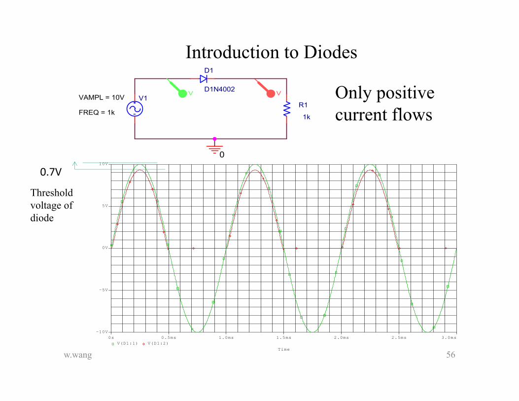
Introduction to Diodes
Only positivecurrent flows
0
VV
R1
1k
D1
D1N4002V1
FREQ = 1k
VAMPL = 10V
Time
0s 0.5ms 1.0ms 1.5ms 2.0ms 2.5ms 3.0msV(D1:1) V(D1:2)
-10V
-5V
0V
5V
10V
0.7V
Threshold voltage of diode
w.wang 56

SemiconductorVariable conductivity
A pure semiconductor is a poor electrical conductor as a consequence of having just the right number of electrons to completely fill its valence bonds. Through various techniques (e.g., doping or gating), the semiconductor can be modified to have excess of electrons (becoming an n-type semiconductor) or a deficiency of electrons (becoming a p-type semiconductor). In both cases, the semiconductor becomes much more conductive (the conductivity can be increased by a factor of one million, or even more). Semiconductor devices exploit this effect to shape electrical current.
JunctionsWhen doped semiconductors are joined to metals, to different semiconductors, and to the same semiconductor with different doping, the resulting junction often strips the electron excess or deficiency out from the semiconductor near the junction. This depletion region is rectifying (only allowing current to flow in one direction), and used to further shape electrical currents in semiconductor devices.
Energetic electrons travel farElectrons can be excited across the energy band gap of a semiconductor by various means. These electrons can carry their excess energy over distance scales of microns before dissipating their energy into heat, significantly longer than is possible in metals. This effect is essential to the operation of bipolar junction transistors.
Light energy conversionElectrons in a semiconductor can absorb light, and subsequently retain the energy from the light for a long enough time to be useful for producing electrical work instead of heat. This principle is used in the photovoltaic cell (e.g. solar cell).Conversely, in certain semiconductors, electrically excited electrons can relax by emitting light instead of producing heat. This is used in the light emitting diode.
Thermal energy conversionSemiconductors are good materials for thermoelectric coolers and thermoelectric generators, which convert temperature differences into electrical power and vice versa. Peltier coolers use semiconductors for this reason.
w.wang 57

SemiconductorVariable conductivity
A pure semiconductor is a poor electrical conductor as a consequence of having just the right number of electrons to completely fill its valence bonds. Through various techniques (e.g., doping or gating), the semiconductor can be modified to have excess of electrons (becoming an n-type semiconductor) or a deficiency of electrons (becoming a p-type semiconductor). In both cases, the semiconductor becomes much more conductive (the conductivity can be increased by a factor of one million, or even more). Semiconductor devices exploit this effect to shape electrical current.
JunctionsWhen doped semiconductors are joined to metals, to different semiconductors, and to the same semiconductor with different doping, the resulting junction often strips the electron excess or deficiency out from the semiconductor near the junction. This depletion region is rectifying (only allowing current to flow in one direction), and used to further shape electrical currents in semiconductor devices.
Energetic electrons travel farElectrons can be excited across the energy band gap of a semiconductor by various means. These electrons can carry their excess energy over distance scales of microns before dissipating their energy into heat, significantly longer than is possible in metals. This effect is essential to the operation of bipolar junction transistors.
Light energy conversionElectrons in a semiconductor can absorb light, and subsequently retain the energy from the light for a long enough time to be useful for producing electrical work instead of heat. This principle is used in the photovoltaic cell (e.g. solar cell).Conversely, in certain semiconductors, electrically excited electrons can relax by emitting light instead of producing heat. This is used in the light emitting diode.
Thermal energy conversionSemiconductors are good materials for thermoelectric coolers and thermoelectric generators, which convert temperature differences into electrical power and vice versa. Peltier coolers use semiconductors for this reason.
w.wang 58
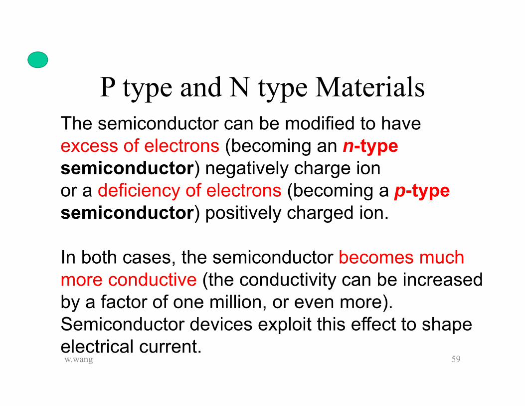
P type and N type MaterialsThe semiconductor can be modified to have excess of electrons (becoming an n-type semiconductor) negatively charge ion or a deficiency of electrons (becoming a p-typesemiconductor) positively charged ion.
In both cases, the semiconductor becomes much more conductive (the conductivity can be increased by a factor of one million, or even more). Semiconductor devices exploit this effect to shape electrical current.w.wang 59

Donor ( n type semiconductors)In semiconductor physics, a donor is a dopant atom that, when added to a semiconductor, can form a n-type region.For example, when silicon (Si), having four valence electrons, needs to be doped as an n-type semiconductor, elements from group V like phosphorus (P) or arsenic (As) can be used because they have five valence electrons. A dopant with five valence electrons is also called a pentavalent impurity. Other pentavalent dopants are antimony (Sb) and bismuth (Bi).
When substituting a Si atom in the crystal lattice, four of the valence electrons of phosphorus form covalent bonds with the neighbouring Si atoms but the fifth one remains weakly bonded. At room temperature, all the fifth electrons are liberated, can move around the Si crystal and can carry a current and thus act as charge carriers. The initially neutral donor becomes positively charged (ionised).
w.wang 60
Group V
Extra e-
diffusion
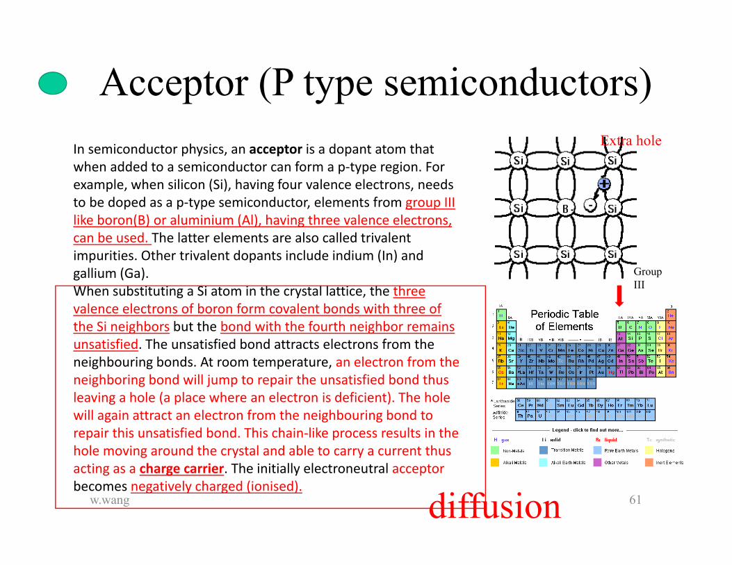
Acceptor (P type semiconductors)In semiconductor physics, an acceptor is a dopant atom that when added to a semiconductor can form a p‐type region. For example, when silicon (Si), having four valence electrons, needs to be doped as a p‐type semiconductor, elements from group III like boron(B) or aluminium (Al), having three valence electrons, can be used. The latter elements are also called trivalent impurities. Other trivalent dopants include indium (In) and gallium (Ga).When substituting a Si atom in the crystal lattice, the three valence electrons of boron form covalent bonds with three of the Si neighbors but the bond with the fourth neighbor remains unsatisfied. The unsatisfied bond attracts electrons from the neighbouring bonds. At room temperature, an electron from the neighboring bond will jump to repair the unsatisfied bond thus leaving a hole (a place where an electron is deficient). The hole will again attract an electron from the neighbouring bond to repair this unsatisfied bond. This chain‐like process results in the hole moving around the crystal and able to carry a current thus acting as a charge carrier. The initially electroneutral acceptor becomes negatively charged (ionised).
w.wang 61
Group III
Extra hole
diffusion

SemiconductorVariable conductivity
A pure semiconductor is a poor electrical conductor as a consequence of having just the right number of electrons to completely fill its valence bonds. Through various techniques (e.g., doping or gating), the semiconductor can be modified to have excess of electrons (becoming an n-type semiconductor) or a deficiency of electrons (becoming a p-type semiconductor). In both cases, the semiconductor becomes much more conductive (the conductivity can be increased by a factor of one million, or even more). Semiconductor devices exploit this effect to shape electrical current.
JunctionsWhen doped semiconductors are joined to metals, to different semiconductors, and to the same semiconductor with different doping, the resulting junction often strips the electron excess or deficiency out from the semiconductor near the junction. This depletion region is rectifying (only allowing current to flow in one direction), and used to further shape electrical currents in semiconductor devices.
Energetic electrons travel farElectrons can be excited across the energy band gap of a semiconductor by various means. These electrons can carry their excess energy over distance scales of microns before dissipating their energy into heat, significantly longer than is possible in metals. This effect is essential to the operation of bipolar junction transistors.
Light energy conversionElectrons in a semiconductor can absorb light, and subsequently retain the energy from the light for a long enough time to be useful for producing electrical work instead of heat. This principle is used in the photovoltaic cell (e.g. solar cell).Conversely, in certain semiconductors, electrically excited electrons can relax by emitting light instead of producing heat. This is used in the light emitting diode.
Thermal energy conversionSemiconductors are good materials for thermoelectric coolers and thermoelectric generators, which convert temperature differences into electrical power and vice versa. Peltier coolers use semiconductors for this reason.
w.wang 62
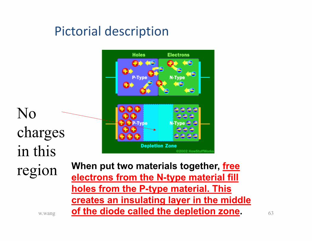
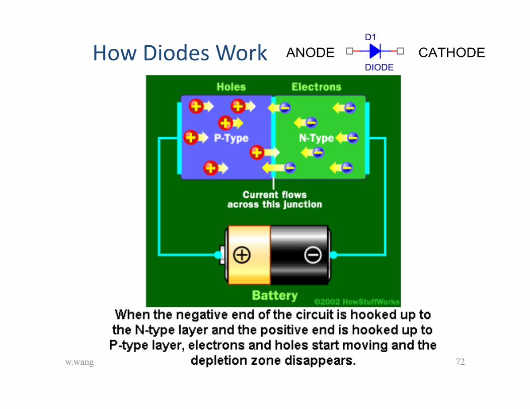
When put two materials together, free electrons from the N-type material fill holes from the P-type material. This creates an insulating layer in the middle of the diode called the depletion zone.
Pictorial description
w.wang 63
No charges in this region
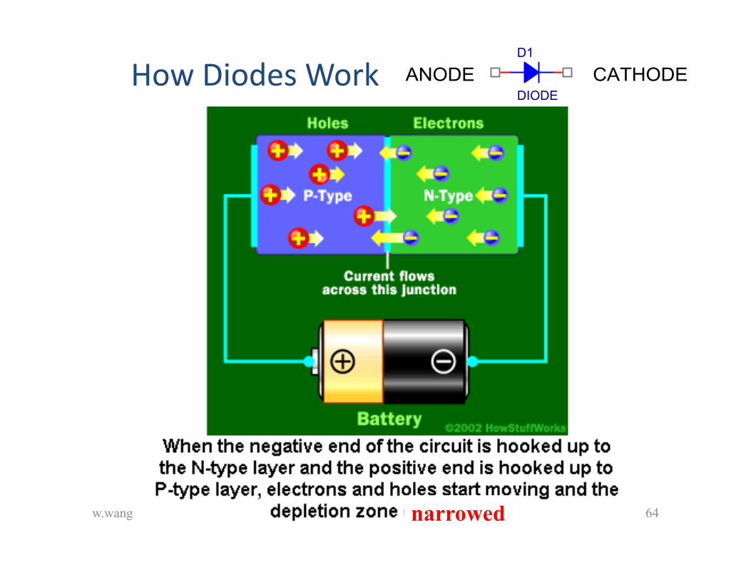
How Diodes Work ANODED1
DIODECATHODE
w.wang 64narrowed

How Diodes Work
When the positive end of the battery is hooked up to the N-type layer and the negative end is hooked up to the P-type layer, free electrons collect on one end of the diode and holes collect on the other. The depletion zone gets bigger and no current flows.
ANODED1
DIODECATHODE
w.wang 65
Introduction to Diodes
Only positivecurrent flows
0
VV
R1
1k
D1
D1N4002V1
FREQ = 1k
VAMPL = 10V
Time
0s 0.5ms 1.0ms 1.5ms 2.0ms 2.5ms 3.0msV(D1:1) V(D1:2)
-10V
-5V
0V
5V
10V
w.wang 66

Part A: Diode i-v Characteristic Curves
• What is a i‐v characteristic curve?
• i‐v curve of an ideal diode
• i‐v curve of a real diode
w.wang 67

What is an i-v characteristic curve?• Recall that the i-v relationship for a resistor
is given by Ohm’s Law: i=v/R• If we plot the voltage across the resistor vs.
the current through the resistor, we obtain
v
iThe slope of the straight line is given by 1/R
w.wang 68

What is an i-v characteristic curve?If we change the axis variables, we can obtain i-v characteristic curves.
0
V115V
R1
500
R2
1k
V(R1:1) - V(R1:2)
-6.0V -4.0V -2.0V 0V 2.0V 4.0V 6.0VI(R1)
-10mA
-5mA
0A
5mA
10mA
V-I Characteristic of a 500 Ohm Resistor
w.wang 69

i-v characteristic for an ideal diode
Ideal Diode
iD
vD0When voltage across the diode is positive, the diode looks like a short.
When voltage across the diode is negative, the diode looks like an open circuit.
w.wang 70
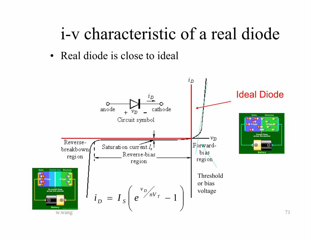
i-v characteristic of a real diode• Real diode is close to ideal
Ideal Diode
1T
DnV
v
SD eIiw.wang 71
Threshold or bias voltage
How Diodes Work ANODED1
DIODECATHODE
w.wang 72
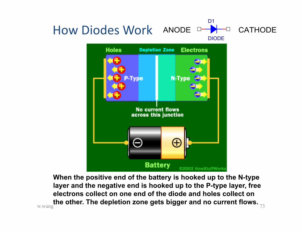
How Diodes Work
When the positive end of the battery is hooked up to the N-type layer and the negative end is hooked up to the P-type layer, free electrons collect on one end of the diode and holes collect on the other. The depletion zone gets bigger and no current flows.
ANODED1
DIODECATHODE
w.wang 73

Energy levels
Helium (He) with its two electrons, has filled its s‐orbital and its K‐shell. Because its outer shell is filled, Helium (He) does not have any valance electrons. As a result, it tends to be nearly perfectly inert or non‐reactive
w.wang 74

Forward Bias
h hc
w.wang 75
Whole bunch of interbands not shown

Real diode characteristics
• A very large current can flow when the diode is forward biased. For power diodes, currents of a few amps can flow with bias voltages of 0.6 to 1.5V. Note that the textbook generally uses 0.6V as the standard value, but 0.7V is more typical for the devices.
• Reverse breakdown voltages can be as low as 50V and as large as 1000V.
• Reverse saturation currents Is are typically 1nA or less.
w.wang 76

The diode equation• The iD-vD relationship (without breakdown) can be written
simply as:
• vD is the voltage across the diode and iD is the current through the diode. n and Is are constants. VT is a voltage proportional to the temperature, we use 0.0259V.
• Note that for vD less than zero, the exponential term vanishes and the current iD is roughly equal to minus the saturation current.
• For vD greater than zero, the current increases exponentially.
1T
DnV
v
SD eIi
w.wang 77

Diode equation
Both the simulated current vs. voltage (green) and the characteristic equation (red) for the diode are plotted.
-16V -14V -12V -10V -8V -6V -4V -2V 0V 2V
0
4m
8m
12m
16m
19m
iD
1T
DnV
v
SD eIi
V25V
R1
1k
D1D1N4148
0
0 exponential term takes over< 0 exponential terms << 1 so Is takes over
Using resistor R1 to control iDsince intrinsic resistance is small in thee diode / 1
w.wang 78

SemiconductorVariable conductivity
A pure semiconductor is a poor electrical conductor as a consequence of having just the right number of electrons to completely fill its valence bonds. Through various techniques (e.g., doping or gating), the semiconductor can be modified to have excess of electrons (becoming an n-type semiconductor) or a deficiency of electrons (becoming a p-type semiconductor). In both cases, the semiconductor becomes much more conductive (the conductivity can be increased by a factor of one million, or even more). Semiconductor devices exploit this effect to shape electrical current.
JunctionsWhen doped semiconductors are joined to metals, to different semiconductors, and to the same semiconductor with different doping, the resulting junction often strips the electron excess or deficiency out from the semiconductor near the junction. This depletion region is rectifying (only allowing current to flow in one direction), and used to further shape electrical currents in semiconductor devices.
Energetic electrons travel farElectrons can be excited across the energy band gap of a semiconductor by various means. These electrons can carry their excess energy over distance scales of microns before dissipating their energy into heat, significantly longer than is possible in metals. This effect is essential to the operation of bipolar junction transistors.
Light energy conversionElectrons in a semiconductor can absorb light, and subsequently retain the energy from the light for a long enough time to be useful for producing electrical work instead of heat. This principle is used in the photovoltaic cell (e.g. solar cell).Conversely, in certain semiconductors, electrically excited electrons can relax by emitting light instead of producing heat. This is used in the light emitting diode.
Thermal energy conversionSemiconductors are good materials for thermoelectric coolers and thermoelectric generators, which convert temperature differences into electrical power and vice versa. Peltier coolers use semiconductors for this reason.
w.wang 79

w.wang
Light Emitting Diode (LED)The electroluminescent process of LED is to covert input electrical energy into output optical radiation in the visible or infrared (heat) portion of the spectrum, depending on the semiconductor material.
LEDs and laser diodes are very similar devices. In fact, when operating below their threshold current, all laser diodes act as LEDs.
80

Light Emitting Diodes– The Light-Emitting Diode
(LED) is a semiconductor pn junction diode that emits visible light or near-infrared radiation when forward biased.
– Visible LEDs emit relatively narrow bands of green, yellow, orange, or red light (tens of nm). Infrared LEDs emit in one of several bands just beyond red light.
w.wang 81
+ -

Facts about LEDs– LEDs switch off and on rapidly, are very
rugged and efficient, have a very long lifetime, and are easy to use (~ns to s).
– They are current-dependent sources, and their light output intensity is directly proportional to the forward current through the LED.
– Always operate an LED within its ratings to prevent irreversible damage.
– Use a series resistor (Rs) to limit the current through the LED to a safe value. VLED is the LED voltage drop. It ranges from about 1.3V to about 3.6V. Intrinsic resistance of LED is small (~ 10ohms)
– ILED is the specified forward current. (Generally 20mA).
in LEDs
LED
V VRI
w.wang 82
~ cutoff frequency, capacitance value

Approximate LED threshold voltages
Diode VLED Diode VLED
infra-red 1.2 blue 3.6
red 2.2 purple 3.6
yellow 2.2 ultra-violet 3.7
green 3.5 white 3.6
w.wang 83
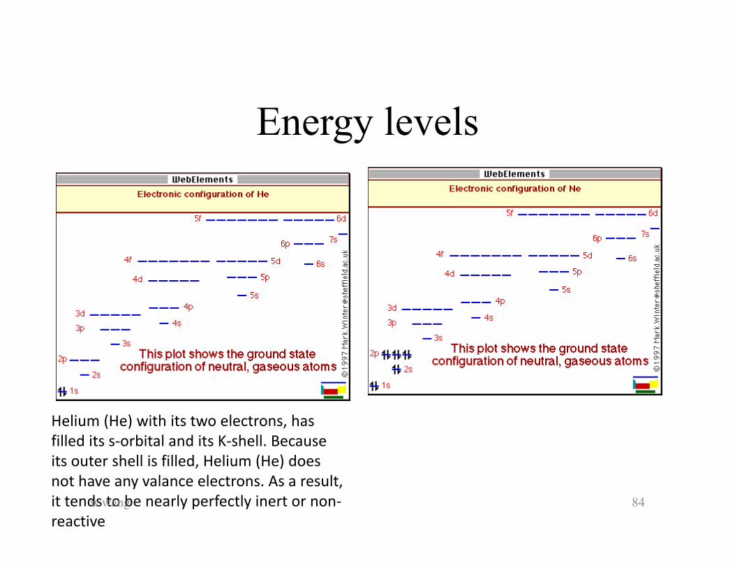
Energy levels
Helium (He) with its two electrons, has filled its s‐orbital and its K‐shell. Because its outer shell is filled, Helium (He) does not have any valance electrons. As a result, it tends to be nearly perfectly inert or non‐reactive
w.wang 84

Light SourceElectromagnetic waves travel through space at a single constant speed, c = 3.00 x 10⁸ m sec-1
sometimes referred to as the 'speed of light' although it is, in fact, the speed of all
electromagnetic radiation. The wavelength and frequency of electromagnetic radiation are
related to the velocity by the equation:
c =
Electromagnetic waves are a form of energy and the energy varies with wavelength and
frequency according to the relationship:
E = h = hc / (h = Planck's constant = 6.63 x 10⁻³⁴ J s)
i.e. energy is directly proportional to frequency (high frequency = high energy and vice-versa)
but inversely proportional to wavelength (long wavelength = low energy and vice-versa).
The entire range of electromagnetic radiation from the lowest energy (low frequency, long
wavelength) to the highest energy (high frequency, short wavelength) is called the
electromagnetic spectrum.w.wang 85

Forward Bias
h hc
w.wang 86

Forward and Reverse Bias
w.wang 87

The energy conversion takes place in two stages: first, the energy of carriers in the semiconductor is raised above their equilibrium value by electrical input energy, and second, most of these carriers, after having lived a mean lifetime in the higher energy state, give up their energy as spontaneous emission of photons with energy nearly equal to the bandgap Eg of the semiconductor:
Ego = h hc
where h is plank constant and is frequency of emitting light.
The choice of LED materials requires the wavelength light emission to be within visible light or infrared light region. This means that the bandgap of the semiconductor has to be roughly around 2 eV. The most frequency used binary compounds for LED applications are III-V compounds such as GaAs and GaP. In your case, the red diode could be made of a homojunction GaAsP (650nm) diode and the yellow diode made of a homojunction GaAsP:N (585nm) diode, where N representing doping level.
w.wang 88

The typical spectral output of a LED might looks like:
Spectra of different color LEDs
w.wang 89

The current‐voltage relation of a diode is derived based on the Boltzman’s and Maxwell’s equations. The equation of voltage and current is given:
/ 1
where k=Boltzman’s constant= 8.62e‐5 eV/oK, T= temperature (oK) and q = single electron charge =1.6e‐19 coulombs and Is a function of energy gap. The later term means that different emitting light diodes give different Is. As energy gap increases the current Idoincreases. This mean the yellow light will increase a lot quicker in current than red when same voltage is applied
w.wang 90
redyellow
voltage
current
Vthreshold
blue

Approximate LED threshold voltages
Diode VLED Diode VLED
infra-red 1.2 blue 3.6
red 2.2 purple 3.6
yellow 2.2 ultra-violet 3.7
green 3.5 white 3.6
w.wang 91

w.wang
Device efficiency
A photodiode's capability to convert electrical energy to photon energy, expressed as a percentage, device efficiency
Depends on , through emission coefficient, thickness of layers, Doping, geometry, etc.
# of output photons/secrp/re = ---------------------------------------------------
# of electrons (holes) excited as Iinj/sec
92

w.wang
Radiative EfficiencyRdiative Efficiency R is defined as the ratio of radiant energy (in watts), P, radiate from the photodiode to the injection currnt in amperes Iink. It is expressed as the absolute responsivity in amps per watt. Please note that radiant energy is usually expressed as watts/cm^2 and that photodiode current as amps/cm^2. The cm^2 term cancels and we are left with watt/amps (W/A).
Since h = energy of photon, P = rp h
where rp = photon flux = P/ h # photons/ sec
(W/A)
93

w.wang
Electron rate then
re = rp / = P/(h)
Therefore, the output photo current Iinj=ere is
Iinj = eP/(h)
h= plank constant = 6.63x10⁻³⁴ joule-sec
94
P = rp hrp/reSince DE is
P =
and
where rp = photon flux = P/ h # photons/ sec
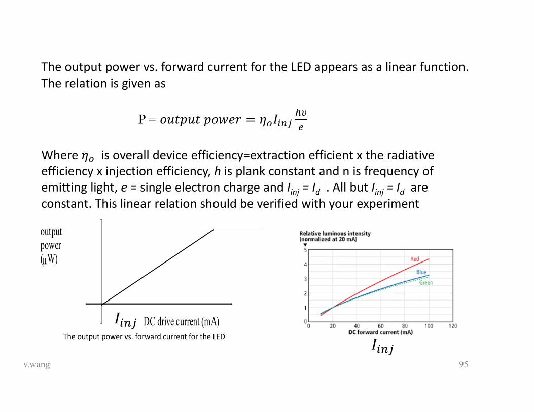
The output power vs. forward current for the LED appears as a linear function. The relation is given as
P =
Where is overall device efficiency=extraction efficient x the radiative efficiency x injection efficiency, h is plank constant and n is frequency of emitting light, e = single electron charge and Iinj = Id . All but Iinj = Id are constant. This linear relation should be verified with your experiment
DC drive current (mA)
outputpower(W)
The output power vs. forward current for the LED
w.wang 95

w.wang 96
Junction capacitance of the LED The dominant factors for rapid LED switching are not just the LED's inherent emission transition times:• Inductance of the traces causes longer rise and fall times. Longer traces = slower
transitions.• Junction capacitance of the LED itself is a factor(#2). For instance, 5mm through-hole
LEDs have a junction capacitance of 50 pF nominal. Smaller junctions e.g. 0602 SMD LEDs have correspondingly lower junction capacitance, and are in any case more likely to be used for screen backlights.
• Parasitic capacitance (traces and support circuitry) plays an important role in increasing the RC time constant and thus slowing transitions.
• Typical LED driving topologies e.g. low-side MOSFET switching, do not actively pull the voltage across the LED down when turning off, hence turn-off times are typically slower than turn-on.
• As a result of the inductive and capacitive factors above, the higher the forward voltage of the LED, the longer the rise and fall times, due to the power source having to drive current harder to overcome these factors. Thus IR LEDs, with typically the lowest forward voltages, transition fastest.

w.wang 97
C=A/W
W = [2rVbi-VA)(NA+ND)/(q NAND)]1/2

w.wang
There are two basic types of LED structures: edge emitters and surface emitters.
output power is high (emitting spot is very small, typically 30‐50 µm)
narrow emission spectra (FWHM is typically about 7% of the central wavelength)
Narrow beam pattern
simple structure, are relatively inexpensive, offer low‐to‐moderate output power levels, and are capable of low‐to‐moderate operating speeds
output power is as high or higher than the edge‐emitting LED, but the emitting area is large, causing poor coupling efficiency to the optical fiber
emit light in all directions
LEDP = P0 cos
98

Using the setup as shown in Figure., where the current is provided by the voltage source V is limited by the series resistance R. Under operating conditions, the voltage drop across the LED is Vd , the operating voltage of the device. If operating current is I=Id , then the circuit can be described by
w.wang 99
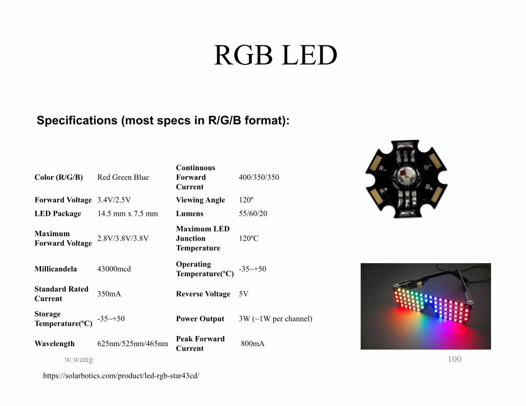
Color (R/G/B) Red Green BlueContinuous Forward Current
400/350/350
Forward Voltage 3.4V/2.5V Viewing Angle 120º
LED Package 14.5 mm x 7.5 mm Lumens 55/60/20
Maximum Forward Voltage 2.8V/3.8V/3.8V
Maximum LED Junction Temperature
120ºC
Millicandela 43000mcd Operating Temperature(ºC) -35~+50
Standard Rated Current 350mA Reverse Voltage 5V
Storage Temperature(ºC) -35~+50 Power Output 3W (~1W per channel)
Wavelength 625nm/525nm/465nm Peak Forward Current 800mA
Specifications (most specs in R/G/B format):
RGB LED
https://solarbotics.com/product/led-rgb-star43cd/
w.wang 100
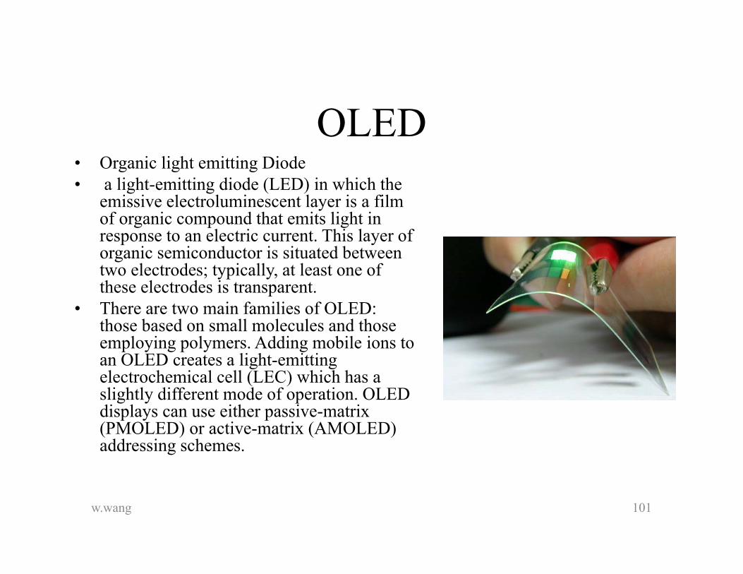
OLED• Organic light emitting Diode• a light-emitting diode (LED) in which the
emissive electroluminescent layer is a film of organic compound that emits light in response to an electric current. This layer of organic semiconductor is situated between two electrodes; typically, at least one of these electrodes is transparent.
• There are two main families of OLED: those based on small molecules and those employing polymers. Adding mobile ions to an OLED creates a light-emitting electrochemical cell (LEC) which has a slightly different mode of operation. OLED displays can use either passive-matrix (PMOLED) or active-matrix (AMOLED) addressing schemes.
w.wang 101

w.wang
Fiber Optic Sources
Two basic light sources are used for fiber optics: lasers and light-emitting diodes (LED). Each device has its own advantages and disadvantages as listed in Table
Characteristic LED Laser
Output power Lower Higher
Spectral width Wider Narrower
Numerical aperture Larger Smaller
Speed Slower Faster
Cost Less More
Ease of operation Easier More difficult
A. Guenther UCONN102
Both LED and solid state laser are diodes!

w.wang
Output Power Linearly proportional to drive current Proportional to current above the threshold
Current Drive Current: 50 to 100 mA Peak Threshold Current: 5 to 40 mA
Coupled Power Moderate High
Speed Slower Faster
Output Pattern Higher Lower
Bandwidth Moderate HighWavelengths Available 0.66 to 1.65 µm 0.78 to 1.65 µm
Spectral Width Wider (40-190 nm FWHM) Narrower (0.00001 nm to 10 nm FWHM)
Fiber Type Multimode Only SM, MM
Ease of Use Easier Harder
Lifetime Longer Long
Cost Low ($5-$300) High ($100-$10,000)A. Guenther UCONN103

Laser
w.wang 104

w.wang
LASER
LASAER = light amplification by stimulated emission of radiation
Invented dated to 1958 with the publication of the scientific paper, Infrared and Optical Masers, by Arthur L. Schawlow, then a Bell Labs researcher, and Charles H. Townes, a consultant to Bell Labs
105

w.wang
Property of Laser Light
• Nearly"monochromatic: consists of an extremely narrowrange of wavelengths (etrem narrow band)
• Highly Directional: travel in a single direction within a narrow cone of divergence
• Highly Coherence: coherence is the most fundamental property of laser light and distinguishes it from the lightfrom other sources
106

w.wang
Coherence
For longitudinal or temporal coherence, the coherence length C is related to the wavelength and the total frequency bandwidth of the laser by
Note: is the actual bandwidth of the laser beam given in wavelength units.
For transverse or spatial coherence, the transverse coherence length t is related to the laser wavelength , the laser source diameter at its origin s, and the distance r the beam has propagated from its origin, by the following relationship.
107

w.wang 108
Two sources of light are said to be coherent if the waves emitted from them have the same frequency and are 'phase-linked'; that is, they have a zero or constant phase difference.
Coherence
Out of phase of same wavelength or different wavelengths

w.wang 109
Two sources of light are said to be coherent if the waves emitted from them have the same frequency and are 'phase-linked'; that is, they have a zero or constant phase difference.
Coherence
w.wang 110
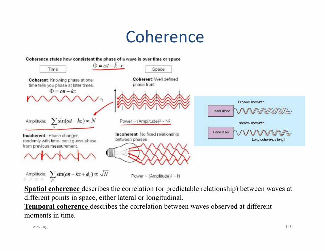
Coherence
Spatial coherence describes the correlation (or predictable relationship) between waves at different points in space, either lateral or longitudinal. Temporal coherence describes the correlation between waves observed at different moments in time.

Temporal Coherence
w.wang 111
Temporal coherence is a measure of the correlation between the phases of a light wave at different points along the direction of propagation. Temporal coherence tells us how monochromatic a source is.
Assume our source emits waves with wavelength λ ± Δλ. Waves with wavelength λ and λ + Δλ, which at some point in space constructively interfere, will no longer constructively interfere after some optical path length lc = λ2/(2πΔλ); lc is called the coherence length.
The phase of a wave propagating into the x-direction is given by φ = kx - ωt. Look at the wave pattern in space at some time t. At some distance l, the phase difference between two waves with wave vectors k1 and k2 which are in phase at x = 0 becomes Δφ = (k1 - k2)l. When Δφ = 1 (rad), or Δφ ~ 60o, the light is no longer considered coherent. Interference and diffraction patterns severely loose contrast.We therefore have1 = (k1 - k2)lc = (2π/λ - 2π/(λ + Δλ))lc.(λ + Δλ - λ)lc/(λ(λ + Δλ)) ~ Δλlc/λ2 = 1/2π.
lc = λ2/(2πΔλ)
sinA+sinB = 2sin(A+B)/2 *cos(A-B)/2
Let A = k1x+1t k1 = n1
B = k2x+2t k2 = n2
lc
z
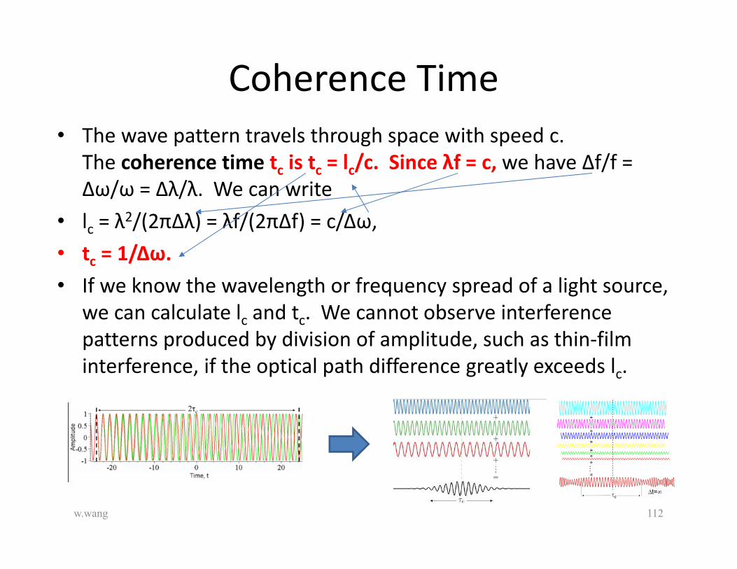
Coherence Time • The wave pattern travels through space with speed c.
The coherence time tc is tc = lc/c. Since λf = c, we have Δf/f = Δω/ω = Δλ/λ. We can write
• lc = λ2/(2πΔλ) = λf/(2πΔf) = c/Δω,• tc = 1/Δω.• If we know the wavelength or frequency spread of a light source,
we can calculate lc and tc. We cannot observe interference patterns produced by division of amplitude, such as thin‐film interference, if the optical path difference greatly exceeds lc.
w.wang 112

Spatial Coherence
w.wang 113
Spatial coherence is a measure of the correlation between the phases of a lightwave at different points transverse to the direction of propagation. Spatialcoherence tells us how uniform the phase of the wave front is. A distance Lfrom a thermal monochromatic (line) source whose linear dimensions are on theorder of δ, two slits separated by a distance greater than dc = 0.16λL/δ will nolonger produce a recognizable interference pattern. We call πdc
2/4 the coherencearea of the source.
A wave with a varying profile (wavefront) and infinite coherence length
A wave with a varying profile (wavefront) and finite coherence length.
A wave with finite coherence area is incident on a pinhole (small aperture). The wave will diffract out of the pinhole. Far from the pinhole the emerging spherical wavefronts are approximately flat. The coherence area is now infinite while the coherence length is unchanged.
A plane wave with an infinite coherence length.

w.wang 114
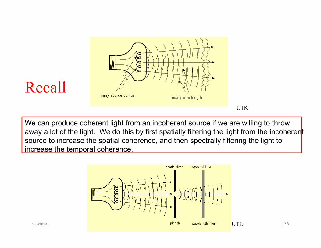
We can produce coherent light from an incoherent source if we are willing to throw away a lot of the light. We do this by first spatially filtering the light from the incoherent source to increase the spatial coherence, and then spectrally filtering the light to increase the temporal coherence.
UTK
UTK
Solution for spatial incoherent
Spatial Coherence
w.wang 115
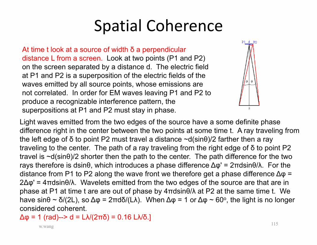
At time t look at a source of width δ a perpendicular distance L from a screen. Look at two points (P1 and P2) on the screen separated by a distance d. The electric field at P1 and P2 is a superposition of the electric fields of the waves emitted by all source points, whose emissions are not correlated. In order for EM waves leaving P1 and P2 to produce a recognizable interference pattern, the superpositions at P1 and P2 must stay in phase.
Light waves emitted from the two edges of the source have a some definite phase difference right in the center between the two points at some time t. A ray traveling from the left edge of δ to point P2 must travel a distance ~d(sinθ)/2 farther then a ray traveling to the center. The path of a ray traveling from the right edge of δ to point P2 travel is ~d(sinθ)/2 shorter then the path to the center. The path difference for the two rays therefore is dsinθ, which introduces a phase difference Δφ' = 2πdsinθ/λ. For the distance from P1 to P2 along the wave front we therefore get a phase difference Δφ = 2Δφ' = 4πdsinθ/λ. Wavelets emitted from the two edges of the source are that are in phase at P1 at time t are are out of phase by 4πdsinθ/λ at P2 at the same time t. We have sinθ ~ δ/(2L), so Δφ = 2πdδ/(Lλ). When Δφ = 1 or Δφ ~ 60o, the light is no longer considered coherent.Δφ = 1 (rad)--> d = Lλ/(2πδ) = 0.16 Lλ/δ.]

Why Coherent Length is important?
w.wang 116
Additional modulation or interference du to incoherent light behave just like grating diffraction effect due to phase difference or like another inference due to phase difference between wavelengths (in this case due to wavelength difference 2nd/
Coherence legth ~ Beats
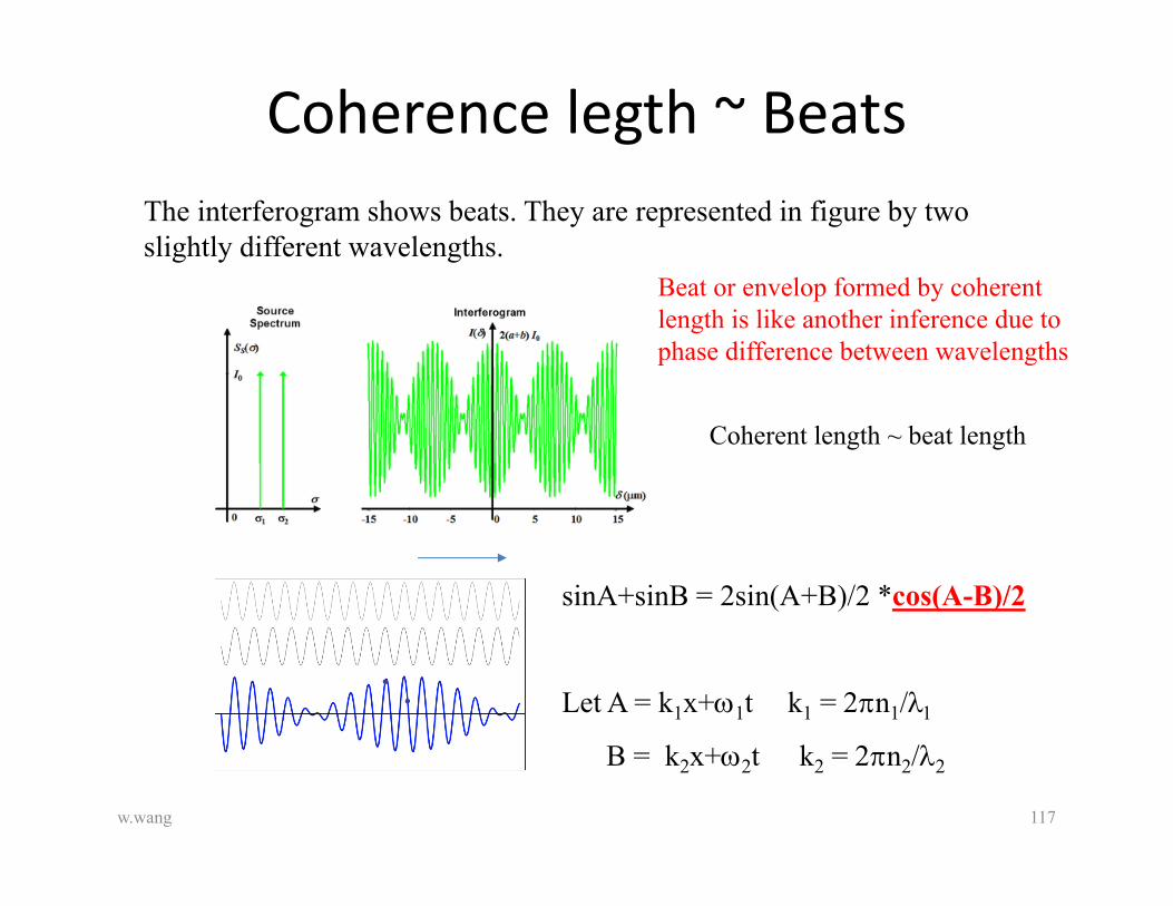
w.wang 117
The interferogram shows beats. They are represented in figure by two slightly different wavelengths.
sinA+sinB = 2sin(A+B)/2 *cos(A-B)/2
Let A = k1x+1t k1 = n1
B = k2x+2t k2 = n2
Coherent length ~ beat length
Beat or envelop formed by coherent length is like another inference due to phase difference between wavelengths

118
If there are more than two wavelength in case of a broadband light source, then the sumOf all wavelengths in time domain is shown as
Coherence and Beats (example)
lc = λo2/(2πnΔλ) lc = (2ln2/)(λo
2/(2πnΔλ))
Only within coherent length you can see interference!
Recall
+++W. Wang This is multiwavelength interference!!!!
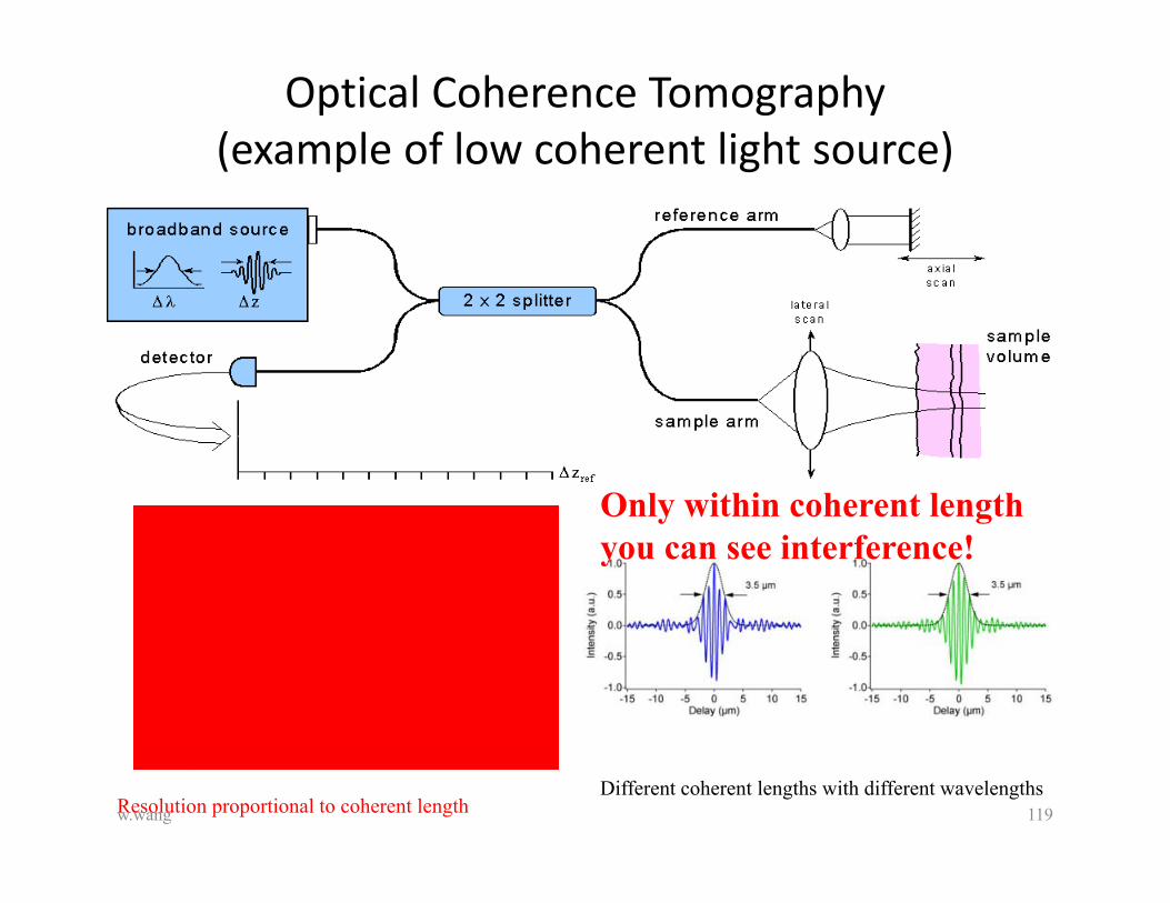
Optical Coherence Tomography(example of low coherent light source)
Different coherent lengths with different wavelengths
Only within coherent length you can see interference!
Resolution proportional to coherent lengthw.wang 119

w.wang 120
The resolution of OCT in the A-line direction is determined by the bandwidth of the laser source and is typically on the order of 10 µm, sufficient for resolving tissue layers and larger morphological structures. Imaging depth in OCT is limited by the optical transparency (absorption and scattering) of the tissue but is typically on the order of 1 to 2 mm.
Time Domain Optical Coherence Tomography

Double interference from double mirrors
Recall
+++ Fix
mirror
W. Wang
The combination of reflected light from the sample arm and reference light from the reference arm gives rise to an interference pattern, but only if light from both arms have traveled the "same" optical distance ("same" meaning a difference of less than a coherence length). Any light that is outside the short coherence length will not interfere.
x =Moving mirror+ fix mirror Output signalBroadband source
looklikethiscos cos ) = output but correct equation should looks like
) = output
Look at matlab program

Double interference
w wang
122
Recall
+++
x =Moving mirror + sample Output signalBroadband source
) = output
mirror
The combination of reflected light from the sample arm and reference light from the reference arm gives rise to an interference pattern, but only if light from both arms have traveled the "same" optical distance ("same" meaning a difference of less than a coherence length). Any light that is outside the short coherence length will not interfere. Each sample location will create its own interference within coherent length due to moving mirror
R1,R2,R3R1, R2, R3
Z

w.wang 123
The light incident on the tissue will undergo backreflection and backscattering from multiple sites due the presence of scattering particles and refractive index variations within the tissue. The backscattered photons returning from the sample arm can be described as the convolution of the incident field and the backscattering function and can be written as
The reference arm typically has a variable attenuator or neutral density filter to adjust the reference light power level. The attenuated electric field reflected by the reference mirror is given as
If we assume a wavelength-independent splitting ratio for the coupler or beam-splitter, then the broadband source light output propagating into each arm of the interferometer can be written as:
where rS(z) is the depth-dependent amplitude reflectivity function of the sample. The sample and reference electric fields are recombined at the beamsplitter and are given by

w.wang 124
The incident light is then converted into photo-current by optical detectors, which are square law intensity detection devices. The generated photo-current is proportional to the time average of the incident electric field multiplied by its complex conjugate and is given by:
where ρ is the detector responsivity (Ampere/Watt) and S(k) = |s(k)|2 is the normalized spectral power density of the source. The first two terms on the right hand side of the equation represent the DC component of the current and self interference. The final term in this equation accounts for the interference between the reference and sample electric fields and is used to extract the axial depth profile or structural information in OCT. When simplified, the AC component of the photocurrent can be written as follows:
The goal of various OCT signal processing techniques is to extract the depth-dependent reflectivity function (RS (Δz)) of the sample in order to obtain its axial structural profile information.
w.wang 125
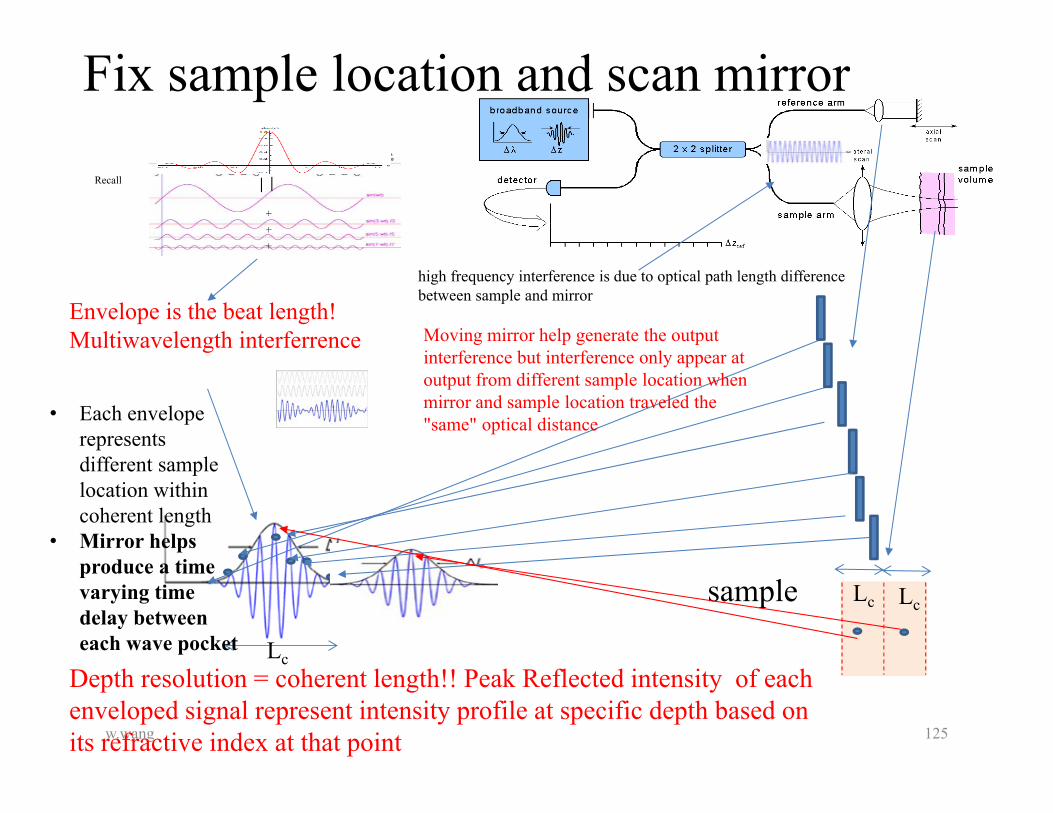
sample Lc
high frequency interference is due to optical path length difference between sample and mirror
Envelope is the beat length!Multiwavelength interferrence
Depth resolution = coherent length!! Peak Reflected intensity of each enveloped signal represent intensity profile at specific depth based on its refractive index at that point
Lc
Lc
Recall
+++
Moving mirror help generate the output interference but interference only appear at output from different sample location when mirror and sample location traveled the "same" optical distance
Fix sample location and scan mirror
• Each envelope represents different sample location within coherent length
• Mirror helps produce a time varying time delay between each wave pocket

w.wang 126
sample Lc
Lc
Lc
Moving mirror help generate the output interference but interference only appear at output from different sample location when mirror and sample location traveled the "same" optical distance
Lc/2 after bue line reflection
Lc/2 before blue line reflection
Point on interference curve is combination of many reflections from sample and mirror. Wave packet is also formed by light source multiwavelengths
Fix mirror location and scan different sample location
• Each envelope represents different sample location within coherent length• Mirror helps produce a time varying time delay beatween each pocket
How Beat amplitude is modulated
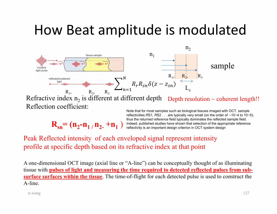
w.wang 127
Peak Reflected intensity of each enveloped signal represent intensity profile at specific depth based on its refractive index at that point
Refractive index n2 is different at different depthReflection coefficient:
Rsn= (n2-n1 / n2- +n1 )
samplen1
n2
Depth resolution ~ coherent length!!
Lc
A one-dimensional OCT image (axial line or “A-line”) can be conceptually thought of as illuminating tissue with pulses of light and measuring the time required to detected reflected pulses from sub-surface surfaces within the tissue. The time-of-flight for each detected pulse is used to construct the A-line.
Note that for most samples such as biological tissues imaged with OCT, sample reflectivities RS1, RS2 . . . are typically very small (on the order of ∼10−4 to 10−5); thus the returned reference field typically dominates the reflected sample field. Indeed, published studies have shown that selection of the appropriate reference reflectivity is an important design criterion in OCT system design
R1, R2, R3
R1, R2, R3

x=
w.wang 128
sample
Lc
Envelope is the beat length!
Depth resolution = coherent length!! Peak Reflected intensity of each enveloped signal represent intensity profile at specific depth based on its refractive index at that point
Beat or envelop formed by coherent length is like another inference due to phase difference between wavelengths
moving mirror + sample interference!
R1,R2,R3
R1, R2, R3
cos2π Δ
∆∆
) lc = (2ln2/)(λo2/(2πnΔλ))

w.wang 129
x=
w.wang
Envelope is the beat length!
Depth resolution = coherent length!! Peak Reflected intensity of each enveloped signal represent intensity profile at specific depth based on its refractive index at that point
Beat or envelop formed by coherent length is like another inference due to phase difference between wavelengths
Moving mirror +sample interference
R1,R2,R3
R1, R2, R3
lc = (2ln2/)(λo2/(2πnΔλ))cos
2π Δ∆
∆
)
w.wang 130
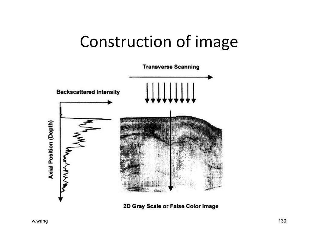
Construction of image
w.wang
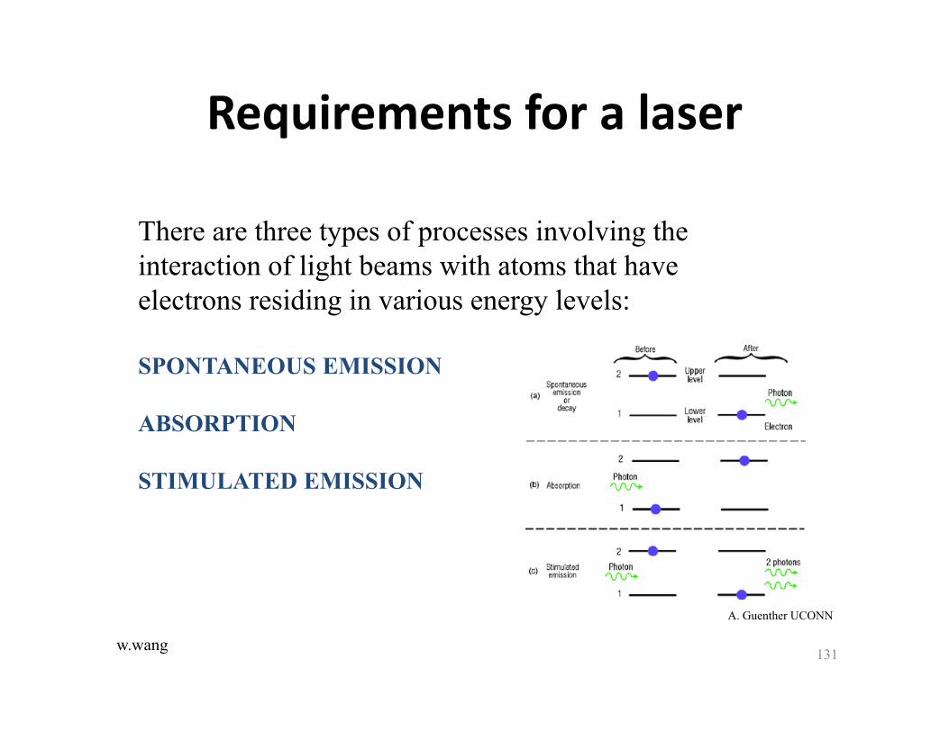
There are three types of processes involving the interaction of light beams with atoms that have electrons residing in various energy levels:
SPONTANEOUS EMISSION
ABSORPTION
STIMULATED EMISSION
Requirements for a laser
A. Guenther UCONN
131

w.wang
An atom in an excited state is unstable and will release spontaneously its excess energy and return to the ground state. This energy release may occur in a single transition or in a series of transitions that involve intermediate energy levels. For example, an atom in state E3 could reach the ground state by means of a single transition from E3 to El, or by two transitions, first from E3 to E2 and then from E2 to E1. In any downward atomic transition, an amount of energy equal to the difference in energy content of the two levels must be released by the atom.
SPONTANEOUS EMISSION
A. Guenther UCONN
132

w.wang
Most excited energy levels undergo spontaneous emission. Each level has a specific lifetime over which it will remain in that level before decaying to a lower-lying level. That lifetime is determined by the interactions of the electron with the other electrons and nuclei of that atom. Typical lifetimes of electrons residing in specific levels that decay by radiating in the visible portion of the spectrum are of the order of 10–100 nsec. The photon radiated during spontaneous emission has the exact wavelength 21 and frequency 21corresponding to the difference in energy E21 of the two involved energy levels (1 and 2 in this case) according to the relationship
E21 = h21 =
in which h is Planck’s constant such that h = 6.63 × 10⁻³⁴ joule-sec and c is the speed of light, c = 3 × 10⁸ m/sec.
Because different materials have different energy-level arrangements, they radiate at different wavelengths and thus emit different colors or frequencies of light that are specific to the material.
133
w.wang
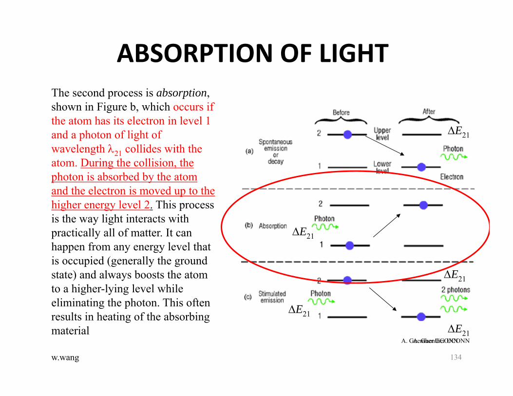
The second process is absorption, shown in Figure b, which occurs if the atom has its electron in level 1 and a photon of light of wavelength 21 collides with the atom. During the collision, the photon is absorbed by the atom and the electron is moved up to the higher energy level 2. This process is the way light interacts with practically all of matter. It can happen from any energy level that is occupied (generally the ground state) and always boosts the atom to a higher-lying level while eliminating the photon. This often results in heating of the absorbing material
ABSORPTION OF LIGHT
A. Guenther UCONNA. Guenther UCONNE21
E21
E21
E21
E21
134

w.wang
When a large group of atoms is assembled and irradiated with light, most of those atoms are in the ground-state energy level. If the photons of the impinging light have the appropriate energy E20 for example, the light will be absorbed according to the following expression for the variation of intensity I with the distance L into the material (known as (Lambert Law):
Where I0 = intensity of the beam when it first reaches the atoms
20 = cross section for absorption or emission of those two levels (cm2),
N0 = population density of atoms residing in level 0 (atoms/cm3 ),
20 N0 = absorption coefficient
ABSORPTION
Intensity variation versus depth z into an absorbing sample
A. Guenther UCONN
135

w.wang
The third process, shown in Figure is referred to as stimulated emission. It results when an electron is in a higher-lying level, such as level 2, and a photon of light of wavelength 21collides with the atom. During the collision the photon stimulates the atom to radiate a second photon having exactly the same energy E21 as that of the incident photon and traveling in exactly the same direction in order to satisfy the laws of conservation of energy and momentum. Hence, one photon leads to two identical photons, which, in effect, leads to an amplification process. A photon has been gained at the expense of the loss of energy stored within the atom.
Stimulated Emission
A. Guenther UCONN
E21
E21
E21
E21
E21
136

w.wang
Suppose that we were able to “pump” (excite) a significant amount of population of the medium from level 0 to level 2. Also, for the time being let us assume that there is no population in level 1. (This is an unlikely scenario but we will do this as a “thought” experiment for illustrative purposes.) Then again, let us consider having a beam of photons of energy E21 and wavelength 21 enter the medium. According to the earlier discussion, and considering the process that can occur is stimulated emission, and we would expect more photons to be generated as the beam progresses. This can be described mathematically in the equation below
in which we now have the population density N2 in the expression along with the appropriate cross section 21.
Stimulated Emission
137
w.wang
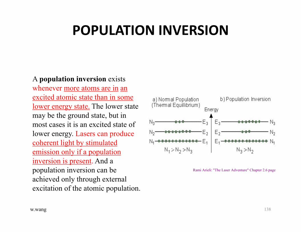
POPULATION INVERSION
A population inversion exists whenever more atoms are in an excited atomic state than in some lower energy state. The lower state may be the ground state, but in most cases it is an excited state of lower energy. Lasers can produce coherent light by stimulated emission only if a population inversion is present. And a population inversion can be achieved only through external excitation of the atomic population.
Rami Arieli: "The Laser Adventure" Chapter 2.6 page
138
w.wang
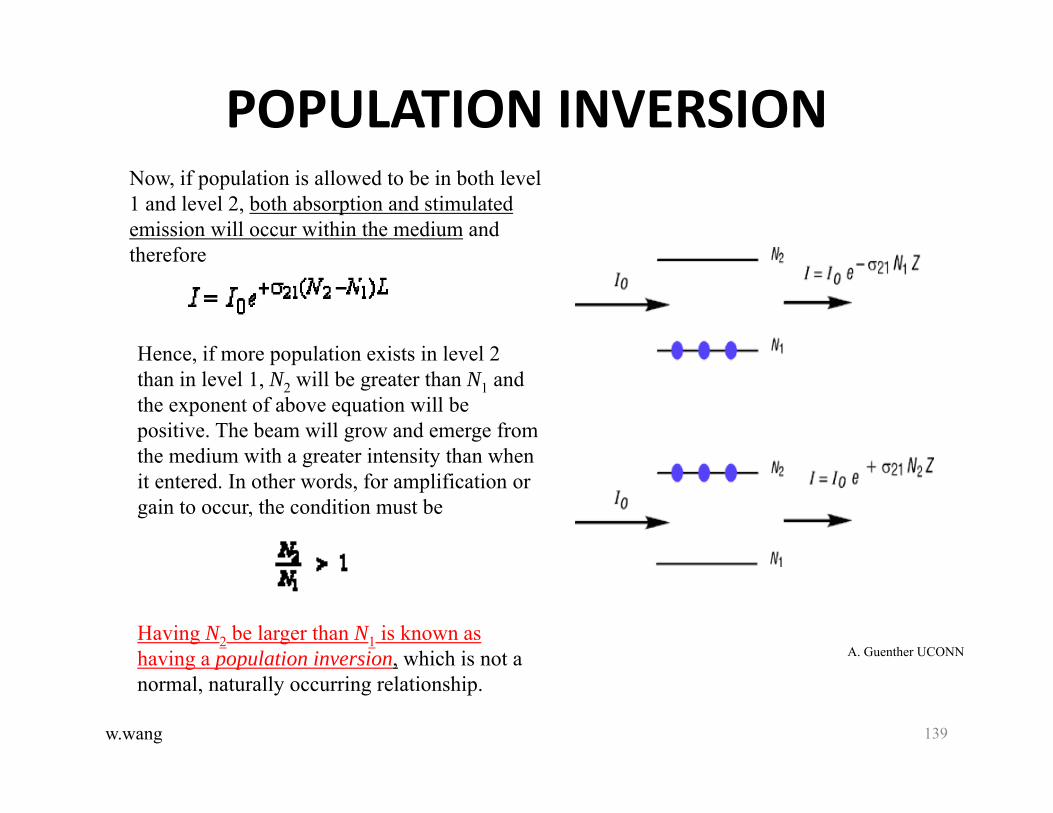
Now, if population is allowed to be in both level 1 and level 2, both absorption and stimulated emission will occur within the medium and therefore
Hence, if more population exists in level 2 than in level 1, N2 will be greater than N1 and the exponent of above equation will be positive. The beam will grow and emerge from the medium with a greater intensity than when it entered. In other words, for amplification or gain to occur, the condition must be
Having N2 be larger than N1 is known as having a population inversion, which is not a normal, naturally occurring relationship.
POPULATION INVERSION
A. Guenther UCONN
139

w.wang
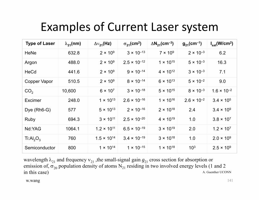
It is useful to describe the product of 21 and N21 as the small-signal-gain coefficient g21 or g21 = 21N21
By considering the units of both 21 (length2) and N21 (l/length3) we can see that g21 has the units of 1/length. Hence, if 21 is given in units of cm2 and N21 is given in units of (1/cm3), g21 will be given in (1/cm), more commonly expressed as cm–1. Values of the cross sections 21 and N21, and the small-signal gain g21
Small‐signal‐gain coefficient
140
w.wang
Type of Laser 21(nm) 21(Hz) 21(cm2) N21(cm–3) g21(cm–1) Isat(W/cm2)
HeNe 632.8 2 × 10⁹ 3 × 10–13 7 × 10⁹ 2 × 10⁻³ 6.2
Argon 488.0 2 × 10⁹ 2.5 × 10⁻¹² 1 × 10¹⁵ 5 × 10⁻³ 16.3
HeCd 441.6 2 × 10⁹ 9 × 10–14 4 × 10¹² 3 × 10⁻³ 7.1
Copper Vapor 510.5 2 × 10⁹ 8 × 10–14 6 × 10¹³ 5 × 10⁻² 9.0
CO2 10,600 6 × 10⁷ 3 × 10–18 5 × 10¹⁵ 8 × 10⁻³ 1.6 × 10⁻²
Excimer 248.0 1 × 10¹³ 2.6 × 10⁻¹⁶ 1 × 10¹⁶ 2.6 × 10⁻² 3.4 × 10⁵
Dye (Rh6-G) 577 5 × 10¹³ 2 × 10–16 2 × 10¹⁸ 2.4 3.4 × 10⁹
Ruby 694.3 3 × 10¹¹ 2.5 × 10⁻²⁰ 4 × 10¹⁹ 1.0 3.8 × 10⁷
Nd:YAG 1064.1 1.2 × 10¹¹ 6.5 × 10⁻¹⁹ 3 × 10¹⁹ 2.0 1.2 × 10⁷
Ti:Al2O3 760 1.5 × 10¹⁴ 3.4 × 10⁻¹⁹ 3 × 10¹⁸ 1.0 2.0 × 10⁹
Semiconductor 800 1 × 10¹⁴ 1 × 10–15 1 × 10¹⁸ 103 2.5 × 10⁹
A. Guenther UCONN
Examples of Current Laser system
141
wavelength 21 and frequency 21 ,the small-signal gain g21 cross section for absorption or emission of, 20 population density of atoms N21 residing in two involved energy levels (1 and 2 in this case)

w.wang
Laser gain mediumAtoms such as in the red helium-neon (HeNe) laser, the visible and ultraviolet argon ion and helium-cadmium (HeCd) lasers, and the green and yellow copper vapor lasers (CVL)
Molecules such as in the infrared carbon dioxide (CO2) laser, the ultraviolet excimer lasers such as ArF and KrF, and the pulsed N2 laser
Liquids such as those involving various organic dye molecules dilute dissolved in various solvent solutions
Dielectric solids such as those involving neodymium atoms doped in YAG or glass to make the crystalline Nd:YAG or Nd:glass lasers
Semiconductor materials such as gallium arsenide or indium phosphide crystals or various mixtures of impurities blended with those and other semiconductor species
142

w.wang
Population Inversion in lasing mediums
A. Guenther UCONN
143
- Gas (inert gas)- Liquid (pump source)- Solid state (pump source)- Semiconductor (PN junction)

w.wang
ATOM MOLECULE ION
•He-Ne (Helium-Neon)
Metal Vapor Lasers•Cu (Copper) Vapor•Au (Gold) Vapor
Ionized vapor Lasers*He-Cd (Helium-Cadmium)
•CO2 (Carbon Dioxide)•N2 (Nitrogen)•Chemical (HF-DF)•FIR - Far Infrared•Excimer Laser
•Ar+ (Argon ion)•Kr+ (Krypton ion)
Gas Laser
144
Within gas lasers, they are divided into 3 different types:

w.wang
- Applied voltage produces an electric field accelerates the electrons within the gas.
- Excited electrons collide with the gas atoms and excite the atoms to excited energylevels, some of which serve as upper laser levels.
- Lower-lying levels, those to which higher-lying levels can transition, typically decay to the ground state faster than the higher-lying levels, thereby establishing a population inversion between some of the higher and lower levels.
- The laser light then occurs when the higher-lying levels decay to the lower levelswhile radiating photons at the wavelengths corresponding to the energy separation between the levels.
- In many instances the excitation is a two-step process in which the electrons * first excite a long-lived or metastable (storage) level or they ionize the atom,
leaving an ion of that species and another electron. In either case, that level * then transfers its stored energy to the upper laser level via a subsequent
collision with the laser species.
Population Inversion in gas laser
145

w.wang
Gas laser
A. Guenther UCONN
One popular type of gas laser contains a mixture of helium (He) and neon (Ne) gases and is illustrated in Figure. The gas mixture is contained at a low pressure within a sealed glass tube called the "plasma tube. The feedback mechanism consists of a pair of mirrors sealed to the ends of the plasma tube. One of these mirrors, the output coupler, transmits 1-2 percent of the light to form a continuous (CW) output beam.
146

Why the laser light is monochromatic?
• Laser light consists of essentially one wavelength, having its origin in stimulated emission from one set of atomic energy levels. This is possible because laser transition, in principle, involves well‐defined energy levels.
• EM wave of frequency n = (E2 ‐ E1) only can be amplified, n has a certain range which is called line width. This line width is decided by various broadening factors such as Doppler effect of moving atoms and molecules.
• The generation of laser is such that the laser cavity forms a resonant system and laser oscillation is sustained only at the resonant frequencies of the cavity. This leads to the further narrowing of the laser line width. So laser light is usually very pure in wavelength, we say it has the property of monochromatic
w.wang 147

Laser Cavity
w.wang 148

How spectral filter created by mirror cavity
w.wang 149

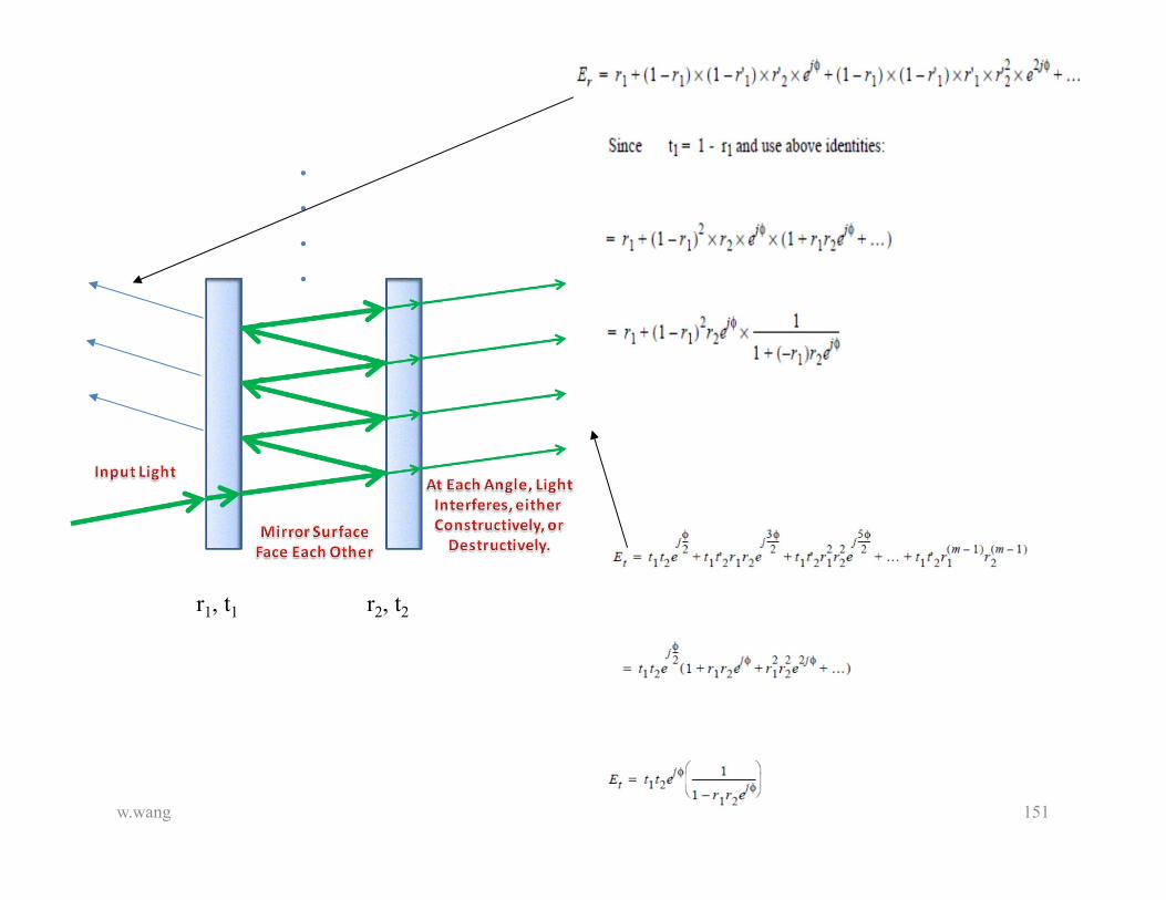
Fabry‐Perot Interferometer
Interference of an infinite number of waves progressively smaller amplitude and equal phase difference.
w.wang 150
w.wang 151
.
.
.
.
r1, t1 r2, t2
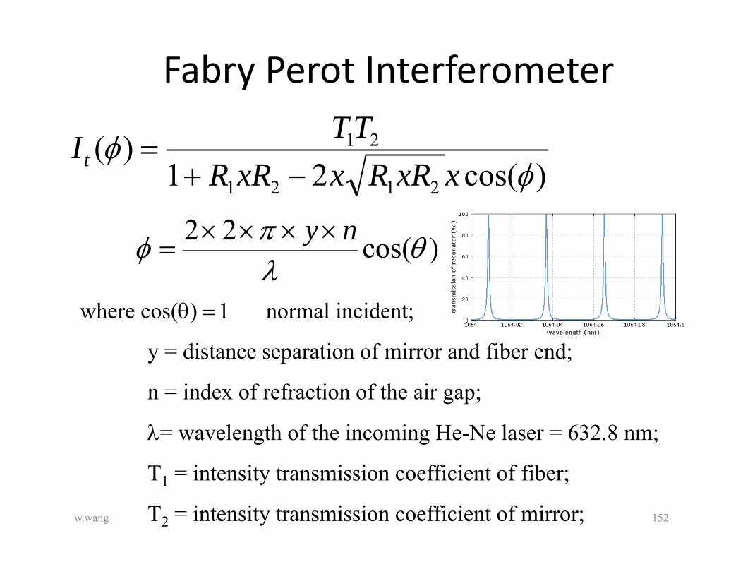
Fabry Perot Interferometer
)cos(21)(
2121
21
xxRRxxRRTTIt
where cos(normal incident;
y = distance separation of mirror and fiber end;
n = index of refraction of the air gap;
= wavelength of the incoming He-Ne laser = 632.8 nm;
T1 = intensity transmission coefficient of fiber;
T2 = intensity transmission coefficient of mirror;
)cos(22 ny
w.wang 152

Refection Intensity
)cos(21))cos(2()(
2121
2121
xxRRxxRR
xRRxRRIr
)cos(22 ny
where cos(normal incident;
y = distance separation of mirror and fiber end;
n = index of refraction of the air gap;
= wavelength of the incoming He-Ne laser = 632.8 nm;
R1 = intensity reflection coefficient of fiber;
R2 = intensity reflection coefficient of mirror;w.wang 153

Finesse
This parameter is defined as the ratio of the half power bandwidth over the peak to peak full bandwidth. It’s a way to measure the sharpness of the curve.
22 f
2
)1(4
221
21
f
RRRRf
Where = half power bandwidth
w.wang 154

Transmission SpectrumThe frequency of each line is given by
f = p Co/(2nycos) where p = +1, +2, +3,…
The lines are separated in frequencies by
f = Co/(2nycos) The spacing between etalon modes is
= f 2/Co
The mode number of the etalon is
p = f/fw.wang 155
w.wang 156
We can produce coherent light from an incoherent source if we are willing to throw away a lot of the light. We do this by first spatially filtering the light from the incoherent source to increase the spatial coherence, and then spectrally filtering the light to increase the temporal coherence.
UTK
UTK
Recall
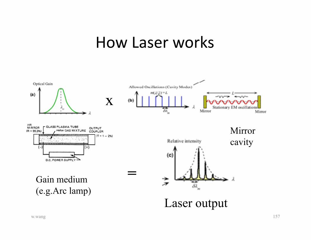
How Laser works
w.wang 157
x
=
Laser output
Gain medium(e.g.Arc lamp)
Mirror cavity

w.wang
Laser structure
A. Guenther UCONN 158

w.wang A. Guenther UCONN 159

w.wang
For a laser in which the amplifier length has a value of L and the mirrors have identical reflectivities R, with no other losses in the cavity, the threshold condition for the gain coefficient g is given as
which has dimensions of 1/length. Any value of g higher than above equation will produce a laser beam within the cavity. For a more complex laser cavity in which the mirrors have different reflectivities R1 and R2, and a1 and a2 represent other losses within the cavity (beyond the amplifier), the expression for the threshold gain g is given as
The term represents a potential absorption loss within the amplifier itself, which is present in only a few types of lasers. It is a distributed loss expressed in the same units as g or (1/length). For example, in solid-state lasers it is termed excited state absorption.
Gain coefficient
160

w.wang
Laser gain bandwidths for the HeNe, Nd:YAG, and Ti:Al2O3 lasers
Bandwidth of laser gain medium
The bandwidth of the laser gain medium determines the range of wavelengths over which amplification can occur for any specific laser. This bandwidth is expressed in either a wavelength range G or a frequency range vG. These two expressions are related by
in which is the laser wavelength and c is the speed of light. The bandwidth of the gain medium is usually determined by the bandwidth over which the spontaneous emission occurs for a given laser transition.
A. Guenther UCONN
161
Full width at half maximum (FWHM)

w.wang
Coherence
For longitudinal or temporal coherence, the coherence length C is related to the wavelength and the total frequency bandwidth of the laser by
Note: is the actual bandwidth of the laser beam given in wavelength units.
For transverse or spatial coherence, the transverse coherence length t is related to the laser wavelength , the laser source diameter at its origin s, and the distance r the beam has propagated from its origin, by the following relationship.
162

w.wang
ATOM MOLECULE ION
•He-Ne (Helium-Neon)
Metal Vapor Lasers•Cu (Copper) Vapor•Au (Gold) Vapor
Ionized vapor Lasers*He-Cd (Helium-Cadmium)
•CO2 (Carbon Dioxide)•N2 (Nitrogen)•Chemical (HF-DF)•FIR - Far Infrared•Excimer Laser
•Ar+ (Argon ion)•Kr+ (Krypton ion)
Gas Laser
163
Within gas lasers, they are divided into 3 different types:
Atom Lasers
w.wang 164

w.wang
HeNe laser
Discharge electrons flowing from the cathode toward the anode.
A helium–neon laser or HeNe laser, is a type of gas laser whose gain medium consists of a mixture of helium and neon(10:1) inside of a small bore capillary tube, usually excited by a DC electrical discharge. The best-known and most widely used HeNe laser operates at a wavelength of 632.8 nm, in the red part of the visible spectrum.The current pumps the helium atoms to an excited atomic state. The energy of the excited helium atoms is transferred to neon atoms through collisions, and the neon atoms then undergo a transition to a lower energy state that results in lasing.
A. Guenther UCONN 165
w.wang
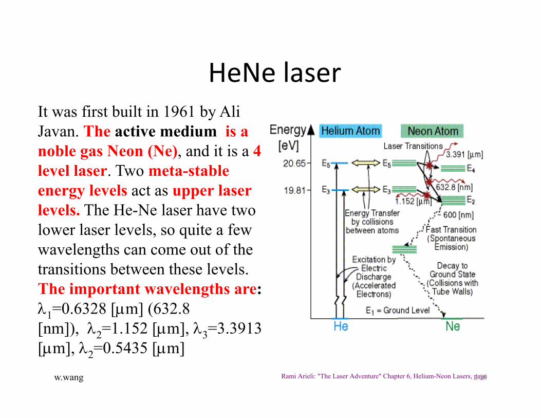
It was first built in 1961 by Ali Javan. The active medium is a noble gas Neon (Ne), and it is a 4 level laser. Two meta-stable energy levels act as upper laser levels. The He-Ne laser have two lower laser levels, so quite a few wavelengths can come out of the transitions between these levels. The important wavelengths are:1=0.6328 [m] (632.8 [nm]), 2=1.152 [m], 3=3.3913 [m], 2=0.5435 [m]
Rami Arieli: "The Laser Adventure" Chapter 6, Helium-Neon Lasers, page
HeNe laser
166
w.wang 167
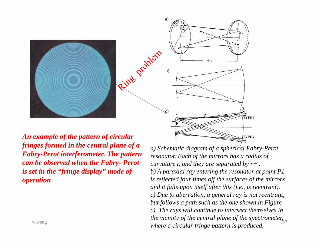
An example of the pattern of circular fringes formed in the central plane of a Fabry-Perot interferometer. The pattern can be observed when the Fabry- Perot is set in the “fringe display” mode of operation
a) Schematic diagram of a spherical Fabry-Perot resonator. Each of the mirrors has a radius of curvature r, and they are separated by r+ . b) A paraxial ray entering the resonator at point P1 is reflected four times off the surfaces of the mirrors and it falls upon itself after this (i.e., is reentrant). c) Due to aberration, a general ray is not reentrant, but follows a path such as the one shown in Figure c). The rays will continue to intersect themselves in the vicinity of the central plane of the spectrometer, where a circular fringe pattern is produced.
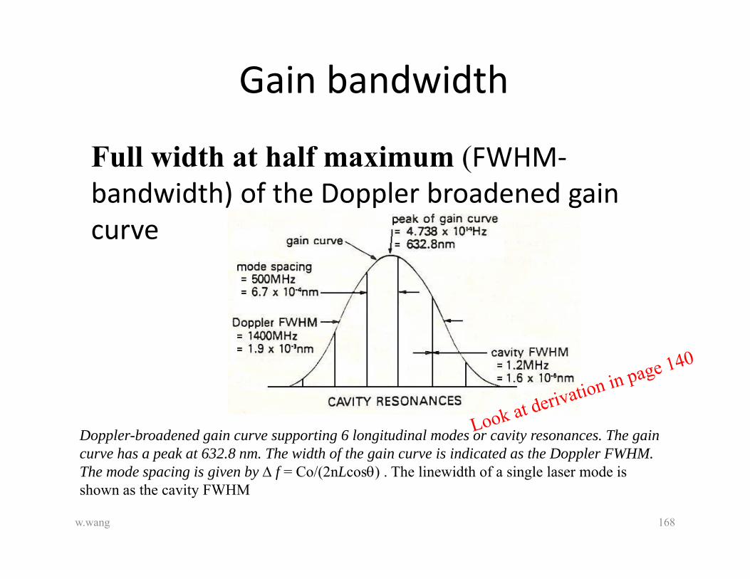
Gain bandwidth
Full width at half maximum (FWHM‐bandwidth) of the Doppler broadened gain curve
w.wang 168
Doppler-broadened gain curve supporting 6 longitudinal modes or cavity resonances. The gain curve has a peak at 632.8 nm. The width of the gain curve is indicated as the Doppler FWHM. The mode spacing is given by f = Co/(2nLcos) . The linewidth of a single laser mode isshown as the cavity FWHM

Free Spectral Range and Instrument bandwidth
What is the width of the spectrum ?, ?
c/ d (c / 2)d (c /
coherence‐ length
w.wang 169

Laser cavity modesIn practice, L is usually much greater than λ, so the relevant values of q are large (around 105 to 106). Of more interest is the frequency separation between any two adjacent modes q and q+1; this is given (for an empty linear resonator of length L) by Δν:
= c/ 2L
where c is the speed of light (≈3×10⁸ m∙s−1).Using the above equation, a small laser with a mirror separation of 30 cm has a frequency separation between longitudinal modes of 0.5 GHz. Thus for the two lasers referenced above, with a 30‐cm cavity, the 1.5 GHz bandwidth of the HeNe laser would support up to 3 longitudinal modes, whereas the 128 THz bandwidth of the Ti:sapphire laser could support approximately 250,000 modes. When more than one longitudinal mode is excited, the laser is said to be in "multi‐mode" operation. When only one longitudinal mode is excited, the laser is said to be in "single‐mode" operation.Each individual longitudinal mode has some bandwidth or narrow range of frequencies over which it operates, but typically this bandwidth, determined by the Q factor (see Inductor) of the cavity (see Fabry–Pérot interferometer), is much smaller than the intermode frequency separation
w.wang 170

Different Cavity Length
w.wang 171
A function of the cavity lengthf = Co/(2nycos)
Free spectral range (FSR) is the spacing in optical frequency or wavelength between two successive reflected or transmitted optical intensity maxima or minima of an interferometer
= f 2/Co
Metal Vapor Lasers
w.wang 172
w.wang
Helium‐Cadmium Laser
Rami Arieli: "The Laser Adventure" Chapter 6, Helium-Cadmium Lasers, page 1
Helium-Cadmium lasers can be categorized among either: •Metal vapor lasers - Cadmium is a metal, the lasing action in Helium Cadmium laser occurs between energy levels of Cadmium ions, so the lasing medium is ionized metal vapor. •Ion gas lasers - The properties of Helium-Cadmium laser are similar to those of Helium-Neon laser which is a neutral atom gas laser.
The He-Cd laser is a gas laser, and the metal Cadmium can be transform into the gas phase by heat. The excitation to the upper laser level of the Cadmium atoms in the gas is similar to the excitation process of the Neon gas in a Helium-Neon laser: Helium atoms are excited by collisions with accelerated electrons, and than they pass their energies to Cadmium atoms by collisions.
Thus, the main application of the He-Cd laser is in the optics laboratory, for fabricating holographic gratings. (UV, 351nm)
173

w.wang
This laser was attractive because of its relative high efficiency (up to 1%) for lasers in the visible spectrum range, and the high pulse power achieved.
Copper Vapor Laser Structure
Copper vapor laser is a gas laser, build as a tube with windows at both ends. The tube is filled with an inert gas and a small quantity of pure copper.
In order to have copper vapor, the metal needs to be at very high temperatures, so the tube is build from Alumina or Zirkonia, which are high temperature resistant materials. The tube diameter is 10-80 [mm], and it contain Neon gas at a pressure of 25-50 [Torr].
Rami Arieli: "The Laser Adventure" Chapter 6, Metal Vapor Lasers, page 2
Copper vapor laser (CVL)
174
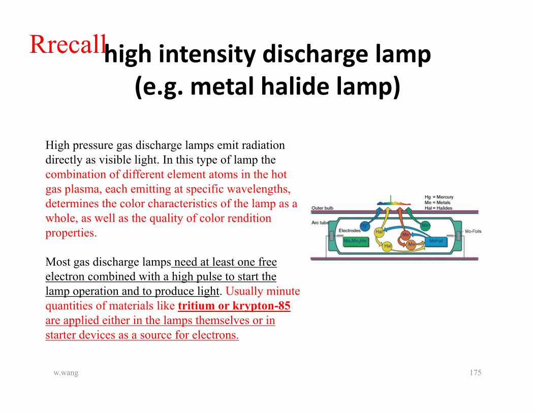
high intensity discharge lamp (e.g. metal halide lamp)
High pressure gas discharge lamps emit radiation directly as visible light. In this type of lamp the combination of different element atoms in the hot gas plasma, each emitting at specific wavelengths, determines the color characteristics of the lamp as a whole, as well as the quality of color rendition properties.
Most gas discharge lamps need at least one free electron combined with a high pulse to start the lamp operation and to produce light. Usually minute quantities of materials like tritium or krypton-85 are applied either in the lamps themselves or in starter devices as a source for electrons.
w.wang 175
Rrecall

Ion Laser
w.wang 176
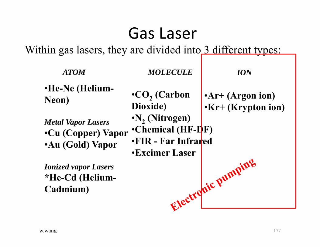
w.wang
ATOM MOLECULE ION
•He-Ne (Helium-Neon)
Metal Vapor Lasers•Cu (Copper) Vapor•Au (Gold) Vapor
Ionized vapor Lasers*He-Cd (Helium-Cadmium)
•CO2 (Carbon Dioxide)•N2 (Nitrogen)•Chemical (HF-DF)•FIR - Far Infrared•Excimer Laser
•Ar+ (Argon ion)•Kr+ (Krypton ion)
Gas Laser
177
Within gas lasers, they are divided into 3 different types:

w.wang
The Argon laser was invented in 1964 by William Bridges at Hughes. Argon ion laser contains a tube filled with Argon gas which transforms into plasma in an excited state. (Plasma is a state of matter in which the electrons are separated from the atoms and molecules, which means that it contains free electrons and ions).
Energy Level Diagram of Ion Argon Laser.
Blue 0.488 [m]
but the Argon ion laser emits also in the UV spectrum:
0.3511 [m]
0.3638 [m].
The two main laser transitions are at visible wavelengths:
green 0.5145 [m],
Argon Ion Laser
Rami Arieli: "The Laser Adventure" Chapter 6, Ion Gas Lasers, page 1178
w.wang
Krypton Laser The Krypton laser is very similar to the Argon laser, but its efficiency is lower.
This laser has many lines in the visible spectrum, especially in the yellow to red part of the spectrum.
The maximum output power in each line is about 100 [mW].
The main applications of this laser are in the art and entertainmentbusiness, to create fantastic visual effects.
179
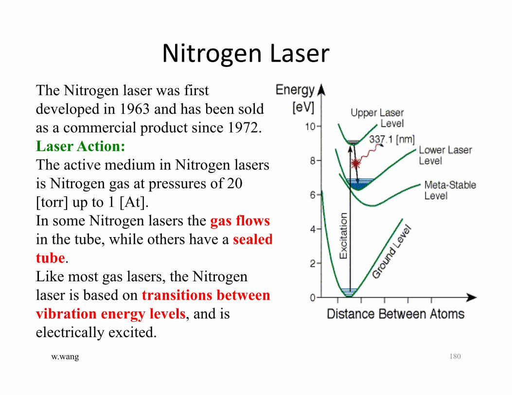
w.wang
The Nitrogen laser was first developed in 1963 and has been sold as a commercial product since 1972. Laser Action:The active medium in Nitrogen lasers is Nitrogen gas at pressures of 20 [torr] up to 1 [At]. In some Nitrogen lasers the gas flows in the tube, while others have a sealed tube. Like most gas lasers, the Nitrogen laser is based on transitions between vibration energy levels, and is electrically excited.
Nitrogen Laser
180
Molecular laser
w.wang 181

w.wang
ATOM MOLECULE ION
•He-Ne (Helium-Neon)
Metal Vapor Lasers•Cu (Copper) Vapor•Au (Gold) Vapor
Ionized vapor Lasers*He-Cd (Helium-Cadmium)
•CO2 (Carbon Dioxide)•N2 (Nitrogen)•Chemical (HF-DF)•FIR - Far Infrared•Excimer Laser
•Ar+ (Argon ion)•Kr+ (Krypton ion)
Gas Laser
182
Within gas lasers, they are divided into 3 different types:
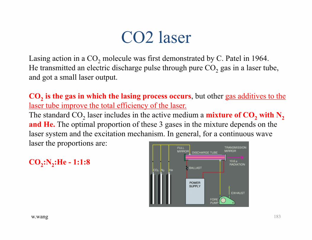
w.wang
Lasing action in a CO2 molecule was first demonstrated by C. Patel in 1964. He transmitted an electric discharge pulse through pure CO2 gas in a laser tube, and got a small laser output.
CO2 is the gas in which the lasing process occurs, but other gas additives to the laser tube improve the total efficiency of the laser. The standard CO2 laser includes in the active medium a mixture of CO2 with N2and He. The optimal proportion of these 3 gases in the mixture depends on the laser system and the excitation mechanism. In general, for a continuous wave laser the proportions are:
CO2:N2:He - 1:1:8
CO2 laser
183
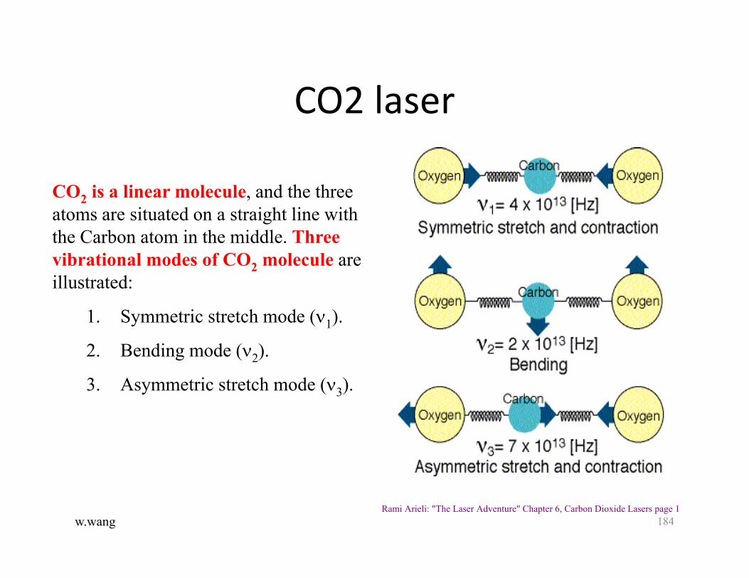
w.wang
CO2 laser
CO2 is a linear molecule, and the threeatoms are situated on a straight line withthe Carbon atom in the middle. Threevibrational modes of CO2 molecule areillustrated:
1. Symmetric stretch mode (1).
2. Bending mode (2).
3. Asymmetric stretch mode (3).
Rami Arieli: "The Laser Adventure" Chapter 6, Carbon Dioxide Lasers page 1184

w.wang
Transitions between vibrational energy states/levels results in photon emission in the infrared, while transitions between rotational states emit photons in the microwave region.
Necessary mechanisms for operation of the CO2 laser are,1. Excitation of N2 vibration by electron impact 2. Transfer of vibrational energy from N2 to the nearly resonant v3 mode of CO23. Laser transition from v3 to v1 mode.4. Sharing of population between v1 and 2v2l modes and relaxation within the v2manifold5. The vibrational energy in the v2manifold converted into translational energy by collisions with He.
CO2 laser
http://www.phy.davidson.edu/StuHome/sethvc/Laser-Final/co2.htm
185

Excimer Laser
• An excimer laser (sometimes more correctly called an exciplexlaser) is a form of ultraviolet laser which is commonly used in the production of microelectronic devices (semiconductor integrated circuits or “chips”), eye surgery, psoriasis treatment, and micromachining.
• An excimer laser typically uses a combination of a noble gas (argon, krypton, or xenon) and a reactive gas (fluorine or chlorine). Under the appropriate conditions of electrical stimulation and high pressure, a pseudo‐molecule called an excimer (or in the case of noble gas halides, exciplex) is created, which can only exist in an energized state and can give rise to laser light in the ultraviolet range.
w.wang 186

w.wang
Excimer LaserThere are lasers in which the required conditions for lasing are achieved in exotic ways. As an example, we shall examine a family of lasers in which the radiation is emitted from a molecule which only exists for a very short time. This molecule is composed of an atom of noble gas: Argon, Krypton or Xenon, and an atom of halogen: Fluorine, Chlorine, Bromine or Iodine. An Excimer is a molecule which has a bound state (existence) only in an excited state.
In the ground state this molecule does not exist, and the atoms are separated.The excited state exists for a very short time, less than 10 nanoseconds.The name Excimer comes from the combination of the two words: exited dimer, which means that the molecule is composed of two atoms, and exists only in an excited state. (Some scientists consider this molecule to be a complex, and they call the laser "Exiplex").
Excimer lasers are usually operated with a pulse repetition rate of around 100 Hz and a pulse duration of ~10 ns, although some operate at pulse repetition rates as high as 8 kHz and some have pulsewidths as large as 30 ns.
187
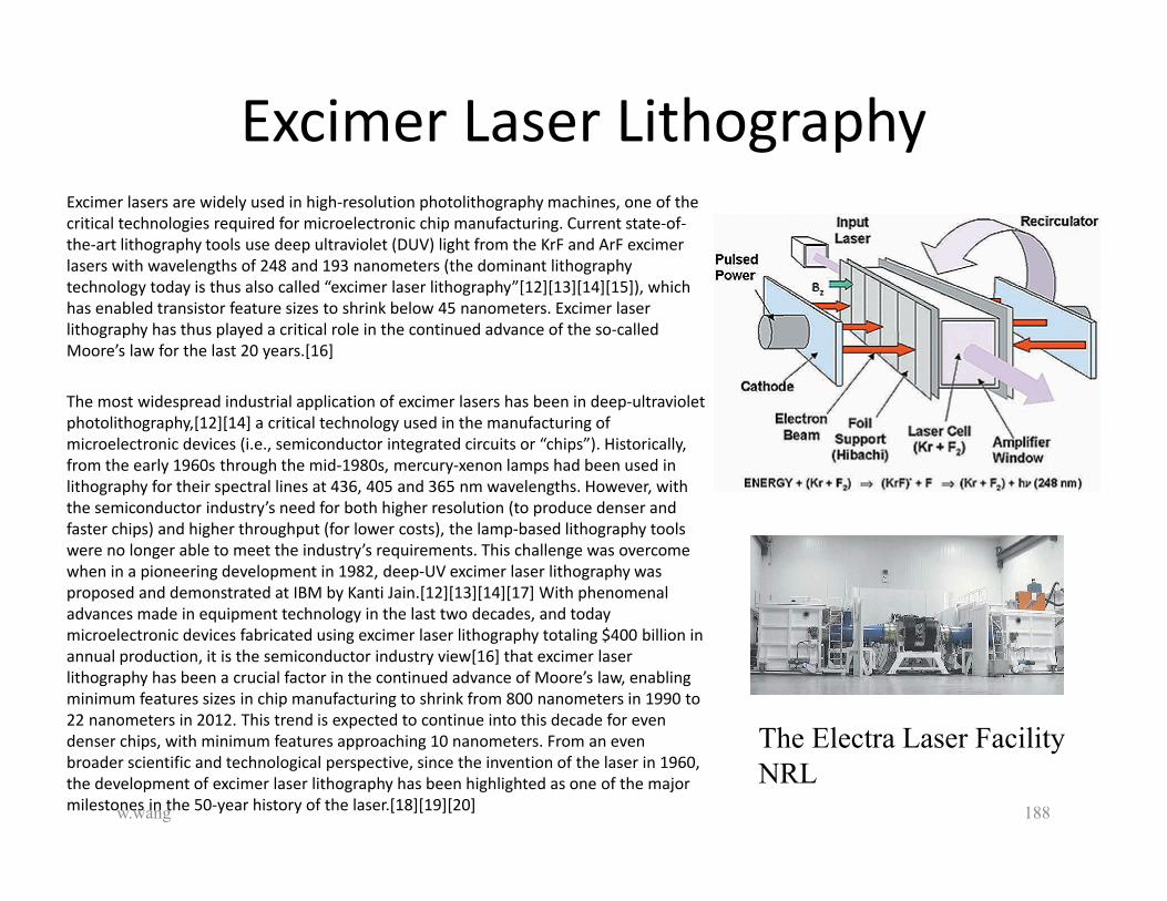
Excimer Laser LithographyExcimer lasers are widely used in high‐resolution photolithography machines, one of the critical technologies required for microelectronic chip manufacturing. Current state‐of‐the‐art lithography tools use deep ultraviolet (DUV) light from the KrF and ArF excimer lasers with wavelengths of 248 and 193 nanometers (the dominant lithography technology today is thus also called “excimer laser lithography”[12][13][14][15]), which has enabled transistor feature sizes to shrink below 45 nanometers. Excimer laser lithography has thus played a critical role in the continued advance of the so‐called Moore’s law for the last 20 years.[16]
The most widespread industrial application of excimer lasers has been in deep‐ultraviolet photolithography,[12][14] a critical technology used in the manufacturing of microelectronic devices (i.e., semiconductor integrated circuits or “chips”). Historically, from the early 1960s through the mid‐1980s, mercury‐xenon lamps had been used in lithography for their spectral lines at 436, 405 and 365 nm wavelengths. However, with the semiconductor industry’s need for both higher resolution (to produce denser and faster chips) and higher throughput (for lower costs), the lamp‐based lithography tools were no longer able to meet the industry’s requirements. This challenge was overcome when in a pioneering development in 1982, deep‐UV excimer laser lithography was proposed and demonstrated at IBM by Kanti Jain.[12][13][14][17] With phenomenal advances made in equipment technology in the last two decades, and today microelectronic devices fabricated using excimer laser lithography totaling $400 billion in annual production, it is the semiconductor industry view[16] that excimer laser lithography has been a crucial factor in the continued advance of Moore’s law, enabling minimum features sizes in chip manufacturing to shrink from 800 nanometers in 1990 to 22 nanometers in 2012. This trend is expected to continue into this decade for even denser chips, with minimum features approaching 10 nanometers. From an even broader scientific and technological perspective, since the invention of the laser in 1960, the development of excimer laser lithography has been highlighted as one of the major milestones in the 50‐year history of the laser.[18][19][20]w.wang 188
The Electra Laser FacilityNRL
Medical ApplicationThe high‐power ultraviolet output of excimer lasers also makes them useful for surgery (particularly eye surgery) and for dermatological treatment. In 1980–1983, Rangaswamy Srinivasan, Samuel Blum and James J. Wynne at IBM’s T. J. Watson Research Center observed the effect of the ultraviolet excimer laser on biological materials. Intrigued, they investigated further, finding that the laser made clean, precise cuts that would be ideal for delicate surgeries. This resulted in a fundamental patent[21] and Srinivasan, Blum and Wynne were elected to the National Inventors Hall of Fame in 2002. In 2012, the team members were honored with National Medal of Technology and Innovation by the President of The United States Barack Obama for their work related to the excimer laser.[22] Subsequent work introduced the excimer laser for use in angioplasty.[23] Xenon chloride (308 nm) excimer lasers can also treat a variety of dermatological conditions including psoriasis, vitiligo, atopic dermatitis, alopecia areata and leukoderma.
As light sources, excimer lasers are generally large in size, which is a disadvantage in their medical applications, although their sizes are rapidly decreasing with ongoing development.
w.wang 189

w.wang
Far Infra‐Red (FIR) Lasers
Far Infra-Red (FIR) lasers emit radiation in the Far-Infra-Red spectrum(wavelength range 12-1000 [m]. The wavelength range greater than 100 [m] is sometimes called sub-millimeter wave.
Far Infra-Red (FIR) lasers are gas lasers, and their lasing action occur between rotational levels of the gas molecules of the active medium. Usually these transitions are within the same vibrational level. The active medium in FIR lasers is usually a gas of simple organic molecule such as: C2H4, CF4, NH3,
Because of the very narrow width of each energy level of these materials, it is inefficient to optically pump them with ordinary light sources. The best way to achieve population inversion in these lasers is to pump them with another laser at shorter wavelength. Usually CO2 laser is used for pumping.
190

w.wang
Chemical Laser
The chemical laser is an example of a laser where the pump energy comes from a chemical reaction between two atoms. The chemical laser is a member of the family of Gas Dynamic Lasers:
Gas dynamic lasers are based on rapid expansion of hot, high pressure gas, through nozzles into a near vacuum. This rapid expansion reduce the gas temperature. As a result, since the transfer of the molecules to the ground state takes more than the time of rapid expansion, we get at low temperature many molecules at excited levels. Thus, "population inversion". The gas usually flow through the nozzles in a transverse flow(perpendicular to the optical axis of the laser), so many nozzles can operate at the same time, yielding high power from the laser.
The first chemical laser, which was operated in the pulsed mode, was developed in 1965 by J. V. V. Kasper, and G. C. Pimental. The lasing action of the chemical laser is usually based on vibrational transitions of diatomic molecule.
191
Liquid Laser
w.wang 192

w.wang
Population Inversion in lasing mediums
A. Guenther UCONN
193
- Gas (inert gas)- Liquid (pump source)- Solid state (pump source)- Semiconductor (PN junction)

FluorescenceFluorescence is a kind of luminescence, excited by irradiation of a substance with light. The light hitting a sample puts atoms, ions or molecules in the sample into excited states (by absorption of photons), from where they decay into lower‐lying states (e.g. their ground states) through spontaneous emission of fluorescence photons. This phenomenon occurs in various kinds of optically pumped lasers and amplifiers, e.g. in solid‐state doped‐insulator lasers and amplifiers (including fiber lasers and fiber amplifiers), in optically pumped semiconductor lasers, and in dye lasers. The resulting radiation is called fluorescent light.
w.wang 194
Phosphor coatingrecall

Fluorescent EmissionFirst, the energy of S1' is partiallydissipated, yielding a relaxed singletexcited state (S1) from whichfluorescence emission originates.Second, not all the molecules initiallyexcited by absorption (Stage 1) returnto the ground state (S0) by fluorescenceemission. Other processes such ascollisional quenching, fluorescenceresonance energy transfer (orintersystem crossing may alsodepopulate S1. The fluorescencequantum yield, which is the ratio of thenumber of fluorescence photonsemitted (Stage 3) to the number ofphotons absorbed (Stage 1), is ameasure of the relative extent to whichthese processes occur.
w.wang 195

w.wang
There are some molecules however, namely organic dye molecules, that do have a sufficiently long lifetime in an upper energy level (of the order of 1–5 nsec) so they can participate in the laser process by being excited to an upper laser level. These molecules also have the ability to radiate the energy from that level rather than lose the energy due to decay by collisions. Those molecules are the dyes that are used to color cloth and other objects that we use in our everyday life
When dissolved in a solvent such as alcohol or water, they can be concentrated in sufficient quantity to be used as a laser gain medium.When the light is applied to the dye solution, it is absorbed at certain wavelengths by the dye as described by absorption equation, placing the dye molecules in highly excited upper laser levels. A population inversion is then produced between those levels and a very broad range of lower-lying energy levels, thereby allowing the possibility for a wide range of laser wavelengths to be produced within the gain medium. Those lower levels are not initially pumped by the light and therefore are sufficiently empty to produce the inversion. Dye lasers thus allow the possibility of wide wavelength tunability and have been used extensively in doing a variety of spectroscopic studies in which very specific laser wavelengths are desired.
Population inversions in liquids
196
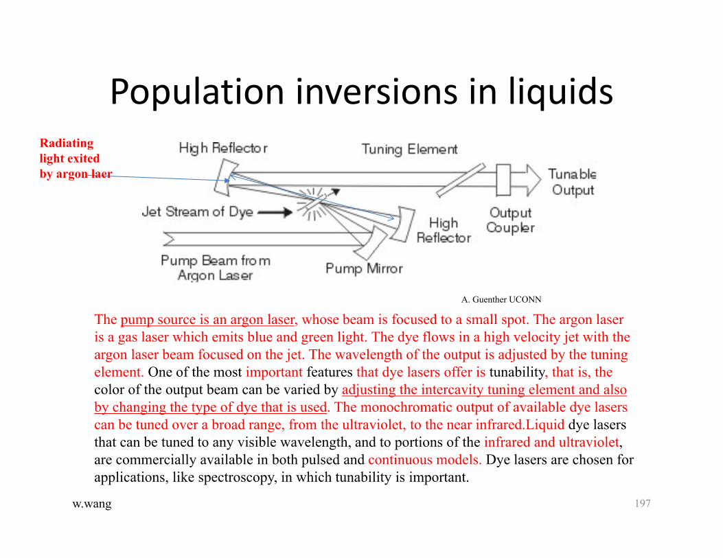
w.wang
Population inversions in liquids
The pump source is an argon laser, whose beam is focused to a small spot. The argon laser is a gas laser which emits blue and green light. The dye flows in a high velocity jet with the argon laser beam focused on the jet. The wavelength of the output is adjusted by the tuning element. One of the most important features that dye lasers offer is tunability, that is, thecolor of the output beam can be varied by adjusting the intercavity tuning element and also by changing the type of dye that is used. The monochromatic output of available dye lasers can be tuned over a broad range, from the ultraviolet, to the near infrared.Liquid dye lasers that can be tuned to any visible wavelength, and to portions of the infrared and ultraviolet, are commercially available in both pulsed and continuous models. Dye lasers are chosen for applications, like spectroscopy, in which tunability is important.
A. Guenther UCONN
197
Radiating light exited by argon laer

w.wang
A dye laser can be considered as a special device to convert electromagnetic radiation from one wavelength, to another wavelength which can be tuned. The output of a dye laser is always a coherent radiation tunable over a specific spectrum region, determined by the Dye material. A dye laser is a laser which uses an organic dye as the lasing medium, usually as a liquid solution. Molecular fluorescence is responsible for dye laser emission.
History:Dye laser was first demonstrated in 1965 at IBM laboratories in the US, by Peter P. Sorokin and J. R. Lankard. They discovered the dye laser action during a fluorescence research of organic dye molecules, which were excited by Ruby laser. In 1967 scientists discovered the possibility to tune the emitted wavelength, using a grating at the end of the optical cavity
Dye Laser
198
diagram illustrating the processes involved in the creation of an excited electronic singlet state by optical absorption and subsequent emission of fluorescence

Solid state Lasers
w.wang 199
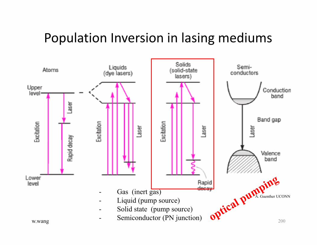
w.wang
Population Inversion in lasing mediums
A. Guenther UCONN
200
- Gas (inert gas)- Liquid (pump source)- Solid state (pump source)- Semiconductor (PN junction)

w.wang
Insulator Semiconductor
•Ruby Laser•Nd-Yag and Nd-Glass Lasers•Color Center Laser•Alexandrite Laser•Ti - Saphire Laser
•Laser Diodes
Solid State Lasers
201
A solid-state laser is a laser that uses a gain medium that is a solid, rather than a liquid such as in dye lasers or a gas as in gas lasers. Semiconductor-based lasers are also in the solid state, but are generally considered as a separate class from solid-state lasers

w.wang
Population inversions in crystalline solids and glasses
As in the case of liquids, when energy levels in solids are excited, typically by irradiating those solids with light, the levels tend to decay much more rapidly via collisions with their surrounding neighbors rather than by radiating their energy in the form of light. In a few cases, however, specific types of atoms are embedded into a transparent host material (such as a specific crystalline solid or a glass) at concentrations of up to 1 part in 100, and the atoms radiate their energy rather than decay by collisions. These specific types of atoms, such as chromium or neodymium, consist of a radiating electron surrounded by a “screen” of other electrons that protect that radiating electron from being bombarded by collisions from neighboring atoms. The consequence is that the atoms can absorb pump light that passes through the transparent host medium and can then subsequently radiate that energy. Gemstones such as rubies fall into that category. Ruby, a desired gemstone and also the material that comprised the gain medium for the first laser, consists of chromium atoms doped into a transparent sapphire (Al2O3) host crystal. The color of the ruby crystal is determined by the chromium atoms, which absorb light in the blue and green regions of the spectrum and radiate in the red. 202

w.wang
Population inversions in crystalline solids and glasses
203
Solid crystals of rare-earth salts might emit laser light if they were first irradiated with intense light of just the right wavelength, a scheme now known as optical pumping. (only in liquid or solids state laser)
Solid-state lasers include all optically pumped lasers in which the gain medium is a solid at room temperature
In solid-state laser materials, the atoms responsible for generating laser light are first excited to higher energy states through the absorption of photons, and the way in which these atoms relax from their excited states determines the quality and quantity of laser light produced .
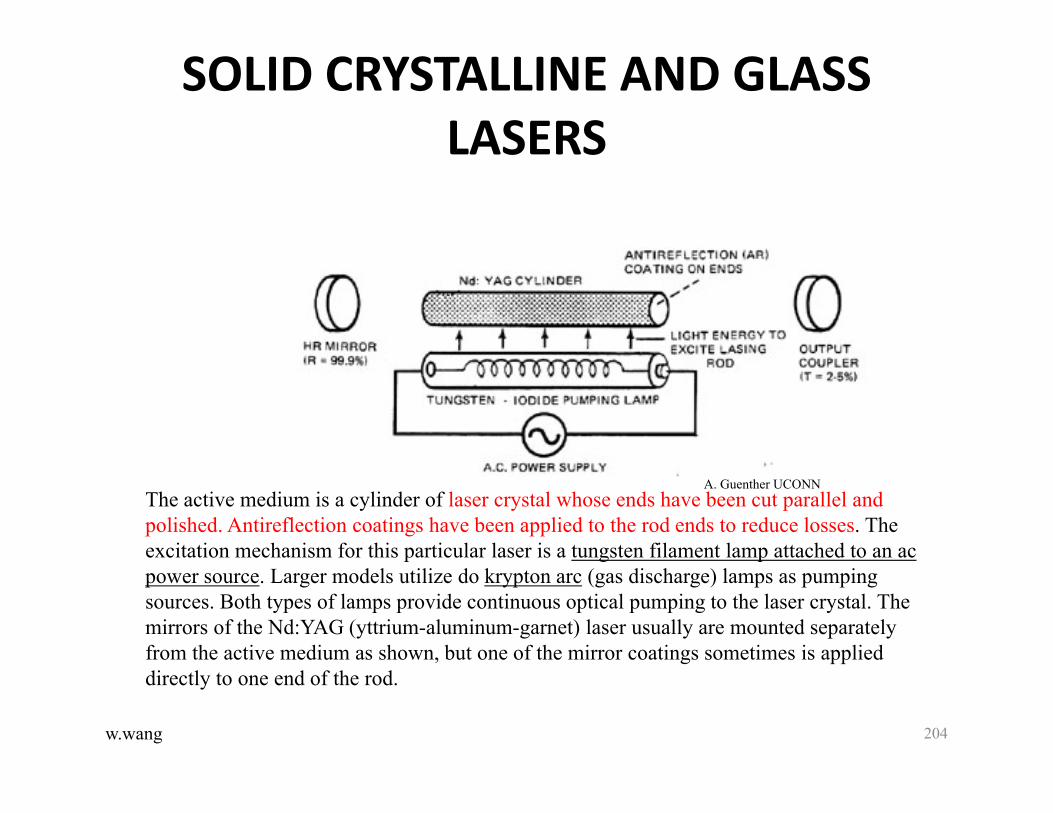
w.wang
SOLID CRYSTALLINE AND GLASS LASERS
The active medium is a cylinder of laser crystal whose ends have been cut parallel and polished. Antireflection coatings have been applied to the rod ends to reduce losses. The excitation mechanism for this particular laser is a tungsten filament lamp attached to an ac power source. Larger models utilize do krypton arc (gas discharge) lamps as pumping sources. Both types of lamps provide continuous optical pumping to the laser crystal. The mirrors of the Nd:YAG (yttrium-aluminum-garnet) laser usually are mounted separately from the active medium as shown, but one of the mirror coatings sometimes is applied directly to one end of the rod.
A. Guenther UCONN
204

w.wang
Pump Sources
A. Guenther UCONN
Pumping lasers include the argon ion or doubled Nd:YAG cw lasers for pumping titanium-sapphire lasers, excimer lasers for pumping dye lasers, and gallium arsenide semiconductor lasers for pumping Nd:YAG lasers.
The most common types of flashlamps used for pumping lasers are narrow, cylindrical quartz tubes with metal electrodes mounted on the ends, filled with a gaseous species such as xenon that serves as the radiating material within the lamp.Xenon is the most common species because of both its radiating efficiency and its emission of a broad spectrum of wavelengths from which to choose in matching the lamp emission to the pumping absorption bands of the laser.
205

w.wang
Ruby laser was the first man made laser, which was build by Theodore Maiman in 1960. Ruby is a synthetic crystal of Aluminum Oxide (Al2O3), and is more familiar in daily life as a precious stone for jewel. The chemical structure of Ruby is of Al2O3 (which is called Sapphire), with impurity of about 0.05% (by weight) of Chromium Ions (Cr+3). The active ion is Cr+3, which replace Al atom in the crystal. This ion causes the red color of the crystal. The impurity ion of Cr+3 is responsible for the energy levels which participate in the process of lasing.
Ruby Laser
206
w.wang
Nd LaserIn Nd laser Nd+3 ions (as impurities of up to a few percent by weight) are replacing the atoms of the solid host in the active medium.
Three known solid hosts are used for Nd-YAG laser where Nd+3 ions are added as impurities: •Glass. •YAG (Yttrium Aluminum Garnet) Crystal. •YLF (LiYF4) Crystal.
The choice between the three possible hosts is according to the intended use of the laser: •Glass is used as the host material when a pulsed laser is needed, with each pulse at high power, and the pulse repetition rate is slow. The active medium of Nd-Glass Laser can be manufactured in a shape of disk or rod, with diameters of up to 0.5 meter (!) and length of up to several meters (!). Such dimensions are possible because glass is isotropic material, cheap, and can be easily worked to the right shape. High percentage (up to about 6%) of Nd ions can be added to glass as impurity. The problem with glass as a host is its poor thermal conductivity. Thus cooling the laser when it operates continuously or at high repetition rate is difficult. •YAG crystal is used for high repetition rate pulses (more than one pulse per second). In this case a large amount of heat need to be transferred away from the laser, and the thermal conductivity of the YAG crystal is much higher than that of glass.•YAG crystal with the high quality needed for lasers can be made with diameters of 2-15 [mm] and at lengths of 2-30 [cm]. •The price of a YAG laser rod is high, since growing crystals is a slow and complicated process. •The percentage of Nd ions in the YAG host is 1-4% by weight. 207

w.wang
Laser gain bandwidths for the HeNe, Nd:YAG, and Ti:Al2O3 lasers
Bandwidth of laser gain medium
The bandwidth of the laser gain medium determines the range of wavelengths over which amplification can occur for any specific laser. This bandwidth is expressed in either a wavelength range G or a frequency range vG. These two expressions are related by
in which is the laser wavelength and c is the speed of light. The bandwidth of the gain medium is usually determined by the bandwidth over which the spontaneous emission occurs for a given laser transition.
A. Guenther UCONN
208
Full width at half maximum (FWHM)
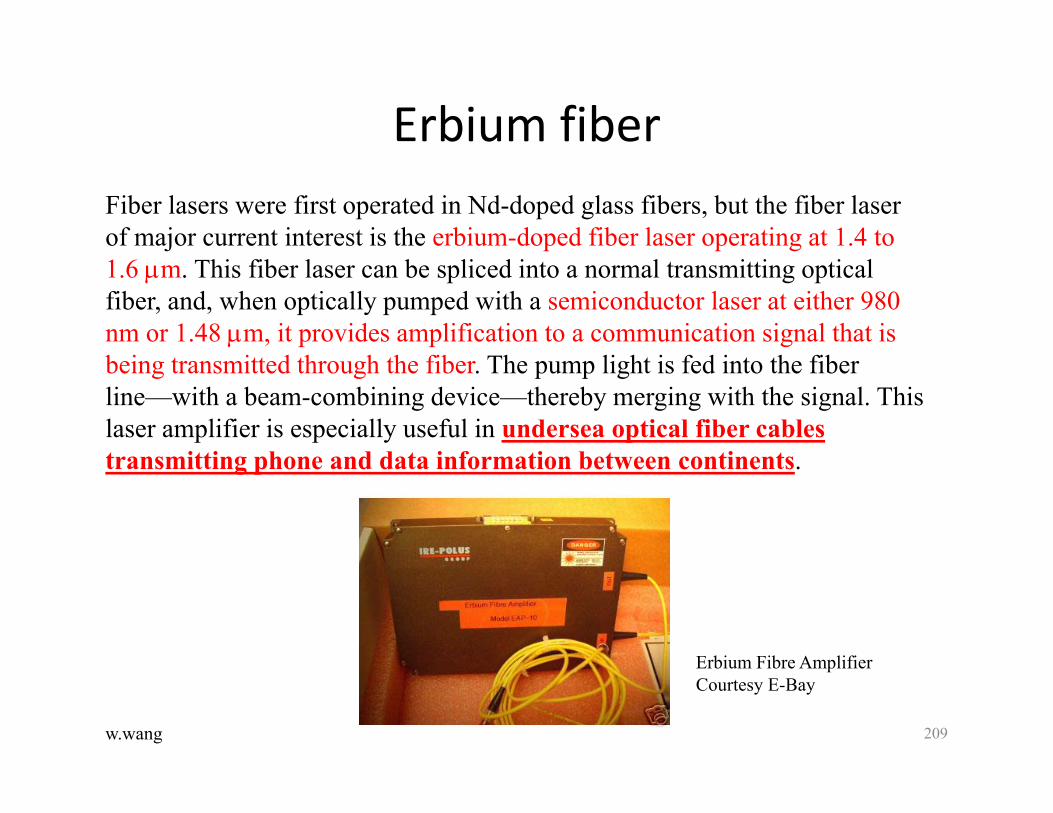
w.wang
Fiber lasers were first operated in Nd-doped glass fibers, but the fiber laser of major current interest is the erbium-doped fiber laser operating at 1.4 to 1.6 m. This fiber laser can be spliced into a normal transmitting optical fiber, and, when optically pumped with a semiconductor laser at either 980 nm or 1.48 m, it provides amplification to a communication signal that is being transmitted through the fiber. The pump light is fed into the fiber line—with a beam-combining device—thereby merging with the signal. This laser amplifier is especially useful in undersea optical fiber cables transmitting phone and data information between continents.
Erbium fiber
Erbium Fibre AmplifierCourtesy E-Bay
209

Semiconductor Lasers
w.wang 210

w.wang
Population Inversion in lasing mediums
A. Guenther UCONN
211
- Gas (inert gas)- Liquid (pump source)- Solid state (pump source)- Semiconductor (PN junction)
w.wang
Semiconductor lasers are quite different from conventional lasers. In particular:
1. The gain of the laser material is very high and is generated by a population inversion between the conduction and valence bands of semiconductors. In some sense, a semiconductor laser is a two-state laser system.
2. Since the electromagnetic mode is on the order of the size of the laser device, then the transverse mode of the semiconductor laser is quite different from that of a conventional laser. In particular, the beam is not Gaussian, the beam profile tends to be elliptical, and the beam divergence tend to be large.
3. The gain spectrum is quite large (many THz or hundreds of angstroms). 4. The short cavity (several hundred microns) means that the longitudinal
mode spacing is much larger than that of a conventional gas or solid state laser (on the order of GHz or angstroms).
Semiconductor Lasers
212

w.wang
Laser gain bandwidths for the HeNe, Nd:YAG, and Ti:Al2O3 lasers
Bandwidth of laser gain medium
The bandwidth of the laser gain medium determines the range of wavelengths over which amplification can occur for any specific laser. This bandwidth is expressed in either a wavelength range G or a frequency range vG. These two expressions are related by
in which is the laser wavelength and c is the speed of light. The bandwidth of the gain medium is usually determined by the bandwidth over which the spontaneous emission occurs for a given laser transition.
A. Guenther UCONN
213
Full width at half maximum (FWHM)
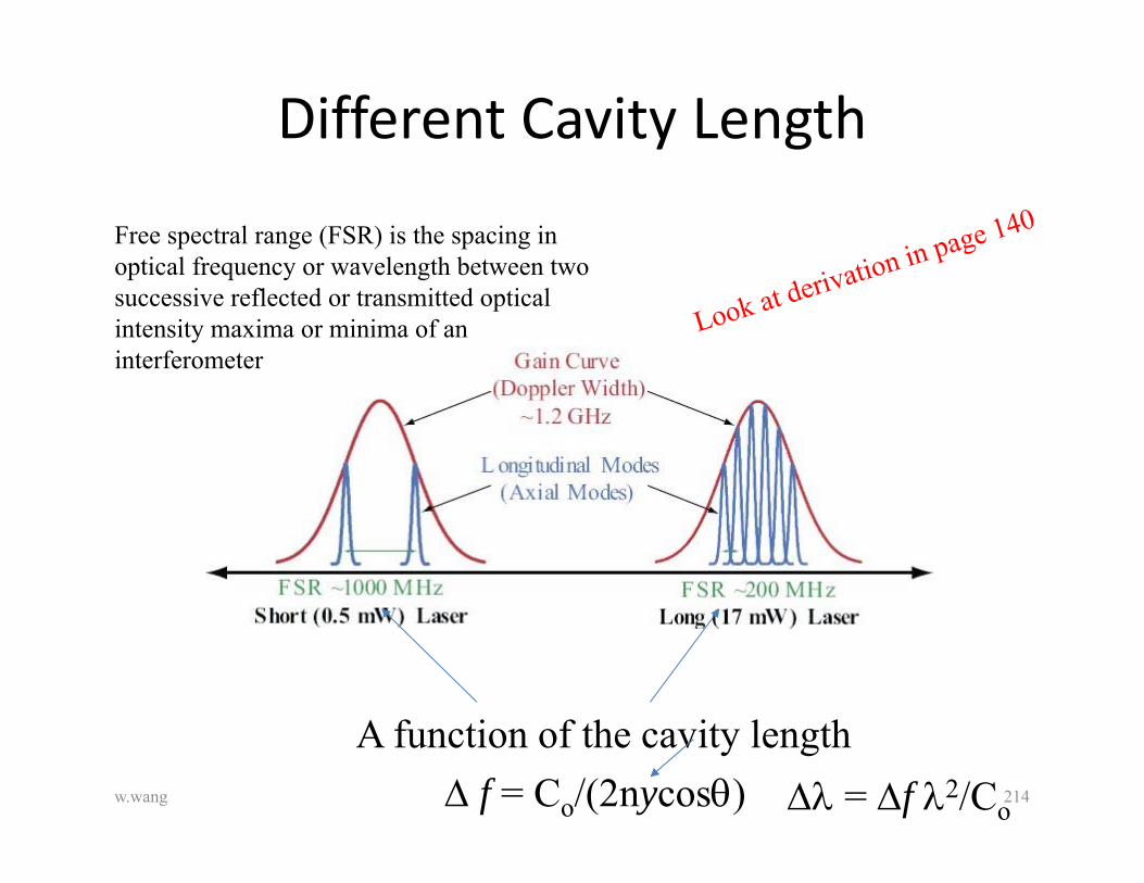
Different Cavity Length
w.wang 214
A function of the cavity lengthf = Co/(2nycos)
Free spectral range (FSR) is the spacing in optical frequency or wavelength between two successive reflected or transmitted optical intensity maxima or minima of an interferometer
= f 2/Co
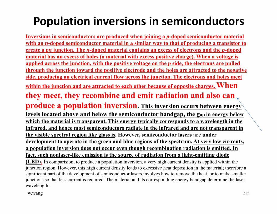
w.wang
Population inversions in semiconductorsInversions in semiconductors are produced when joining a p-doped semiconductor material with an n-doped semiconductor material in a similar way to that of producing a transistor to create a pn junction. The n-doped material contains an excess of electrons and the p-doped material has an excess of holes (a material with excess positive charge). When a voltage is applied across the junction, with the positive voltage on the p side, the electrons are pulled through the junction toward the positive electrode and the holes are attracted to the negative side, producing an electrical current flow across the junction. The electrons and holes meet
within the junction and are attracted to each other because of opposite charges. When they meet, they recombine and emit radiation and also can produce a population inversion. This inversion occurs between energy levels located above and below the semiconductor bandgap, the gap in energy below which the material is transparent. This energy typically corresponds to a wavelength in the infrared, and hence most semiconductors radiate in the infrared and are not transparent in the visible spectral region like glass is. However, semiconductor lasers are under development to operate in the green and blue regions of the spectrum. At very low currents, a population inversion does not occur even though recombination radiation is emitted. In fact, such nonlaser-like emission is the source of radiation from a light-emitting diode (LED). In comparision, to produce a population inversion, a very high current density is applied within the junction region. However, this high current density leads to excessive heat deposition in the material; therefore a significant part of the development of semiconductor lasers involves how to remove the heat, or to make smaller junctions so that less current is required. The material and its corresponding energy bandgap determine the laser wavelength.
215
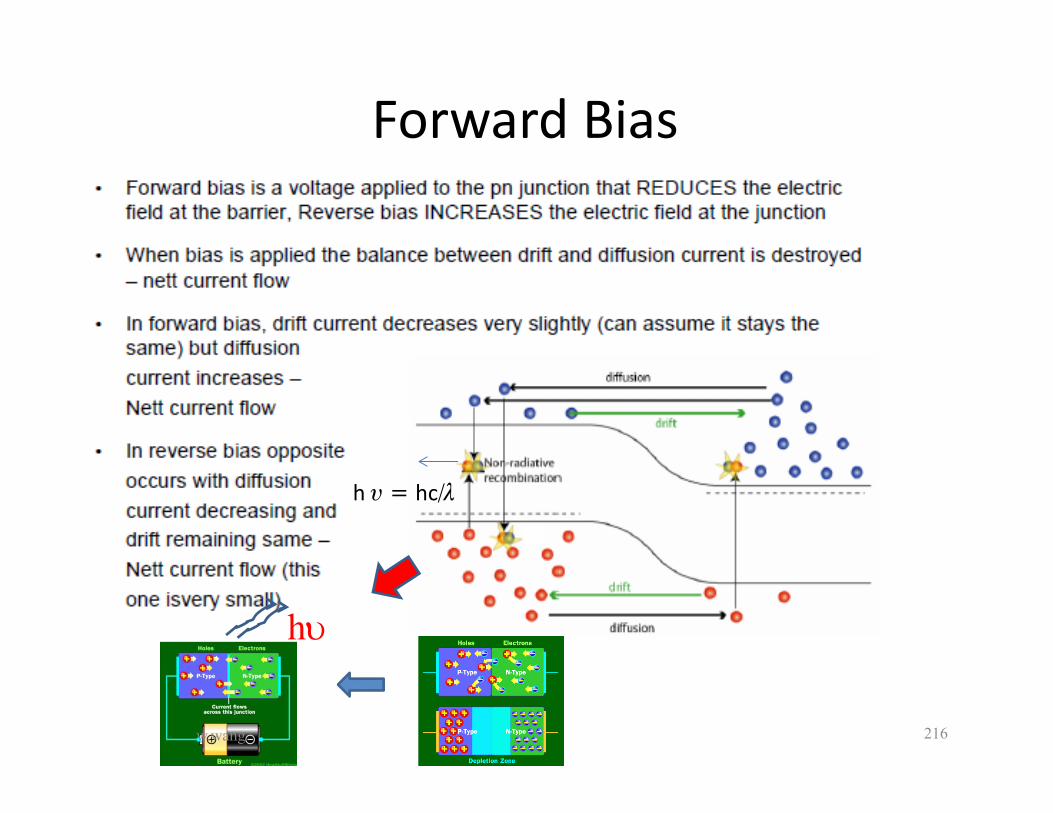
Forward Bias
h hc
w.wang 216
h

w.wang
Band structure near a semiconductor p-n junction. Left: No forward-bias voltage. Right: Forward-bias voltage present
Semiconductor Lasers
217
shows the relative populations of the energy bands or both sides of a p-n junction with no voltage applied to the diode. The n-type material contains electrons which behave as the current carriers in its conduction band, whereas the p-type material has holes for carriers in its valence band. When a forward voltage is applied to the diode, the energy levels are caused to shift. Under these conditions there is a significant increase in the concentration of electrons in the conduction band near the junction on the n-side and the concentration of holes in the valence band near the junction on the p-side.
The electrons and holes recombine and energy is given off in the form of photons. The energy of the photon resulting from this recombination is equal to that associated with the energy gap. In light-emitting diodes (LED) this light energy is transmitted out through the sides of the junction region. For the LED, all of the light is created by spontaneous emission due to electron and hole recombination. In semiconductor lasers the junction forms the active medium, and the reflective ends of the laser material provide feedback. Because of this feedback in diode lasers, most of the light is created by stimulated emission.

w.wang
Semiconductor Lasers
Semiconductor lasers are light-emitting diodes within a resonator cavity that is formed either on the surfaces of the diode or externally. An electric current passing through the diode produces light emission when electrons and holes recombine at the p-n junction. Because of the small size of the active medium, the laser output is very divergent and requires special optics to produce a good beam shape. These lasers are used in optical-fiber communications, CD players, and in high-resolution molecular spectroscopy in the near-infrared. Diode laser arrays can replace flashlamps to efficiently pump solid-state lasers.Diode lasers are tunable over a narrow range and different semiconductor materials are used to make lasers at 680, 800, 1300, and 1500 nm.
218
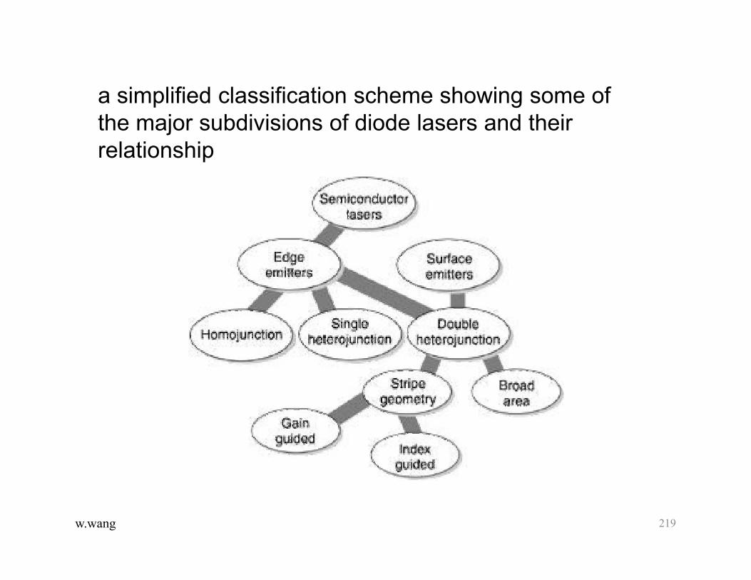
w.wang
a simplified classification scheme showing some of the major subdivisions of diode lasers and their relationship
219

w.wang
Simplest (and earliest) type of gallium arsenide laser(Edge Emission)
220

w.wang
Structure and index of refraction for various types of junction in the aluminum gallium arsenide system.
Top: Homojunction.
Middle: Single heterojunction.
Bottom: Double heterojunction
221
The variation in doping provided a small step in the index of refraction, as indicated on the right side of the figure. This tended to provide some confinement of light in the region of the junction, because of total internal reflection.
Homojunction and Heterojunction
Energy levels at a heterojuctionallow conduction electronics to drop to the low band gap side, but not t return to the high-band gap side

w.wang
Modern diode lasers are formed of structures that contain several thin layers of material of varying composition.
222
Double Heterostructure( edge emission)

w.wang
Amplification
A semiconductor laser amplifier is a forward bias heavily doped p-n junction fabricatedFrom a direct gap semiconductor materials. The injected current is sufficiently largeTo provide optical gain. The gain coefficient ro(v) of the laser amplifier has a peak value rp that is approximately proportional to the injected carrier concentration, whichIn turn, proportional to the injected current density J
rp ~(J/Jt –1), Jt= nTel/intr
Where r = electron-hole recombination lifetimein= /r is the internal quantum efficiencyl = thickness of the active region = thermal equilibrium absorption coefficientnT and Jt are injected-carrier concentration and current density just to make the semiconductor transparent.
P nl
w
d i
Cleave surface
223

w.wang
Feedback
The feedback is usually obtained by cleaving the crystal planes normal to thePlane of the junction, or by polishing two parallel surfaces of the crystal.The active region serves as a planar-mirror optical resonator of length dand cross-sectional area lw. The reflectance at theSemiconductor-air interface is
R = (n-1/n+1)2
For GaAs, n=3.6 and R=0.32 P nl
w
d i
Cleave surface
224

w.wang
Resonator Losses
The principle source of resonator loss arises from the partial reflection at the surfaces of the crystal. For a resonator of length d the reflection loss coefficient is
m = m1 +m2 = (1/2d)ln(1/R1R2)
If two surfaces have the same reflectance R1=R2 =R, then am= (1/d)ln(1/R).
Include confinement factor which represents the fraction of the optical Energy lying within the active region (l), the total loss
r = 1/ (s +m)
Where s represents other sources of loss including free carrier absorption in and scattering from optical inhomogeneities.
225

w.wang
Gain Condition: Laser threshold
The laser oscillation condition is the gain exceed the loss, rp > r, as discussed in the earlier section. The threshold gain coefficient is thereforer. Set J = Jt and rp= ar, the threshold injected current density Jt is
Jt = JT(r + )/ or I = JA
Where the transparency current density,
JT = elnT/(r) or iT = J T A; A = wd
Smaller Jt indicates superior performance, maximize and minimize r, minimize transparent injected-carrier concentrationnT and l. however, l is reduced beyonda point ther, increases because the confinement factor
226

w.wang
Gain Condition (Laser Threshold)
Double heterostructure
homostructure
l
Jt
The confinement factor remains near 1 forlower values l becausethe active layer behaves as an optical waveguideThe result is a lower Jt
227

w.wang
Internal Photon Flux
When laser current density is increased above its threshold value (J > Jt), the amplifier peak gain p exceeds loss coefficient r. Stimulated emission then outweights absorption and otherResonator losses so oscillation begin and the photon flux increases
int i-it)/e , i > it (steady-state laser internal photon flux)= 0 , i < it
Photons per second generated within the active region
The internal laser power above threshold is simply related to the internal photon flux by P=hv So we have
P = 1.24 int i-it)/o
228

w.wang
Output Flux and Efficiency
The output flux is the product of internal flux and emission efficiency , which is the ratio of the loss associated with the useful light transmitted through the mirrors to the total resonator loss e = m / r = m1 +m2 = [(1/2d)ln(1/R1R2)]/
eint i-it)/e
The laser output power above threshold is
Pout = 1.24d i-it)/o , d = ein (differential quantum efficiency)
i
Pout
it
Slope = dPout/di = 1.24d/o(differential responsivity)
229

w.wang
Output Characteristics
At low values of the input, the device acts as a light-emitting diode (LED), producing a relatively small amount of incoherent light.
At a threshold value, where the population inversion is large enough so that gain by stimulated emission can overcome the losses, the laser threshold is reached. As current increases above the threshold value, the light output increases much more rapidly than in the LED region. 230

w.wang
Overall Efficiency
The overall efficiency (Power-conversion efficiency) is defined as the ratio of the emitted laser light power to the power to the electrical input power iV
d (1-(it/I))hv/eV
231

w.wang
Temperature Dependence of Laser Output
a) Schematic sketch of the output of a typical laser diode as a function of drive current for three different operating temperatures. b) Temperature dependence of threshold current.
232

w.wang
Gallium arsenide lasers emit radiation in the near infrared portion of the spectrum. The exact wavelength depends on the temperature at which the laser is operated.
Wavelength as a function of Temperature
233
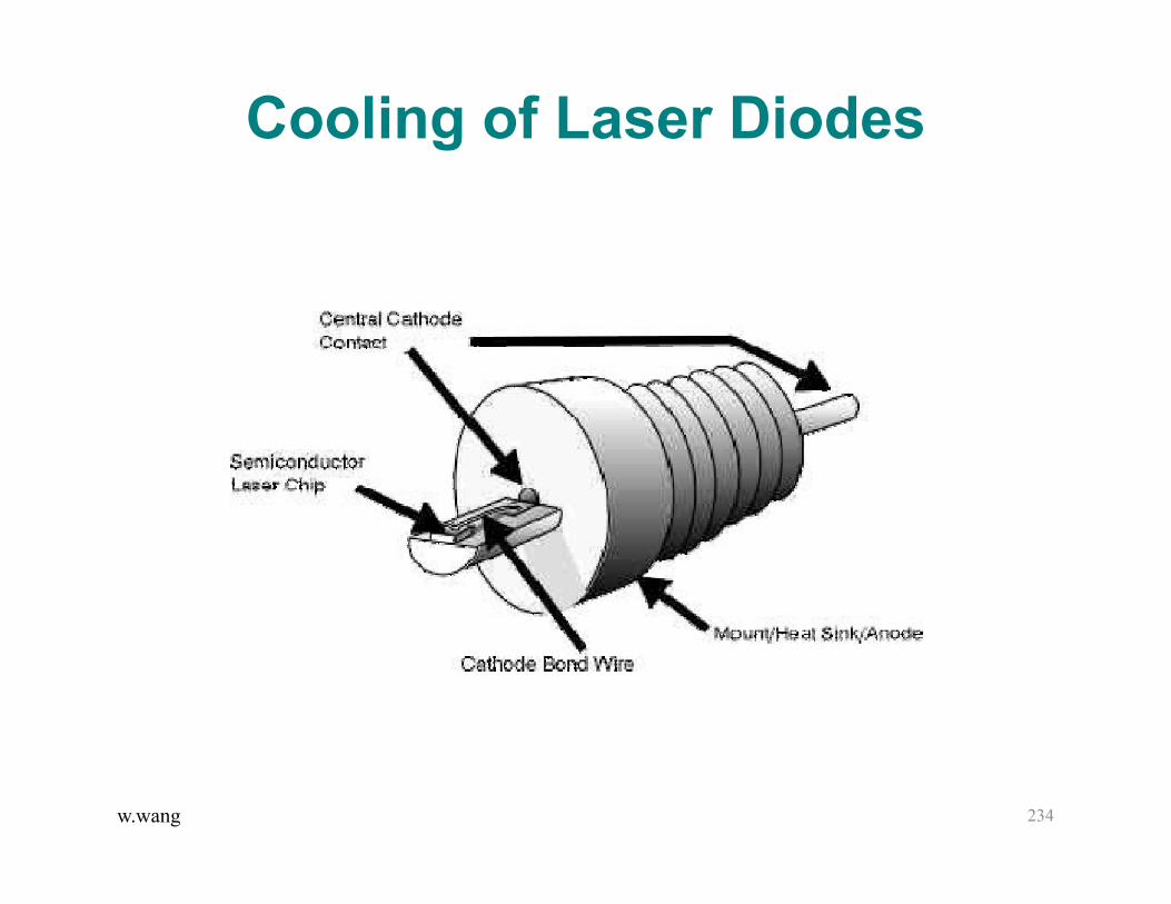
w.wang
Cooling of Laser Diodes
234

w.wang
Infineon Technologies, Agilent Technologies, Hitachi, Intelite, Laser Components Instrument Group, Alcatel, Furukawa Electrics, Mitshubishi
235

w.wang
Spectral Characteristics
The spectral distribution is governed by three factors
1. Spectral width B within which the active medium small signal gain is greater the loss coefficient r
2. Homogeneous and inhomogeneous nature of the line-broadening mechanism
3. Resonant modes vf = C / 2nd
236
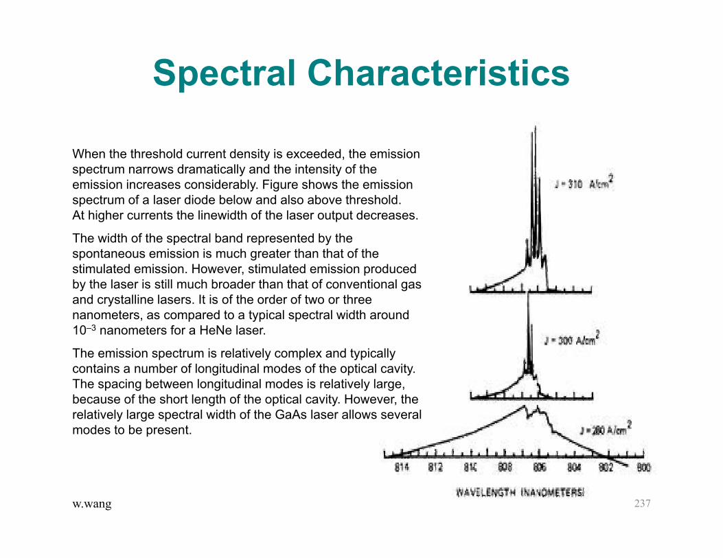
w.wang
Spectral Characteristics
When the threshold current density is exceeded, the emission spectrum narrows dramatically and the intensity of the emission increases considerably. Figure shows the emission spectrum of a laser diode below and also above threshold. At higher currents the linewidth of the laser output decreases.
The width of the spectral band represented by the spontaneous emission is much greater than that of the stimulated emission. However, stimulated emission produced by the laser is still much broader than that of conventional gas and crystalline lasers. It is of the order of two or three nanometers, as compared to a typical spectral width around 10–3 nanometers for a HeNe laser.
The emission spectrum is relatively complex and typically contains a number of longitudinal modes of the optical cavity. The spacing between longitudinal modes is relatively large, because of the short length of the optical cavity. However, the relatively large spectral width of the GaAs laser allows several modes to be present.
237

w.wang
Far‐Field Radiation Pattern
P nl
w
d i
Cleave surface
o/l
o/wA laser diode with an active dimnesion l and w emitsLight with far field angular divergence ~ o/l in the Plane perpendicular to the junction and o/w in thePlane parallel to the junction.
Assume Gassian beam of diameter 2Wo, the divergence angle is W
Active layer
238

w.wang
Spatial Characteristics
A semiconductor laser typically has an elliptical spatial profile
The profile is caused by diffraction. Light is emitted through the aperture defined by the small junction. Diffraction through the narrow dimensions of the junction causes the beam to spread into a broader angle than is observed with other types of lasers.
239

w.wang
Laser Lifetime
Two different types of failure mechanisms have been identified in gallium arsenide lasers. One is a catastrophic decrease in the power output. This catastrophic damage may occur within a single pulse of the laser, and it is associated with damage of the end surfaces of the laser. The damage is produced by the light output of the laser itself. Tiny cracks or grooves in the junction are produced. To avoid this type of damage, peak power output of the laser must be limited.
There is also a gradual increase in power, which is manifested by increasing threshold current. This damage is produced by the current flowing through the junction. This is a complex phenomenon that is complicated by random variations in the laser life. To extend the life of the laser diode, current density through the junction should be limited.
240

w.wang
Other Types of Semiconductor Lasers
Material Wavelength (µm)Material Wavelength (µm)ZnS ZnOGanZnSeCdSZnTeGaSeCdSeCdTe
0.33 0.370.400.460.490.530.590.6750.785
GaAsInP
GaSbInAsTe
PbSInSbPbTePbSe
0.84-0.950.911.553.13.724.35.26.58.5
241

w.wangWavelength ranges covered by a number of semiconductor lasers of mixed composition
242

w.wang
Distributed‐feedback (DFB) laser
With introduction of a corrugated structure into the cavity of the laser, only light of a very specific wavelength is diffracted and allowed to oscillate.
243

w.wang
14-pin DIL package (Courtesy of Lasertron)
1550-nm DFB laser in butterfly package (Courtesy of Lasertron)
Packaging
244

w.wang
Laser fiber coupling
245

Laser Applications
w.wang 246

w.wang
Laser applications
Industrial applications:engraving, cutting, scribing, drilling, tooling, welding, etc.
Medical applications: cutting, soldering, correct visiondiagnostics of cancer cells using fluorescence, and photo dynamic therapy , remove unwanted tissue, photothermal, etc.
Micromachining: 3-D micromaching, etching, engraving, etc.
247
w.wang"Laser Applications and Processing in Precision Manufacturing" was help at the EOC on December 7, 2000
248
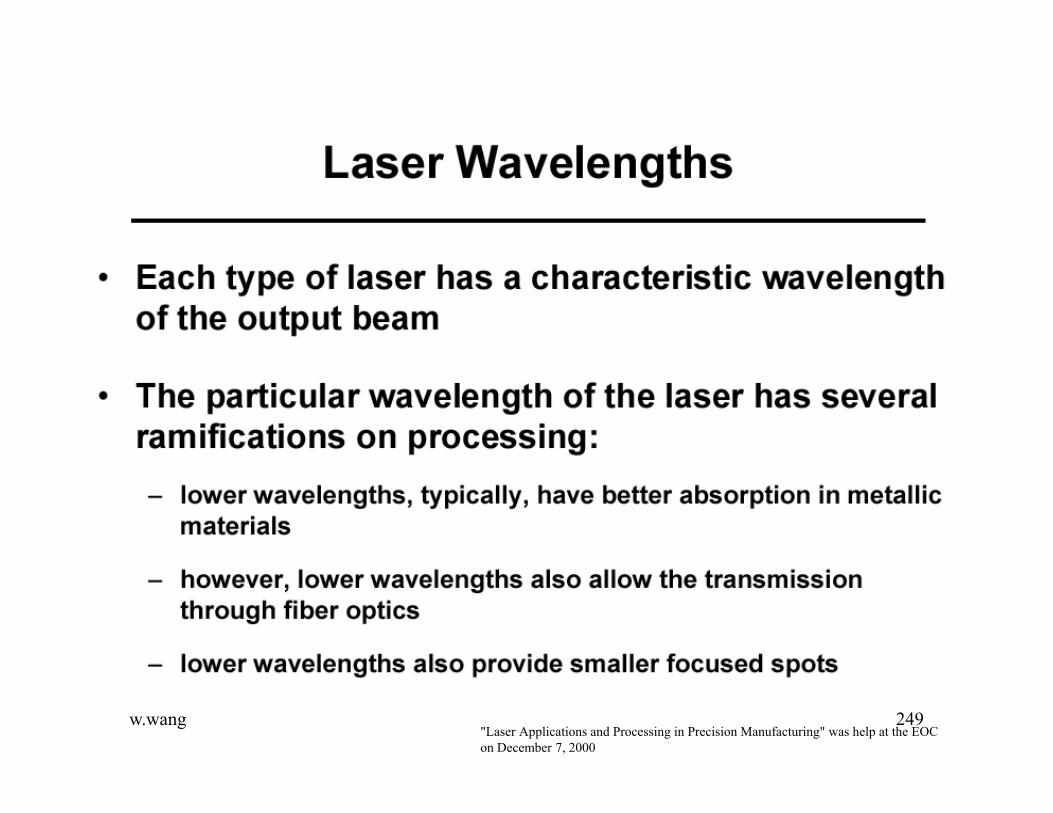
w.wang"Laser Applications and Processing in Precision Manufacturing" was help at the EOC on December 7, 2000
249
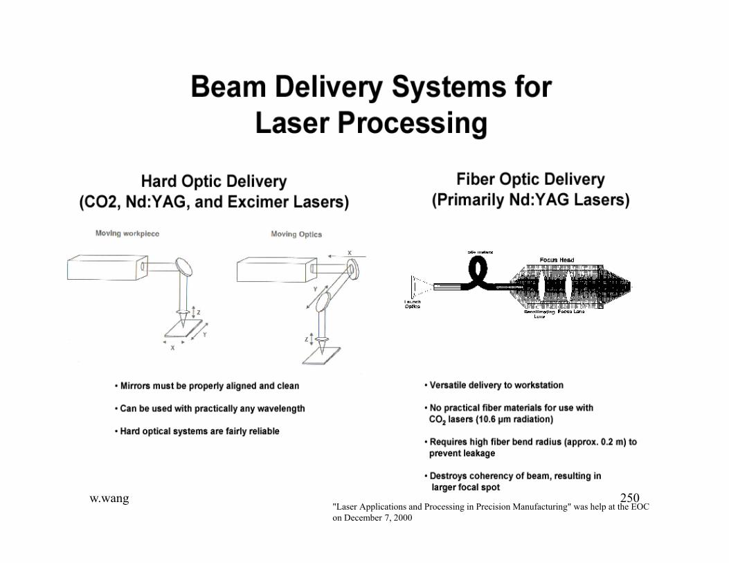
w.wang"Laser Applications and Processing in Precision Manufacturing" was help at the EOC on December 7, 2000
250

w.wang
There are major performance differences between Nd:YAG and CO2 lasers. One reason is that Nd:YAG light is emitted at a wavelength of 1.06 microns in the near infrared, while CO2 light is emitted at 10.6 microns. The material interactions at these wavelengths differ. Most organics don't absorb 1 micron light very well, while they absorb 10 micron light. So, non-metal processing is generally a CO2 application. Metals are more reflective at 10 microns than at 1 micron, so CO2 lasers only weld effectively in the "keyhole" mode, where the irradiance is high enough to generate a vapor channel in the workpiece. Once you get into keyhole mode, the high average power of CO2 lasers makes high speed welding possible. For small spot welds, Nd:YAG lasers are far more controllable.
Also, since there are a lot more Nd atoms in a YAG rod than there are CO2 atoms in laser gas, Nd:YAG lasers can deliver much higher peak powers than CO2 lasers. This makes them better for drilling. Conversely, since it's hard to cool a solid rod, Nd:YAG lasers have problems with high average powers. You can build a CO2 laser with very high power; Convergent has commercial 45 kW units, and much bigger ones have been built.
251

w.wang"Laser Applications and Processing in Precision Manufacturing" was help at the EOC on December 7, 2000
252

w.wang 253

w.wang"Laser Applications and Processing in Precision Manufacturing" was help at the EOC on December 7, 2000
254

w.wang"Laser Applications and Processing in Precision Manufacturing" was help at the EOC on December 7, 2000
255

w.wang
Lasers in General Surgery
Almost every medical surgery in which a removal of tissue is required, or a cut needs to be made, can be done with a laser. In general, the results using lasers are better than the results using a surgical knife.
•When a bleeding need to be stopped, a Nd-YAG laser can be used. Its radiation enters deep into the tissue, and heats and coagulates a large area. •When a clean cut need to be done, an Excimer laser is used. •A more general cutting tool is the CO2 laser.
256

w.wang
Dental soft tissue treatment applications are similar to those of other soft tissue in the body, and are common for many years.
•In case of gum surgery, with the laser most of the patients suffer less postoperative pain. •Almost no bleeding. •No stitches required.
Dental hard tissue treatment is new, and only in May 1997 the FDA (Federal Drug Administration) approved the Er-YAG laser for use on the hard tissue (teeth) in humans.
Lasers in Dentistry
Rami Arieli: "The Laser Adventure" Chapter 9.2.1 page 11
257
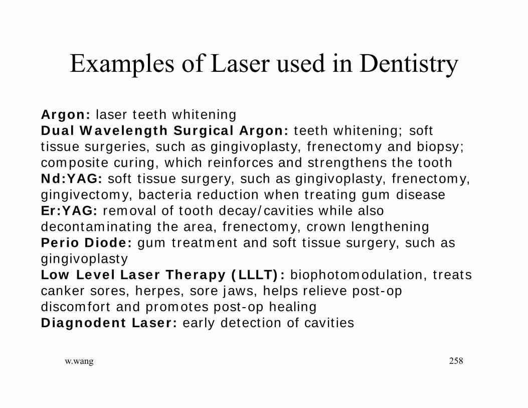
w.wang
Argon: laser teeth whitening Dual Wavelength Surgical Argon: teeth whitening; soft tissue surgeries, such as gingivoplasty, frenectomy and biopsy; composite curing, which reinforces and strengthens the tooth Nd:YAG: soft tissue surgery, such as gingivoplasty, frenectomy, gingivectomy, bacteria reduction when treating gum disease Er:YAG: removal of tooth decay/cavities while also decontaminating the area, frenectomy, crown lengthening Perio Diode: gum treatment and soft tissue surgery, such as gingivoplasty Low Level Laser Therapy (LLLT): biophotomodulation, treats canker sores, herpes, sore jaws, helps relieve post-op discomfort and promotes post-op healing Diagnodent Laser: early detection of cavities
Examples of Laser used in Dentistry
258
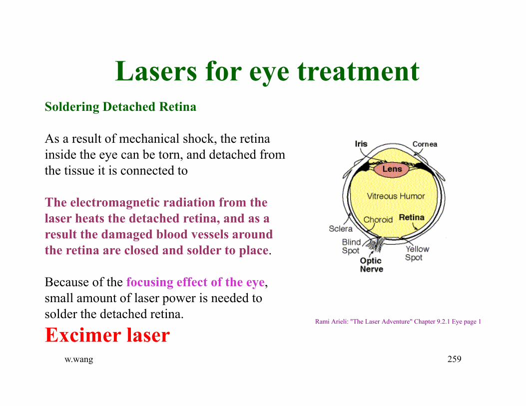
w.wang
Soldering Detached Retina
As a result of mechanical shock, the retina inside the eye can be torn, and detached from the tissue it is connected to
The electromagnetic radiation from the laser heats the detached retina, and as a result the damaged blood vessels around the retina are closed and solder to place.
Because of the focusing effect of the eye, small amount of laser power is needed to solder the detached retina.
Excimer laser
Lasers for eye treatment
Rami Arieli: "The Laser Adventure" Chapter 9.2.1 Eye page 1
259
w.wang Rami Arieli: "The Laser Adventure" Chapter 9.2.2 page 1
Lasers in Diagnostic Medicine, and in combination with Drugs
Diagnostics of cancer cells using Fluorescence, and Photo Dynamic Therapy (PDT)
One of the biggest problems in medicine today is to find a cure for cancer.
There are many treatments for cancer to destroy the cancer cells, such as:
• Disectomy of the infected organ. • Radioactive irradiation. • Heat treatment.
260
w.wang
Types of LasersAlthough there are several different kinds of lasers, only three kinds have gained wide use in medicine: Carbon dioxide (CO2) laser—This type of laser can remove thin layers from the skin's surface without penetrating the deeper layers. This technique is particularly useful in treating tumors that have not spread deep into the skin and certain precancerous conditions. As an alternative to traditional scalpel surgery, the CO2 laser is also able to cut the skin. The laser is used in this way to remove skin cancers. Neodymium:yttrium-aluminum-garnet (Nd:YAG) laser—Light from this laser can penetrate deeper into tissue than light from the other types of lasers, and it can cause blood to clot quickly. It can be carried through optical fibers to less accessible parts of the body. This type of laser is sometimes used to treat throat cancers. Argon laser—This laser can pass through only superficial layers of tissue and is therefore useful in dermatology and in eye surgery. It also is used with light-sensitive dyes to treat tumors in a procedure known as photodynamic therapy (PDT).
261

w.wang
Soft lasers
Rami Arieli: "The Laser Adventure" Chapter 9.2.3 page 1
Most of the medical laser applications were until recently based on the thermal effects caused by the electromagnetic radiation which was absorbed in the biological tissue.
In the last few years, some new applications are using low power lasers with output power less than 1 Watt.
Some of the effects of these low power levels on the biological tissue is not thermal, and in effect the mechanism of interaction is not yet clear.
It is sometimes referred to as Biostimulation, which does not explain a lot.
262

w.wang
Lasers in Dermatology
Among these defects are: •Pigmented skin, Abnormal skin growth, Blemishes. •Tattoos. Today, with the wide variety of lasers in use, tattoos can almost completely be erased from the skin. Different wavelengths are used to remove different ink colors from the skin. The specific laser wavelength is selectively absorbed by the specific color, without damage to surrounding cells. Usually the treatment is made in a number of treatments. After each treatment checking what was left in the damaged skin. (Ruby, Nd: YAG and CO2 laser)
A nice Web site about the laser tattoo removal is at Beckman Laser Institute and Medical Clinic: http://www.bli.uci.edu/clinic/tattoos.html
• Carcinomas and malignancies. Rami Arieli: "The Laser Adventure" Chapter 9.2.1 Dermatology page 1
263

w.wang
This is an example of a laser system for hair removal procedures.
Emitting wavelength (810 ± 10) nm Classification: IIIb
Output power User-adjustable 0 to 15 Joules Designation: OEM
Generation modes CW Manufacturer: LaserTec, UK
Beam characteristic Semiconductor Diode Warranty: 1 Year
Pulse duration Manual Adjust Emission Indicator: Yes
Weight 1.2 kg max Key Lock: Yes
Optics Pinpoint 2mm Beam Shutter: No
Dimensions 10 x 19 x 7.5 inches 21CFR 1040, IEC 825-1:1993: No 264

w.wang
laser diode bar array made by Spectra Diode Labs (SDL). This is model 3474-MB. It consists of 12 20W diode bars in a 10 x 20mm G stack package producing an amazing 240W with an energy density of 120W/cm^2.
Specifications•Emitting Dimensions: 10 x 17.2mm•CW Output Power: 240W•Threshold Current: 7A•Operating Current: 25A typ, 30A max•Operating Voltage: 22.8V typ, 25.8V max•Series Resistance: 0.19 ohm•Beam Divergence: 35 x 10 degrees•Peak Wavelength: 803nm•Spectral Width: 3nm typ, 4nm max
Cooling Requirements•Flow: 1.5 LPM•Pressure: 15 PSI•Water Temperature: 25C•DI Water not required•<20um particle filter required
Diode laser arrays
Courtesy E-Bay
265

w.wang
Electric current in
Electric current out
Heat out
Light out spreads at ~60 deg. up and down and ~20 deg. left and right.
A diode laser bar
Louis Chow, University of Central Florida266

w.wang
A diode laser array pumped solid state laser
Diode laser arrays (2) with beam control prisms pumping a slab laser through both mid sized edges
Slab shaped gain medium
Resonator mirrorResonator
mirror
Electric current out
Electric current in
Waste heat out
Louis Chow, University of Central Florida
267

Other Light Sources
w.wang 268
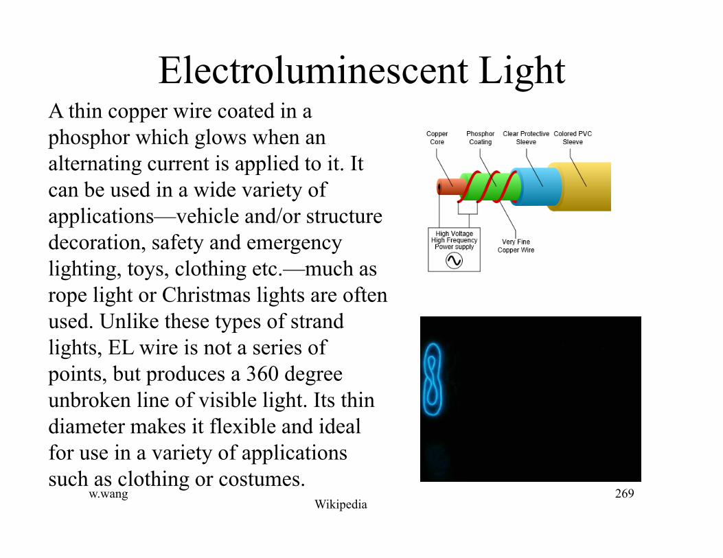
Electroluminescent Light
w.wang 269
A thin copper wire coated in a phosphor which glows when an alternating current is applied to it. It can be used in a wide variety of applications—vehicle and/or structure decoration, safety and emergency lighting, toys, clothing etc.—much as rope light or Christmas lights are often used. Unlike these types of strand lights, EL wire is not a series of points, but produces a 360 degree unbroken line of visible light. Its thin diameter makes it flexible and ideal for use in a variety of applications such as clothing or costumes.
Wikipedia

w.wang 270
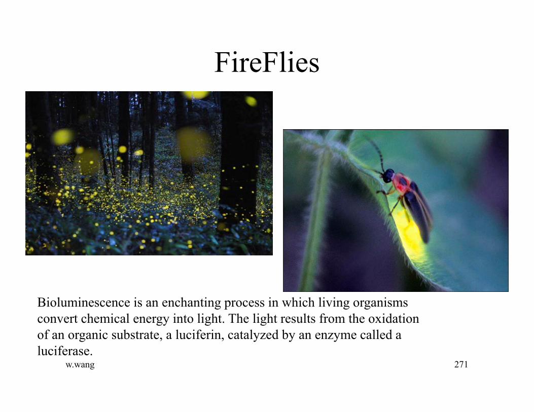
FireFlies
w.wang 271
Bioluminescence is an enchanting process in which living organisms convert chemical energy into light. The light results from the oxidation of an organic substrate, a luciferin, catalyzed by an enzyme called a luciferase.

Luminescence of FireFlies
Fireflies have organs underneath their abdomens that are dedicated to producing light. As they take in oxygen, specialized cells called photocytes produce light as the oxygen combines with luciferin. In a firefly's tail, there are two different chemicals that aid light production: luciferase and luciferin. Luciferase plays a role in heat resistance, and luciferin is an enzyme that triggers light release. Both of these chemicals light up in the presence of ATP (principal molecule for storing and transferring energy in cells), which is the energy source for these reactions. Even as underground larvae or eggs, fireflies produce light. w.wang 272
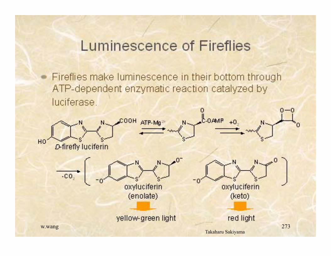
w.wang 273Takaharu Sakiyama