Embed Size (px)
Citation preview
Optical induction scheme for assembling nondiffracting aperiodic Vogel spiralsFalko Diebel, Patrick Rose, Martin Boguslawski, and Cornelia Denz
Citation: Applied Physics Letters 104, 191101 (2014); doi: 10.1063/1.4875237 View online: http://dx.doi.org/10.1063/1.4875237 View Table of Contents: http://scitation.aip.org/content/aip/journal/apl/104/19?ver=pdfcov Published by the AIP Publishing Articles you may be interested in Experimentally observed field–gas interaction in intense optical lattices Appl. Phys. Lett. 103, 244106 (2013); 10.1063/1.4848781 Optical Trapping of Thermoresponsive Microgel Particles by Holographic Optical Tweezers AIP Conf. Proc. 1391, 359 (2011); 10.1063/1.3643549 Optical and Holographic Characteristic of AsSSe Thin Films AIP Conf. Proc. 1203, 650 (2010); 10.1063/1.3322528 Holographic assembly of semiconductor CdSe quantum dots in polymer for volume Bragg grating structures withdiffraction efficiency near 100% Appl. Phys. Lett. 95, 261109 (2009); 10.1063/1.3276914 Large-angular separation of particles induced by cascaded deflection angles in optical sorting Appl. Phys. Lett. 93, 263901 (2008); 10.1063/1.3040697
This article is copyrighted as indicated in the article. Reuse of AIP content is subject to the terms at: http://scitation.aip.org/termsconditions. Downloaded to IP:
128.176.203.134 On: Mon, 12 May 2014 16:03:03
Optical induction scheme for assembling nondiffracting aperiodicVogel spirals
Falko Diebel,a) Patrick Rose, Martin Boguslawski, and Cornelia DenzInstitut f€ur Angewandte Physik and Center for Nonlinear Science (CeNoS), Westf€alische Wilhelms-Universit€atM€unster, 48149 M€unster, Germany
(Received 24 January 2014; accepted 23 February 2014; published online 12 May 2014)
We introduce an experimental approach to realize aperiodic photonic lattices based on
multiplexing of nondiffracting Bessel beams. This holographic optical induction scheme takes
advantage of the well localized Bessel beam as a basis to assemble two-dimensional photonic
lattices. We present the realization of an optically induced two-dimensional golden-angle Vogel
spiral lattice, which belongs to the family of deterministic aperiodic structures. With our technique,
a very broad class of photonic refractive index landscapes now becomes accessible to
optical induction, which could not be realized with established distributed holographic techniques.VC 2014 AIP Publishing LLC. [http://dx.doi.org/10.1063/1.4875237]
The ability to control light propagation by tailoring pho-
tonic band gap (PBG) materials has attracted a lot of atten-
tion within the last decades, and research activities in this
context have led to many groundbreaking developments in
different fields of optics.1 By designing the optical response
properties of materials, such as photonic crystals, photonic
band gaps arise, which can be regarded as the key require-
ment for numerous exciting effects and applications, e.g.,
promising band gap optical waveguides, lasing devices, and
gap solitons in photonic lattices.2–4
Photonic crystals usually show a high amount of sym-
metry, and a large spatial refractive index contrast is required
to result in a complete photonic band gap. Quasiperiodic
photonic lattices with higher rotational symmetries are
known to offer more isotropic band diagrams.5 Moreover,
considering deterministic aperiodic structures, which show
no rotational nor translation symmetries, the realization of
complete PBG materials become more readily achievable.6
This facilitates the construction of artificial materials which
affect and control the propagation properties for a wide range
of optical modes.
One particular aperiodic pattern that shows an isotropic
PBG is the golden angle spiral.7 This structure belongs to the
wider class of Vogel spirals8 whose remarkable properties
have been studied in many different fields of science. In
optics, applications range from enhanced light-matter cou-
pling designs6 and orbital angular momentum encoding9 to
studies about soliton propagation in the nonlinear regime.10
But due to the lack of both, translational and rotational sym-
metries, the fabrication of these structures is very challeng-
ing and mostly relies on point-by-point methods in only one
plane.
For periodic structures, the optical induction method has
proven its powerful ability to create a huge variety of linear
and nonlinear photonic lattices.11,12 By illuminating photo-
sensitive materials with a structured light field, a refractive
index modulation can be induced, following the beam’s in-
tensity distribution. These photonic lattices represent a
highly versatile system to study fundamental linear and non-
linear physics in model experiments, confirmed by many
convincingly demonstrated phenomena.13–16 Over time, the
structural complexity of the realized photonic lattices was
developed from two-dimensional periodic12,15 to quasi-
periodic three-dimensional.17 Moreover, the realization of
multiperiodic superlattices18–20 as well as defect lattices21
further proves the flexibility of the optical induction
approach and thus paves the way towards exciting effects in
complex photonic lattices. However, all these approaches
rely on coherent or incoherent superposition of spatially
extended nondiffracting beams with a high amount of regu-
larity,12,22 which makes it impossible to create two-
dimensional aperiodic structures. Consequently, we have to
further refine this method to be capable of fabricating a
wider class of two-dimensional photonic refractive index
landscapes.
In this contribution, we present an experimental scheme
to optically induce two-dimensional aperiodic photonic latti-
ces based on multiplexing of well localized nondiffracting
Bessel beams.23 In principle, all two-dimensional structures
based on single spots, ranging from small clusters of coupled
waveguides to complex aperiodic arrangements thereby
become accessible to optical induction. This technique
describes a paradigm shift from distributed, parallel methods
towards a point-wise induction approach and provides a very
powerful platform to study the fundamentals of linear and
nonlinear light propagation in aperiodic photonic lattices.
The basic idea behind this approach is to approximate
each site of the desired structure with the transverse profile
of a zero-order nondiffracting Bessel beam, whose transverse
position is given by the addressed two-dimensional structure.
Thereby, it is crucial to avoid coherent superposition, which
will keep the phase relation between the beams and result in
an additional transverse intensity modulation due to interfer-
ence. Consequently, we illuminate the sample with the indi-
vidually positioned Bessel beams one after the other in a fast
sequence, which is repeated multiple times. We utilize that
the buildup of the refractive index modulation is accumula-
tive with time, which is one of the properties of the used pho-
torefractive material. For this method, it is important to
a)Author to whom correspondence should be addressed. Electronic mail:
0003-6951/2014/104(19)/191101/4/$30.00 VC 2014 AIP Publishing LLC104, 191101-1
APPLIED PHYSICS LETTERS 104, 191101 (2014)
This article is copyrighted as indicated in the article. Reuse of AIP content is subject to the terms at: http://scitation.aip.org/termsconditions. Downloaded to IP:
128.176.203.134 On: Mon, 12 May 2014 16:03:03
ensure that the illumination time of each Bessel beam is
small compared to the typical intensity dependent dielectric
relaxation time. For the chosen single beam intensities of
approximately 2.2 mW, the relaxation time is in the range of
tens of seconds.18 The presented incremental multiplexing
approach is expected to have the same effect on the induced
refractive index modulation as a continuous illumination
with an effective two-dimensional intensity pattern, which
would result from incoherent superposition of all nondif-
fracting Bessel beams. The simultaneous incoherent super-
position of a huge number of beams is also possible in
principle, but technically extremely challenging. Therefore,
we here rely on incremental multiplexing methods for the
optical induction.
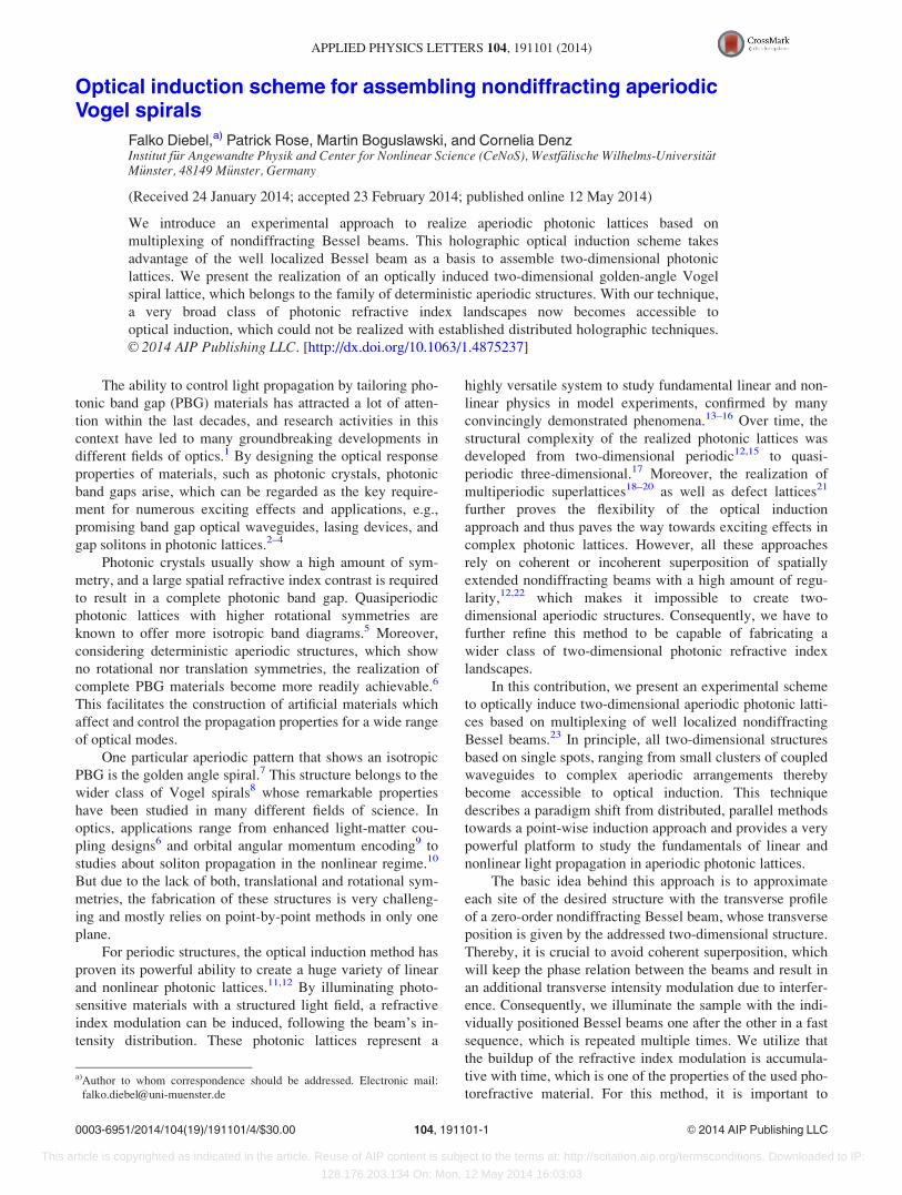
To verify that our approach is capable to assemble dis-
crete two-dimensional index structures, we compare a regu-
lar diamond lattice with its Bessel beam synthesized
counterpart. According to the principle of the proposed
induction scheme, each lattice site is replaced by a same-
sized (FWHM) zero-order Bessel beam, centered at the cor-
responding transverse position. In Fig. 1, the induction beam
intensities, the calculated index modulations and the band
diagram for both cases are shown. Due to the overlapping
side lobes of the adjacent Bessel beams, the intensity pattern
is slightly reshaped and reduced in contrast. However, this
does not remarkably affect the qualitative appearance of the
photonic band diagram, as shown in Figs. 1(c) and 1(f). This
substantiates the proposed point-wise multiplexing scheme
for approximation of many two-dimensional geometries with
Bessel beams.
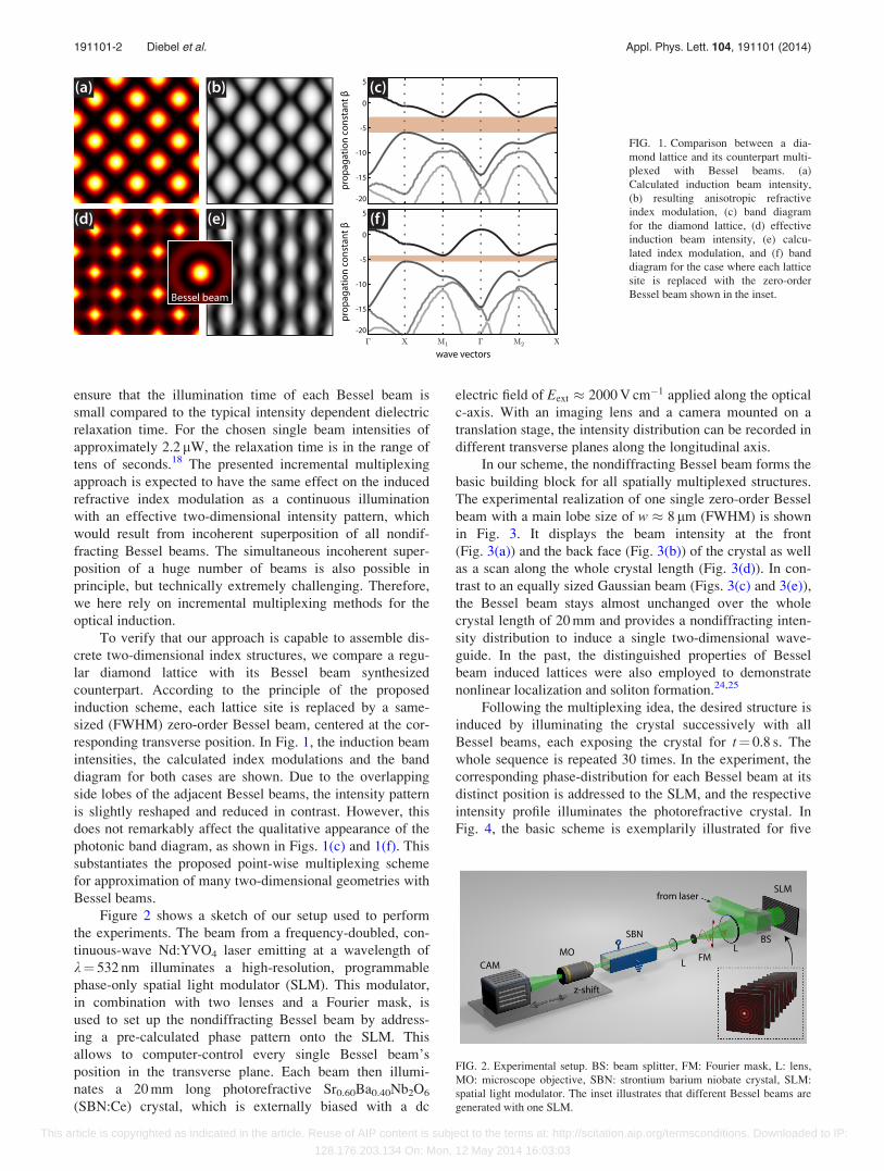
Figure 2 shows a sketch of our setup used to perform
the experiments. The beam from a frequency-doubled, con-
tinuous-wave Nd:YVO4 laser emitting at a wavelength of
k¼ 532 nm illuminates a high-resolution, programmable
phase-only spatial light modulator (SLM). This modulator,
in combination with two lenses and a Fourier mask, is
used to set up the nondiffracting Bessel beam by address-
ing a pre-calculated phase pattern onto the SLM. This
allows to computer-control every single Bessel beam’s
position in the transverse plane. Each beam then illumi-
nates a 20 mm long photorefractive Sr0.60Ba0.40Nb2O6
(SBN:Ce) crystal, which is externally biased with a dc
electric field of Eext � 2000 V cm�1 applied along the optical
c-axis. With an imaging lens and a camera mounted on a
translation stage, the intensity distribution can be recorded in
different transverse planes along the longitudinal axis.
In our scheme, the nondiffracting Bessel beam forms the
basic building block for all spatially multiplexed structures.
The experimental realization of one single zero-order Bessel
beam with a main lobe size of w � 8 mm (FWHM) is shown
in Fig. 3. It displays the beam intensity at the front
(Fig. 3(a)) and the back face (Fig. 3(b)) of the crystal as well
as a scan along the whole crystal length (Fig. 3(d)). In con-
trast to an equally sized Gaussian beam (Figs. 3(c) and 3(e)),
the Bessel beam stays almost unchanged over the whole
crystal length of 20 mm and provides a nondiffracting inten-
sity distribution to induce a single two-dimensional wave-
guide. In the past, the distinguished properties of Bessel
beam induced lattices were also employed to demonstrate
nonlinear localization and soliton formation.24,25
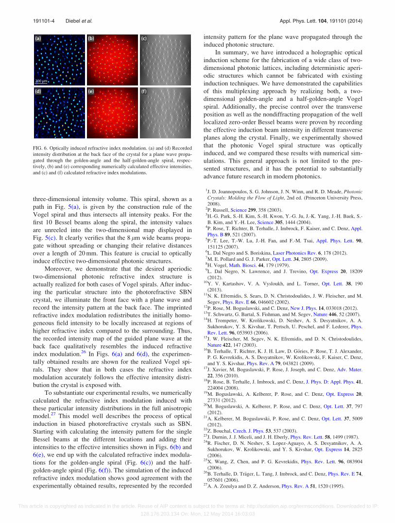
Following the multiplexing idea, the desired structure is
induced by illuminating the crystal successively with all
Bessel beams, each exposing the crystal for t¼ 0.8 s. The
whole sequence is repeated 30 times. In the experiment, the
corresponding phase-distribution for each Bessel beam at its
distinct position is addressed to the SLM, and the respective
intensity profile illuminates the photorefractive crystal. In
Fig. 4, the basic scheme is exemplarily illustrated for five
FIG. 1. Comparison between a dia-
mond lattice and its counterpart multi-
plexed with Bessel beams. (a)
Calculated induction beam intensity,
(b) resulting anisotropic refractive
index modulation, (c) band diagram
for the diamond lattice, (d) effective
induction beam intensity, (e) calcu-
lated index modulation, and (f) band
diagram for the case where each lattice
site is replaced with the zero-order
Bessel beam shown in the inset.
FIG. 2. Experimental setup. BS: beam splitter, FM: Fourier mask, L: lens,
MO: microscope objective, SBN: strontium barium niobate crystal, SLM:
spatial light modulator. The inset illustrates that different Bessel beams are
generated with one SLM.
191101-2 Diebel et al. Appl. Phys. Lett. 104, 191101 (2014)
This article is copyrighted as indicated in the article. Reuse of AIP content is subject to the terms at: http://scitation.aip.org/termsconditions. Downloaded to IP:
128.176.203.134 On: Mon, 12 May 2014 16:03:03
spots forming a two-dimensional cluster of waveguides. The
recorded intensity profile for each single Bessel beam is
shown in Figs. 4(a)–4(e). Their transverse locations were
adjusted to resemble the predetermined structure. The
expected effective intensity profile resulting from the multi-
plexing procedure is shown in Fig. 4(f) as a summation over
individually recorded beam intensities.
The multiplexing scheme described in Fig. 4 can readily be
scaled up to a considerable number of single waveguides to opti-
cally induce even large, complex two-dimensional photonic
structures. One comprehensive example of such a structure is
given by the Vogel spiral. This spiral belongs to the class of
deterministic aperiodic structures and exhibits neither rotational
nor translational symmetries. Therefore, it is not easily realizable
with known holographic optical induction methods. The con-
struction rule for the Vogel spiral is given by the quantization of
the radial and angular variables as r ¼ r0
ffiffiffinp
and u ¼ an, with
n¼ 0…N.6 Here, N is the number of waveguides, r0 is a scaling
factor, and a is an angle which is incommensurable to p. For the
two cases presented in the following, a is set to be the golden
angle and its half, respectively. The golden angle is given by
W¼ 2p/U2, where U ¼ ð1þffiffiffi5pÞ=2 is the golden ratio, which
can also be approximated by Fibonacci numbers fn as
U ¼ limn!1 fn=fn�1.6
In the following, we representatively demonstrate the
optical induction of these two types of Vogel spirals with up
to N¼ 100 single waveguides. Figure 5 shows the experi-
mental results regarding the realization of the effective
induction beam intensity required for the induction of the
golden-angle spiral (Figs. 5(a)–5(c)) and the half-golden-
angle spiral (Figs. 5(d) and 5(e)). Figures 5(a) and 5(b) show
an overlay of the experimentally realized Bessel beam inten-
sities placed at the individual sites of the golden-angle spiral
at the front and the back face of the crystal. To highlight the
accurate spatial placement of all beams, an overlay (Itot) of
all individually recorded intensities (In) is shown according
to Itot ¼ ðP
n IpnÞ
1=p, with p¼ 4. The inset in Fig. 5(b) dis-
plays the resulting effective intensity profile as a digital sum-
mation of all single intensities (p¼ 1).
To verify the nondiffracting nature of this structure in
longitudinal direction, the intensity profile along a spiral
path in the transverse plane is extracted from the recorded
FIG. 3. Nondiffracting Bessel beam. (a) Bessel beam Intensity profile at the
front face of the crystal, (b) intensity at the back face, (c) Gaussian beam in-
tensity in the middle of the crystal, (d) nondiffracting intensity of the Bessel
beam in longitudinal direction, and (e) diffraction of the same-sized
Gaussian beam.
FIG. 4. Scheme of the multiplexing Bessel beam method. (a)–(e) Intensity
profiles of the single experimentally realized Bessel beams, and (f) summa-
tion over the individually recorded intensities. The circles in the pictures
indicate all beam positions.
FIG. 5. Two-dimensional Vogel spirals. (a) Digital overlay (with p¼ 4) of
the individually recorded Bessel beam intensities forming the golden-angle
spiral at the front face of the crystal, (b) corresponding intensity overlay at
the back face, (c) unreeled two-dimensional intensity cross-section through
the three-dimensional volume along the spiral depicted in (a), (d) intensity
overlay for the half-golden-angle spiral at the front face, and (e) at the back
face. The insets in (b) and (e) show the digital superposition of the inten-
sities (with p¼ 1).
191101-3 Diebel et al. Appl. Phys. Lett. 104, 191101 (2014)
This article is copyrighted as indicated in the article. Reuse of AIP content is subject to the terms at: http://scitation.aip.org/termsconditions. Downloaded to IP:
128.176.203.134 On: Mon, 12 May 2014 16:03:03
three-dimensional intensity volume. This spiral, shown as a
path in Fig. 5(a), is given by the construction rule of the
Vogel spiral and thus intersects all intensity peaks. For the
first 10 Bessel beams along the spiral, the intensity values
are unreeled into the two-dimensional map displayed in
Fig. 5(c). It clearly verifies that the 8 lm wide beams propa-
gate without spreading or changing their relative distances
over a length of 20 mm. This feature is crucial to optically
induce effective two-dimensional photonic structures.
Moreover, we demonstrate that the desired aperiodic
two-dimensional photonic refractive index structure is
actually realized for both cases of Vogel spirals. After induc-
ing the particular structure into the photorefractive SBN
crystal, we illuminate the front face with a plane wave and
record the intensity pattern at the back face. The imprinted
refractive index modulation redistributes the initially homo-
geneous field intensity to be locally increased at regions of
higher refractive index compared to the surrounding. Thus,
the recorded intensity map of the guided plane wave at the
back face qualitatively resembles the induced refractive
index modulation.26 In Figs. 6(a) and 6(d), the experimen-
tally obtained results are shown for the realized Vogel spi-
rals. They show that in both cases the refractive index
modulation accurately follows the effective intensity distri-
bution the crystal is exposed with.
To substantiate our experimental results, we numerically
calculated the refractive index modulation induced with
these particular intensity distributions in the full anisotropic
model.27 This model well describes the process of optical
induction in biased photorefractive crystals such as SBN.
Starting with calculating the intensity pattern for the single
Bessel beams at the different locations and adding their
intensities to the effective intensities shown in Figs. 6(b) and
6(e), we end up with the calculated refractive index modula-
tions for the golden-angle spiral (Fig. 6(c)) and the half-
golden-angle spiral (Fig. 6(f)). The simulation of the induced
refractive index modulation shows good agreement with the
experimentally obtained results, represented by the recorded
intensity pattern for the plane wave propagated through the
induced photonic structure.
In summary, we have introduced a holographic optical
induction scheme for the fabrication of a wide class of two-
dimensional photonic lattices, including deterministic aperi-
odic structures which cannot be fabricated with existing
induction techniques. We have demonstrated the capabilities
of this multiplexing approach by realizing both, a two-
dimensional golden-angle and a half-golden-angle Vogel
spiral. Additionally, the precise control over the transverse
position as well as the nondiffracting propagation of the well
localized zero-order Bessel beams were proven by recording
the effective induction beam intensity in different transverse
planes along the crystal. Finally, we experimentally showed
that the photonic Vogel spiral structure was optically
induced, and we compared these results with numerical sim-
ulations. This general approach is not limited to the pre-
sented structures, and it has the potential to substantially
advance future research in modern photonics.
1J. D. Joannopoulos, S. G. Johnson, J. N. Winn, and R. D. Meade, PhotonicCrystals: Molding the Flow of Light, 2nd ed. (Princeton University Press,
2008).2P. Russell, Science 299, 358 (2003).3H.-G. Park, S.-H. Kim, S.-H. Kwon, Y.-G. Ju, J.-K. Yang, J.-H. Baek, S.-
B. Kim, and Y.-H. Lee, Science 305, 1444 (2004).4P. Rose, T. Richter, B. Terhalle, J. Imbrock, F. Kaiser, and C. Denz, Appl.
Phys. B 89, 521 (2007).5P.-T. Lee, T.-W. Lu, J.-H. Fan, and F.-M. Tsai, Appl. Phys. Lett. 90,
151125 (2007).6L. Dal Negro and S. Boriskina, Laser Photonics Rev. 6, 178 (2012).7M. E. Pollard and G. J. Parker, Opt. Lett. 34, 2805 (2009).8H. Vogel, Math. Biosci. 44, 179 (1979).9L. Dal Negro, N. Lawrence, and J. Trevino, Opt. Express 20, 18209
(2012).10Y. V. Kartashov, V. A. Vysloukh, and L. Torner, Opt. Lett. 38, 190
(2013).11N. K. Efremidis, S. Sears, D. N. Christodoulides, J. W. Fleischer, and M.
Segev, Phys. Rev. E 66, 046602 (2002).12P. Rose, M. Boguslawski, and C. Denz, New J. Phys. 14, 033018 (2012).13T. Schwartz, G. Bartal, S. Fishman, and M. Segev, Nature 446, 52 (2007).14H. Trompeter, W. Krolikowski, D. Neshev, A. S. Desyatnikov, A. A.
Sukhorukov, Y. S. Kivshar, T. Pertsch, U. Peschel, and F. Lederer, Phys.
Rev. Lett. 96, 053903 (2006).15J. W. Fleischer, M. Segev, N. K. Efremidis, and D. N. Christodoulides,
Nature 422, 147 (2003).16B. Terhalle, T. Richter, K. J. H. Law, D. G€ories, P. Rose, T. J. Alexander,
P. G. Kevrekidis, A. S. Desyatnikov, W. Krolikowski, F. Kaiser, C. Denz,
and Y. S. Kivshar, Phys. Rev. A 79, 043821 (2009).17J. Xavier, M. Boguslawski, P. Rose, J. Joseph, and C. Denz, Adv. Mater.
22, 356 (2010).18P. Rose, B. Terhalle, J. Imbrock, and C. Denz, J. Phys. D: Appl. Phys. 41,
224004 (2008).19M. Boguslawski, A. Kelberer, P. Rose, and C. Denz, Opt. Express 20,
27331 (2012).20M. Boguslawski, A. Kelberer, P. Rose, and C. Denz, Opt. Lett. 37, 797
(2012).21A. Kelberer, M. Boguslawski, P. Rose, and C. Denz, Opt. Lett. 37, 5009
(2012).22Z. Bouchal, Czech. J. Phys. 53, 537 (2003).23J. Durnin, J. J. Miceli, and J. H. Eberly, Phys. Rev. Lett. 58, 1499 (1987).24R. Fischer, D. N. Neshev, S. Lopez-Aguayo, A. S. Desyatnikov, A. A.
Sukhorukov, W. Krolikowski, and Y. S. Kivshar, Opt. Express 14, 2825
(2006).25X. Wang, Z. Chen, and P. G. Kevrekidis, Phys. Rev. Lett. 96, 083904
(2006).26B. Terhalle, D. Tr€ager, L. Tang, J. Imbrock, and C. Denz, Phys. Rev. E 74,
057601 (2006).27A. A. Zozulya and D. Z. Anderson, Phys. Rev. A 51, 1520 (1995).
FIG. 6. Optically induced refractive index modulation. (a) and (d) Recorded
intensity distribution at the back face of the crystal for a plane wave propa-
gated through the golden-angle and the half-golden-angle spiral, respec-
tively, (b) and (e) corresponding numerically calculated effective intensities,
and (c) and (f) calculated refractive index modulations.
191101-4 Diebel et al. Appl. Phys. Lett. 104, 191101 (2014)
This article is copyrighted as indicated in the article. Reuse of AIP content is subject to the terms at: http://scitation.aip.org/termsconditions. Downloaded to IP:
128.176.203.134 On: Mon, 12 May 2014 16:03:03