Embed Size (px)
Citation preview

Air Force Institute of TechnologyAFIT Scholar
Theses and Dissertations Student Graduate Works
3-11-2011
Optical and Electrical Characterization Melt-grownBulk InGaAs and InAsPJean W. Wei
Follow this and additional works at: https://scholar.afit.edu/etd
Part of the Optics Commons
This Dissertation is brought to you for free and open access by the Student Graduate Works at AFIT Scholar. It has been accepted for inclusion inTheses and Dissertations by an authorized administrator of AFIT Scholar. For more information, please contact [email protected].
Recommended CitationWei, Jean W., "Optical and Electrical Characterization Melt-grown Bulk InGaAs and InAsP" (2011). Theses and Dissertations. 1479.https://scholar.afit.edu/etd/1479
OPTICAL AND ELECTRICAL CHARACTERIZATION OF MELT-GROWN
BULK INDIUM GALLIUM ARSENIDE AND INDIUM ARSENIC PHOSPHIDE
ALLOYS
DISSERTATION
JEAN WEI
AFIT/DS/ENP/11-M02
DEPARTMENT OF THE AIR FORCE
AIR UNIVERSITY
AIR FORCE INSTITUTE OF TECHNOLOGY
Wright-Patterson Air Force Base, Ohio
APPROVED FOR PUBLIC RELEASE; DISTRIBUTION UNLIMITED

The views expressed in this dissertation are those of the author and do not reflect
the official policy or position of the United States Air Force, the Department of Defense,
or the United States Government. This material is declared a work of the U.S.
Government and is not subject to copyright protection in the United States.

AFIT/DS/ENP/11-M02
OPTICAL AND ELECTRICAL CHARACTERIZATION OF MELT-
GROWN BULK INDIUM GALLIUM ARSENIDE AND INDIUM
ARSENIC PHOSPHIDE ALLOYS
DISSERTATION
Presented to the Faculty
Department of Engineering Physics
Graduate School of Engineering and Management
Air Force Institute of Technology
Air University
Air Education and Training Command
In Partial Fulfillment of the Requirements for the
Degree of Doctor of Philosophy
Jean Wei, BS, MS
March 2011
APPROVED FOR PUBLIC RELEASE; DISTRIBUTION UNLIMITED

AFIT/DS/ENP/11-M02
OPTICAL AND ELECTRICAL CHARACTERIZATION OF MELT-GROWN
BULK INDIUM GALLIUM ARSENIDE AND INDIUM ARSENIC PHOSPHIDE
ALLOYS
Jean Wei, BS, MS
Approved:
____________________________________
Yung Kee Yeo, PhD (Chairman)
____________________________________
Robert Hengehold, PhD (Member)
____________________________________
Shekhar Guha, PhD (Member)
____________________________________
Mark Oxley, PhD (Member)
Accepted:
____________________________________
M. U. Thomas
Dean, Graduate School of
Engineering and Management
__________________
Date
__________________
Date
__________________
Date
__________________
Date
__________________
Date

iv
AFIT/DS/ENP/11-M02
Abstract
Optical and electrical properties of bulk melt-grown ternary InAs1-yPy and
InxGa1-xAs polycrystals were investigated as functions of phosphorus and indium
compositions and temperatures using the photoluminescence, Fourier transform
infrared (FTIR) transmission spectrum, refractive index, and Hall-effect measurements.
These ternary alloys were grown using the vertical Bridgman techniques. The as-grown
undoped bulk ternary InAs1-yPy and InxGa1-xAs polycrystals have been found to exhibit
n-type conductivity irrespective of the alloy compositions possibly due to residual
impurities and native defects. In general, carrier concentrations and Hall mobilities
increase with the indium composition for InxGa1-xAs, whereas they decrease with
increasing phosphorus mole fraction for the InAs1-yPy sample. The FTIR spectra of all
these ternary samples demonstrated good infrared transmission. A systematic
measurement of photoluminescence was carried out in order to gain insight into the
various radiative transitions in the InAs1-yPy and InxGa1-xAs crystals, which include the
temperature, laser excitation power, and sample location dependent studies. The
wavelength, temperature, and composition dependent refractive indices of InAs1-yPy and
InxGa1-xAs were studied using minimum deviation and Michelson Fabry-Perot
interferometry methods. The measured results of refractive indices, transport properties,
bandgap energies, and optical transmissions are presented here as functions of alloy
composition, temperature and photon energy for the first time, to the best of our
knowledge. Although the bulk InAs1-yPy and InxGa1-xAs samples show good optical

v
transmissions, PL transitions, and high carrier mobilities, they do exhibit some random
compositional fluctuations across the sample. A practical method of extracting
bandgap energies directly from the FTIR transmission spectra has been presented in this
work, and the results are promising even though further refinement is required.
Bandgap energies estimated from the transmission spectra agree well with those
obtained from PL spectra and the previously reported values from the thin film studies.
Overall, the optical and electrical properties of these crystals are well suited for a
variety of device applications that do not require single crystalline material.

vi
Acknowledgments
Writing this dissertation has been one of the greatest challenges of my life. Without
the support and guidance of my colleagues, family and friends, I would never have been able
to complete it. First of all, I must thank Dr. Yung Kee Yeo, my advisor, who deserves
many thanks for all of his advice, corrections, and insight throughout the project. His
assistance was indispensible. Dr. Shekhar Guha, Dr. Leo Gonzalez, Dr. Joel Murray, and
Jacob Barnes, Derek Upchurch, and Amelia Carpenter from IR Lab were also invaluable.
They offered countless tips on the experimental design and minutiae of lab equipment,
provided help in trouble shooting, and set things straight when I came perilously close to
serious damage. Without them I would probably be wandering in the darkness. Thanks
to Dr. Glen Gillen from California Polytechnic, who developed the interferometry
refractive index measurement and trained me in its use. Thanks to Dr. Elizabeth Moore
who trained me to use the Hall system at AFIT. Dr. Mee-Yi Ryu was also of great
assistance as her kindness, needed guidance, and useful discussions were critical to my
success. Thanks to 1st Lt Austin Bergstrom who had made the PL system finally works.
Thanks to Partha Dutta and Geeta Rajagopalan; they provided me 99% of the samples in
this work. Thanks to Steve Molla, who has offered consistent support and reviewed my
drafts for typos and grammar errors. Last but not least, thanks to my family (my daughter
and my parents), for without them this effort would be worth nothing. Their love, patience,
and support gave me the foundation I needed to complete this study.
Jean Wei

vii
Table of Contents
Page
Abstract .............................................................................................................................. iv
Acknowledgments.............................................................................................................. vi
List of Figures .................................................................................................................... ix
List of Tables .....................................................................................................................xv
1. Introduction ..................................................................................................................1
Motivation ....................................................................................................................1
Objective.......................................................................................................................4
Approach ......................................................................................................................5
Dissertation Summary and Layout ...............................................................................5
2. Theory ..........................................................................................................................7
Semiconductor Basics ..................................................................................................7
Bulk III-V Ternary Crystal Growth ..............................................................................8
Band Structure and Bandgap Energy .........................................................................11
Temperature Effects on Semiconductors ....................................................................15
Semiconductor Impurities ..........................................................................................17
3. Characterization Techniques and Experimental Setups .............................................19
Electrical Characterization .........................................................................................19
Hall-effect Theory ................................................................................................... 19
Hall-effect Measurement System ............................................................................. 23
Optical Characterization .............................................................................................25
Fourier Transform Infrared Spectroscopy ............................................................... 25
Photoluminescence Measurement ............................................................................ 27
Refractive Index .........................................................................................................34
Prism Based Measurement Using Minimum Deviation Method .............................. 34
Wafer Based Measurement Using Michelson and Fabry-Perot Interferometer ...... 35
Electron Probe Micro Analyzer (EPMA) ...................................................................40
Infrared Imagery .........................................................................................................42
4. Results and Discussions of Binary InAs, InP, and GaAs ...........................................45
Purpose .......................................................................................................................45
Determination of Bandgap Energy .............................................................................45

viii
Page
Bandgap Energy Obtained from Transmission Spectra for InAs ............................ 48
Temperature Dependent Bandgap Energy Obtained from Transmission Spectra ......52
Temperature Dependent Bandgap of InAs ............................................................... 53
Temperature Dependent Bandgap of InP................................................................. 60
Temperature Dependent Bandgap of GaAs ............................................................. 65
Determination of dn/dT from dEg/dT .........................................................................68
Refractive-Index Measurements .................................................................................69
5. Results and Discussions on Bulk Ternary InAs1-yPy ..................................................73
Ternary InAs1-y Py Crystal Growth .............................................................................73
Bulk InAs1-x Py Crystal Images ..................................................................................76
Bandgap Energy of Bulk InAs1-yPy ............................................................................78
Photoluminescence Measurements .............................................................................81
Refractive Index Measurements .................................................................................91
Hall-effect Measurements ..........................................................................................96
6. Results and Discussions on Bulk Ternary InxGa1-xAs ................................................99
Ternary InxGa1-xAs Crystal Growth ...........................................................................99
Bandgap Energy of Bulk InxGa1-xAs ........................................................................101
Photoluminescence Studies ......................................................................................104
Sample Location Dependent PL Measurements.................................................... 105
Laser Excitation Power Dependent PL Measurements......................................... 108
Temperature Dependent PL Measurements ........................................................... 113
Refractive Index Measurements ...............................................................................119
Hall-effect Measurements ........................................................................................120
7. Conclusions and Future Work ..................................................................................122
Appendix A ......................................................................................................................128
Appendix B ......................................................................................................................129
Appendix C ......................................................................................................................134
Bibliography ....................................................................................................................137

ix
List of Figures
1.1. Bandgap energy vs. lattice constant (Å) at 300 K for various
III-V semiconductors. ................................................................................................ 2
2.1. Crystal lattice structure .............................................................................................. 8
2.2. A schematic pseudobinary phase diagram of a
III-V ternary compound(GaInSb) .............................................................................. 9
2.3. Schematic lattice constant match and mismatch effects
on the quality of crystal............................................................................................ 10
2.4. Vertical Bridgman growth of Ga1-xInxSb system ..................................................... 11
2.5. A typical bandgap structure ..................................................................................... 12
2.6. Illustration of band structures of semiconductor materials ...................................... 15
3.1. A schematic diagram illustrating of the van der Pauw Hall-effect .......................... 21
3.2. A schematic diagram of the LakeShore 7505 automated
Hall measurement system ........................................................................................ 24
3.3. A schematic layout of Perkin Elmer Spectrum GX FTIR
system with the PC interface.................................................................................... 27
3.4. Common radiative transitions take place in semiconductors.
(a) band-to-band, (b) free exciton, (c) neutral donor
and free hole recombination, (d) a free electron transitioning
to a neutral shallow acceptor, and (e) (f) donor-acceptor transitions
for shallow and deep states, respectively. ................................................................ 29
3.5. Experimental setup for the PL measurement ........................................................... 32
3.6. (a) Illustration of a ray of light dispersed through a prism, and
(b) deviation angle vs. incident angle. Red data points are
measured at 295 K and blue at 100 K with an InP prism at 4.6 m. ....................... 34
3.7. (a) Prism dimensions (b) Minimum deviation method experimental layout ........... 35
3.8. Schematic Michelson and Fabry-Perot interferometers layout ................................ 36
Figure Page

x
3.9. Illustration of optical path nd changing with rotating angle ................................. 37
3.10. (Top) Michelson interferometer interference pattern observed
at a detector; (Bottom) phase information extracted from the
interference pattern for both setups and their difference ........................................ 38
3.11. (Top) Electron probe micro analyzer (EPMA): CAMECA 100.
(Bottom) a typical analysis spectrum of EPMA ..................................................... 41
3.12. Santa Barbara focaplance image IR infrared camera ............................................. 42
3.13. MIR imaging system using Santa Barbara Focalplane ImagIR ............................. 43
3.14. MIR images of six InAs crystals using Santa Barbara focal plane
infrared camera ...................................................................................................... 44
4.1. (a) A theoretical graph of the absorption coefficient and its
first derivative in a uniform bulk sample showing a sharp peak
of the derivative in the vicinity of the bandgap. (b) The second derivative
of the absorption coefficient for different values of bandgap variation
within the sample. .................................................................................................... 48
4.2. (a) Transmission spectra of InAs 143 samples with five thicknesses
(b) d(-T)/dE vs. E. Peak locations are defined as EL min.
(c) d2(-T)/dE
2 vs. E. The minimum locations are defined as EL max.
E is a photon energy. ................................................................................................ 50
4.3. EL min and EL max vs. sample thickness for a set of InAs 143 samples....................... 51
4.4. (top) Temperature dependent transmission spectra of InAs
sample WT 524-10; (bottom) temperature dependent dE
dT
plotted as a function of photon energy ..................................................................... 54
4.5. EL min (red dot) extracted from transmission spectra of InAs
and bandgap energy of InAs by Fang et al. (solid curve) ........................................ 55
4.6. Etln(dC) vs. temperature and a fitting curve with Eg – EL min = Tb,
with b=0.5 ................................................................................................................ 56
4.7. Temperature dependent bandgap energy obtained from transmission
spectra (red dots) and published results (solid curve) by Fang, et al. ...................... 57
Figure Page

xi
4.8. Temperature dependent transmission spectra of three InAs
samples (a) InAs WT 524-11 (b) InAs D1 (c) InAs 100 ......................................... 58
4.9. Temperature dependent bandgap energies of four InAs samples (symbols).
The solid curve is temperature dependent bandgap energies
reported by Fang et al. ............................................................................................. 59
4.10. Temperature dependent transmission spectra of three
InP samples (a) InP B2 (b) InP R3781 un (c) InP 6................................................. 61
4.11. dE
d T)1( vs. E for InP sample at various temperatures
(a) InP sample B2. (b) InP sample R3781_un ....................................................... 62
4.12. (top) EL min (symbols) of three InP samples and published
Eg (solid curve). (bottom) (Eg -EL min) plotted as a function of temperature.
The curve is fitted with a power series function of Tb with b=0.5 ....................... 63
4.13. Temperature dependent bandgap energies obtained from transmission
spectra (triangle, dot, and square) for three InP samples and published
bandgap energies (solid curve). .............................................................................. 64
4.14. (a), (b) and (c) Temperature dependent transmission spectra of three
GaAs samples of GaAs 82, GaAs WV 19557 and GaAs 12472-24,
respectively. (d) d(1-T)/dE of GaAs 12472-24 plotted as a function
of photon energy. ................................................................................................... 66
4.15. (a) Extracted EL min of three GaAs samples (symbols) and published
Eg values (solid curve). (b) Temperature dependent bandgap energies
of three GaAs samples obtained from transmission spectra
(#, dot, and square) and published Eg values (solid curve) .................................... 67
4.16. Obtained values of the material plotted as a function of material’s
refractive index ...................................................................................................... 68
4.17. Prism angle measurement setup ............................................................................. 70
4.18. (a) Temperature dependent refractive indices of InAs measured at
three wavelengths, 3.39, 4.6 and 10.6 m
(b) Best fit curve for dn/dT vs. wavelength ........................................................... 70
Figure Page

xii
4.19. (a) Temperature dependent refractive index of InP measured at four
wavelengths of 1.55, 3.39, 4.6 and 10.6 m. (b) Best fit curve
for dn/dT vs. wavelength. ...................................................................................... 71
5.1. Crystal boul and crystal wafer of an InAs1-yPy crystal ............................................. 75
5.2. Prism used in refractive index measurements using minimum deviation method... 76
5.3. MIR images of InAs1-yPy crystal samples ................................................................ 76
5.4. Images of a laser beam at 4.6 m, before or passing through InAs1-yPy crystals ..... 78
5.5. (Top) Transmission spectra of six InAs1-yPy samples with composition
ranging from 0.19 to 0.66; (Bottom) the 1st derivatives of transmission
spectra with respect to photon energy plotted as a function
of photon energy ...................................................................................................... 80
5.6. EL min values obtained from transmission spectra (red dots)
plotted as a function of phosphorus composition. The solid line
is the bandgap energies of InAs1-yPy calculated from equation 5.1 ......................... 81
5.7. Location dependent PL spectra of a InAs0.81P0.19 sample taken at 12 K
with a laser excitation power of 300 mW ................................................................ 82
5.8. Photoluminescence spectra of InAs0.81P0.19 sample measured at 12 K
at different incident laser powers. ............................................................................ 84
5.9. Integrated photoluminescence intensities of peaks A and B for
InAs0.81P0.19 sample measured at 12 K plotted as a function
of excitation power. ................................................................................................. 85
5.10. Temperature dependent PL spectra of the InAs0.81P0.19 with a laser power
of 300 mW ............................................................................................................... 86
5.11. FX peak of InAs0.81P0.19 (red) and ELmin (black) vs. Temperature.
Eg (blue) is calculated using Eq. TEE Lg min . ....................................................... 88
5.12. FX peak (red dots) and EL min (black) of InAs0.81P0.19vs. Temperature.
Eg is calculated using Eq. TEE Lg min (blue), and the Varshni
equation solid black line .......................................................................................... 89
Figure Page

xiii
5.13. Temperature dependent bandgap energy of InAs1-yPy and their
linear fit ................................................................................................................. 90
5.14. Refractive index of InAs0.81P0.19 alloy as a function of temperature ..................... 92
5.15. Refractive index of InAs0.81P0.19 alloy as a function of wavelength ...................... 93
5.16. Refractive Index of InAs0.81P0.19 measured at 4.6 m, and
at 95 K and 295 K as a function of composition.................................................... 94
5.17. Measured dn/dT values of InAs1-yPy alloy for y=0.00, 0.19, 1.00 ......................... 95
5.18. Hall-effect measurement data at 77 and 295 K for various InAs1-yPy
samples as a function of phosphorus mole fraction:
(a) carrier concentration and (b) Hall mobility. ..................................................... 96
5.19. Temperature dependent Hall-effect measurements for the InAs0.9P0.1
from 20 to 310K ...................................................................................................... 97
6.1. Crystal boul (a), crystal wafer (b), and Mid IR image (c) of InxGa1-xAs ............... 101
6.2. (Top) Room temperature transmission spectra of various InxGa1-xAs samples.
(Bottom) First derivatives of transmission spectra with respect to
photon energy plotted as a function of photon energy. For x = 0,
the peak position should be read from the top horizontal scale, and for
the rest of x ≥ 0.75, the peak positions should be read from the
bottom horizontal scale. ......................................................................................... 103
6.3. The estimated bandgap energy Eg = (EL min +0.03x+0.045(1-x)) from
transmission spectra (red dot) for InxGa1-xAs plotted as a function of
In mole fraction. The solid curve represents banggap energies obtained
from the published thin film Eg equation. .............................................................. 104
6.4. Location dependent photoluminescence spectra of In0.75Ga0.25As measured
at 12 K with a laser incident excitation power of 100 mW ................................... 105
6.5. Position-dependent photoluminescence spectra for the In0.82Ga0.18As
measured at 12 K at five different positions with a laser excitation
power of 100 mW .................................................................................................. 107
6.6. Excitation power dependent PL spectra for In0.75Ga0.25As measured at 12 K. ...... 109
Figure Page
xiv
6.7. Integrated photoluminescence intensities of peak A for the
In0.75Ga0.25As sample measured as a function of laser power at 12 K. .................. 110
6.8. Excitation power dependent PL spectra for In0.82Ga0.18 As measured at 12 K. ..... 111
6.9. Integrated photoluminescence intensities of peaks A and B for the
In0.82Ga0.19As sample measured as a function of laser power at 12 K. .................. 112
6.10. Temperature dependent PL spectra for In0.75Ga0.25As with a laser power
of 300 mW ............................................................................................................. 114
6.11. Temperature dependent PL spectra for the In0.82Ga0.18As sample ........................ 115
6.12. Temperature dependent transmission spectra (a) In0.75Ga0.25As;
(b)In0.82Ga0.18As .................................................................................................... 116
6.13. Temperature dependent B-B transition nergies of In0.75Ga0.25As sample
taken at two sample locations. (Red dot taken at spot B and blue square
taken at spot C) along with EL min (black triangle) obtained from
transmission spectra .............................................................................................. 117
6.14. (a) Temperature dependent FX peaks (red dots) and EL min (blue square)
of the In0.82Ga0.18As. (b) Eg (black triangle) calculated using
TEE Lg min with = 0.0035 eVK
-0.5 plotted as a function of
temperature. The solid curve is Varshni equation fit ........................................... 117
6.15. Refractive indices of bulk InxGa1-xAs measured at 100 K and
295 K using Michelson and Fabry-perot method (a) measured at 4.6 m;
(b) measured at 10.6 m.. ..................................................................................... 119
6.16. Hall-effect measurement results at 77 and 300 K for various InxGa1-xAs
samples as a function of indium mole fraction: (a) carrier concentration
and (b) Hall mobility.. ........................................................................................... 121
Figure Page

xv
List of Tables
3.1 List of samples used in the PL experiments and their composition .......................... 33
3.2 Refractive index calibration results of a ISP Optics Si window and
published results of Si ............................................................................................... 40
4.1 InAs Samples investigated ........................................................................................ 57
4.2 InP Sample Information ............................................................................................ 60
4.3 GaAs sample information ......................................................................................... 65
4.4 Comparison between calculated dn/dT and experimental dn/dT .............................. 69
4.5 Comparison between calculated dn/dT and experimental dn/dT .............................. 72
5.1 Bulk ternary InAs1-yPy sample information .............................................................. 76
5.2 Composition dependent Varshni coefficients summary for InAs1-yPy ...................... 90
5.3 Temperature dependent Cauchy coefficients for InAs1-yPy alloy ............................. 92
5.4 Comparison of theoretical and experimental dn/dT for InAs0.81P0.19
alloy........................................................................................................................... 95
6.1 InxGa1-xAs crystal information ................................................................................ 102
6.2 Composition-dependent Varshni coefficients for InxGa1-xAs ................................. 118
6.3 Refractive index of InxGa1-xAs as a function of composition
at various wavelengths and temperatures ............................................................... 120
Table Page

1
OPTICAL AND ELECTRICAL CHARACTERIZATION OF
MELT-GROWN BULK InxGa1-xAs AND InAs1-yPy ALLOYS
1. Introduction
Ternary crystals such as InxGa1-xAs and InAs1-yPy are direct bandgap
semiconductors with bandgaps ranging from 0.36 eV to 1.42 eV for InxGa1-xAs and from
0.36 eV to 1.35 eV for InAs1-yPy shown in Fig. 1.1 [1]. Their applications include near to
mid infrared light sources such as light emitting diodes (LEDs) and lasers diodes (LDs)
[2-9], infrared photo detectors [10-12], high electron mobility transistor (HEMT) devices
[13-14], and low bandgap (0.5-0.7 eV) thermophotovoltaic energy conversion devices
[15-16]. Early characterization studies for these materials trace back to as early as 1978
[17], but most of these previous studies concentrated on epitaxial films [18-21] grown on
bulk binary substrate materials. Bulk sample of InxGa1-xAs and InAs1-yPy were not
commercially available until recently.
1.1 Motivation
These direct bandgap semiconductors are good candidates for Short Wavelength
Infrared (SWIR) and Middle Wave Infrared (MWIR) optoelectronic devices due to their
bandgap range.
In the past, InxGa1-xAs and InAs1-yPy ternary thin films were grown on lattice
matched or mismatched binary semiconductors such as GaAs, InP, and InAs. Since the
lattice constants of GaAs, InP and InAs are 5.6532, 5.8687, and 6.0584 Å, respectively,

2
as shown in Fig. 1.1 [1], the ability to grow thick, high-quality epitaxial layers of
InxGa1-xAs and InAs1-yPy on a GaAs, InP, or InAs substrate is very limited due to lattice
mismatch except for a specific composition [22-25]. For example, only In0.53Ga0.47As
lattice matches to InP, and thus very good quality thick films of this composition can be
grown on InP. The strained critical thickness of an InxGa1-xAs or InAs1-yPy epitaxial layer
depends on the extent of the lattice mismatch between the ternary epitaxial layer and the
binary substrates, normally < 1 m. Also, the strained epitaxial layers grown on lattice
mismatched substrates may have strain-induced crystalline defects, which are known cause
for dislocations, rough surface morphologies, and interface cracking [26-30]. In order to
overcome the limits imposed by lattice mismatch, researchers have tried to pursue
growing bulk ternary semiconductor substrates [31-35].
Figure 1.1. Bandgap energy vs. lattice constant (Å) at 300 K for various III-V semiconductors.
The bulk III-V ternary InxGa1-xAs and InAs1-yPy alloys provide many advantages
over epitaxial layers that are grown on binary III-V compound crystals. First, the bulk
3
ternary alloys can be used as new substrates to grow lattice matched, high quality epitaxial
layers with a large thickness for a wide range of compositions and bandgaps. This provides
for extra freedom and more opportunities for advancing novel optoelectronic device
designs and bandgap engineering. Second, bulk growth is cost effective, and there is
strong potential for developing bulk InxGa1-xAs and InAs1-yPy devices, thus avoiding the
expensive and time-consuming epitaxial deposition.
In spite of the promising advantages of bulk InxGa1-xAs and InAs1-yPy alloys, the
utilization of these materials for efficient optoelectronic devices has been hampered by
the challenges associated with their growth challenges. Bulk ternary crystal growth
requires stringent control over the synthesis conditions in order to avoid crystal defects.
The most serious problem encountered in melt-grown bulk ternary material is cracking.
Cracking is likely due to the combined results of a large lattice/composition mismatch
between the seed and the first-to-freeze crystal, constantly changing composition along
the length, and the induced stress due to growth in a steep thermal gradient. Other crystal
growth problems such as precipitates, inclusions, residual impurities, high native defect
concentrations, and compositional variation across the substrate and from wafer to wafer
are also present. In the future, the quality of bulk ternary alloys must improve greatly
from its current state.
Since prior research on InxGa1-xAs and InAs1-yPy alloy systems was limited to a
narrow composition range [12, 36-38], adequate knowledge of the optical and electrical
properties of this ternary system is lacking. Systematic studies of carrier concentration,
mobility, and resistivity for the InxGa1-xAs and InAs1-yPy alloy systems as functions of
composition have not yet been reported although some work have been reported on

4
InGaAs films [39-40]. Information on the electrical properties of these materials is not
only important to electronic device applications, but can also be correlated to optical
properties such as carrier concentration dependent optical absorption [41].
For optical device applications, for example, those in waveguide configuration,
the refractive index of the active material and substrate must be known to a high accuracy
(on the order of 10-4
), while current reported values have accuracy on the order of 10-1
[42,43]. Furthermore, for nonlinear optical applications, such as smart optical switches,
it is important to know the temperature dependent refractive index values. Unfortunately,
they are not available in the current literature. Previous refractive index results of ternary
semiconductors were limited to theoretical calculations deduced from known binary
property parameters [42, 43]. Refractive index measurements on quaternary InGaAsP
epitaxial layers grown on InP have been reported [17, 44], but temperature dependent
refractive index values of InxGa1-xAs and InAs1-yPy have not yet been reported. Also, it is
necessary to compare properties measured from thin film and from bulk material in order
to provide accurate information of the material.
1.2 Objective
The objective of this study is to investigate the electrical and optical properties of
melt-grown bulk ternary InxGa1-xAs and InAs1-yPy alloys as functions of composition and
temperature using various characterization methods such as Fourier Transform Infrared
(FTIR) transmission spectrum, Hall-effect, photoluminescence (PL), and refractive index
measurement techniques to determine relevant material parameters such as transmission
cut-off wavelength, carrier concentration, mobility, bandgap energy, refractive index, and

5
composition homogeneity. It is aimed at a systematic investigation across a full
composition range of indium and phosphorus mole fractions and at a temperature range
from cryogenic temperature to above room temperature. This study aims to a better
understanding of these relatively new bulk III-V ternary crystal properties.
1.3 Approach
Traditional characterization techniques such as Fourier transmission infrared
spectroscopy, photoluminescence, and Hall-effect measurement methods were employed
in this study. In addition, Electron Probe Micro Analyzer (EPMA) as well as infrared
imagery was also used.
Specific goals of this investigation are:
a. Determination of bandgap energies of bulk InxGa1-xAs and InyAs1-yPy as functions
of composition and temperature using FTIR transmission spectra and PL spectra.
b. Measurements of carrier concentration, mobility, and resistivity of melt-grown
bulk InxGa1-xAs and InyAs1-yPy alloys as functions of composition and temperature
using Hall-effect measurements.
c. Refractive index measurements of the alloys as functions of composition, photon
energy, and temperature using minimum deviation method and Michelson Fabry-
Perot interferometers. Exploiting compositional homogeneity within the wafers
using both EPMA and photoluminescence methods.
1.4 Dissertation Summary and Layout
In this dissertation, literature surveys are presented at the beginning as a part of
the introduction. Relevant background theories are described in chapter 2. This is
followed, by descriptions of measurement techniques used in this work, as well as details
of the experiments and experimental layouts in chapter 3. Chapter 4 describes the first
set of experimental results obtained from binary semiconductors. Chapters 5 and 6

6
contain experimental results and discussions. The discussions also include comparisons
of the bulk and thin film properties, as well as comparisons among the results acquired
using different characterization techniques.
Chapter 7 is the conclusions and future work including important results and
lessons learned, followed by a brief recommendation for future work. A list of
publications is given in Appendix A. Appendix B contains the operating procedures for
the Hall-effect and PL measurements. Appendix C is a magnetic field correction for Hall-
effect measurement based on the position of sample and the location of the Gauss meter.

7
2. Theory
2.1 Semiconductor Basics
Many inorganic semiconductors are found in crystalline form. In a single crystal,
atoms have a regular geometric arrangement and periodicity as shown in Fig. 2.1 [45].
The electrical and optical properties of the crystal are determined from both the chemical
composition and the arrangement of the atoms. Semiconductors can be elemental or
compound. Elemental semiconductors consist of only one type of atom such as carbon
(C), silicon (Si) and germanium (Ge). A compound semiconductor consists of two or
more elements. Semiconductors are also classified as direct bandgap or indirect bandgap
based on their bandgap properties.
Single crystal materials are further characterized by the atomic distances (the
length of one side of the unit cell) between the atoms in their periodical arrangement,
which are also called lattice constants. In cubic structures, the length of each side of the
unit cells is the same, and thus they are characterized by one lattice constant. Hexagonal
structures have two unique lattice constants to describe their structures. This parameter is
important in crystal growth and device fabrication. The lattice constants of a substrate
and a crystal that is grown on the substrate should be the same (or close) to minimize the
formation of defects and imperfections during the growth process.

8
Figure 2.1. Crystal lattice structure.
2.2 Bulk III-V Ternary Crystal Growth
Growing high quality single crystalline semiconductors requires precise control
over all aspects of the growth conditions [47], such as the temperature, composition,
impurities in the source materials, vapor pressure, growth substrate, cooling rate, etc. In
short, strict thermodynamic equilibrium conditions must be maintained throughout the
entire growth process. This makes compound crystal growth difficult [47-51]. Because
the stoichiometry (the correct chemical ratio of the compound’s constituent elements) in a
liquid or gas state must be maintained, the thermal parameters to obtain the right
composition of solid crystal must also be controlled at the same time. This relationship is
governed by a phase diagram. In developing new material, the phase diagram is
unknown, therefore crystal growers have to use a pseudo phase diagram as shown in
Fig. 2.2 [47], and determine optimized growth conditions through design of experiments.
During these trials, crystal characterization is essential in order to guide the crystal
grower toward optimum growth condition. Feedback from these characterizations results
in the proper adjustment in crystal growth conditions.
9
Figure 2.2. A schematic pseudobinary phase diagram of an III-V ternary compound (GaInSb).
Crystal growth methods are classified into two categories; epitaxial and melt. The
first is epitaxy, which can be further classified to vapor-phase epitaxy (VPE), liquid
phase epitaxy (LPE), and molecular beam epitaxy (MBE). It is a growth method of
applying oriented single crystals with a controlled thickness over a substrate. This
method provides good control over purity, doping, and thickness. It is extensively used in
device manufacturing. To obtain high quality epitaxial layers, it is important that the
substrate and the epitaxial layer are lattice matched. When the lattice constants do not
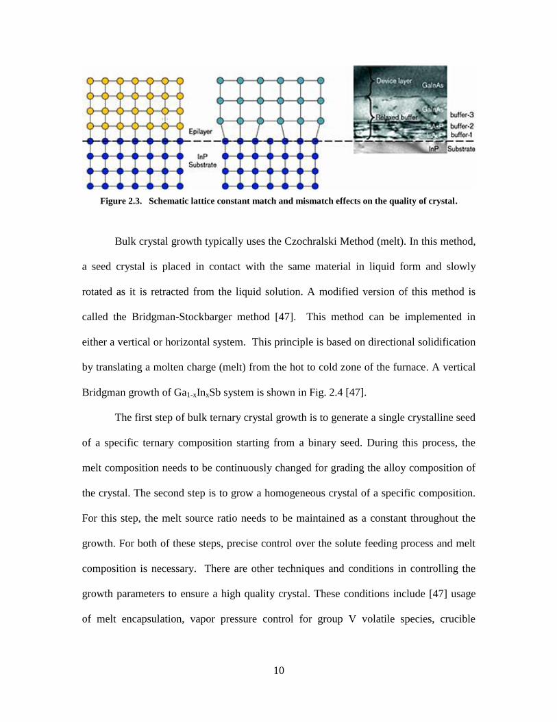
match, stress and defects arise such as dislocations and vacancies as shown in Fig. 2.3
[52, 53]. The strength of stress increases linearly with the epitaxial layer thickness,
limiting the maximum critical thickness that can be grown on a substrate. This is when
the strain energy approaches the chemical energy value. Above this thickness,
dislocations propagate upward, multiplying as they go and forming threading
dislocations, causing adverse effects on the electrical and optical properties.
10
Figure 2.3. Schematic lattice constant match and mismatch effects on the quality of crystal.
Bulk crystal growth typically uses the Czochralski Method (melt). In this method,
a seed crystal is placed in contact with the same material in liquid form and slowly
rotated as it is retracted from the liquid solution. A modified version of this method is
called the Bridgman-Stockbarger method [47]. This method can be implemented in
either a vertical or horizontal system. This principle is based on directional solidification
by translating a molten charge (melt) from the hot to cold zone of the furnace. A vertical
Bridgman growth of Ga1-xInxSb system is shown in Fig. 2.4 [47].
The first step of bulk ternary crystal growth is to generate a single crystalline seed
of a specific ternary composition starting from a binary seed. During this process, the
melt composition needs to be continuously changed for grading the alloy composition of
the crystal. The second step is to grow a homogeneous crystal of a specific composition.
For this step, the melt source ratio needs to be maintained as a constant throughout the
growth. For both of these steps, precise control over the solute feeding process and melt
composition is necessary. There are other techniques and conditions in controlling the
growth parameters to ensure a high quality crystal. These conditions include [47] usage
of melt encapsulation, vapor pressure control for group V volatile species, crucible

11
material, and post growth crystal annealing. Post growth cooling cycles are equally
important. Fast cooling rates can result in thermal strain that results in a cracking of the
wafers during processing.
Figure 2.4. Vertical Bridgman growth of Ga1-xInxSb system.
2.3 Band Structure and Bandgap Energy
Band theory of solids can be used to better understand how crystal structure and
residing defects can affect the fundamental properties of a semiconductor. The simplest
theory in solid state physics is the free electron model. This model is based on the
assumption that conduction band electrons are free to move around. However, they are
confined in semiconductor lattice structures (i.e. the periodic potential which arises from the
lattice arrangement of the host atoms). Using the classical quantum mechanics “particle in a
box” model, one can solve Schrödinger’s equation in the crystal lattice, and the solution of
the wave function gives discrete electronic energy levels [54]. Extending this simplified
model to an infinite number of lattice structures (similar to infinite number of quantum wells
12
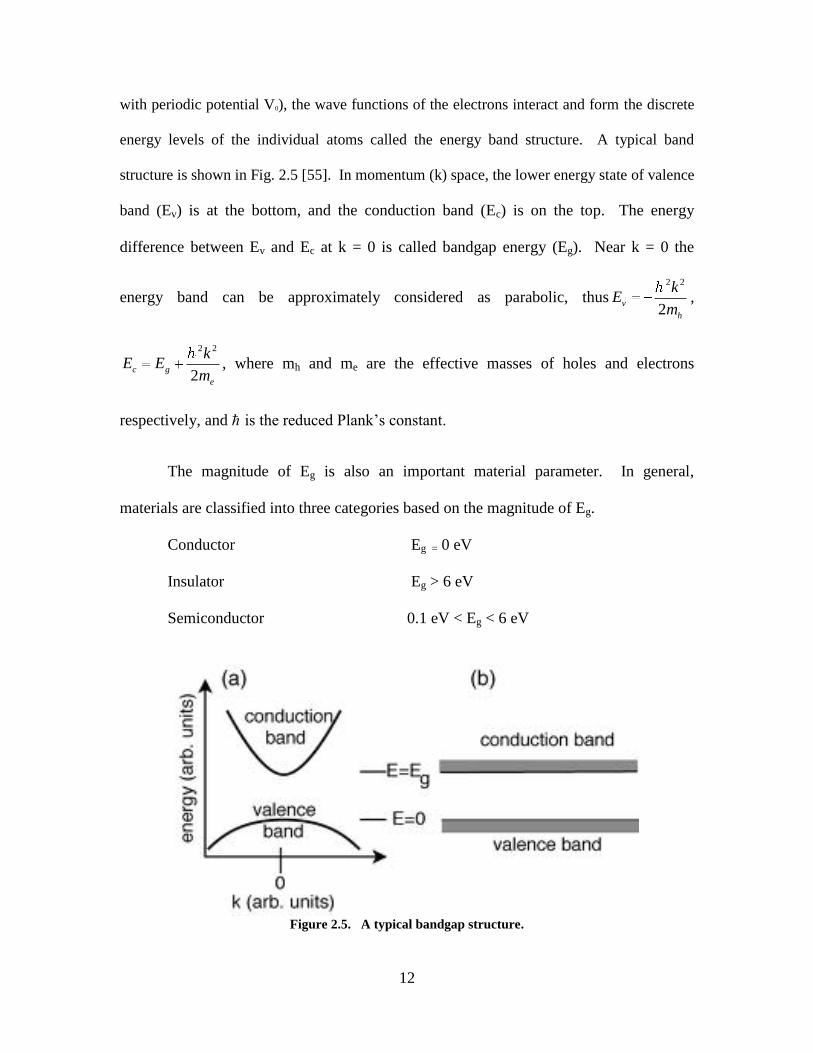
with periodic potential V0), the wave functions of the electrons interact and form the discrete
energy levels of the individual atoms called the energy band structure. A typical band
structure is shown in Fig. 2.5 [55]. In momentum (k) space, the lower energy state of valence
band (Ev) is at the bottom, and the conduction band (Ec) is on the top. The energy
difference between Ev and Ec at k = 0 is called bandgap energy (Eg). Near k = 0 the
energy band can be approximately considered as parabolic, thus2 2
2v
h
kE
m,
2 2
2c g
e
kE E
m, where mh and me are the effective masses of holes and electrons
respectively, and is the reduced Plank’s constant.
The magnitude of Eg is also an important material parameter. In general,
materials are classified into three categories based on the magnitude of Eg.
Conductor Eg = 0 eV
Insulator Eg > 6 eV
Semiconductor 0.1 eV < Eg < 6 eV
Figure 2.5. A typical bandgap structure.

13
Semiconductors act like an insulator at low temperatures. However, as the temperature
increases, a significant number of electrons are thermally excited from the states near the
top of the valence band to those near the bottom of the lowest empty conduction band
because the width of the forbidden energy gap is smaller. This creates partially filled
bands and allows conduction to occur. In general, semiconductor’s Eg is less than ~4 eV.
Throughout this work, investigation is limited to infrared semiconductors, i.e.,
Eg < 1.5 eV.
The density of electrons in the upper band, Nc, (or holes in the lower band, Nh) is
closely related to the Fermi-Dirac distribution,
Tk
EEEf
B
Fexp1
1)( . (2.1)
Here f(E) is the probability of occupying energy states, kB is Boltzmann constant, and T is
the temperature (K). EF is the Fermi energy, which usually lies in the middle of the
bandgap for intrinsic semiconductors. The density of states, gc, at the conduction band is
expressed as
3/2
2 3
(2 )( )
2
ec c
mg E E E , (2.2)
where E > Eg, and me is the effective mass of the upper conduction band electron. Ec is
the energy at the bottom of the conduction band. Below the bandgap energy, where
E<Eg, the density of state is proportional to following relationship:

14
( ) ,
g
B
E E
k Tg E e (2.3)
where T is the temperature and kB is the Boltzmann constant.
Motion of electrons is only allowed in the valance and conduction bands. When a
semiconductor is under optical radiation, if the photon energy is less than the
semiconductor’s bandgap energy, the photon will pass through so that light transmits
through the semiconductor. When the photon energy is larger than the bandgap energy,
this photon will be absorbed by the semiconductor where it excites an electron from the
valance band to its conduction band, leaving behind a positively charged state. Actually
the absence of the electron is referred to as a hole. The hole is not an actual particle, but it
behaves as one and has many similar properties of the electron.
According to Beer-Lamber’s law, the radiation will exponentially decay after
propagating through a media. This relationship can be expressed as
,0
deI
IT (2.4)
where I0 is the incident photon intensity, and I is the transmitted intensity. T is the
transmission (%), is the absorption coefficient of the material, and d is the thickness of
the sample.
For direct bandgap materials, the valance band maximum and conduction band
minimum occur at the same point in k-space as shown in Fig. 2.6 [46]. For an indirect
bandgap material, the Ev maximum and the Ec minimum do not occur at the same point in
k-space. Therefore, for an optical transition, it would require additional conservation of
momentum of phonon besides the energy requirement. Because of this, direct bandgap

15
material such as InAs, GaAs, InP, InGaAs and InAsP are more desirable in making fast
and efficient light sources. On the other hand, some indirect bandgap materials such as
Si, Ge, and diamond are good photo detector candidates.
Full Band Structures
Direct Indirect
Smallest gap at k = 0 Smallest gap NOT at k = 0
Figure 2.6. Illustration of band structures of semiconductor materials.
2.4 Temperature Effects on Semiconductors
At temperature T = 0 K, electrons occupy their lowest energy state. The valance
band is full but the conduction band is completely empty. As the temperature is
increased, some electrons will gain sufficient thermal energy to move to the conduction
band and contribute to conduction. As the temperature further increases, the lattice of the
semiconductor material expands and the oscillations of the atoms near their equilibrium
location in the lattice will increase. This change would narrow the bandgap by changing
16
the population of electrons and holes in the conduction band and the valence band. In
addition, the increased motion of the atoms broadens the energy levels.
This temperature change results in a change of the material properties. For
instance, at temperatures much lower than the Debye temperature, the energy gap varies
proportionately to the square of the temperature. When the temperature is much above
the Debye temperature, the energy gap varies linearly with the temperature. The observed
temperature dependent Eg agrees with the empirical Varshni relationship [56]:
,)0()(2
T
TETE gg
(2.5)
where Eg (0) is the value of the energy gap at 0 K, also called the absolute bandgap
energy, and and are constants (Varshni coefficients). Note that the value of is in
the range of the Debye temperature, but these two coefficients are not independent.
Temperature dependent refractive index is affected by the change of bandgap
energy [57] through the relation
2
0 0
6 1 1,
(4 )
e
g p g g
mdn eg
dE E n E E (2.6)
wherexxx
xxxxxg
11
11211Re
4)(
2, me is the electron mass, n0 is the
refractive index at room temperature and Ep is the Kane energy.

17
For infrared materials,
e
c
g
p
m
m
EE
4
3 , where c
e
m
mis effective electron mass (mc is the
reduced mass). Ep is almost a constant for narrow banggap material, and roughly
Ep=11.24 eV for InAs.
Using the chain rule, one can write:
dT
dE
dE
dn
dT
dn g
g
. (2.7)
Thus, the temperature dependent refractive index can be obtained from the known
temperature dependent bandgap energy and dn/dEg.
2.5 Semiconductor Impurities
A perfect crystal is something that only exists conceptually and can rarely be
found in nature. Semiconductors form closed valance shells through covalent bonding
with their nearest neighbors. When impure atoms from neighboring columns in the
periodic table occupy a lattice site in the host crystal, they attempt to form all the bonds
the crystal's atoms would have created. Sometimes the impure atoms will complete all
the bonds and have one or more extra electrons, such as the case when silicon ions
(column IV) replace Ga (column III) atoms in an InAsP crystal. These “extra” electrons
are then free to modify the conduction. In this case, impurity ions are referred to as
donors. On the other hand, impurity ions may not have enough electrons to complete all
the bonds (e.g., Zn on an As site) and thus create holes that are readily available to
participate in the conduction in the valance band. Impurity ions of this type are called

18
acceptors. The existence of impurities and the impurity level in semiconductor will
greatly affect both the semiconductor’s electrical and optical properties.
When the impure atom is embedded with the pure semiconductor, the binding
energy is significantly reduced. The binding energy of an electron in an impure atom is
much smaller compared to the bandgap. This makes it easier to thermally ionize the
donor electrons to produce conduction. For a semiconductor’s electrical properties, if the
impurities exist in a controlled manner, then the electrical conductivity ( ) can be
manipulated in an accurate and reliable way, which is governed through equation 2.8.
)( pn pne . (2.8)
Where e is the charge of the electron, n and p are the electron and hole carrier
concentrations, andn
and p represent the mobility for the electrons and holes,
respectively. Intentionally introduced impurities can benefit the conduction up to the
critical doping density, at which the doping density becomes so large that the impure
atoms are separated by less than the Bohr radius. At this point the material acts like a
metal.
Heavy doping can result in impure band formation and cause band tailing or band
filling. Spatial distribution of impure atoms is generally random, causing random
fluctuations at the band edges (known as band tailing). As the impurity concentration
grows, free carriers begin to occupy states above the bottom of the conduction band.
This is known as band filling.

19
3. Characterization Techniques and Experimental Setups
In this work, both electrical and optical properties of infrared semiconductor
materials were investigated using various characterization techniques. The detailed
characterization methods and experiments are described in this chapter.
The optical characterizations were performed in the infrared materials Laboratory
at Wright-Patterson Air Force Base (WPAFB) in Ohio. Electrical characterizations were
performed in the Semiconductor Laboratory of the Engineering Physics Department, Air
force Institute of Technology, Bldg 644 at WPAFB.
3.1 Electrical Characterization
The electrical characterization is based on the Hall-effect/sheet-resistivity
measurement. This method provides quantitative information for semiconductor
conductivity type (n- or p-type), carrier concentration, mobility, and resistivity. These
parameters are very useful in semiconductor device designs and applications.
3.1.1 Hall-effect Theory
The Hall-effect theory was discovered in 1879 by Edwin H. Hall, an American
physicist. He discovered that a small transverse voltage was generated across a thin
metal strip in the presence of an orthogonal magnetic field. The discovery of this
transverse voltage (the Hall Voltage) enabled the independent calculation of the mobility
and the carrier concentration of the material, which was only accomplished up to that
time through difficult measurements. In 1958, van der Pauw developed a theory which
could be shown experimentally in an easier manner than the original Hall-effect method.
He showed that the shape of the measuring sample was not a factor and only required that

20
the sample be simply connected and exhibit highly ohmic point contacts on the periphery
of the material [58]. Similar discussions can also be found in Moore’s dissertation [59].
According to the Hall-effect theory, electrons moving in a specimen find
themselves subject to the Lorentz Force in the presence of a perpendicular magnetic field.
Hall-effect measurements are conducted by placing a sample in a magnetic field that is
orthogonal to its surface as illustrated in Fig. 3.1. For the van der Pauw method, a
current is applied to the material so that the charged carriers move in the x direction. The
moving charges induce an internal electric field in the material, which deflects the
charges toward the edges of the material. Positively charged particles (holes) move to
one edge, and the negatively charged particles (electrons) move to the opposite edge.
This particle movement is the result of the charge carriers being subject to the Lorentz
Force, which is normal to the magnetic field. The Lorentz Force is given by
LF q E v B , (3.1)
where q is the charge of the particle, E is the electric field, v is the velocity of the
electrons, and B is the magnetic field. If one type of carrier is dominant, this shift causes
a buildup of unequal surface charge which creates a potential difference across the
sample surface, the Hall voltage.

21
Figure 3.1. A schematic diagram illustrating of the van der Pauw Hall-effect.
This generated transverse voltage will therefore have a different sign for n and p-type
materials as shown in Fig. 3.1.
The Hall-effect can be described much more easily with the rod-shaped specimen,
and the following description applies to rod-shaped specimen. Solving the cross product
in equation 3.1, the Lorentz Force equation becomes
zxyy BqvqEF . (3.2)
The system will strive for equilibrium and therefore the Hall Voltage will grow until it
becomes equal to the Lorentz Force. When this occurs, yF is zero and equation 3.2 can
be simplified to
zxy BvE . (3.3)

22
The current density which is defined in equation 3.4 can be solved for the velocity and
substituted into the electric field equation 3.3, rendering the equation to experimentally
measurable quantities.
Hxx rnqvI H
xx
nqr
Iv . (3.4)
The Hall factor is represented by Hr and denotes the Hall to drift mobility ratio, which is
usually approximated to be 1, but can vary between 1 and 2. This estimation causes Hall
Effect measurements to often underestimate the values of the carrier concentrations. The
substitution of x into equation 3.3 yields an equation for the transverse electric field in
terms of the Hall coefficient, RH, applied current density, Jx, and applied magnetic field,
Bz. That is, it is given by
zxH
H
zxy BJR
nqr
BIE . (3.5)
The above equation is then used to define the Hall voltage, VH. The Hall voltage is the
product of the generated electric field and the width of the sample, w.
wBJRwEV zxHyH . (3.6)
The Hall voltage, being a measurable quantity, is used to calculate the Hall coefficient.
Equation 3.6 can be solved Hall coefficient
wBJ
VR
zx
HH . (3.7)

23
The magnitude of the Hall voltage is inversely proportional to the carrier concentration
and the sign of this voltage indicates the dominant carrier type. For electron
conductivity, the Hall coefficient is negative, and the coefficient is positive for hole
conduction. The sheet carrier concentration, Ns, and mobility, H can be calculated using
following relations:
H
Hs
qR
rN and
s
HH
R. (3.8)
Temperature-dependent Hall (TDH) measurements provide carrier concentrations
and mobility values as a function of temperature. At low temperatures, even the shallow
impurities could freeze, leaving the material highly resistive. If the material is highly
degenerate, TDH measurements will reveal the degenerate layer at low temperatures via
the temperature independent mobility and carrier concentration.
3.1.2 Hall-effect Measurement System
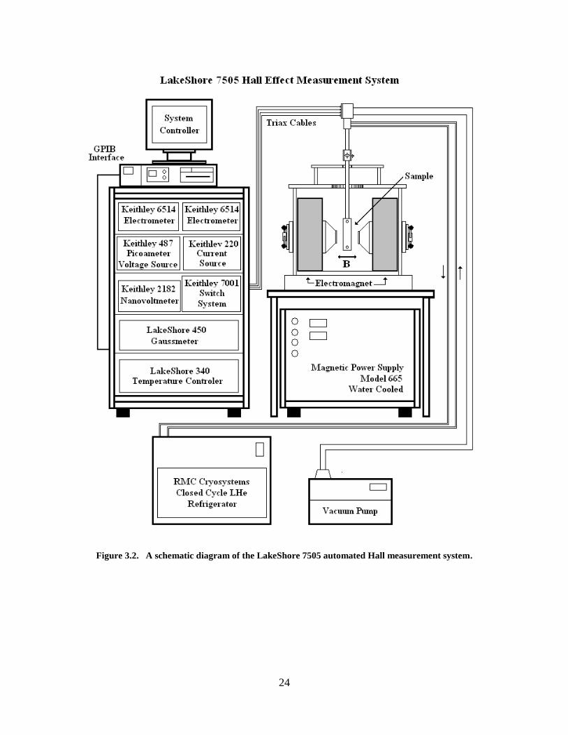
The Hall-effect measurements are made with an automated Lake Shore 7505
system using the standard van der Pauw method. A diagram of the system is provided in
Fig. 3.2. The samples are placed on Janis vacuum heads designed for low (10-320 K)
and high temperature (300-700 K) measurements which are placed between two coil
magnets that are capable of producing up to a 5 kG magnetic field. All measurement is
done in a 5 kG field. Current is supplied to the sample with a Keithley 220 current
source and the generated Hall voltage is measured using a Keithley 2182 nanovoltmeter.
Lake Shore Hall program version 3.3 automates the process and records the resistivity
and Hall data.
24
Figure 3.2. A schematic diagram of the LakeShore 7505 automated Hall measurement system.
25
Hall Measurements provide only average carrier concentration and mobility
values over the entire conducting thickness. A total of 8 current-voltage pair
measurements are averaged to calculate the sheet resistivity. Four current-voltage pair
measurements are taken under forward and reverse magnetic fields, and are averaged to
calculate the Hall coefficient. Temperature-dependent Hall-effect measurements were
made at 5 kG using the standard van der Pauw technique at temperatures ranging from 10
to 300 K. Ohmic contacts were placed on the periphery of the sample using indium.
3.2 Optical Characterization
There are three methods used primarily for optical characterizations in this study.
They are transmission spectrum, photoluminescence (PL), and refractive index
measurements. Other methods such as infrared imagery and micro probe wavelength
dispersing methods were also employed in this study. Optical measurements were
conducted as functions of temperature and sample composition.
3.2.1 Fourier Transform Infrared Spectroscopy
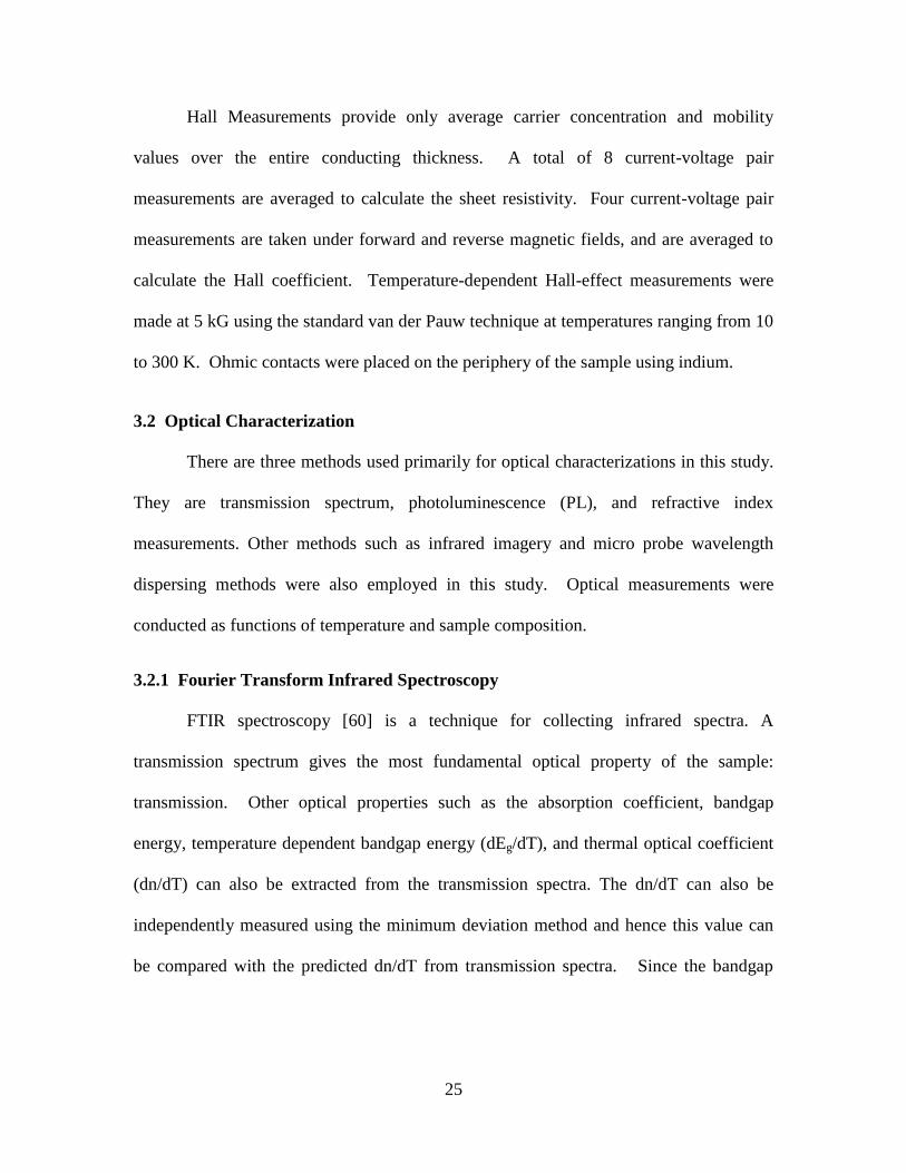
FTIR spectroscopy [60] is a technique for collecting infrared spectra. A
transmission spectrum gives the most fundamental optical property of the sample:
transmission. Other optical properties such as the absorption coefficient, bandgap
energy, temperature dependent bandgap energy (dEg/dT), and thermal optical coefficient
(dn/dT) can also be extracted from the transmission spectra. The dn/dT can also be
independently measured using the minimum deviation method and hence this value can
be compared with the predicted dn/dT from transmission spectra. Since the bandgap

26
energy can also be extracted from the PL measurement, the value can be compared with
that obtained from the transmission spectrum.
A Perkin Elmer Spectrum GX was used to measure the transmission spectra of the
samples. The Perkin Elmer Spectrum GX is a single-beam Michelson interferometer-
based FTIR spectrometer, and was allowed in transmission mode. The system is
configured with a mid-infrared (MIR) or near-infrared (NIR) single source. Most
frequently for InGaAs and InAsP samples, MIR source and MIR beam splitters were
selected. Deuterated Triglycine Sulfate (DTGS) detector allowed for a detection range of
7000 to 50 cm-1
with a maximum resolution of 0.3 cm-1
. It is fully automated and
computer controlled. A schematic layout of the NIR mode of Perkin Elmer Spectrum GX
FTIR system is shown in Fig. 3.3. It includes a built-in 35 W tungsten halogen
illuminator, a motorized stage, and a CCD video camera. The heart of the optical design
is the Michelson interferometer shown in Fig. 3.3, which provides the measurement with
stability, reliability and sensitivity. A single scan measurement is fast, because
information of all frequencies is collected simultaneously. In this work, the wavelength
for MIR is ranging from 0.6 to 25 m. Most samples studied were at a temperature range
of 80 – 400 K. Samples are grouped by InxGa1-xAs and InAs1-yPy with different
compositions of x and y.
27
Figure 3.3. A schematic layout of Perkin Elmer Spectrum GX FTIR system with the PC interface.
3.2.2 Photoluminescence Measurement
A semiconductor material will emit photons as well as thermal radiation when it
is radiated with a sufficient energy such as a laser. There are two types of luminescence
that semiconductors exhibit: fluorescence and phosphorescence. Fluorescence is the
emission of photons due to a direct transition from an excited state to a ground state,
while phosphorescence utilizes intermediate transitions so that the luminescence persists
after the excitation source is terminated. Materials that have this type of luminescence
are generally referred to as phosphors [61]. Semiconductors in this study exhibit
fluorescence. Similar discussions on the PL measurement can also be found in Fellow’s
dissertation [62].

28
PL can be a powerful semiconductor characterization tool because it provides
direct observation of the energy levels that exist in the material. This provides an
excellent tool to appraise the quality of a crystal. Luminescence is a combination of
several types of electron-hole pair recombination such as excited state electrons (e) with
ground state holes (h) in semiconductors. The electrons and holes also relax to
equilibrium through a succession of interactions with defect and impurity levels within
the bandgap, and they eventually leads to recombination. The wavelength of the
emitted luminescence is given by Ec
hh = iE - fE , where h is the Plank's
constant, ν is the frequency, c is the speed of light, λ is the wavelength, and E is the
initial energy (iE ) minus the final energy ( fE ) in the transition.
Possible transitions include transitions between the conduction band to the valence band,
and transitions between levels within the bandgap induced by impurities and defects,
such as donor and acceptor levels. The most common radiative transitions are illustrated
in Fig. 3.4.
Luminescence spectra can be collected for all radiative transitions that occur between two
energy levels. They are: the band-to-band transition (a), the free exciton transition (b),
the neutral donor and free hole recombination (c), a free electron transitioning to a neutral
shallow acceptor (d), and the donor-acceptor transitions for shallow (e) and deep states
(f), which are demonstrated in Fig. 3.4.
29
Figure 3.4. Common radiative transitions take place in semiconductors. (a) band-to-band, (b) free
exciton, (c) neutral donor and free hole recombination, (d) a free electron transitioning to a neutral
shallow acceptor, and (e) (f) donor-acceptor transitions for shallow and deep states, respectively.
Among all of the above transitions, the band-to-band (B-B) transition, labeled (a), is
generally dominant at room temperature. The energy of this transition is given by
,gvc EEEh (3.9)
where Ec is the conduction band minimum, Ev is the valence band maximum, and gE is
the energy gap. The free exciton (FX) transition, labeled as (b), is common in pure
semiconductors, and the electron bound to the hole through Coulombic force recombines.
The energy of this transition is the bandgap energy minus the binding energy of the two
particles (electron and hole), and is shown in equation 3.10.
4
2
*
2
q
g rhv E m (3.10)

30
where *
rm is the reduced effective mass of the exciton, q is the charge, and κ is equal to
r4 , where r is the relative dielectric constant. Transition (c) shows the transition from
an electron on a neutral donor recombining with a free hole (D0, h), while transition (d)
illustrates the recombination of a free electron in the conduction band and a hole on a
shallow neutral acceptor (e, A0). The energies for these transitions are given by
adg EEh , , (3.11)
where Ed is a donor energy level and Ea is an acceptor energy level. The last two
transitions in the diagram are extremely important and are the same transition; only the
depths of the acceptor and the donor levels change. They are the donor-acceptor pair
(DAP) transitions, where an electron on a shallow donor recombines with a hole on a
shallow neutral acceptor, or as seen in (f) where an electron in a deep donor recombines
with a hole in the deep acceptor. The energy of this type of transition is given by
r
qEEEh adg
2
, (3.12)
where r is the separation distance between the donor and the acceptor. The last term in
the equation represents the electrostatic energy gained as the transition is complete. The
DAP transitions can have a broad spectrum due to the wide number of assumed discrete
values r. This transition provides a good means for studying the interband transitions that
occur in the semiconductor material. The FX transition dominates at low temperatures for
most pure semiconductor materials exhibiting strong exciton peaks. The DAP peak can
serve as a measure of the compensation level of the material. A material which is fairly
31
compensated may exhibit strong DAP peaks and be fairly resistive with a high level of
shallow donor and acceptor concentrations.
The relative intensity of the transition feature can give insight into the electrical and
structural properties of the semiconductor material. Deep defect levels in the bandgap
region can trap electrons and prohibit luminescence.
3.2.2.1 Photoluminescence Experiment
The PL experiment setup is shown in Fig. 3.5, where the excitation laser is a
Spectra-Physics BeamLok 2085-20 multi-line continuous wave (CW) argon ion laser
with a principle wavelength of 514.5 nm. The laser beam was attenuated using an optical
neutral density (ND) filter, and passed through an optical chopper running at a duty cycle
of approximately 170 Hz. The laser beam size is about 3 mm in diameter, and was
guided by mirrors to the sample surface. Samples were mounted on a cold finger
connected to the Helitran using Crycon thermal grease to create a heat sink.
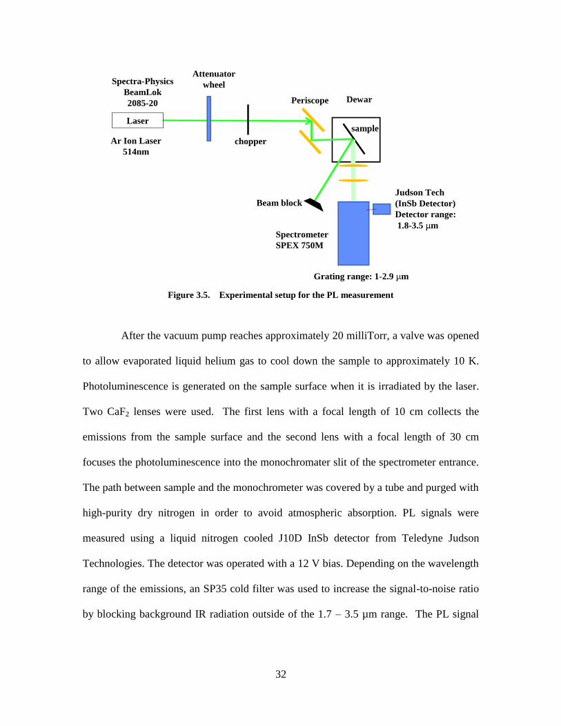
32
Periscope
chopper
Attenuator
wheel
Dewar
sample
Spectrometer
SPEX 750M
Judson Tech
(InSb Detector)
Detector range:
1.8-3.5 m
Spectra-Physics
BeamLok
2085-20
Grating range: 1-2.9 m
Laser
Ar Ion Laser
514nm
Beam block
Figure 3.5. Experimental setup for the PL measurement
After the vacuum pump reaches approximately 20 milliTorr, a valve was opened
to allow evaporated liquid helium gas to cool down the sample to approximately 10 K.
Photoluminescence is generated on the sample surface when it is irradiated by the laser.
Two CaF2 lenses were used. The first lens with a focal length of 10 cm collects the
emissions from the sample surface and the second lens with a focal length of 30 cm
focuses the photoluminescence into the monochromater slit of the spectrometer entrance.
The path between sample and the monochrometer was covered by a tube and purged with
high-purity dry nitrogen in order to avoid atmospheric absorption. PL signals were
measured using a liquid nitrogen cooled J10D InSb detector from Teledyne Judson
Technologies. The detector was operated with a 12 V bias. Depending on the wavelength
range of the emissions, an SP35 cold filter was used to increase the signal-to-noise ratio
by blocking background IR radiation outside of the 1.7 – 3.5 µm range. The PL signal

33
was measured using a Stanford Research SR 850 Lock-In amplifier synchronized to the
optical chopper. These signals were recorded on a computer using SPEX software for
analysis. PL studies were carried out as functions of laser power, sample temperature,
composition and location. The lowest temperature is approximately 10 K, and the highest
temperature reaches 295 K. The laser power range is 100-500 mW. Three to five
locations per sample were investigated. The samples used in these PL studies are listed
in table 3.1.
Table 3.1. List of samples used in the PL experiments and their composition
Sample name of
InxGa1-xAs
Composition
x*
Sample name of
InAs1-yPy
Composition
y*
InAs WT 524-10 1 IAP 040709 0.19
IGA 061206-6 0.99 IAP 101807-11 0.24
IGA 052406-4 0.93 IAP 31407-8 0.34
IGA 052406-2 0.91 IAP 022308 b3 0.41
IGA 052406-1 0.82
IGA 041506-1 0.75
*Composition is measured using CAMECA SX 100 micro probe analyzer at AFRX/RXB, building 655,
area B, WPAFB, Ohio
34
3.3 Refractive Index
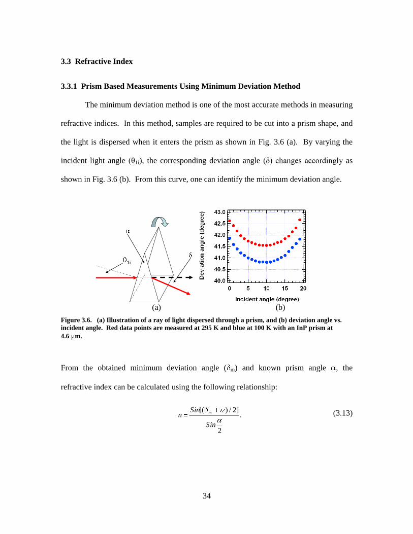
3.3.1 Prism Based Measurements Using Minimum Deviation Method
The minimum deviation method is one of the most accurate methods in measuring
refractive indices. In this method, samples are required to be cut into a prism shape, and
the light is dispersed when it enters the prism as shown in Fig. 3.6 (a). By varying the
incident light angle (θ1i), the corresponding deviation angle (δ) changes accordingly as
shown in Fig. 3.6 (b). From this curve, one can identify the minimum deviation angle.
1i
(a) (b)
Figure 3.6. (a) Illustration of a ray of light dispersed through a prism, and (b) deviation angle vs.
incident angle. Red data points are measured at 295 K and blue at 100 K with an InP prism at
4.6 m.
From the obtained minimum deviation angle ( m) and known prism angle , the
refractive index can be calculated using the following relationship:
.
2
]2/)[(
Sin
Sinn m (3.13)

35
In this minimum deviation method, a prism shaped InAs1-yPy sample is placed in a
cryostat. Sample temperature is controlled by an Omega temperature controller with a
temperature range from 77 K to 300 K. The temperature-dependent refractive index,
n(T), as well as dn/dT can be measured. Several laser sources having wavelengths of
3.39 m, 4.6 m, and 10.6 m are used. The prism has dimensions as shown in Fig. 3.7
(a). The experimental setup for refractive index measurement is shown in Fig. 3.7 (b).
The sample is mounted on a rotational stage having resolution of 0.001 . Distance, d, is
determined by calibration on a reference sample and of CaF2. L is the location where the
detector has the highest intensity for each incident angle. The deviation angle ( ) is given
by tan-1
(L/d).
0.8-10.5
1.3
4
200 angle!!
Laser
Dewar
Linear
polarizer
Half wave
plate
prism
light
Detector
Displacement L
Distance d
C-axis
(a) (b)
Figure 3.7. (a) Prism dimensions; (b) Minimum deviation method experimental layout.
3.3.2 Wafer Based Measurement Using Michelson and Fabry-Perot Interferometer
Both Michelson and Fabry-Perot interferometers were used to measure the optical
path length (OPL) for wafer shaped samples [63-65].
OPL = nd, (3.14)

36
where n is refractive index, d is the sample thickness. Refractive index (n) can be
determined if d is known, and vice versa. However, it is difficult to measure an accurate
thickness at low temperature and thus difficult to determine n at low temperatures. When
combining the two methods (Michelson and Fabry-Perot interferometers), n and d can be
decoupled, enabling determination of n and d precisely at any temperature. The schematic
layout is shown in Fig. 3.8.
sample
laser
detector
BS
reference
mirror
sample
mirror
Figure 3.8. Schematic layout of the Michelson and Fabry Perot interferometers.
A wafer shape sample is placed in a cryostat, which is able to control over a temperature
range of 100 – 295 K. A rotation stage is used to rotate the sample. The optical path
changes as the sample is rotated as shown in Fig. 3.9. That is, the optical length changes
from (L1 + nd + L2) to (L1 + nd'( ) + z'( ) +L2), where is the rotation angle.

37
Sample perpendicular
to incident laser path
Sample oriented at an
angle, , to laser path
Optical path difference = (nd' + z') – nd
dn·d
L1
L2 L2
L1
n·d'
z'dn·d
L1
L2 L2
L1
n·d'
z'
Figure 3.9. Illustration of optical path nd changing with rotating angle
In case of Michelson interferometer, this optical length change in sample arm affects the
intensity reading at a detector, where two electric fields combine. One is the laser beam
reflected from the reference mirror which is a constant, and the other is the laser beam
reflected from the sample mirror, which depends on rotation angle. These combined two
electrical fields at a detector can be expressed as:
2 24exp sin 1 cos exp .D s s r r
i dE A n A i (3.15)
The intensity read by a detector is the modulus square of the electric field, thus the
intensity received by the detector is:
2 2 2 242 cos sin 1 cos .D r s r s s r
i dI A A A A n (3.16)
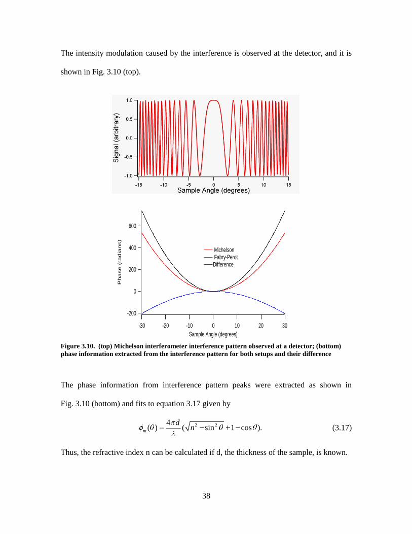
38
The intensity modulation caused by the interference is observed at the detector, and it is
shown in Fig. 3.10 (top).
600
400
200
0
-200
Ph
ase
(ra
dia
ns)
-30 -20 -10 0 10 20 30
Sample Angle (degrees)
Michelson Fabry-PerotDifference
Figure 3.10. (top) Michelson interferometer interference pattern observed at a detector; (bottom)
phase information extracted from the interference pattern for both setups and their difference
The phase information from interference pattern peaks were extracted as shown in
Fig. 3.10 (bottom) and fits to equation 3.17 given by
2 24( ) ( sin 1 cos ).m
dn (3.17)
Thus, the refractive index n can be calculated if d, the thickness of the sample, is known.
39
If the sample thickness is unknown, Fabry-Perot interferometer will be needed.
A simple Fabry-Perot interferometer is formed when the reference mirror in Fig.
3.8 is blocked. Rotating sample results in laser intensity modulations of the transmitted
light due to the interference of multiple internal reflections. Similar to Michelson
interferometry, an interference pattern is received at a detector and the phase information
can be extracted using equation 3.18 given by
2 24( ) ( sin ).fp
dn (3.18)
When combining both Michelson and Fabry-Perot interferometers, the sample thickness
is decoupled as shown in equation 3.19, thus both d and n can be determined.
4( ) ( ) (1 cos ).m fp
d (3.19)
Refractive-index measurements were carried out on bulk InxGa1-xAs wafer
fabricated from a boule grown using multi-zone vertical gradient freeze (VGF) technique.
The sample was placed in a LN2 cooled cryostat. The cold finger was mounted on a
rotation stage with a resolution of ± 0.001o. Two discrete laser sources were used, a
pulsed (kHz) frequency doubled CO2 laser at 4.6 m (2W) and a grating CW CO2 laser at
10.6 m (200 mW). All light sources were chopped at a repetition rate of 50 Hz using a
ThorLabs optical chopper synchronized to a lock-in amplifier. The signal-to-noise ratio
could be increased using lock-in amplifier (SR850). Different beam splitters were used
for each laser source, a dielectric coated CaF2 (50/50) for the 4.6 m laser and a coated
ZnSe (50/50) for the 10.6 m laser. A Boston Electronics HgCdTe photodiode was used
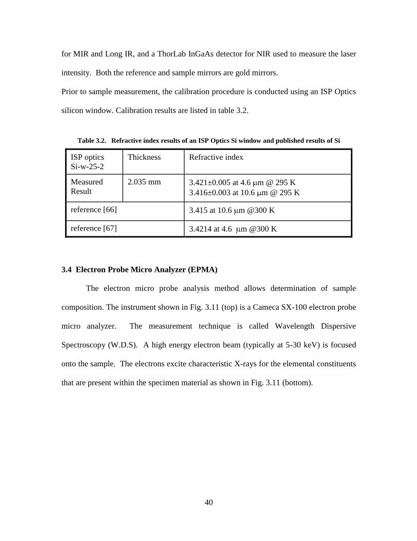
40
for MIR and Long IR, and a ThorLab InGaAs detector for NIR used to measure the laser
intensity. Both the reference and sample mirrors are gold mirrors.
Prior to sample measurement, the calibration procedure is conducted using an ISP Optics
silicon window. Calibration results are listed in table 3.2.
Table 3.2. Refractive index results of an ISP Optics Si window and published results of Si
ISP optics
Si-w-25-2
Thickness Refractive index
Measured
Result
2.035 mm 3.421±0.005 at 4.6 m @ 295 K
3.416±0.003 at 10.6 m @ 295 K
reference [66] 3.415 at 10.6 m @300 K
reference [67] 3.4214 at 4.6 m @300 K
3.4 Electron Probe Micro Analyzer (EPMA)
The electron micro probe analysis method allows determination of sample
composition. The instrument shown in Fig. 3.11 (top) is a Cameca SX-100 electron probe
micro analyzer. The measurement technique is called Wavelength Dispersive
Spectroscopy (W.D.S). A high energy electron beam (typically at 5-30 keV) is focused
onto the sample. The electrons excite characteristic X-rays for the elemental constituents
that are present within the specimen material as shown in Fig. 3.11 (bottom).

41
Figure 3.11. (Top) Electron probe micro analyzer (EPMA): CAMECA 100. (Bottom) a typical
analysis spectrum of EPMA.
The X-ray count rates are then measured on the specimen, and they are compared against
the x-ray count rates collected from the standard reference materials composition. A
matrix correction is then applied to convert the X-ray count rate into concentration values
in weight fraction. In our case, the data was then normalized to 100% total composition
so that the concentrations could be reported as an atomic percentage. The SX-100 uses
the PAP matrix correction in which PAP is a general model for the calculation of X-ray
intensities and can be used for a wide range of X-ray energies (100 eV to greater than 10
keV) and accelerating voltages (1- 40 keV). GaAs, InAs, and InP were used as reference
materials for the calibration of the wavelength dispersive spectrometers for our analyses.
Calibration is always done just prior to analysis.

42
The volume of specimen material analyzed is tear drop shaped having a diameter
on the order of a few microns (5 m) at each analysis point. The size of the analysis
volume varies depending on several factors such as accelerating voltage of the electrons,
average atomic number of the specimen material, and energy of the X-rays being excited.
In this study, each measurement is an average result from 16 sample locations. However,
since this is a micro analyzer, it may have its limit in studying bulk composition of large
area. In this study, two methods (micro analyzer and PL) will be compared in the analysis
of composition.
3.5 Infrared Imagery
Since these samples are optically transparent in the infrared, a Santa Barbara
Focalplane ImagIR infrared camera [68] shown in Fig. 3.12 was used for this study. This
camera uses an InSb focal plane arrays and includes Integrated Detector/Dewar/Cooler
Assemblies, and digital camera heads.
Figure 3.12. Santa Barbara focaplance image IR infrared camera.

43
The imaging system is shown in Fig. 3.13, where sample is placed in front of the
camera. At the far left is a black body source. Next are two lenses to collimate the
blackbody in order to illuminate on the back surface of the sample. The PC is connected
to the integrated InSb detector, and using the WinIR software, the image from the PC can
be saved to a digital disc.
Figure 3.13. MIR imaging system using Santa Barbara Focalplane ImagIR.
Typical IR images obtained from this camera are shown in Fig. 3.14. In these
images, a photodiode (heat source) is placed next to the sample to enhance the visibility.
Six InAs samples of different thicknesses and from different vendors were viewed. From
Fig. 3.14, sample HAFB5_1, IA 03052_1 and IA03052_2 show good optical quality by
their high optical transparency and uniformity. On the other hand, cloudy spots and light
scattering were seen in sample IA 03052_1 and IA 03051_2, indicating defects in these
crystals.
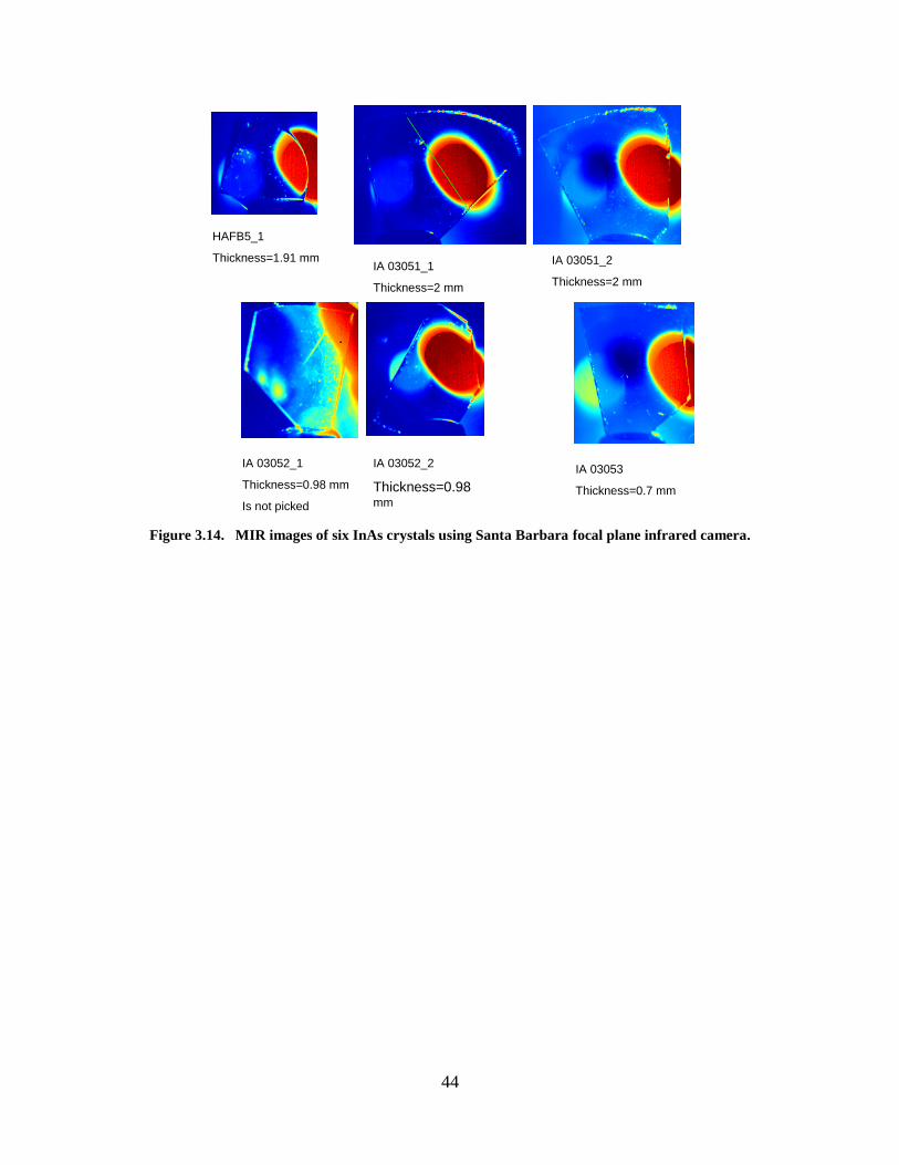
44
HAFB5_1
Thickness=1.91 mmIA 03051_1
Thickness=2 mm
IA 03051_2
Thickness=2 mm
IA 03052_1
Thickness=0.98 mm
Is not picked
IA 03052_2
Thickness=0.98mm
IA 03053
Thickness=0.7 mm
Figure 3.14. MIR images of six InAs crystals using Santa Barbara focal plane infrared camera.

45
4. Results and Discussions of Binary InAs, InP, and GaAs
4.1 Purpose
Studying binary crystals such as InAs, InP and GaAs serves two purposes. First,
they are the end compositions of ternary InxGa1-xAs and InAs1-yPy (x, y =0, or 1).
Therefore, these binaries are natural boundaries of the ternary alloys. Second, binary
(epitaxial layer or bulk) InAs, InP, and GaAs have been extensively studied in the past, so
many electrical and optical properties are known. Thus these binaries can provide
excellent reference points by extrapolating the results obtained from ternary properties as
a function of composition. Moreover, not all the optical properties for binary
compounds are known, for example, at cryogenic temperature or over a wide spectral
range. This work provides the necessary measurements over the extended temperature
and spectral range.
4.2 Determination of Bandgap Energy
PL is a well established method of estimating bandgap energy [69]. The
absorption coefficient ( ) method [70] is another way to determine bandgap energy in
semiconductors. In both cases, they are not always available at all desired temperatures
or spectral ranges. For instance, most PL measurements are carried out at cryogenic
temperatures and the PL peak becomes broad as the temperature increases, disappearing
long before reaching room temperature. As a result, it is difficult to estimate the bandgap
energy at room or higher temperatures using PL. As for the absorption coefficient
method, it is dependent on the absorption edge intersecting the photon energy in the
absorption spectra, which can be complicated by impurities in the semiconductor.

46
Impurities can cause band tailing [71, 72], making it difficult to accurately determine the
bandgap energy. This complication becomes worse when studying newly developed
materials such as melt-grown bulk ternary InxGa1-xAs and InAs1-yPy. Since their crystal
growth condition has yet to be optimized, the current state of ternary crystal quality is far
from being perfect. In other words, impurity and/or defect levels could be high. In the
worst case, PL can be scattered and the PL spectrum may be completely unavailable.
Therefore, the absorption coefficient method must be used to find bandgap energy.
The following sections describe an alternative method of extracting the bandgap
energy directly from the transmission spectra.
The expression for transmission through an etalon is given as:
,1
)1(T
22
2
d
d
eR
eR (4.1)
where T is the transmittance, R is the reflectance, is the absorption coefficient, and d is
the sample (wafer) thickness. At normal incidence, 2
1
1
n
nR , where n is the index of
refraction. For a single pass, transmission at normal incidence is given by
.)1(T 2
0
deRI
I (4.2)
For semiconductors, there are two regions near the bandgap. One of them is
known as the Urbach region [73], where the energy is less than bandgap. Another is
known as the Kane absorption region [74], where the energy is greater than bandgap.
That is, the absorption coefficient can be approximately expressed as
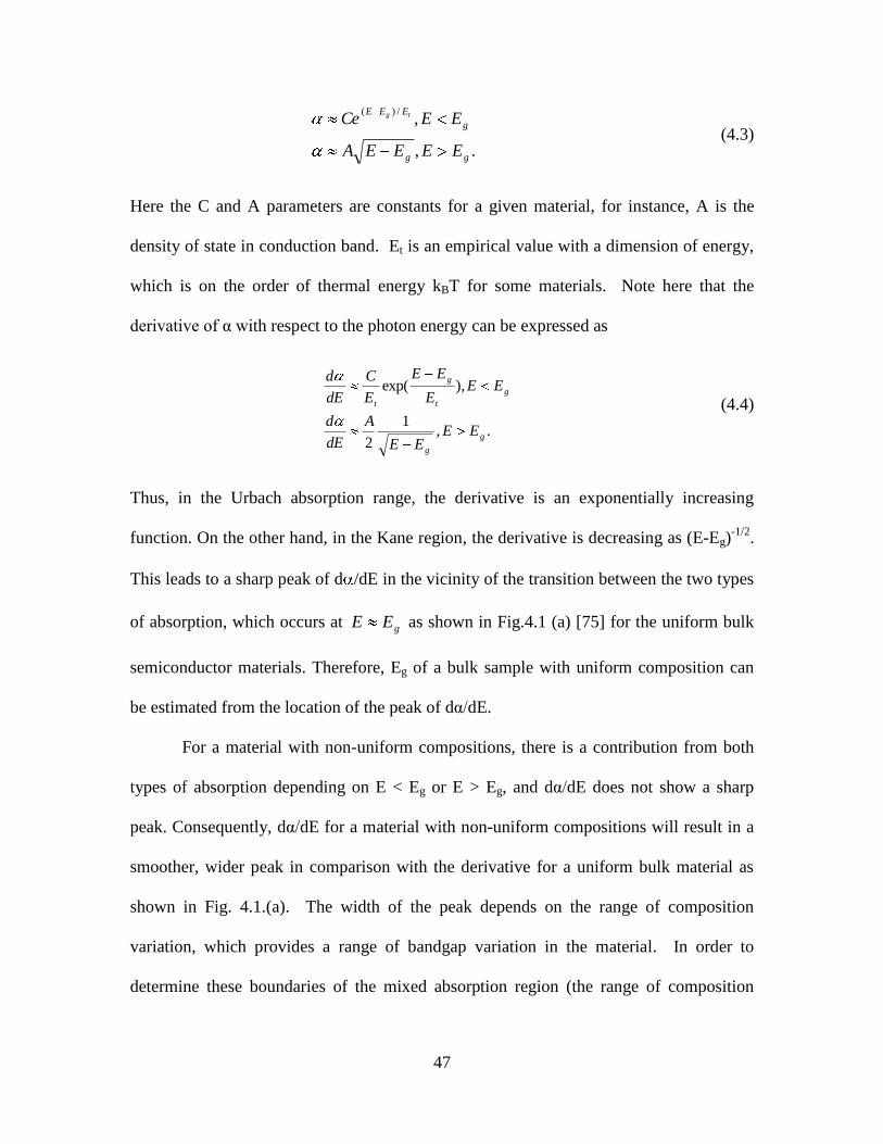
47
.,
,/)(
gg
g
EEE
EEEEA
EECe tg
(4.3)
Here the C and A parameters are constants for a given material, for instance, A is the
density of state in conduction band. Et is an empirical value with a dimension of energy,
which is on the order of thermal energy kBT for some materials. Note here that the
derivative of α with respect to the photon energy can be expressed as
.,1
2
),exp(
g
g
g
t
g
t
EEEE
A
dE
d
EEE
EE
E
C
dE
d
(4.4)
Thus, in the Urbach absorption range, the derivative is an exponentially increasing
function. On the other hand, in the Kane region, the derivative is decreasing as (E-Eg)-1/2
.
This leads to a sharp peak of d /dE in the vicinity of the transition between the two types
of absorption, which occurs at gEE as shown in Fig.4.1 (a) [75] for the uniform bulk
semiconductor materials. Therefore, Eg of a bulk sample with uniform composition can
be estimated from the location of the peak of dα/dE.
For a material with non-uniform compositions, there is a contribution from both
types of absorption depending on E < Eg or E > Eg, and dα/dE does not show a sharp
peak. Consequently, dα/dE for a material with non-uniform compositions will result in a
smoother, wider peak in comparison with the derivative for a uniform bulk material as
shown in Fig. 4.1.(a). The width of the peak depends on the range of composition
variation, which provides a range of bandgap variation in the material. In order to
determine these boundaries of the mixed absorption region (the range of composition

48
variation) more precisely, the second derivative, d2α/dE
2, is obtained as shown in Fig. 4.1
(b) [75], where points of peaks are defined as Eg min and Eg max. The energy difference
ΔEg = Eg max - Eg min can be measured as the distance between the peaks of d2α/dE
2 and
dα/dE. While the derivative peaks (1st and 2
nd) do not indicate the precise numerical value
of the bandgap, this approach appears to be very sensitive to bandgap variations within
the material [75].
an
d d
/dE
(a) (b)
Figure 4.1. (a) A theoretical graph of the absorption coefficient and its first derivative in a uniform
bulk sample showing a sharp peak of the derivative in the vicinity of the bandgap. (b) The second
derivative of the absorption coefficient for different values of bandgap variation within the sample.
4.2.1 Bandgap Energy Obtained from Transmission Spectra for InAs
Our modified method is based on Ariel’s model [75]. It begins with taking the
first and second derivatives of transmission (equation 2.4) instead of the absorption
coefficient with respect to the photon energy. After some rearrangement, the first and
second derivatives of transmission are as follows.
'T
TdedE
dd
dE
d d (4.5)

49
2 22
2 2
TT [ ( ) ]
d d dd d
dE dE dE (4.6)
Transmission spectra of a set of InAs 143 samples with different thickness were
measured at room temperature and the results are shown in Fig. 4.2. (a). These wafers
were grown by the Wafer Technology Company, and diced and thinned by United
Semiconductor LLC into seven pieces with thicknesses ranging from 100 – 1000 m.
EL min and EL max can be determined from the peak locations of dE
dT and 2
2T
dE
d as shown
in Fig. 4.2 (b) and (c), respectively. They have similar characteristics of the Eg min and
Eg max shown in Fig. 4.1(a) and (b). The difference is that EL min and EL max shown in
Fig. 4.2 (b) and (c) are sample thickness dependent, whereas the Eg min and Eg max are not.

50
Figure 4.2. (a) Transmission spectra of InAs 143 samples with five thicknesses (b) d(-T)/dE vs. E.
Peak locations are defined as EL min. (c) d2(-T)/dE
2 vs. E. The minimum locations are defined as
EL max. E is photon energy.
(a)
(b)
(c)

51
The values of EL min and EL max energies in eV were extracted from the peak locations of
dE
dT and 2
2T
dE
d , respectively and the results are plotted as a function of thickness in
Fig. 4.3. Difference between EL min and EL max is in the range of 5 – 10 meV for each
sample and both data are fit to exponential function as shown in equations 4.7 and 4.8.
EL min = 0.326 + 0.032 exp(- d/164) (4.7)
EL max = 0.329 + 0.028 exp(- d/341), (4.8)
where d is the sample thickness in m.
Figure 4.3. EL min and EL max vs. sample thickness for a set of InAs 143 samples
From equations 4.7 and 4.8, EL min(d=0) =0.358 eV and EL max(d=0) =0.357 eV, which
agree very well with the published InAs bandgap values, that are in the range of
0.354~0.36 eV at room temperature, [69, 76-77]. Thus, 0max0min dLdLg EEE .

52
Another observation from Fig. 4.3 is that EL min decreases faster than EL max as sample
thickness increases from 0 to 600 m, and then EL min almost remains constant after
d > 800 m. For InAs, this also reveals that for a thick sample (d ≥ 1 mm), the difference
between bandgap energy and EL, (Eg -EL min) or (Eg - EL max), is about 32 and 28 meV,
respectively.
4.3 Temperature Dependent Bandgap Energy Obtained from Transmission Spectra
Temperature dependent bandgap energy is valuable information for
semiconductor material, but it is not available for many ternary materials such as InGaAs
and InAsP. If the temperature dependent bandgap energy can somehow be extracted
directly from the transmission spectra, it would be very useful, because the knowledge of
temperature dependent bandgap energy gdE
dT
is essential for device designers as well as
field engineers. In addition, the temperature dependent refractive index (dn/dT), known
as the thermo optical coefficient, is another important parameter that can be calculated
from gdE
dT
[47].
In order to find Eg/dT, we like to start with taking second derivatives of the
absorption coefficient

53
g
E
EE
t
EEeE
C
dE
dt
g
,22
2
, (4.9)
,,)(4
2
3
2
2
gg EEEEA
dE
d (4.10)
where *2
2
3
**
**2 2
e
eh
eh
mnch
mm
mmq
A is a constant for a given material [78,79]. From equation 4.6,
and 4.9, it can be found that
g
t
g
t
t
g
EEE
EEdC
E
E
EEdC
],1exp[
expT
"T2
(4.11)
The peak location of (T’), which is EL min, can be found by solving equations 4.11 for
T”=0. Then,
gtLg EEdCEEE ),ln(min (4.12)
Here, EL min can be found from transmission data. Et is a function of temperature.
4.3.1 Temperature Dependent Bandgap of InAs
Temperature dependent transmission spectra of an InAs sample WT 524-10
having a thickness of 1 mm is shown in Fig. 4.4 (top), and its dE
dT are plotted as a
function of photon energy in Fig. 4.4 (bottom).

54
Figure 4.4. (Top) Temperature dependent transmission spectra of InAs sample WT 524-10.
(Bottom) temperature dependent dE
dT plotted as a function of photon energy
The values of EL min (red dots) are extracted from the peak locations of dE
dT from
Fig. 4.4 (bottom). Then the EL min (red dot) are plotted as a function of temperature as
shown in Fig. 4.5, along with the published bandgap of InAs by Fang et al. [69] (solid
curve).
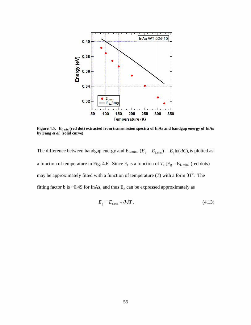
55
Figure 4.5. EL min (red dot) extracted from transmission spectra of InAs and bandgap energy of InAs
by Fang et al. (solid curve)
The difference between bandgap energy and EL min, )( minLg EE = ),ln(dCEtis plotted as
a function of temperature in Fig. 4.6. Since Et is a function of T, [Eg – EL min] (red dots)
may be approximately fitted with a function of temperature (T) with a form Tb. The
fitting factor b is ~0.49 for InAs, and thus Eg can be expressed approximately as
,min TEE Lg (4.13)
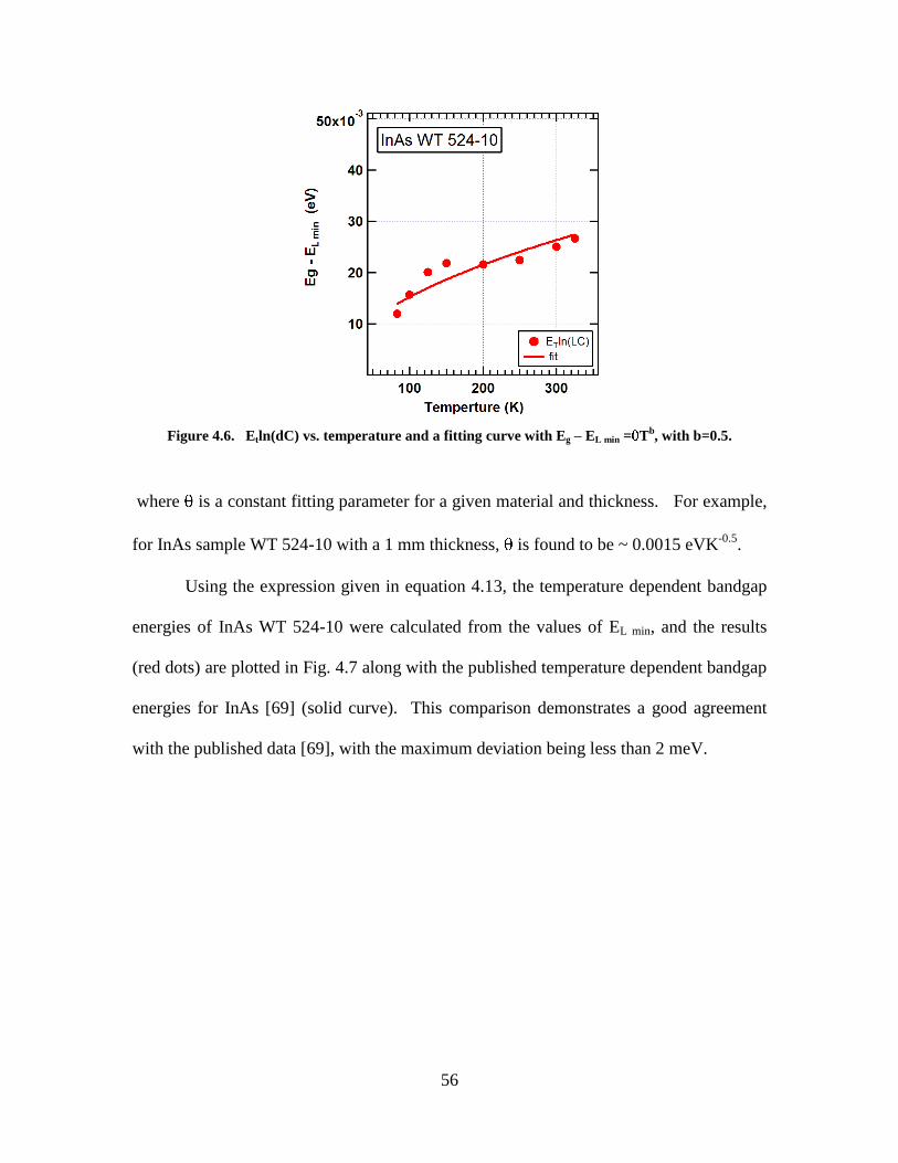
56
Figure 4.6. Etln(dC) vs. temperature and a fitting curve with Eg – EL min = Tb, with b=0.5.
where is a constant fitting parameter for a given material and thickness. For example,
for InAs sample WT 524-10 with a 1 mm thickness, is found to be ~ 0.0015 eVK-0.5
.
Using the expression given in equation 4.13, the temperature dependent bandgap
energies of InAs WT 524-10 were calculated from the values of EL min, and the results
(red dots) are plotted in Fig. 4.7 along with the published temperature dependent bandgap
energies for InAs [69] (solid curve). This comparison demonstrates a good agreement
with the published data [69], with the maximum deviation being less than 2 meV.
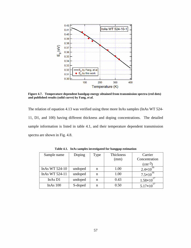
57
Figure 4.7. Temperature dependent bandgap energy obtained from transmission spectra (red dots)
and published results (solid curve) by Fang, et al.
The relation of equation 4.13 was verified using three more InAs samples (InAs WT 524-
11, D1, and 100) having different thickness and doping concentrations. The detailed
sample information is listed in table 4.1, and their temperature dependent transmission
spectra are shown in Fig. 4.8.
Table 4.1. InAs samples investigated for banggap estimation
Sample name Doping Type Thickness
(mm)
Carrier
Concentration
(cm-3)
InAs WT 524-10 undoped n 1.00 2.4×10¹⁶
InAs WT 524-11 undoped n 1.00 7.5×10¹⁶
InAs D1 undoped n 0.43 1.58×10¹⁷
InAs 100 S-doped n 0.50 5.17×10¹⁷

58
Figure 4.8. Temperature dependent transmission spectra of three InAs samples (a) InAs WT 524-11
(b) InAs D1 (c) InAs 100.
(a)
(b)
(c)
n=1.6×10¹⁷
cm-3
n=7.5×10¹⁶
cm-3
n=5.2×10¹⁷
cm-3
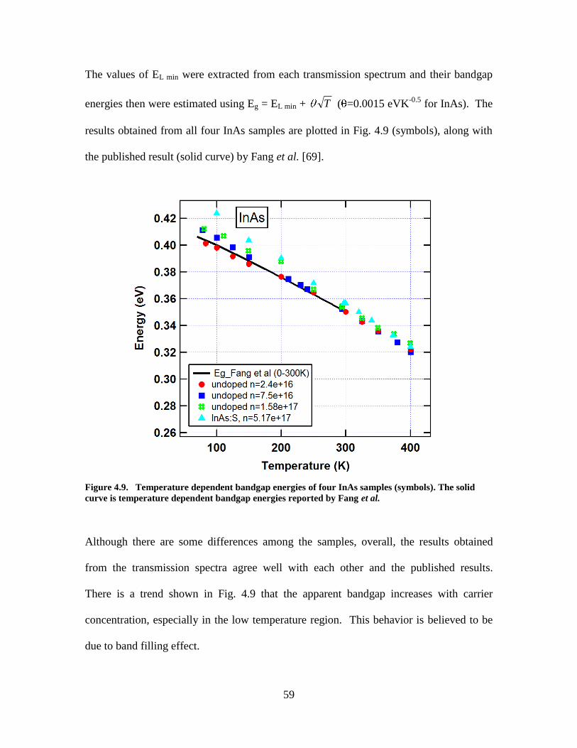
59
The values of EL min were extracted from each transmission spectrum and their bandgap
energies then were estimated using Eg = EL min + T ( =0.0015 eVK-0.5
for InAs). The
results obtained from all four InAs samples are plotted in Fig. 4.9 (symbols), along with
the published result (solid curve) by Fang et al. [69].
Figure 4.9. Temperature dependent bandgap energies of four InAs samples (symbols). The solid
curve is temperature dependent bandgap energies reported by Fang et al.
Although there are some differences among the samples, overall, the results obtained
from the transmission spectra agree well with each other and the published results.
There is a trend shown in Fig. 4.9 that the apparent bandgap increases with carrier
concentration, especially in the low temperature region. This behavior is believed to be
due to band filling effect.

60
4.3.2 Temperature Dependent Bandgap of InP
Three InP samples investigated and their detailed sample information are listed in
table 4.2.
Table 4.2. InP Sample Information
Sample name Doping Type Thickness (mm) Carrier
Concentration
(cm-3
)
InP R 3781 un_7 undoped n 1.00 4.02×10¹⁷
InP 6 undoped p 0.96 1.56×10¹⁸
InP B_2 undoped n 1.00 2.47×10¹⁸
Temperature dependent transmission spectra of these three InP samples are shown
in Fig. 4.10.

61
Figure 4.10. Temperature dependent transmission spectra of three InP samples (a) InP B2 (b) InP
R3781 un (c) InP 6.
(a)
1 mm thick
n = 2.47×10¹⁸
cm-3
(b)
1 mm thick
n = 4.00×10¹⁷
cm-3
(c)
0.96 mm thick
p = 1.56×10¹⁸
cm-3

62
Fig. 4.11 shows two graphs of (dE
dT ) vs. photon energy for InP sample B2 and
R3781 un, respectively. Sample InP 6 display similar characteristic curves as that of B2
and R3881 un, and it is not shown here. EL min values were extracted from the peak
locations of (dE
dT ) for all InP samples, and were plotted in Fig. 4.12 (top) (symbols),
along with the published Eg results (solid curve) [76]. The differences between Eg and EL
min were plotted in Fig. 4.12 (bottom), and were fitted with equation 4.13. For these InP,
the obtained value is 0.0036 eVK-0.5
.
(a) (b)
Figure 4.11. dE
d T)1(vs. E for InP sample at various temperatures (a) InP sample B2. (b) InP sample
R3781_un.
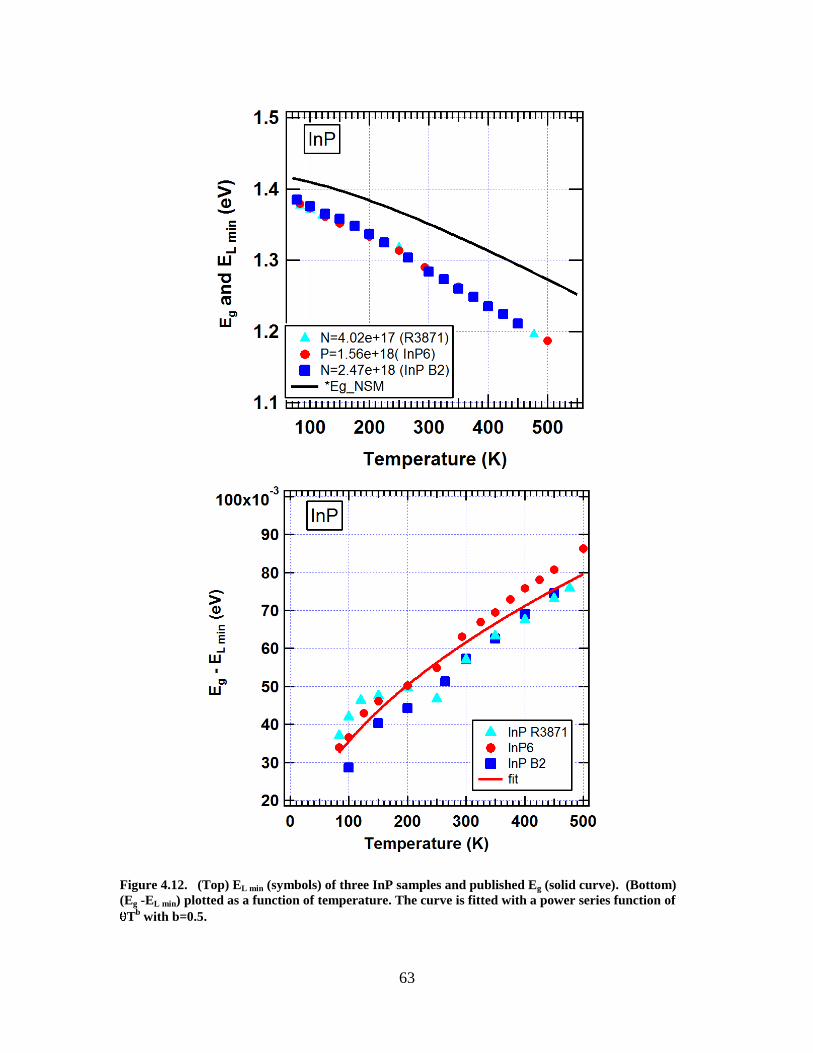
63
Figure 4.12. (Top) EL min (symbols) of three InP samples and published Eg (solid curve). (Bottom)
(Eg -EL min) plotted as a function of temperature. The curve is fitted with a power series function of
Tb with b=0.5.

64
Bandgap of InP as a function of temperature was calculated using equation 4.13 with
known and EL min and the results are shown in Fig. 4.13. The published bandgap
energies of InP [76] calculated using equation 4.14 are also plotted in this figure.
).8000(327
109.4421.1)(
4
TT
TEg (4.14)
The results obtained from transmission data demonstrate good agreement with the
published values, and the average deviation is ~2 meV. It is interesting to point out that
the bandgap energy of InP is less dependent on its carrier concentration than that of InAs.
This could be because InAs has much narrower bandgap energy (0.354 eV) than InP
(1.412 eV). When impurities are doped into the material, the doping affects band filling
more for narrow than for wide bandgap materials.
Figure 4.13. Temperature dependent bandgap energies obtained from transmission spectra (triangle,
dot, and square) for three InP samples and published bandgap energies (solid curve).

65
4.3.3 Temperature Dependent Bandgap of GaAs
Transmission spectra were measured for several GaAs samples and they are listed
in table 4.3. These are intrinsic samples and their exact carrier concentrations are not
available.
Table 4.3. GaAs sample information
Sample name Vendor Thickness (mm)
GaAs 82 unknown 0.31
GaAs 19557 Wafer Tech 0.50
GaAs 12472-24 Wafer Tech 0.62
Temperature dependent transmission spectra of three GaAs samples are shown in
Fig. 4.14 along with a dE
dT plot as a function of photon energy for GaAs sample
12472-24. The dE
dT plots of other two GaAs samples display similar characteristic
curves as that of the GaAs sample12472-24, and they are not shown here.

66
(a) (b)
( c ) (d)
Figure 4.14. (a), (b) and (c) Temperature dependent transmission spectra of three GaAs samples of
GaAs 82, GaAs WV 19557 and GaAs 12472-24, respectively. (d) d(1-T)/dE of GaAs 12472-24 plotted
as a function of photon energy.
EL min values of all three GaAs samples were extracted from the peak locations of dE
dT ,
and were plotted in Fig. 4.15 (a) (symbols) along with the published Eg values (solid
curve) [76] that were calculated using the following equation 4.15.
204
10405.5519.1)(
4
TTEg (0 < T < 1000) (4.15)

67
(a) (b)
Figure 4.15. (a) Extracted EL min of three GaAs samples (symbols) and published Eg values (solid
curve). (b) Temperature dependent bandgap energies of three GaAs samples obtained from
transmission spectra (#, dot, and square) and published Eg values (solid curve).
The differences between the published bandgap energies and EL min of GaAs were
curve fitted with a power series function of Tb with b=0.5, and the obtained value was
0.0023 eVK-0.5
. Eg was then calculated using equation 4.13 and the results were shown in
Fig. 4.15 (b) along with the published data (solid curve). They exhibit good agreement in
all temperature range and the maximum deviation is less than 3 meV.
The obtained values of InAs, GaAs and InP were plotted as a function of
refractive index in Fig. 4.16. It seems that is inversely proportional to the refractive
index, which is a purely empirical observation with no physical explanation so far.
Further verification is needed to see whether this relationship will hold more generally
for other III-V semiconductors such as GaN, GaP, GaSb and InSb or not.
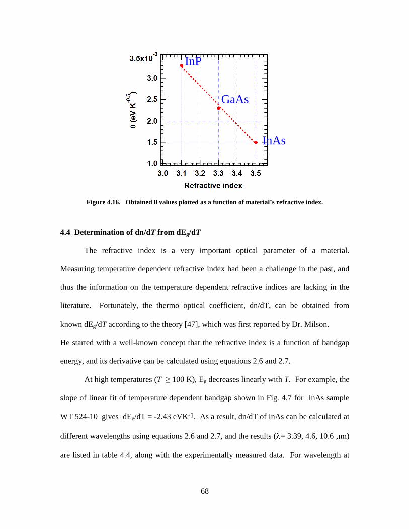
68
InAs
GaAs
InP
Figure 4.16. Obtained values plotted as a function of material’s refractive index.
4.4 Determination of dn/dT from dEg/dT
The refractive index is a very important optical parameter of a material.
Measuring temperature dependent refractive index had been a challenge in the past, and
thus the information on the temperature dependent refractive indices are lacking in the
literature. Fortunately, the thermo optical coefficient, dn/dT, can be obtained from
known dEg/dT according to the theory [47], which was first reported by Dr. Milson.
He started with a well-known concept that the refractive index is a function of bandgap
energy, and its derivative can be calculated using equations 2.6 and 2.7.
At high temperatures (T ≥ 100 K), Eg decreases linearly with T. For example, the
slope of linear fit of temperature dependent bandgap shown in Fig. 4.7 for InAs sample
WT 524-10 gives dEg/dT = -2.43 eVK-1. As a result, dn/dT of InAs can be calculated at
different wavelengths using equations 2.6 and 2.7, and the results ( = 3.39, 4.6, 10.6 m)
are listed in table 4.4, along with the experimentally measured data. For wavelength at

69
4.64 m, there is a good agreement within an accuracy of 1.6% between the predicted
dn/dT ( 2.58×10⁻⁴ K-1) and the directly measured dn/dT (2.54×10⁻⁴ K-1).
Table 4.4. Comparison between calculated dn/dT and measured dn/dT
( m)
dn/dEg
(eV-1)
dEg/dT
(×10-4, eVK-1)
Calc. dn/dT
(×10-4,K-1)
Measured
dn/dT
(×10-4, K-1)
3.39 -1.43 -2.43 3.48 2.55
4.64 -1.06 -2.43 2.58 2.54
10.6 -0.64 -2.43 1.45 1.96
4.5 Refractive-Index Measurements
The prism angle is measured using the setup shown in Fig 4.17. A red HeNe laser
was aligned perpendicular to the prism. A photo diode detector with a 25 m pinhole
aperture was mounted next to the HeNe laser. The distance between detector and the
prism was about 65 cm, which gives an accuracy of the prism angle measurement to
1.3x10⁻³
degree. To measure the prism angle, first, the initial angle is defined by adjusting
the laser beam reflected from the prism as the maximum intensity at the detector location.
Then the prism is rotated until the HeNe laser is reflected back from another side of the
prism surface to obtain the maximum intensity at the detector position. The prism angle
= absolute value of (180 ± the rotation angle), where + or – is dependent on the rotation
direction.
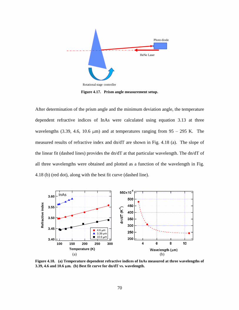
70
HeNe Laser
Rotational stage controller
Photo diode
Figure 4.17. Prism angle measurement setup.
After determination of the prism angle and the minimum deviation angle, the temperature
dependent refractive indices of InAs were calculated using equation 3.13 at three
wavelengths (3.39, 4.6, 10.6 m) and at temperatures ranging from 95 – 295 K. The
measured results of refractive index and dn/dT are shown in Fig. 4.18 (a). The slope of
the linear fit (dashed lines) provides the dn/dT at that particular wavelength. The dn/dT of
all three wavelengths were obtained and plotted as a function of the wavelength in Fig.
4.18 (b) (red dot), along with the best fit curve (dashed line).
3.60
3.55
3.50
3.45
3.40
Re
fra
cti
ve
in
de
x
300250200150100
Temperature (K)
4.6 m
3.39 m
10.6 m
InAs
(a) (b)
Figure 4.18. (a) Temperature dependent refractive indices of InAs measured at three wavelengths of
3.39, 4.6 and 10.6 m. (b) Best fit curve for dn/dT vs. wavelength.

71
Similarly, the temperature dependent refractive indices of InP at four wavelengths
(1.55, 3.39, 4.64 and 10.6 m) were measured and the results are shown in Fig. 4.19 (a) .
The slope of the linear fit (dashed line) provides the thermal optical parameter (dn/dT) of
InP, and was plotted as a function of wavelength in Fig. 4.19 (b) along with a best fit
curve.
(a) (b)
Figure 4.19. (a) Temperature dependent refractive index of InP measured at four wavelengths of
1.55, 3.39, 4.6 and 10.6 m. (b) Best fit curve for dn/dT vs. wavelength.
Similar to InAs, the theoretical value of dn/dT can be calculated using equations
2.6 and 2.7. Assuming
e
c
g
p
m
m
EE
4
3 , Ep ~12.66 eV can be obtained for InP. The
temperature dependent bandgap energy for InP was evaluated in section 4.3, and at high
temperatures ( T >100 K), dEg/dT =-2.88×10⁻⁴
eVK-1
. Also dn/dEg was calculated using
equation 2.7. Using these values, dn/dT at different wavelengths were obtained and
listed in table 4.7 along with the experimentally measured results. From table 4.7, one
can see that the calculated dn/dT does not agree well with the experimental results. This

72
is probably due to inaccurate dn/dEg. The relationship
e
c
g
p
m
m
EE
4
3 , is probably valid only
for narrow bandgap material such as InAs (0.354 eV), and may not be valid for wide
bandgap semiconductors such as InP (1.35 eV).
Table 4.5. Comparison between calculated dn/dT and experimental dn/dT
( m)
dn/dEg
(eV-1)
dEg/dT
(×10-4, eVK-1)
Calc. dn/dT
(×10-4,K-1)
Exp. dn/dT
(×10-4, K-1)
1.55 -0.18 -2.88 0.52 2.01
3.39 -0.18 -2.88 0.52 1.48
4.64 -0.18 -2.88 0.51 1.36
10.6 -0.17 -2.88 0.50 1.10

73
5. Results and Discussions on Bulk Ternary InAs1-yPy
Undoped Bulk ternary InAs1-yPy (IAP) polycrystals with diameters up to 50 mm
were grown from pseudo-binary InP-InAs melt using the vertical Bridgman technique by
United Semiconductor Ltd (USL). In this chapter, InAs1-yPy and its electrical and optical
properties are discussed as functions of phosphorus mole fraction and sample
temperature. Some of the results were published in [80].
The first section of this chapter begins with a brief introduction regarding
InAs1-yPy crystal growth followed by information on the samples used in this
investigation. In section two, several visualization techniques are employed to
characterize the crystal. From section three and on, discussions will focus on some
fundamental yet very important optical and electrical properties of InAs1-yPy crystals.
5.1 Ternary InAs1-y Py Crystal Growth
Undoped melt-grown bulk InAs1-yPy (0<y<1) polycrystals were grown using the
vertical Bridgman technique at United Semiconductor LLC by Geeta Rajapopalan. Here a
description of her growth technique is provided for reference.
The compound synthesis and growth were controlled in sealed silica crucibles using
pre-synthesized binaries of undoped InP and InAs. Growth temperatures and melt
compositions were selected from the pseudo-binary InP-InAs phase diagram reported in the
literature [41]. In order to grow a compositionally uniform InAs1-yPy (along the growth
direction), excess InP was placed at the top of the melt to provide solute replenishment
during crystal growth. First, pre-synthesized polycrystalline ingots of binary InP and InAs
were placed inside a flat bottom silica crucible, and the crucible was then evacuated to a

74
vacuum level of approximately 10-6 torr and sealed. No seeds were used in any of the crystal
growths. The sealed crucibles were placed inside the uniform temperature zone of the
furnace and heated to melt the InAs ingot placed at the bottom of the crucible. The furnace
was further slowly heated to the growth temperature (approximately 2-3 oC higher than the
liquidus temperature for the desired alloy composition). The InAs acted as the solvent to
partially dissolve the InP ingot and form the InAs1-yPy melt. Some portion of the InP ingot
remained undissolved and served as the solute replenishment source during the crystal
growth process. After the solute dissolution step, the crucible was slowly translated through
the temperature gradient of the furnace to implement directional solidification. Typical
growth rates were in the range of 0.5-1.0 mm/hr. The entire melt was allowed to solidify
and then the grown crystal was cooled to room temperature at a rate of 50 oC/hr. Due to
the melt replenishment by the InP feed at the top of the melt, the grown crystals were fairly
compositionally homogeneous along the growth direction except at the last two freeze
regions. The crystals were also reasonably homogeneous in composition along the radial
direction.
A typical crystal boul is shown in Fig. 5.1 (a), which was then sliced by a
diamond blade saw to a wafer shown in Fig. 5.1 (b). The surfaces of the wafers were
ground using 14 µm boron carbide or silicon carbide abrasives followed by chemo-
mechanical polishing using 1 µm and 0.5 µm alumina abrasive slurries. After the final
polishing step, high optical quality mirror shining surfaces were obtained. The optical
quality of this sample, shown in Fig. 5.1 (c), was imaged using a Santa Barbara
Focalplane ImagIR MIR infrared camera. In this picture, the camera was focused on the

75
ruler placed immediately behind the wafer. Except for some localized dark spots, this
figure clearly indicates good infrared optical transmission over the entire wafer.
(a) (b) (c)
Figure 5.1. (a) Crystal boul, (b) crystal wafer, and (c) MIR image of an InAs1-yPy crystal.
Six InAs1-yPy crystal bouls were grown with a different phosphorus mole fraction,
ranging from 0.19 – 0.66 by USL in 2009. Then, each boul was used to fabricate a
25 mm wafer, a square sample with dimensions of 15x15x1 mm, and a right angle
prism with prism angle approximately equal to 20o. The prism shape and dimensions are
shown in Fig. 5.2. Usually, the circle wafer sample is designed for the PL and a
transmission measurement, the square shape sample is designed for the Hall-effect
measurement, and the prism is designed for the refractive index measurement. In order to
maintain consistency, whenever possible, the same square shape sample was used for PL,
transmission, and Hall-effect measurements. The sample names and their compositions
are listed in table 5.1. The phosphorus mole fraction compositions were measured using
the Cameca SX-100 electron probe micro analyzer. Each composition value was
obtained from an average of 16 measurement points, each point covering an approximate
~5 m2 area.

76
Table 5.1. Bulk ternary InAs1-yPy sample information
Name 040709B6 040709B3 032009B7 032009B3 020409B7 020409B3
y 0.193
± 0.008
0.337
± 0.005
0.441
± 0.005
0.541
± 0.004
0.586
± 0.005
0.659
± 0.002
Figure 5.2. Prism used in refractive index measurements using minimum deviation method.
5.2 Bulk InAs1-x Py Crystal Images
Bandgap energy of InAs1-yPy varies from 0.36 to 1.35 eV, corresponding to a
cutoff wavelength ( c) from 3.44 to 0.92 µm. The MIR Santa Barbara focal plane
infrared camera wavelength range is from 3 to 5 m, which is suitable for full
composition range studies for InAs1-yPy. The IR images of studied samples are shown in
Fig. 5.3.
(a) (b) (c) (d) (e) (f)
y= 0.19 0.34 0.44 0.54 0.59 0.66
Figure 5.3. MIR images of InAs1-yPy crystal samples.

77
One can immediately make an initial assessment regarding the crystal’s quality by
looking at the images shown in Fig. 5.3. For instance, samples (a) and (d) are better
optical quality crystals then samples (b) and (c), while samples (e) and (f) show poor
optical quality. The optical transmission is a very important property for materials used
in optical devices. Poor optical transmission could be due to impurity scattering, crystal
defects, as well as inhomogeneity in crystal composition. These negative factors can not
only reduce optical transmission, but can also cause serious problems such as phase
distortion and reduce the device’s efficiency.
By imaging a laser source after passing through a sample, one is able to compare
how the sample affects the light (spatial profile). The following investigation is
conducted using a pulsed (kHz), frequency doubled Coherent DEOS CO2 laser with a
wavelength of 4.6 m and maximum power of 2 W. A PyrocamTM
III pyroelectric array
camera (made by Spiricon Inc.) was used. The recorded images are shown in Fig. 5.4.
The first image is the laser beam only, which was imaged without passing through a
sample. The second image is the laser beam after passing through an InAs1-yPy crystal
with y=0, which is actually a binary crystal (InAs). Therefore, the laser beam quality is
unchanged and remains a Gaussian-like beam after passing through the sample, indicating
this sample is a high quality crystal. However, as y increases in value, the laser beam
quality decreases gradually as shown in Fig. 5.4 (bottom). When the laser beam passes
through the sample with y > 0.53, it scatters and completely loses its Gaussian beam shape.
Finally, when y=1 (InP), the laser beam shape is restored and once again it becomes
Gaussian-like. This finding is consistent with what we have learned from previous chapters:
it is very difficult to grow good quality ternary bulk crystal. This also reveals that it is more
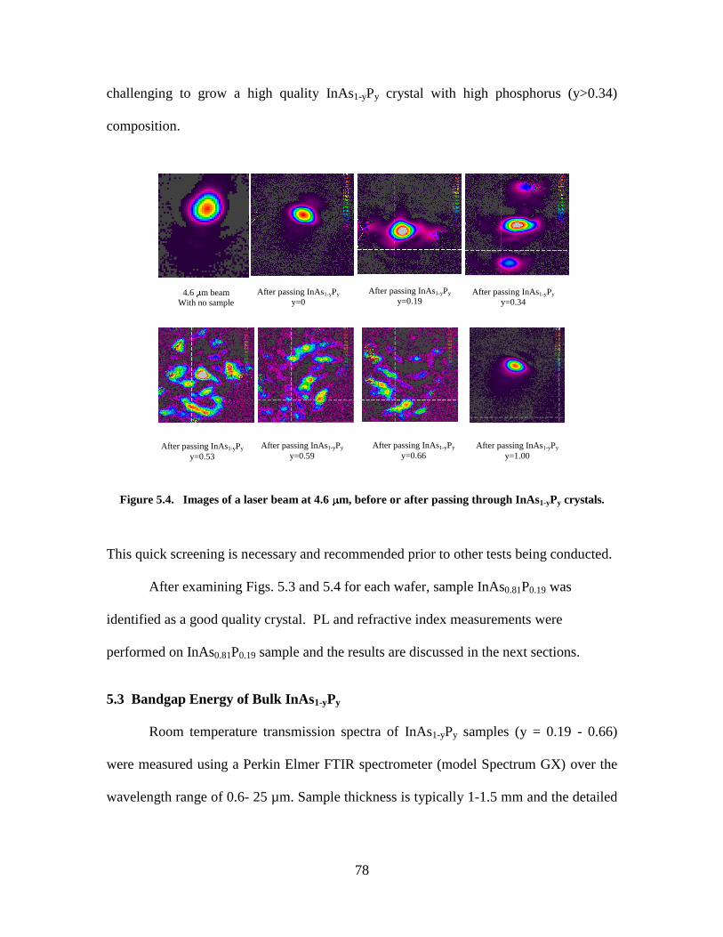
78
challenging to grow a high quality InAs1-yPy crystal with high phosphorus (y>0.34)
composition.
4.6 m beam
With no sample
After passing InAs1-yPy
y=0
After passing InAs1-yPy
y=0.19 After passing InAs1-yPy
y=0.34
After passing InAs1-yPy
y=0.59
After passing InAs1-yPy
y=0.66
After passing InAs1-yPy
y=1.00 After passing InAs1-yPy
y=0.53
Figure 5.4. Images of a laser beam at 4.6 m, before or after passing through InAs1-yPy crystals.
This quick screening is necessary and recommended prior to other tests being conducted.
After examining Figs. 5.3 and 5.4 for each wafer, sample InAs0.81P0.19 was
identified as a good quality crystal. PL and refractive index measurements were
performed on InAs0.81P0.19 sample and the results are discussed in the next sections.
5.3 Bandgap Energy of Bulk InAs1-yPy
Room temperature transmission spectra of InAs1-yPy samples (y = 0.19 - 0.66)
were measured using a Perkin Elmer FTIR spectrometer (model Spectrum GX) over the
wavelength range of 0.6- 25 µm. Sample thickness is typically 1-1.5 mm and the detailed

79
composition information is listed in table 5.1. From the transmission spectra shown in
Fig. 5.5 (top), each sample has reasonably well defined cutoff wavelength for each
phosphorus mole fraction. For a thin film InAs1-yPy, the bandgap energy at room
temperature was reported [81] as a function of phosphorus mole fraction as
Eg (y) = 0.356 + 0.675y +0.32y2. (5.1)
Bandgap energies of bulk InAs1-yPy crystals to date have not been reported in the
literature. In order to obtain the bandgap energy of a bulk InAs1-yPy sample as a function
of phosphorus mole fraction, y, directly from the transmission spectra, derivatives of
transmission spectra with respect to photon energy were plotted as a function of photon
energy as shown in Fig. 5.5 (bottom), from which the EL min, the peak location of dT/dE ,
was extracted. This method was explained in details in section 4.5.

80
Figure 5.5. (Top) Transmission spectra of six InAs1-yPy samples with composition ranging from 0.19
to 0.66; (bottom) the 1st derivatives of transmission spectra with respect to photon energy plotted as
a function of photon energy.
The obtained EL min values were plotted as a function of composition in Fig. 5.6 (red
dots), along with the bandgap values calculated from thin film results (black solid line)
using equation 5.1. The EL min values generally follow well with the bandgap energies
(Eg) that were estimated for the thin epitaxial layers [81].

81
Figure 5.6. EL min values obtained from transmission spectra (red dots), were plotted as a function of
phosphorus composition. The solid line is the bandgap energies of InAs1-yPy calculated from
equation 5.1.
Obviously, there are some differences between Eg and EL min as shown in Fig. 5.6. For
example, the EL min at y=0.19 is slightly below the Eg, on the other hand, the EL min at
y= 0.59 is slightly above the Eg. The difference is about 26 meV. This discrepancy is
most likely due to material inhomogeneity and also partly due to the difference between
Eg and EL min. Photoluminescence measurement results in the following section will
provide further explanations.
5.4 Photoluminescence Measurements
The PL spectra of InAs0.81P0.19 taken at 10 K with a laser excitation power of
100 mW at different sample locations are shown in Fig. 5.7. Five selected locations on
the InAs0.81P0.19 sample are indicated on top right in Fig. 5.7.

82
ED
C
B
A
Figure 5.7. Location dependent PL spectra of an InAs0.81P0.19 sample taken at 12 K with a laser
excitation power of 300 mW.
83
PL peak positions are clearly dependent on the sample position indicating sample
nonuniformity. This shows high sensitivity of PL measurement. Normalized PL spectra
mainly consist of two peaks which are attributed to the free exciton (FX) and donor-
acceptor pair (DAP) transitions. The FX peak locations shown in Fig. 5.7 are 0.556,
0.575, and 0.594 eV, showing a variation of 38 meV. These PL results indicate a
compositional variation of approximately 4.8% across the sample, which is about 6×
larger than the findings listed in table 5.1 from a micro probe analyzer. This composition
variation within the sample may explain some of the discrepancies between EL min and Eg
observed in Fig. 5.6.
Power dependent PL spectra were also measured at 12 K for the InAs0.81P0.19
sample, and the results are shown in Fig. 5.8. At a lower power level (at or below
200 mW), the dominant PL peak is at 0.540 eV (indicated as B in Fig. 5.8). As the
excitation power is increased to above 200 mW, the peak A becomes gradually dominant.
These excitation power-dependent PL results can be used to identify the origin of the
transition because the relationship between the integrated PL peak intensity and the laser
excitation power is dependent on the nature of the PL transition [82]. A linear
relationship between the excitation power and the integrated PL intensity indicates an
excitonic recombination; a sub-linear relationship indicates a defect or impurity related
transition, and a quadratic dependence indicates a band-to-band transition [83, 84].

84
Figure 5.8. Photoluminescence spectra of InAs0.81P0.19 sample measured at 12 K with different
incident laser powers.
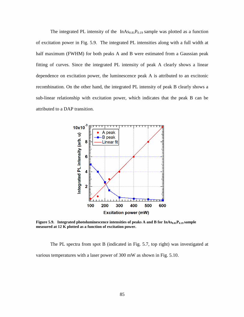
85
The integrated PL intensity of the InAs0.81P0.19 sample was plotted as a function
of excitation power in Fig. 5.9. The integrated PL intensities along with a full width at
half maximum (FWHM) for both peaks A and B were estimated from a Gaussian peak
fitting of curves. Since the integrated PL intensity of peak A clearly shows a linear
dependence on excitation power, the luminescence peak A is attributed to an excitonic
recombination. On the other hand, the integrated PL intensity of peak B clearly shows a
sub-linear relationship with excitation power, which indicates that the peak B can be
attributed to a DAP transition.
Figure 5.9. Integrated photoluminescence intensities of peaks A and B for InAs0.81P0.19 sample
measured at 12 K plotted as a function of excitation power.
The PL spectra from spot B (indicated in Fig. 5.7, top right) was investigated at
various temperatures with a laser power of 300 mW as shown in Fig. 5.10.

86
Figure 5.10. Temperature dependent PL spectra of the InAs0.81P0.19 with a laser power of 300 mW.

87
The donor to acceptor pair transition peak at 0.540 eV was observed at 12 K, but this
peak disappeared after the temperature was raised greater than 30 K. The FX peak red-
shifts when the temperature increases. This is due to bandgap shrinkage by the crystal
lattice expansion and the increase in lattice vibration in the crystal. The FX peak
positions are red-shifted by approximately 40 meV as the temperature is increased from
12 to 130 K.
The FX peak energies (red data points) versus temperature for the InAs0.81P0.19
sample are shown in Fig. 5.11 along with the EL min (black squares) obtained from the
transmission spectra. They seem to follow each other very well, indicating similar
temperature dependencies. Since the free exciton binding energy is assumed to be very
small (InP is ~3.5 meV, GaAs is ~ 1.5 meV, and InAs is ~1.3 meV.) [69, 85], FX can be
approximately considered as the bandgap energy. However, the existing inhomogeneity
in the sample greatly complicates the problem. Note that these FX peaks were taken at
the sample location B (shown in Fig. 5.7), where the FX peak value is smaller than other
locations in the sample. The variation in energy between locations B and D is about
24 meV, and between locations B and E is ~37 meV.
On the other hand, EL min should always be below the bandgap. From the
discussion in section 4.5, for a 1 mm thick InAs, the difference between Eg and EL min at
room temperature is ~30 meV, and is ~57 meV for InP.
At room temperature, the composition dependent bandgap energy of ternary
InAs1-yPy thin film is mostely known [81]. If bulk InAs1-yPy has the same bandgap energy
as that of the thin film, the bandgap of InAs1-yPy at y=0.19 can be calculated using

88
equation 5.1. Since the difference (Eg – EL min) was found to be 22 meV.
TEE Lg min , and = 0.00125 eVK-0.5
is obtained.
The temperature dependent Eg then can be calculated from EL min as shown in
Fig. 5.11 (blue triangles). The obtained Eg value are curve fitted using the Varshni’s
equation (equation 2.5), the results are shown in Fig.5.12 as a solid curve. The empirical
Varshni coefficients for InAs0.81P0.19 sample are found to be Eg (0) = 0.564 eV,
=0.450 meV/K, and = 300 K.
Figure 5.11. FX peak of InAs0.81P0.19 (red) and ELmin (black) vs. Temperature. Eg (blue) is calculated
using equation TEE Lg min.

89
Figure 5.12. FX peak (red dots) and EL min (black) of InAs0.81P0.19 vs. Temperature. Eg is calculated
using Eq. TEE Lg min (blue), and the Varshni equation is a solid black line.
Several other InAs1-yPy samples with different compositions were also studied. Their
temperature dependent bandgap energies were obtained using temperature dependent PL
and transmission spectra but are not shown here. Composition dependent Varshni
coefficients were obtained and they are summarized in table 5.2.

90
Table 5.2. Summary of composition dependent Varshni coefficients for InAs1-yPy
Composition
y
Eg(0) (×10-4
)
eV/K (K)
dEg/dT from linear fit
×10-4
(eVK-1
)
0.00 0.415 2.76 83 -2.4314
0.19 0.564 4.50 300 -2.7482
0.24 0.611 5.09 300 -3.1085
0.34 0.704 5.19 300 -3.1696
1.00 1.421 4.90 327 -2.8788
Results of temperature dependent bandgap energy of InAs1-yPy are plotted as a function
of temperature in Fig. 5.13.
Figure 5.13. Temperature dependent bandgap energy of InAs1-yPy .

91
5.5 Refractive Index Measurements
The refractive index of the InAs0.81P0.19 crystal was measured as functions of
wavelength and temperature, and the results are plotted in Fig. 5.14. At all three
wavelengths, the refractive index varied linearly in the temperature range between 90 K
and 295 K according to the following relationships:
n at 3.39 µm = 3.3193 + 2.13x10⁻⁴
T,
n at 4.64 µm = 3.3106 + 1.94x10⁻⁴
T,
n at 10.6 µm = 3.2844 + 1.81x10⁻⁴
T.
Fig. 5.15 shows the wavelength dependent refractive indices for InAs0.81P0.19 measured at
various temperatures. The dashed lines are curve-fitted at each temperature for different
photon wavelengths (λ) using the Cauchy equation,
42
)()()(),(
TCTBTATn . (5.2)
The estimated values of Cauchy coefficients, A(T), B(T), and C(T) are listed in table 5.3
for the InAs0.81P0.19 alloy, along with the measured values for the binary InAs (y=0) and
InP (y=1).
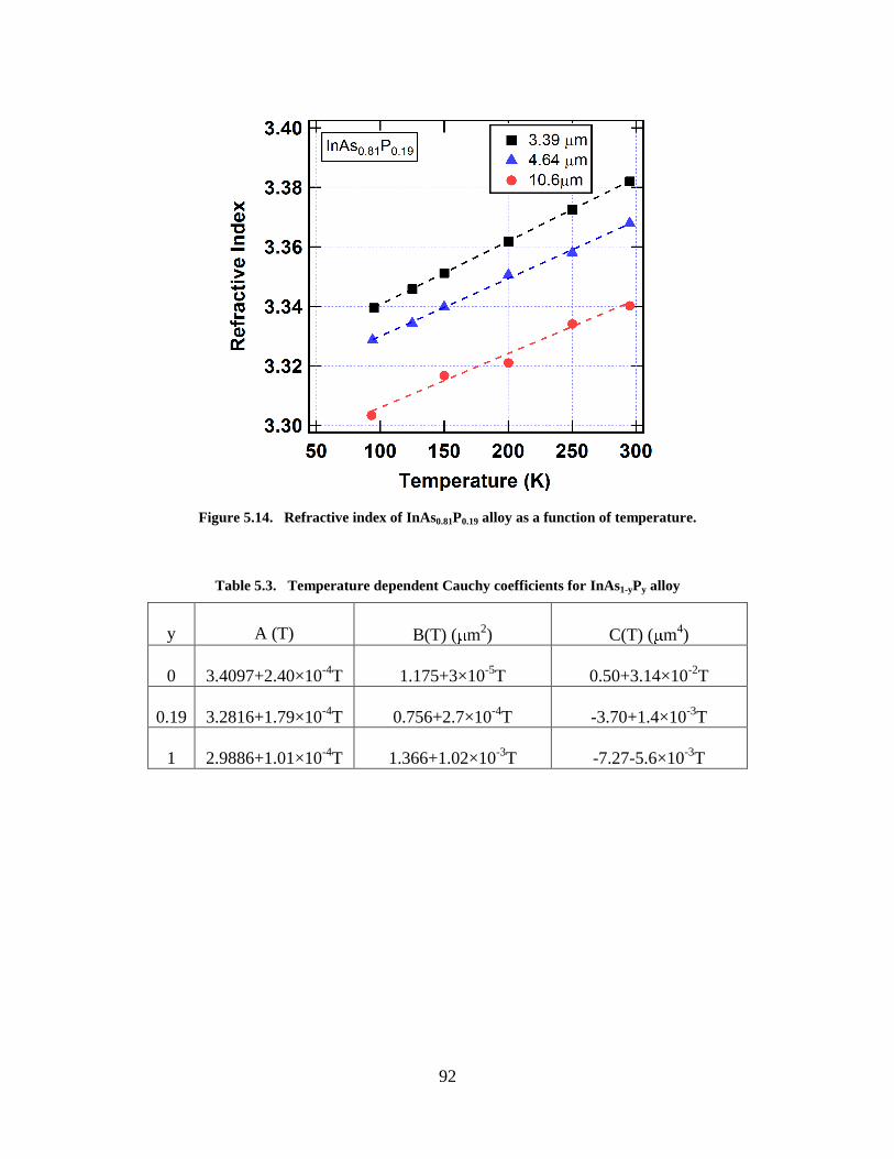
92
Figure 5.14. Refractive index of InAs0.81P0.19 alloy as a function of temperature.
Table 5.3. Temperature dependent Cauchy coefficients for InAs1-yPy alloy
y
A (T)
B(T) ( m2)
C(T) ( m4)
0
3.4097+2.40×10⁻⁴
T
1.175+3×10⁻⁵
T
0.50+3.14×10⁻²
T
0.19
3.2816+1.79×10⁻⁴
T
0.756+2.7×10⁻⁴
T
-3.70+1.4×10⁻³
T
1
2.9886+1.01×10⁻⁴
T
1.366+1.02×10⁻³
T
-7.27-5.6×10⁻³
T

93
Figure 5.15. Refractive index of InAs0.81P0.19 alloy as a function of wavelength.
Refractive indices of InAs1-yPy alloys versus full composition at a wavelength of 4.6 m
and at two temperatures (95 and 295K) are shown in Fig. 5.16. Refractive indices at
other wavelengths (3.39 and 10.6 m) were also obtained but are not shown here.
Refractive indices at 3.39 m are slightly greater than those measured at 4.6 m, and the
results at 4.6 m are greater than those measured at 10.6 m. However, the difference
from different wavelengths is not significant compared to the variations in indices from
different compositions.

94
Figure 5.16. Refractive Index of InAs0.81P0.19 measured at 4.6 m, and at 95 K and 295 K as a
function of composition.
Earlier work in ternary material properties was based on using linear proportionality with
respect to binary semiconductors [42, 43], and adding the bowing factor by using
quadratic terms. But this method does not apply to the composition-dependent refractive
index of InAs0.81P0.19 alloy. From Fig. 5.16, the best fit function is an exponential
function, which can be expressed as
yen 340.25313.00255.3 at 295 K and at 4.6 m (5.3)
yen 116.25065.09883.2 at 95 K and at 4.6 m (5.4)
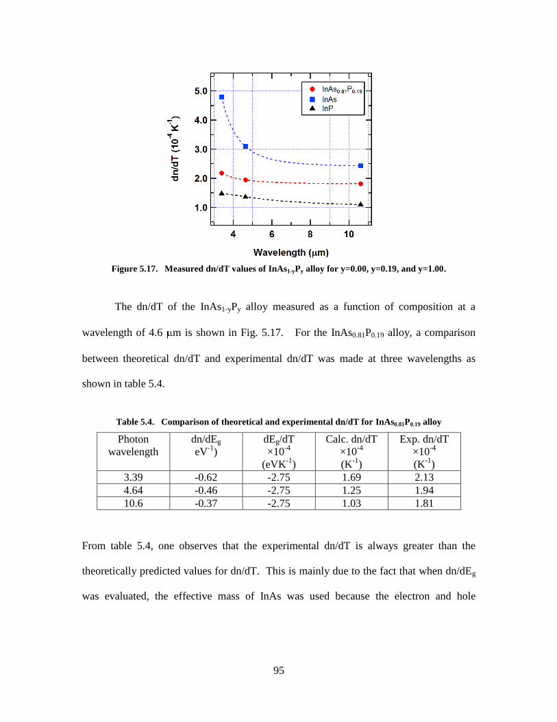
95
Figure 5.17. Measured dn/dT values of InAs1-yPy alloy for y=0.00, y=0.19, and y=1.00.
The dn/dT of the InAs1-yPy alloy measured as a function of composition at a
wavelength of 4.6 m is shown in Fig. 5.17. For the InAs0.81P0.19 alloy, a comparison
between theoretical dn/dT and experimental dn/dT was made at three wavelengths as
shown in table 5.4.
Table 5.4. Comparison of theoretical and experimental dn/dT for InAs0.81P0.19 alloy
Photon
wavelength
dn/dEg
eV-1
)
dEg/dT
×10-4
(eVK-1
)
Calc. dn/dT
×10-4
(K-1
)
Exp. dn/dT
×10-4
(K-1
)
3.39 -0.62 -2.75 1.69 2.13
4.64 -0.46 -2.75 1.25 1.94
10.6 -0.37 -2.75 1.03 1.81
From table 5.4, one observes that the experimental dn/dT is always greater than the
theoretically predicted values for dn/dT. This is mainly due to the fact that when dn/dEg
was evaluated, the effective mass of InAs was used because the electron and hole
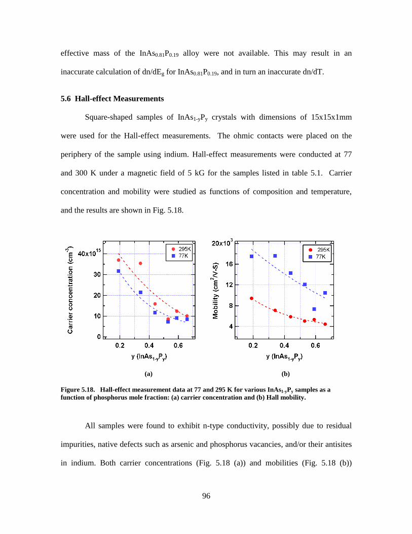
96
effective mass of the InAs0.81P0.19 alloy were not available. This may result in an
inaccurate calculation of dn/dEg for InAs0.81P0.19, and in turn an inaccurate dn/dT.
5.6 Hall-effect Measurements
Square-shaped samples of InAs1-yPy crystals with dimensions of 15x15x1mm
were used for the Hall-effect measurements. The ohmic contacts were placed on the
periphery of the sample using indium. Hall-effect measurements were conducted at 77
and 300 K under a magnetic field of 5 kG for the samples listed in table 5.1. Carrier
concentration and mobility were studied as functions of composition and temperature,
and the results are shown in Fig. 5.18.
(a) (b)
Figure 5.18. Hall-effect measurement data at 77 and 295 K for various InAs1-yPy samples as a
function of phosphorus mole fraction: (a) carrier concentration and (b) Hall mobility.
All samples were found to exhibit n-type conductivity, possibly due to residual
impurities, native defects such as arsenic and phosphorus vacancies, and/or their antisites
in indium. Both carrier concentrations (Fig. 5.18 (a)) and mobilities (Fig. 5.18 (b))
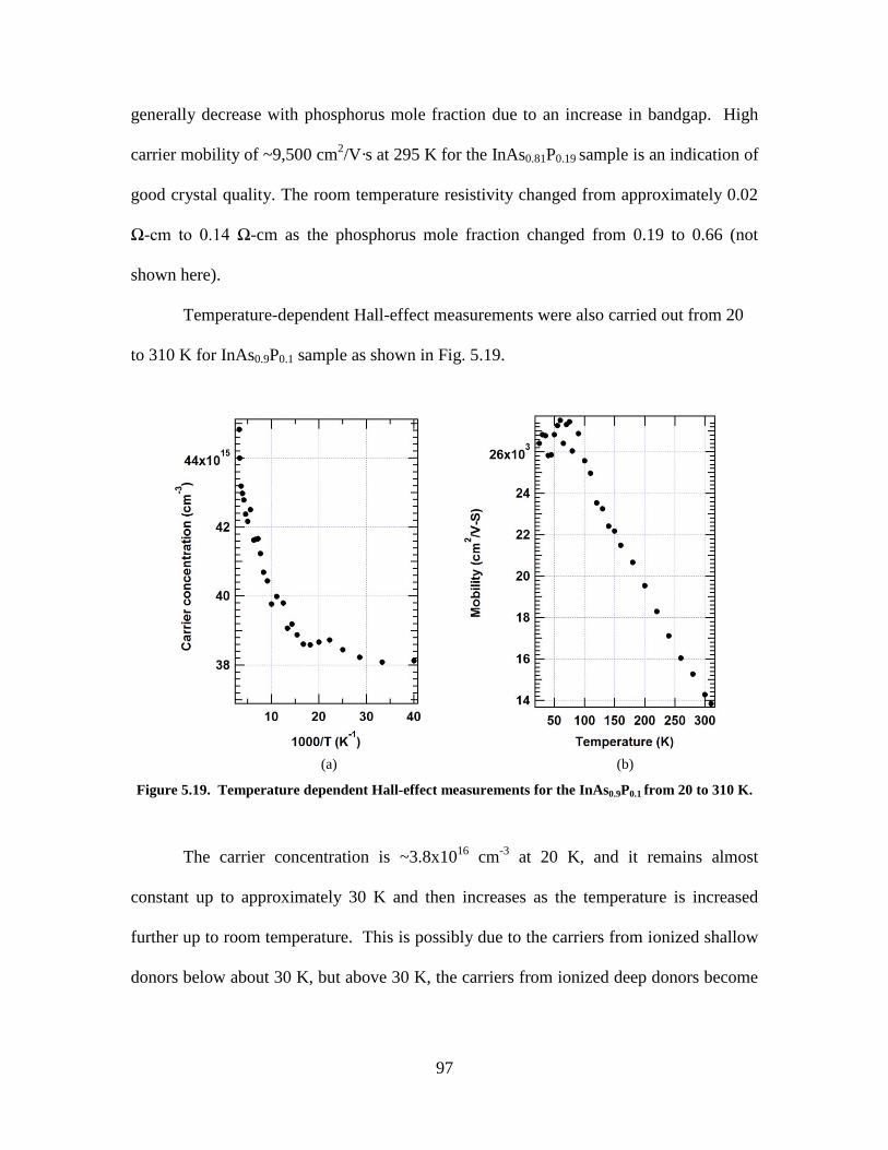
97
generally decrease with phosphorus mole fraction due to an increase in bandgap. High
carrier mobility of ~9,500 cm2/V·s at 295 K for the InAs0.81P0.19 sample is an indication of
good crystal quality. The room temperature resistivity changed from approximately 0.02
Ω-cm to 0.14 Ω-cm as the phosphorus mole fraction changed from 0.19 to 0.66 (not
shown here).
Temperature-dependent Hall-effect measurements were also carried out from 20
to 310 K for InAs0.9P0.1 sample as shown in Fig. 5.19.
(a) (b)
Figure 5.19. Temperature dependent Hall-effect measurements for the InAs0.9P0.1 from 20 to 310 K.
The carrier concentration is ~3.8x10¹⁶
cm-3
at 20 K, and it remains almost
constant up to approximately 30 K and then increases as the temperature is increased
further up to room temperature. This is possibly due to the carriers from ionized shallow
donors below about 30 K, but above 30 K, the carriers from ionized deep donors become

98
dominant in the conduction band. The mobility remains about the same at temperatures
up to 50 K and then increases due to screening of ionized impurity scattering and/or alloy
disorder scattering. The mobility is 2.8 104 cm
2/V·s at 75 K, and then decreases as the
sample temperature is increased to 310 K due to increase in optical phonon lattice
scattering at higher temperatures.
99
6. Results and Discussions on Bulk Ternary InxGa1-xAs
Undoped bulk melt-grown InxGa1-xAs was fabricated using the vertical Bridgman
technique by United Semiconductor LLC. The electrical and optical properties of InxGa1-
xAs were investigated as functions of indium mole fraction and sample temperature in a
similar manner to those of InAs1-yPy in chapter 5, some of the results are accepted for
publish [86]. The optical properties of interest include bandgap energies and refractive
index, and the electrical properties include carrier concentration, mobility, and resistivity.
A systematic measurement of PL was carried out in order to gain insight into the
various radiative transitions in the InxGa1-xAs crystal. The discussions include PL
measurements as functions of temperature, laser excitation power, and sample location.
6.1 Ternary InxGa1-xAs Crystal Growth
Undoped bulk InxGa1-xAs (0 x 1) polycrystals were grown using a multi-zone
vertical gradient freezing furnace at United Semiconductor LLC by Geeta Rajapopalan.
Here a description of her growth technique is provided for reference.
Melt synthesis was carried out using 6N purity polycrystalline GaAs and InAs as the
starting material. Appropriate mole fractions of InAs and GaAs were used according to the
liquidus composition which corresponded to a desirable crystal composition. The synthesis
and growth was conducted in a sealed silica crucible with a vacuum level of 10-7 Torr. During
the InGaAs synthesis, the molten InAs and GaAs mixtures were vigorously mixed by
periodically tilting the crucible along with the furnace. Typical synthesis duration was in the
range of 1-2 hours. Following synthesis, the melt was directionally cooled to grow the
crystal at a rate of 1 mm/hr. The temperature gradient near the melt-solid interface during
100
the growth was maintained in the range of 5-10 oC/cm. After the entire melt had solidified,
the crystal was cooled at a rate of 50 oC/hr to room temperature. During this process, the
melt composition continuously changed for grading the alloy composition of the crystal. In
order to grow a homogeneous crystal of a specific composition, the melt needs to be
maintained at a constant composition throughout the growth. In these processes, precise
control over the solute feeding process and melt composition is necessary [41].
In addition, there are other important parameters that must also be used to obtain
crystals with high optical and electrical properties. These growth parameters include: usage
of melt encapsulation, vapor pressure control for group V volatile species, crucible material
and post growth crystal annealing. Post growth cooling cycles for ternary crystals also needs
to be optimized. Faster cooling rates could lead to the thermal strain, inducing cracks in the
wafers during processing.
After growth, the InxGa1-xAs crystal’s boule was obtained (shown in Fig. 6.1 (a)) and
then sliced into wafers (shown in Fig. 6.1 (b)) using a diamond blade saw. The surfaces of
the wafers were ground using 14 µm boron carbide or silicon carbide abrasives followed by
chemo-mechanical polishing using 1µm and 0.5 µm alumina abrasive slurries. After the final
polishing step, high quality optical surfaces were obtained.
The optical quality is qualitatively checked using a Santa Barbara Focalplane
ImagIR MIR infrared camera. A typical MIR image of InxGa1-xAs is shown in
Fig. 6.1 (c). Each InxGa1-xAs wafer has dimensions of a ~50 mm diameter and a ~2 mm
thickness. Samples selected for Hall-effect measurements were sent back to USL to thin
and cut down to dimensions of 10x10x0.5 mm. Unlike InAs1-yPy, all refractive index
measurements of InxGay1-xAs crystals were carried out using Michelson and Fabry-Perot
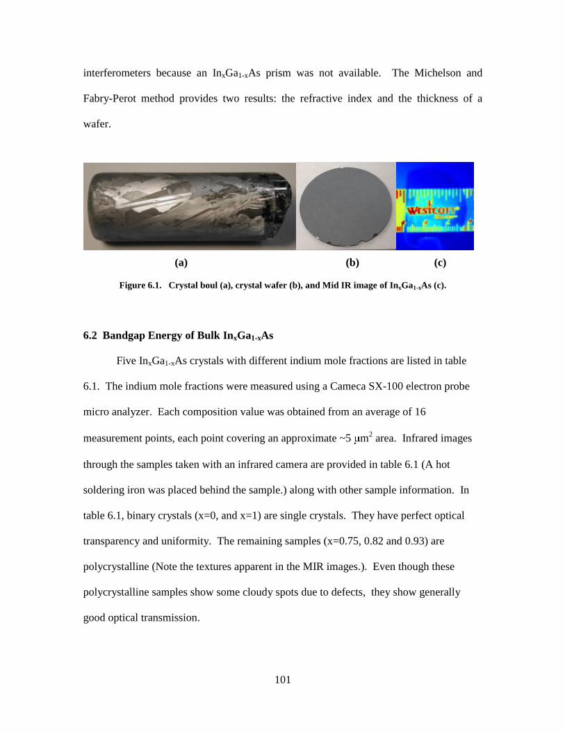
101
interferometers because an InxGa1-xAs prism was not available. The Michelson and
Fabry-Perot method provides two results: the refractive index and the thickness of a
wafer.
(a) (b) (c)
Figure 6.1. Crystal boul (a), crystal wafer (b), and Mid IR image of InxGa1-xAs (c).
6.2 Bandgap Energy of Bulk InxGa1-xAs
Five InxGa1-xAs crystals with different indium mole fractions are listed in table
6.1. The indium mole fractions were measured using a Cameca SX-100 electron probe
micro analyzer. Each composition value was obtained from an average of 16
measurement points, each point covering an approximate ~5 m2 area. Infrared images
through the samples taken with an infrared camera are provided in table 6.1 (A hot
soldering iron was placed behind the sample.) along with other sample information. In
table 6.1, binary crystals (x=0, and x=1) are single crystals. They have perfect optical
transparency and uniformity. The remaining samples (x=0.75, 0.82 and 0.93) are
polycrystalline (Note the textures apparent in the MIR images.). Even though these
polycrystalline samples show some cloudy spots due to defects, they show generally
good optical transmission.

102
Table 6.1. Various InxGa1-xAs crystals
Name GaAs 127-
24-4
IGA 041506-1 IGA 052406-1 IGA 052406-4 InAs WT
524-10
y 0.000 0.751 ± 0.004 0.821± 0.005 0.926 ± 0.002 1.000
Thickness
at 295 K
0.617 1.653 1.004 1.300 1.004
Thickness
at 100 K
0.616 1.648 1.001 1.296 1.001
MIR
images
Room temperature transmission spectra of these InxGay1-xAs samples are
measured using the Perkin Elmer Spectrum GX (FTIR spectrometer), and the results are
shown in Fig. 6.2 (top). Derivatives of transmission spectra with respect to photon
energy were plotted as a function of photon energy as shown in Fig.6.2 (bottom). EL min
values were determined from the peak locations of Fig. 6.2. EL min is known to be equal
to Eg if the sample thickness reaches zero (see chapter 4). For a sample having a
thickness > 1 mm, the difference of (Eg - EL min) is approximately a constant. For InAs,
this constant is approximately ~30 meV at room temperature, and ~45 meV for GaAs.
For InxGa1-xAs, this constant should be contributed from both InAs and GaAs, and could
be proportional to its composition. This leads to a correction factor that is equal to
(x*0.030 + (1-x)*0.045) eV, and this value can be added to EL min to obtain an
approximate value of the bandgap energy. The results were plotted in Fig. 6.3, along
with the thin film bandgap energies calculated using equation 6.1 [81]:
Eg (x) = 0.356 + 0.7(1-x) + 0.4(1-x)2. (6.1)
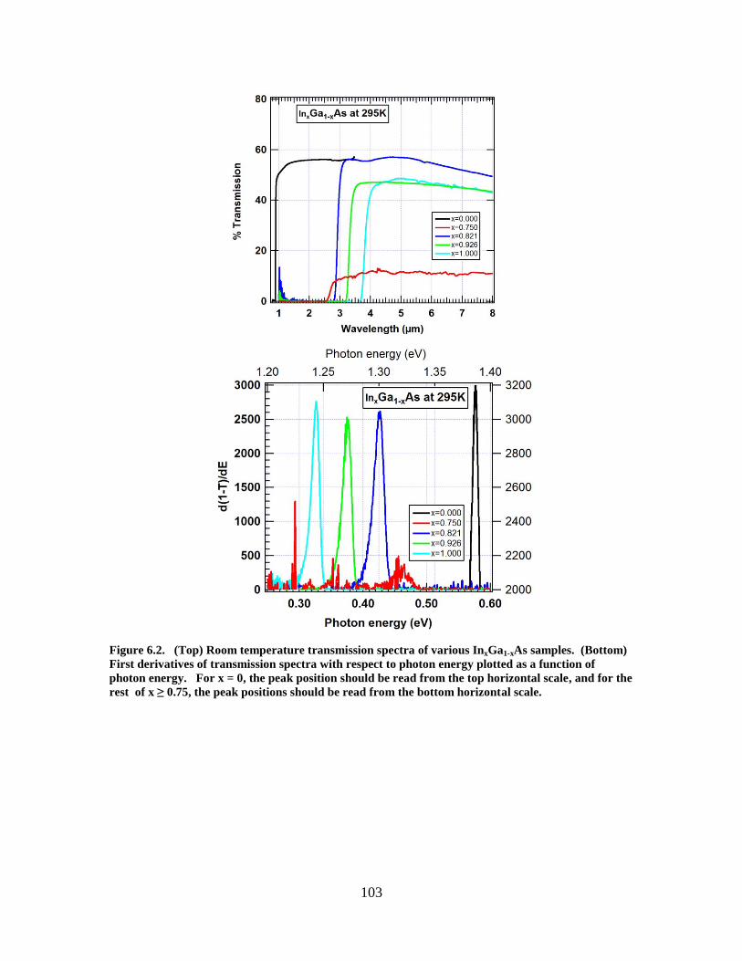
103
Figure 6.2. (Top) Room temperature transmission spectra of various InxGa1-xAs samples. (Bottom)
First derivatives of transmission spectra with respect to photon energy plotted as a function of
photon energy. For x = 0, the peak position should be read from the top horizontal scale, and for the
rest of x ≥ 0.75, the peak positions should be read from the bottom horizontal scale.
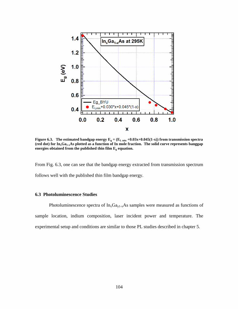
104
Figure 6.3. The estimated bandgap energy Eg = (EL min +0.03x+0.045(1-x)) from transmission spectra
(red dot) for InxGa1-xAs plotted as a function of In mole fraction. The solid curve represents banggap
energies obtained from the published thin film Eg equation.
From Fig. 6.3, one can see that the bandgap energy extracted from transmission spectrum
follows well with the published thin film bandgap energy.
6.3 Photoluminescence Studies
Photoluminescence spectra of InxGay1-xAs samples were measured as functions of
sample location, indium composition, laser incident power and temperature. The
experimental setup and conditions are similar to those PL studies described in chapter 5.
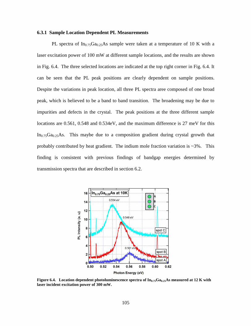
105
6.3.1 Sample Location Dependent PL Measurements
PL spectra of In0.75Ga0.25As sample were taken at a temperature of 10 K with a
laser excitation power of 100 mW at different sample locations, and the results are shown
in Fig. 6.4. The three selected locations are indicated at the top right corner in Fig. 6.4. It
can be seen that the PL peak positions are clearly dependent on sample positions.
Despite the variations in peak location, all three PL spectra aree composed of one broad
peak, which is believed to be a band to band transition. The broadening may be due to
impurities and defects in the crystal. The peak positions at the three different sample
locations are 0.561, 0.548 and 0.534eV, and the maximum difference is 27 meV for this
In0.75Ga0.25As. This maybe due to a composition gradient during crystal growth that
probably contributed by heat gradient. The indium mole fraction variation is ~3%. This
finding is consistent with previous findings of bandgap energies determined by
transmission spectra that are described in section 6.2.
Figure 6.4. Location dependent photoluminescence spectra of In0.75Ga0.25As measured at 12 K with
laser incident excitation power of 300 mW.

106
Sample position dependent PL spectra of In0.82Ga0.18As sample were also
measured and the results are plotted in Fig. 6.5. The PL measurements were conducted at
12 K with a laser power of 100 mW. The PL spectra shown in Fig. 6.5 are composed of
two strong peaks indicated by A and B, which correspond to the free exciton and the
donor to acceptor pair transitions, respectively. A very weak third PL peak is also visible
in the low energy region of the PL spectrum.
As seen from Fig. 6.5, the PL peak positions are clearly sample position dependent. The
maximum difference in the FX peak energy is about 7 meV, which indicates about 1%
indium composition variation. This variation is much smaller than those found in sample
In0.75Ga0.25As sample, demonstrating that In0.82Ga0.18As sample has better uniformity than
the In0.75Ga0.25As sample. Other observations are also support this conclusion. Firstly,
the FX peak is observed for In0.82Ga0.18As sample as shown in Fig. 6.5. On the other
hand, a broad B-B peak is observed for In0.75Ga0.25As sample as shown in Fig. 6.4. In
general, the FX peak can only be seen in pure crystals (see chapter 2). Secondly, the
In0.82Ga0.18As sample has higher optical transmission (~4.5 times) than In0.75Ga0.25 sample
as shown in Fig. 6.2 (a). Finally, IR images listed in table 6.1 show that the In0.75Ga0.25As
sample has more localized defect spots than the In0.82Ga0.18As sample.

107
D
BC
A
E
Figure 6.5. Position-dependent photoluminescence spectra for the In0.82Ga0.18As measured at 12 K at
five different positions with a laser excitation power of 400 mW.

108
6.3.2 Laser Excitation Power Dependent PL Measurements
As described in the previous section, power-dependent PL results can be used to
identify the transition origin because the relationship between the integrated PL peak
intensity and the laser excitation power is dependent on the nature of the PL transition. A
linear relationship between the excitation power and the integrated PL intensity indicates
an excitonic recombination; a sub-linear relationship indicates a defect or impurity
related transition; and a quadratic dependence indicates a band-to-band transition
[82, 83]. Laser excitation power dependent PL spectra were measured for both
In0.75Ga0.25As and In0.82Ga0.18As crystals at 12 K, and the results are discussed in this
section.
The laser excitation power dependent PL spectra for sample In0.75Ga0.25As
measured at 12 K are shown in Fig. 6.6. There is a broad peak marked as A at 0.572 eV,
and there is another weak peak near 0.55 eV when the laser power is below 200 mW.
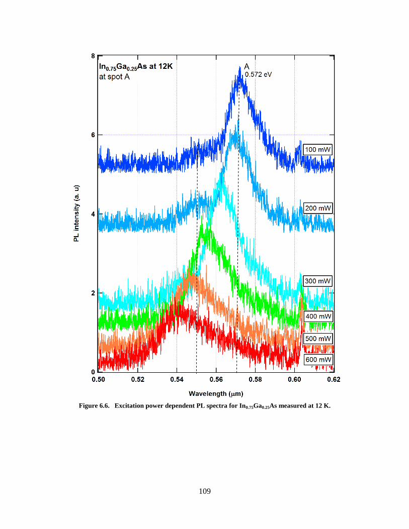
109
Figure 6.6. Excitation power dependent PL spectra for In0.75Ga0.25As measured at 12 K.
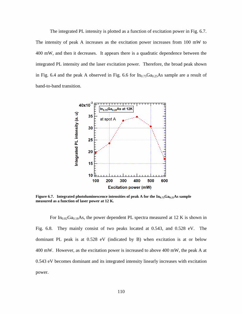
110
The integrated PL intensity is plotted as a function of excitation power in Fig. 6.7.
The intensity of peak A increases as the excitation power increases from 100 mW to
400 mW, and then it decreases. It appears there is a quadratic dependence between the
integrated PL intensity and the laser excitation power. Therefore, the broad peak shown
in Fig. 6.4 and the peak A observed in Fig. 6.6 for In0.75Ga0.25As sample are a result of
band-to-band transition.
Figure 6.7. Integrated photoluminescence intensities of peak A for the In0.75Ga0.25As sample
measured as a function of laser power at 12 K.
For In0.82Ga0.18As, the power dependent PL spectra measured at 12 K is shown in
Fig. 6.8. They mainly consist of two peaks located at 0.543, and 0.528 eV. The
dominant PL peak is at 0.528 eV (indicated by B) when excitation is at or below
400 mW. However, as the excitation power is increased to above 400 mW, the peak A at
0.543 eV becomes dominant and its integrated intensity linearly increases with excitation
power.
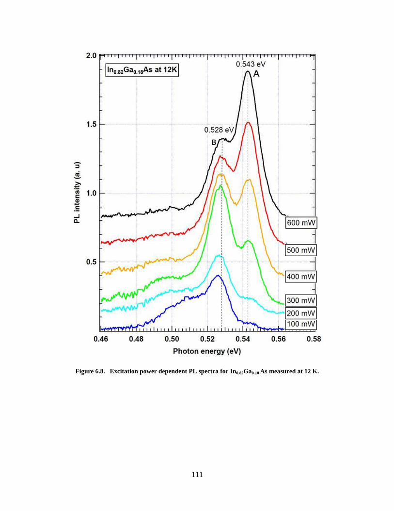
111
Figure 6.8. Excitation power dependent PL spectra for In0.82Ga0.18 As measured at 12 K.

112
The integrated PL intensities of In0.82Ga0.18As aree plotted in Fig. 6.9. Since the
integrated PL intensity of peak A clearly shows a linear dependence on excitation power,
the luminescence peak A is attributed to an excitonic recombination. On the other hand,
the integrated PL intensity of peak B initially increases up to an excitation power of
300 mW, and then decreases gradually with increasing excitation power. This sub-linear
relationship indicates that the peak B can be attributed to a DAP transition, which is also
consistent with the finding that peak B blue-shift as the excitation power increases as
shown in Fig. 6.8.
Figure 6.9. Integrated photoluminescence intensities of peaks A and B for the In0.82Ga0.19As sample
measured as a function of laser power at 12 K.

113
6.3.3 Temperature Dependent PL Measurements
PL spectra of the In0.75Ga0.25As sample wre measured at a temperature range of
10 – 130 K, and the results are shown in Fig. 6.10. These spectra were taken at spot B on
the sample location as indicated at the top right in Fig. 6.4. All spectra show a broad
band-to-band recombination peak, and these peaks are broadened and weakened as
temperature increases. In addition, the PL peaks red-shift as temperature increases,
which is due to Eg decreasing as the temperature increases. The band to band transition
peak red shifts by approximately 30 meV as the temperature changes from 12 to 130 K.
The PL spectra for sample In0.82Ga0.18As were also measured at various
temperatures and are shown in Fig. 6.11. The PL peak positions indicated by A (FX
transition) are red-shifted by approximately 30 meV as the temperature is increased from
12 to 190 K. The peak A persists up to 200 K with decreasing intensity. However, the
intensity of the peak B decreases much more rapidly with increasing temperature and
completely disappears above 50 K. As shown in Fig. 6.11, both peaks show a red-shift
with increasing temperature due to bandgap shrinkage.

114
0.548 eV
0.519 eV
Figure 6.10. Temperature dependent PL spectra for In0.75Ga0.25As with a laser power of 300 mW.

115
Figure 6.11. Temperature dependent PL spectra for the In0.82Ga0.18As sample measured with a laser
excitation power of 300 mW.
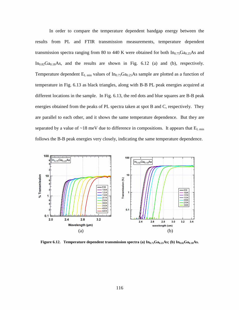
116
In order to compare the temperature dependent bandgap energy between the
results from PL and FTIR transmission measurements, temperature dependent
transmission spectra ranging from 80 to 440 K were obtained for both In0.75Ga0.25As and
In0.82Ga0.18As, and the results are shown in Fig. 6.12 (a) and (b), respectively.
Temperature dependent EL min values of In0.75Ga0.25As sample are plotted as a function of
temperature in Fig. 6.13 as black triangles, along with B-B PL peak energies acquired at
different locations in the sample. In Fig. 6.13, the red dots and blue squares are B-B peak
energies obtained from the peaks of PL spectra taken at spot B and C, respectively. They
are parallel to each other, and it shows the same temperature dependence. But they are
separated by a value of ~18 meV due to difference in compositions. It appears that EL min
follows the B-B peak energies very closely, indicating the same temperature dependence.
(a) (b)
Figure 6.12. Temperature dependent transmission spectra (a) In0.75Ga0.25As; (b) In0.82Ga0.18As.

117
Figure 6.13. Temperature dependent B-B transition energies of In0.75Ga0.25As sample taken at two
sample locations. (Red dot taken at spot B, blue square taken at spot C), along with EL min (black
triangle) obtained from transmission spectra.
(a) (b)
Figure 6.14. (a) Temperature dependent FX peaks (red dots) and EL min (blue square) of the
In0.82Ga0.18As; (b) Eg (black triangle) calculated using TEE Lg min with = 0.0035 eVK
-0.5
plotted as a function of temperature. The solid curve is Varshni equation fit.
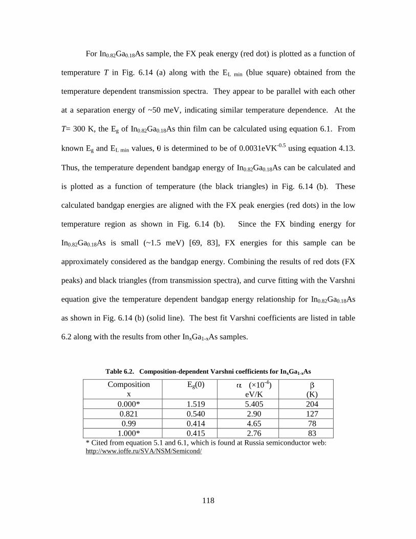
118
For In0.82Ga0.18As sample, the FX peak energy (red dot) is plotted as a function of
temperature T in Fig. 6.14 (a) along with the EL min (blue square) obtained from the
temperature dependent transmission spectra. They appear to be parallel with each other
at a separation energy of ~50 meV, indicating similar temperature dependence. At the
T= 300 K, the Eg of In0.82Ga0.18As thin film can be calculated using equation 6.1. From
known Eg and EL min values, is determined to be of 0.0031eVK-0.5
using equation 4.13.
Thus, the temperature dependent bandgap energy of In0.82Ga0.18As can be calculated and
is plotted as a function of temperature (the black triangles) in Fig. 6.14 (b). These
calculated bandgap energies are aligned with the FX peak energies (red dots) in the low
temperature region as shown in Fig. 6.14 (b). Since the FX binding energy for
In0.82Ga0.18As is small (~1.5 meV) [69, 83], FX energies for this sample can be
approximately considered as the bandgap energy. Combining the results of red dots (FX
peaks) and black triangles (from transmission spectra), and curve fitting with the Varshni
equation give the temperature dependent bandgap energy relationship for In0.82Ga0.18As
as shown in Fig. 6.14 (b) (solid line). The best fit Varshni coefficients are listed in table
6.2 along with the results from other InxGa1-xAs samples.
Table 6.2. Composition-dependent Varshni coefficients for InxGa1-xAs
Composition
x
Eg(0) (×10-4
)
eV/K (K)
0.000* 1.519 5.405 204
0.821 0.540 2.90 127
0.99 0.414 4.65 78
1.000* 0.415 2.76 83 * Cited from equation 5.1 and 6.1, which is found at Russia semiconductor web:
http://www.ioffe.ru/SVA/NSM/Semicond/

119
6.4 Refractive Index Measurements
Refractive index measurements on wafer shaped InxGa1-xAs crystals were
performed as functions of wavelength, temperature, and indium composition using
Michelson and Fabry-Perot interferometers. The detailed refractive-index measurement
method and experimental setup were described in section 3.4.
After the calibration procedure, refractive indices of InxGa1-xAs crystals were
measured using 4.6 m and 10.6 m laser beams at temperatures 100 and 295 K. The
results are plotted as a function of indium composition in Fig. 6.15 (a) for 4.6 m and (b)
for 10.6 m. For the full composition range (0≤ x ≤1), the refractive indices follow a
quadratic relation to the composition. The quadratic fitting expressions are listed in
table 6.3.
(a) (b)
Figure 6.15. Refractive indices of bulk InxGa1-xAs measured at 100 and 295 K using Michelson and
Fabry-Perot method (a) measured at 4.6 m and (b) measured at 10.6 m.

120
Table 6.3. Refractive index of InxGa1-xAs as a function of composition at various wavelengths and
temperatures
Sample Conditions Refractive Index, n(x, , T)
At 4.6 m and at 100 K 3.259+0.175x+0.070x2
At 4.6 m and at 295 K 3.296+0.180x+0.070x2
At 10.6 m and at 100 K 3.225+0.031x+0.200x2
At 10.6 m and at 295 K 3.258+0.037x+0.200x2
Note: Michelson and Fabry-Perot interferometry methods are very sensitive to defects in
the crystal, and it was a challenge to accurately measure the refractive index for
polycrystalline InxGa1-xAs using these methods. For this work, the accuracy of refractive
index is only ±0.01, which is far less than the achievable accuracy using the minimum
deviation method. The uncertainty is included as an error bar in Fig. 6.15.
6.5 Hall-effect Measurements
Square shaped wafer of InxGa1-xAs crystal with dimensions 10x10x0.5 mm3 was
used for the Hall-effect measurements. The ohmic contacts were placed on the periphery
of the sample using indium. Hall-effect measurements were conducted at 77 and 300 K
with a magnetic field of 5 kG for samples with different indium mole fractions. Carrier
concentration and Hall mobility were studied as functions of composition and
temperature, and the results are shown in Fig. 6.16 (a) for carrier concentration and (b)
for Hall mobility.

121
(a) (b)
Figure 6.16. Hall-effect measurement results at 77 and 300 K for various InxGa1-xAs samples as a
function of indium mole fraction: (a) carrier concentration and (b) Hall mobility.
All samples were found to exhibit n-type conductivity, which was possibly due to
residual impurities and native defects, such as indium and gallium vacancies and/or their
antisites. Both carrier concentration and mobility generally increase with indium content
due to a decrease in bandgap energy. High carrier mobility of 16,000 cm2V
-1S
-1 at 295 K
for In0.91Ga0.09As sample is an indication of a good crystal. Resistivity at room
temperature changes from approximately 0.4 to 0.02 Ω-cm as the indium mole fraction
increases from 0.5 to 1 (not shown here).
122
7. Conclusions and Future Work
Optical and electrical properties of bulk, melt-grown InAs1-yPy and InxGa1-xAs
polycrystals were investigated as functions of phosphorus and indium compositions and
temperatures using the photoluminescence (PL), Fourier transform infrared (FTIR)
transmission spectroscopy, refractive index, and Hall-effect measurements.
These ternary alloys with diameters up to 50 mm were grown using the vertical
Bridgman technique. The critical growth conditions for large diameter (50 mm) crack
free bulk ternary InAs1-yPy and InxGa1-xAs polycrystals were briefly described in this
dissertation. The as-grown undoped bulk ternary InAs1-yPy and InxGa1-xAs polycrystals
have been found to exhibit n-type conductivity irrespective of the alloy compositions.
This is possibly due to residual impurities and native defects, such as indium and gallium
vacancies, and/or their antisites for InxGa1-xAs samples, and arsenic and phosphorus
vacancies, and/or their antisites for InAs1-yPy sample. Although the bulk InAs1-yPy and
InxGa1-xAs crystals showed good optical transmission in the infrared and high carrier
mobility, they exhibited random compositional fluctuations across the substrate area.
The refractive index, transport properties, and below-bandgap transmission were
presented here as a function of alloy composition and temperature for the first time, to the
best of our knowledge. A practical method of extracting bandgap energies directly from
the FTIR transmission spectra has been presented in this work. The method was verified
to several binary semiconductors with known bandgaps and was applied to determine the
unknown properties of novel ternary semiconductors InxGa1-xAs and InAs1-yPy. The
results are promising, although further improvement is required. Bandgap energies
123
estimated from the transmission spectra agree well with those obtained from PL peaks
and the previously reported values from the thin film studies.
FTIR spectra were measured for all these ternary samples, and they showed little
or no absorption for photon energy less than bandgap. The temperature dependent
bandgap energies and temperature dependent refractive indices were also able to be
extracted from the composition and temperature dependent FTIR transmission spectra.
This process involves taking the derivative of the transmission with respect to photon
energy (dT/dE). A Gaussian-like curve was observed for all (dT/dE) studied when it is
plotted as a function of photon energy. The values of EL min could be determined from the
peak locations of (dT/dE). Then, using the relationship, TEE Lg min , the bandgap
energy (Eg) was obtained. The fitting parameter θ can be determined from the known
bandgap energy at a given temperature (for instance, the bandgap energy of the thin films
at room temperature). This method of bandgap estimation from the FTIR transmission
spectra shows very promising results for InAs, InP, GaAs, InAs1-yPy, and InxGa1-xAs.
A systematic measurement of photoluminescence was carried out in order to gain
insight into the various radiative transitions in InAs1-yPy and InxGa1-xAs crystals. This
study includes temperature, laser excitation power, and sample position dependent PL
measurements. The excitation power-dependent PL results can be used to identify the
origin of the transition because the relationship between the integrated PL peak intensity
and the laser excitation power is dependent on the nature of the PL transition. The results
of PL measurements show that free exciton (FX) transitions are dominant for high quality
InAs1-yPy and InxGa1-xAs crystals. The temperature dependent PL measurements show
that PL peaks red-shift with increasing temperature due to the bandgap decreasing as a

124
result of lattice expansion and phonon vibration. The FX peak positions of InAs0.81P0.19
are red-shifted by approximately 40 meV as temperature changes from 12 to 130 K. The
FX peak positions of In0.82Ga0.18As are red-shifted by approximately 30 meV as
temperature changes from 12 to 190 K. The red-shift is also observed with an increase of
indium mole fraction for InxGa1-xAs and a decrease of the phosphorus mole fraction for
the InAs1-yPy crystal. The FX peak positions of InxGa1-xAs are red-shifted from 0.568 to
0.412 eV as an indium mole fraction increases from 0.75 to 0.99.
Temperature-dependent bandgap energies were also obtained from temperature-
dependent PL spectra, and the results were compared with those obtained from the
transmission spectra as well as the published thin film data. It shows that both results are
in good agreement with each other and also they fit well with the Varshni expression.
Varshni coefficients over temperature range of 10 - 400 K were obtained for the first time
for the bulk InxGa1-xAs at x=0.82 and 0.99, and for the InAs1-yPy at y = 0.19, 0.24, and
0.34.
From the location dependent PL measurements, it has been observed a FX PL
peak energy variation on the order of 5 - 11 meV within a InxGa1-xAs wafer, indicating
about 1-3% of variation in composition across this bulk sample. Also the FX PL peak
locations of InA0.81P0.19 measured at 12 K are at 0.556, 0.575, and 0.594eV. This shows a
variation of 38 meV, indicating the variation in composition of about 5% across the
sample.
The refractive index of InAs0.81P0.19 was measured as functions of wavelength and
temperature using the minimum deviation method. At all three wavelengths (3.39, 4.64
and 10.60 m), the refractive index varied linearly in the temperature range between 90

125
and 295 K. Refractive indices of InAs1-yPy were also obtained for various compositions
at two temperatures with IR wavelength of 4.6, 3.39 and 10.6 m. The refractive indices
measured at 3.39 m are greater than those at 4.6 m, and those at 4.6 m are greater
than those measured at 10.6 m. However, the difference due to different photon
wavelengths is not significant compared to the variations in indices due to different
compositions. For InAs0.81P0.19, a comparison between theoretical dn/dT and
experimental dn/dT was made at three wavelengths, and they agreed reasonably well. In
order to improve the accuracy, an accurate electron effective mass of InAs0.81P0.19 is
needed in Kane energy (Ep) calculation.
The refractive index was measured for wafer shaped InxGa1-xAs crystals as
functions of wavelength, temperature and indium composition using Michelson and
Fabry-Perot interferometers. The refractive indices of full composition range (from 0 to1)
were obtained for the first time, to the best of our knowledge, for InxGa1-xAs at 4.6 and
10.6 m and at 100 and 295 K. Also, for the first time, the temperature dependent
refractive indices for InAs0.81P0.19 were obtained at wavelengths 3.39, 4.64 and 10.60 m,
and at temperatures ranging from 90 to 295 K.
All as-grown InxGa1-xAs samples show high mobilities, e.g., 4.8x10³ and
1.4x104 cm
2/V·s at 300 K for In0.75Ga0.25As and In0.99Ga0.01As, respectively, indicating a
good crystal quality. Both carrier concentration and mobility generally increase with
indium content due to a decrease in bandgap energy. All InxGa1-xAs and InAs1-yPy
samples show n-type conductivity. Carrier concentration for In0.5Ga0.5As at room
temperature is ~5x10¹⁵
cm-3
, and it increases with indium mole fraction.

126
For InAs1-yPy samples, both carrier concentration and mobility generally decrease
with phosphorus mole fraction due to an increase in bandgap. High carrier mobility of
8,200cm2/V·s at 295 K for the InAs0.81P0.19 sample is an indication of good crystal quality.
The room temperature resistivity changes from approximately 0.02 to 0.14 Ω-cm as the
phosphorus mole fraction increases from 0.19 to 0.66.
Temperature-dependent Hall-effect measurements were also carried out from 20
to 310 K for InAs0.9P0.1. The carrier concentration was 3.8x10¹⁶
cm-3
at 20 K, and
remained almost constant up to approximately 50 K, then it increases as the temperature
is increased further up to room temperature. The mobility remains about the same at
temperatures from 20 to 50 K, and then it starts to decrease linearly with temperature. It
reaches a peak mobility of 2.7 104 cm
2/V·s at 70 K, and then decreases to
1.4 104 cm
2/V·s as the sample temperature is increased to 300 K.
In summary, optical and electrical properties of bulk InxGa1-xAs and InAs1-yPy
crystals were systematically studied as functions of composition (indium mole fraction
for InxGa1-xAs and phosphorus mole fraction for InAs1-yPy in full range) and temperature
(ranging from 10 – 400 K). Many of these properties are reported for the first time, to the
best of our knowledge. It seems that it is more challenging to grow high quality ternary
crystals with small indium content (x) for InxGa1-xAs, and large phosphorus content (y)
for InAs1-yPy. Optical and electrical properties of these crystals are well suited for a
variety of applications that do not require a single crystal.
For future work, it would be very desirable to grow bulk InxGa1-xAs and InAs1-yPy
single crystals or perhaps polycrystals with a large enough area of single crystal section
so that the single crystal area can be used as a substrate for subsequent growth of good
127
epitaxial layers with a wide range of compositions. The presence of random macroscopic
composition fluctuations and the intrinsic defects formed in the crystals requires
refinement of crystal growth conditions. More efficient melt mixing processes or
enhancements with magnetic fields during crystal growth may help eliminate the intrinsic
defects formed in the crystals using current techniques. Undoubtedly, further
characterization studies are required for improved bulk ternary alloys. Also, work in the
temperature dynamics of carrier properties and on nonlinear optical properties of these
materials at various infrared wavelengths and temperatures will be needed to be carried
out. Newer materials and their applications need to be developed, and often binary and
ternary III-V compounds (GaSb, GaP, GaSbP etc) can also be studied using the method
developed in this work.

128
Appendix A
Related Publications
J. Wei, J. Barnes, S. Guha, L. P. Gonzalez, Y. K. Yeo, R. L. Hengehold and G.
Rajagopalan, “Electrical and Optical Characterization of Melt Grown Bulk InAs1-yPy
Crystals”, J. Electronics Materials, 40 (2) p1432-9 (2011).
Y. K. Yeo, A. C. Bergstrom, R. L. Hengehold, J. Wei, S. Guha and L. P. Gonzalez, G.
Rajagopalan, Mee-Yi Ryu, “Optical and Electrical Properties of Bulk-Grown Ternary
InxGa1-xAs”, Accepted for publication at Journal of the Korean Physical Society 2010.
Xiaofeng Duan, Jean Wei, Larry Burggraf, and David Weeks, “Mapping Ground-State
Properties of Silicon Carbide Molecular Clusters using Quantum Mechanical
Calculations: SimCn and SimCn-(m, n <4)”, Computational Material Science, 47 (3) p630-
644 (2010)
P. G. Schunemann, L. a. Pomeranz, K. T. Zawilski, Jean Wei, Leonel P. Gonzalez,
Shekhar Guha, T. M. Pollak, “Efficient Mid-infrared Optical Parametric Oscillator Based
on CdSiP2”, published in 2009 at Advances in Optical Materials, OSA.
J. W “Use of Quantum Mechanical Calculations to Investigate Small Silicon Carbide
Clusters” (Master thesis on file at Air Force Institute of Technology Academic Library,
2001)

129
Appendix B
Hall Effect Measurements
Sample and system preparation
Sample
1. Use the green card holder. Place the sample in the center of these pressure
pins.
2. Turn on the ultrasonic soldering iron.
3. Apply indium solder at the four corner of the squared sample as ohmic
contact.
4. Apply a small drop of rubber cement to the back of the sample using a
sharpened cotton swap stick. Place each one of the four pressure probes on
each contact.
5. Use the curve tracer (power on, memory 1, hit recall) to check the
connections, a vertical straight line indicates good ohmic contact.
6. Insert card into sample mount.
7. Connect the 4 yellow testing cables to the top of the sample probe.
8. Check that the temperature sensor cable is connected.
9. Turn on the water line to cool the magnets. Checks to make sure the return
water lines are open.
System Preparation
1. Check for water leaking from the connections at the back of the magnets.
2. Check the placement of the Gaussmeter.
3. Flip the switch on the front of the magnet power supply into stand by mode.
4. Make sure all the interlock lights are green. Hit the reset button if any are red.
5. Push the green button to power on the magnets.
6. Turn on equipment stack. (red button upper right side on cabinet)

130
7. Turn on the computer and log in with password Lake Shore.
8. Open the program from icon on desktop. (Hall Measurement System)
9. Make sure all equipment is functioning by checking the Systems Logs box in
the program.
Measurement
1. Choose a current to test the samples, one that works through the entire
temperature range.
Click on the resistivity button at the top right corner of the program.
Choose high or low resistivity.
Select the contact configuration to test (12, 12).
Select a current and click the measure button.
Monitor that the output is in range and that there are no errors.
Check that the current works for all contact pairs. (23,23; 34,34;
14,14)
2. Check that the contacts are linear.
Do an I-V test with the selected current chose a step that result in
about 5 measurement points. (right click in the measurements box on
the left and choose I-V measurement)
Choose high or low resistivity based on the sample material.
Choose default contact pairs, click ok.
Click the Start button at the top of the program.
3. Create a program for RT, HT or LT measurements. (right click in the
measurements box on the left and choose variable field of variable
temperature measurement)
Select Hall and resistivity measurements
Select to calculate resistivity at zero field.
Select a magnetic field of 5 kG; choose a step of 1 kG.

131
Enter the chosen current both positive and negative.
Select high or low resistivity.
Enter the temperatures for measurement.
* Temperature-dependent measurements take ~5 hours.
* Room temperature measurements with different three currents take ~20 min.
Shut Down
1. Turn off the magnets. (red button)
2. Put the magnet power supply out of stand by mode. (toggle switch)
3. Turn off water to magnets.
4. Turn off compressor after LT measurements.
5. Turn of water to the compressor.
6. Close the HMS.exe program.
7. Turn off computer monitor or entire stack if not going to use for awhile.
8. Wait for systems to return to room temperature. (294 K)
9. Turn off vacuum pump. (ONLY if system is at room temperature)
10. Wait for sample chamber to pressurize.
11. Unplug the necessary cables to remove sample mount.
12. Remove sample.
13. Assemble the sample chamber to keep dust and contaminants out while not in
use.

132
Photoluminescence Measurements
Sample and system preparation
1. Cleaning the sample surface with TCE, acetone, methanol, and DI water.
2. A Spectro-Physincs BeamLok 2085-20 Ar Ion laser is the exciting source.
This laser is chopped at ~170 Hz using a ThorLabs optical chopper.
3. Apply some crycon thermal grease on the back of sample and attach the
grease side to the cold finger that connected to the Helitran, the incident laser
and sample is approximately at 450 angle. Close the chamber and turn on the
vacuum pump.
4. Open the valve that connects the sample system and the liquid helium tank
after the vacuum reaches 20 mili-Torr, so the temperature can be cooled down
using evaporated liquid helium gas.
Measurement
1. After the temperature reaches approximately 10 K, adjust the collecting lenses
and sample angle so the photoluminescence enter the entrance slit of the
spectrometer (SPEX 750 M), the spectrometer is purged using high purity
nitrogen gas.
2. The intensity of photoluminescence spectra is measured using a Teledyne
Judson Technologies J10D InSb detector (it is liquid nitrogen-cooled and
operated with a 12 V bias preamplifier) and a lock-in amplifier which is
synchronized with the optical chopper.
3. Make sure to use a full range for the first scan; choose a lower resolution to
save time (only for the first scan). Then use a higher resolution after
identifying the main PL peak as well as adjusting the scan range according to
the PL peak location.
4. Conducting the sample location variation and laser power dependent as well
as temperature dependent PL spectra.
5. Adjust the temperature to the desired one using the Lakeshore temperature
controller by touching “sent the point” and press the up and down button then
press “enter”.
6. Adjust the laser power by adjusting output power using the laser control
panel.

133
Shut Down
1. Close the Helium gas flow meter (connect with the sample dewar).
2. Set the sample temperature to 295K.
3. Release the Helium tank valve (two yellow valve handles, release them
gently).
4. When sample chamber temperature reaches > 200K, unplug the heater
(connected to the Helium flow meter tube).
5. Shut down the laser. (turn the current to the minimum, turn the key to off).
6. Shut down the purge nitrogen gas. (Close N2 flow meter, close the main valve
of the N2 bottle).
7. Turn off the chiller.
8. Turn off the water connected to the chiller (yellow valve under the optical
table).
9. Turn off the optical chopper (controller power off).
10. Turn off the power supply connected to the preamplifier of the detector.
11. Close the spectrometer slot. (push down the nub)
12. By the time temperature reach 295K, choose heater off (on the Lake shore
temperature controller)
13. By the time the Helium release is complete, close one of the yellow valves,
and leave another yellow valve completely open (the one that has pressure
control)

134
Appendix C
Magnetic Field Reading Correction
Resistivity
Let BS = sample field and BP = field at magnetic pole.
S
real
HSB
RR
24,13
13,24 13,24 13,240depends on B-field
S S
real
B B BR R R
calculatedcomputer 24,1324,13
HSR
B
B
B
R
B
B
B
B
B
RR
S
P
P
real
S
P
P
P
S
real
HS
Let r = real and cc = computer calculated.
(1) cc
HS
S
Pr
HS RB
BR real accurate value to be obtained.
P
cc
HSB
RR
24,13← depends on applied B field
Hall Mobility
cc S
S
P
S
cc
HS
S
P
S
real
HSreal
HB
BR
B
BR
(2) cc S
S
Pr
HB
B

135
Carrier concentration
1 1 1
real ccS SS Sreal cc
ccHS P HS PPHS
S
B Bn n
eR B e R BBe R
B
(3) cc real SS S
P
Bn n
B
At two different fields: BP1, BP2, BS1, BS2
and 2
2,2,
1
1,1,
S
rr
HS
S
rr
HSB
RR
B
RR
1 2
,1 ,2
13,24 13,24 13,24 13,240 0and
S S S S
r r
B B B B B BR R R R R R
2
2
22,1
1
11, cc
HS
S
Pr
HS
cc
HS
S
Pr
HS RB
BRR
B
BR
2
2
22,1
1
11, cc
H
S
Pr
H
cc
H
S
Pr
HB
B
B
B
2
2
22,1
1
11, cc
S
P
Sr
S
cc
S
P
Sr
S nB
Bnn
B
Bn

136
We must have and 2,1,2,1, r
S
r
S
r
H
r
H nn
Then 1 2 1 21 21 2
1 2 1 2
or cc cc cc ccS SP PH H S S
S S P P
B BB Bn n
B B B B
If 2121
2
2
1
1 or then , cc
S
cc
S
cc
H
cc
H
S
P
S
P nnB
B
B
B
Also, S
r
HSr
H
S
r
HSr
H
RR 2,2,
1,1, and
Then 2
2
21
1
1 cc
HS
S
Pcc
HS
S
P RB
BR
B
B
If 1 2
1 21 2
1 2 1 2
, then that is r, r,
cc ccP PHS HS
S S P P
B B ΔR ΔRR R
B B B B
Therefore, 2,1, r
HS
r
HS RR

137
Bibliography
1. www.sarracenia.com/.../physics060.html
2. T. Baba, Y. Yogo, K. Suzuki, F. Koyama, and K. Iga, “Near room temperature
continuous wave lasing characteristics of GaInAsP/InP surface emitting laser”,
Electron. Lett. 29, p913-914, (1993).
3. T. Uchida, T. Uchida, F. Koyama, and K. Iga, “Control of GaInAs/InP layer thickness
for surface-emitting lasers by chemical beam epitaxy”, Electron. Communi. in Japan
Part II 75, p101-107, (1992).
4. S. H. Pyun and W. G. Jeong, “Luminescence characteristics of InGaAs/GaAs
quantum dots emitting near 1.5 m”, J. Korean Phys. Soc. 56, p586-590, (2010).
5. M. R. Soulby, D. G. Revin, J. P. Commin, A. B. Krysa, J. S. Roberts, and J. W.
Cockburn, “Probing diagonal laser transitions in InGaAs/InP quantum cascade
lasers”, J. Appl. Phys. 106, p123106-123109, (2009).
6. H. Shoji, T. Uchida, T. Kusunoki, M. Matsuda, H. Kurakake, S. Yamazaki, K.
Nakajima, and H. Ishikawa, “Fabrication of In0.25Ga0.75As/InGaAsP strained SQW
lasers on In0.05Ga0.95As ternary substrate”, IEEE Photon. Technol. Lett. 8, p1170-
1171, (1994).
7. A. H. Moore, B. Lent, and W. A. Bonner, “Fabrication of high power
InGaAs/AlInGaAs strained SQW lasers on InGaAs ternary substrates”, Electron. Lett.
32, p2018-2019, (1996).
8. H. Shoji, K. Otsubo, T. Kusunoki, T. Suzuki, T. Uchida, and H. Ishikawa,
“In0.38Ga0.62As/InAlGaAs/INGaP strained double quantum well lasers on
In0.21Ga0.79As ternary substrate”, Jpn. J. Appl. Phys. 35, L778-780, (1996).
9. A. M. Jones, B. Lent, J. F. Kluender, S. D. Roh, A. H. Moore, W. A. Bonner, and J. J.
Coleman, “Aluminum-free strained-layer lasers emitting at 1.14 m on low-
composition InGaAs:n substrates by metalorganic chemical vapor deposition”, IEEE
Photon. Tech. Lett. 9, p1319-1321, (1997).
10. M. R. Matthews, R. J. Steed, M. D. Frogley, C. C. Phillips, R. S. Attaluri, and S.
Krishna, “Transient photoconductivity measurements of carrier lifetimes in an
InAs/In0.15Ga0.85As dots-in-a-well detector,”, Appl. Phys. Lett. 90, p103519, (2007).
11. S. Tsao, H. Lim, W. Zhang, and M. Razeghi, “High operating temperature 320x256
middle-wavelength infrared focal plane array imaging based on an

138
InAs/InGaAs/InAlAs/InP quantum dot infrared photodetector”, Appl. Phys. Lett. 90,
p201109, (2007).
12. A. Bouzid, J.-B. Park, S. Moon, “Effects of the active hold-off technique in 1.55 m
single photon diction”, J. Korean Phys. Soc. 56, p1418-1422, (2010).
13. K. Zekentes, G. Halkias, A. Dimoulas, A. Tabata, T. Benyattou, G. Guillot, J. R.
Morante, F. Peiró, A. Cornet, A. Georgakilas, and A. Christou, “Materials problems
for the development of InGaAs/InAlAs HEMT technology”, Mater. Sci. Eng. B 20,
p21-25, (1993).
14. Y.-H. Baek, J.-H. Oh, S.-G. Choi, W.-S. Sul, and J.-K. Rhee, “Comparison of the
characteristic of Metamprpic HEMTs with different passivation materials”, J. Korean
Phys. Soc. 54, p1868, (2009).
15. J. P. Connolly and C. Rohr, “Quantum well cells for thermophotovoltaics”, Semicond.
Sci. Technol. 18, S216-220, (2003).
16. M. W. Wanlass, S. P. Ahrenkiel, R. K. Ahrenkiel, J. J. Carapella, R. J. Wehrer, and B.
Wernsman, “Recent advances in low-bandgap, InP based GaInAs/InAsP materials
and devices for thermophotovoltaic (TPV) energy conversion”, AIP Conf. Proc. 738,
p427-435, (2004).
17. R. E. Nahory, M. A. Pollack, W. D. Johnston, and R. L. Barns, “Band gap versus
composition and demonstration of Vegard’s law for In1-xGaxAsyP1-y lattice matched to
InP”, Appl. Phys. Lett. 33, p659-661, (1978).
18. G. C. Osbourn, “InxGa1-xAs-InyGa1-yAs strained layer superlattices: A proposal for
useful, new electronic materials”, Phys. Rev. B 27, p5126-5128 (1983).
19. J.-Y. Marzin, M. N. Charasse, and B. Sermage, “Optical investigation of a new type
of valence-band configuration in InxGa1-xAs-GaAs strained superlattices”, Phys.
Rev. B 31, p8298-8301, (1985).
20. K. B. Kahen and J. P. Leburton, “Optical constant of GaAs-AlxG1-xAs superlattices
and multiple quantum wells”, Phys. Rev. B 33, p5465-5472, (1986).
21. I. J. Fritz, J. F. Klem, J. E. Schirber, J. A. Olsen, and W. A. Bonner, “InGaAs/GaAs
multiple strained-layer structure grown on a lattice-matched InGaAs substrate wafer”,
Appl. Phys. Lett. 66, p1957-1959, (1995).
22. Sadao Adachi and Kunishige Oe, “Internal strain and photoelastic effects in Ga1-
xAlxAs/GaAs and In1-xGaxAsyP1-y/InP crystals”, J. Appl. Phys. 54 p6620-6627
(1983).

139
23. Y. Guldner, J. P. Vieren, M. Voos, F. Delahaye, D. Dominguez, J. P. Hirtz, and M.
Razeghi, “Quantum Hall effect in In0.53Ga0.47As-InP hetero junctions with two
populated electric sub bands”, Phys. Rev. B 33, p3990-3993, (1986).
24. C. Lamberti and S. Bordiga, “Structure and optical investigation of InAsxP1-x/InP
strained superlattices”, J. appl. Phys. 83, p1058-1077, (1998).
25. W. A. Bonner, International Conference on Indium Phosphide and Related Materials,
“Bulk ternary indium phosphide arsenide, InP1-xAsx: growth and characterization”,
11-15, p205-208, (1997).
26. K. J. Bachmann, F. A. Thiel and H. Schreiber, “Melt and solution growth of bulk
single crystals of quaternary III-V alloys”, Jr., Progress in Crystal Growth and
Characterization 2, p171-206, (1979).
27. W.A. Bonner, B. J. Skromme, E. Berry, H. L. Gilchrist, R. E. Nahory, in: J.S. Harris
(Ed.), Inst. Phys. Conf. Ser. 96, (1989) pp. 337
28. A. Tanaka, A. Watanabe, M. Kimura and T. Sukagawa, “The solute-feeding
Czochralski method for homogeneous GaInSb bulk alloy pulling”, J. Cryastal
Growth, 135, p269-272, (1994).
29. K. Nakajima, K. Osamura, K. Yasuda and Y. Murakami, “The pseudo quaternary
phase diagram of the Ga-In-As-Sb system”, J. Crystal Growth 41, p87-92, (1977).
30. K. Hashio, M. Tatsumi, H. Kato, K. Kinoshit, “Directional solidification of InxGa1-
xAs”, J. Crystal Growth, 210, p471-477, (2000).
31. P. S. Dutta, Ch. 10. Bulk Crystal Growth of Ternary III-V Semiconductors in Springer
Handbook of Crystal Growth (Eds: G. Dhanaraj, K. Byrappa, V. Prasad, and M.
Dudley, Springer, 2010).
32. Y. Nishijima, K. Nakajima, K. Otsubo, and H. Ishikawa, Indium Phosphide and
Related Mater. Conf. Proc., 45 (1998).
33. P. S. Dutta, “III-V ternary bulk substrate growth technology: a review”, J. Crys.
Growth 275, p106-112, (2005).
34. Y. Hayakawa, T. Ozawa, T. Araki, M. Haris, and M. Kumagawa, “Growth of InGaAs
ternary bulk crystals by rotational Bridgman method”, J. Crys. Growth 275,
e421-e425, (2005).

140
35. Y. Nishijima, H. Tezuka, and K. Nakjima, “A modified zone growth method for an
InGaAs single crystal”, J. Crys. Growth 280, p364-371, (2005).
36. T. J. Kim, T. H. Ghong, Y. D. Kim, S. J. Kim, D. E. Aspnes, T. Mori, T. Yao, and B.
H. Koo, “Dielectric functions of Inxga1-xAs alloys”, Phys. Rev. B 68, p115323-
115332, (2003).
37. S. Adachi, “Physical properties of gallium indium arsenide phophide”, J. Appl. Phys.
53, p8775-8792, (1982).
38. S. Adachi and Kunishige Oe, “Properties of group IV, III-V and II-VI
semiconductors”, J. Appl. Phys. 56, p74 (1984).
39. W. Yeo, R. Dimitrov, W. J. Schaff, and L. F. Eastman, “Material properties of bulk
InGaAs and InAlAs/InGaAs heterostructures grown on (111) B and (111) B
misoriented by 1o towards <211> InP substrates”, Appl. Phys. Lett. 77, p4292-4294
(2000).
40. Y. Fedoryshyn, M. Beck, P. Kaspar, and H. Jaechel, “Characterization of Si volume-
and delta-doped InGaAs grown by molecular beam epitaxy”, J. Appl. Phys. 107,
p093710 (2010).
41. R. Bhat, P.S. Dutta, and S. Guha, “Crystal growth and below-bandgap optical
absorption studies in InAs for non-linear optic applications”, J. Crystal Growth 310,
p1910-1916, (2008).
42. S. Adachi, “Physical properties of gallium indium arsenide phosphide”, J. Appl. Phys.
53, p8775-8792, (1982).
43. S. Adachi, “Optical properties of In1-xGaxAsyP1-y alloys”, Phys. Rev. B 39, p12612-
12621 (1989).
44. S. M. Kelso, D. E. Aspnes, M. A. Pollack, and R.E. Nahory, “Optical properties of
In1-xGaxAsyP1-y from 1.5 to 6.0 eV determined by spectroscopic ellipsometry”,
Phys. Rev. B 26, p6669-6681, (1982).
45. http://www.google.com/images?q=semiconductor+band+structures
46. Shekhar Guha “Nonlinear Properties of Semiconductor”, Research group meeting
47. P.S. Dutta, “Bulk Crystal Growth of Ternary III-V Semiconductors”, SPIN, Springer
Hand book of Experimental Solid Mechanics, 2009.

141
48. W.A. Bonner, B. Lent, et al, “substrate-quality ternary III-V single crystal for II-VI
device applications: growth and characterization”, SPIE 2228, p33-43, (1994).
49. K. Nakajima, K. Osamur, et al, “InGaAs single crystal with a uniform composition in
the growth direction grown on an InGaAs seed using the multi component zone
growth method”, J. Crysal Growth, 208, p171-178, (2000).
50. A. Tanak, A. Watanabe, et al, “Multi-step pulling of GaInSb bulk crystal from ternary
solution”, J. Crystal Growth, 209, p625-629, (2000).
51. P.S. Dutt and T. R. Miller, “Engineering phase formation thermo chemistry for
crystal growth of homogeneous ternary and quaternary III-V compound
semiconscious from melts”, J. Electronic Materials 29, p956-963, (2000).
52. http://www.google.com/imgres?imgurl=http://www.ll.mit.edu
53. http://www.google.com/imgres?imgurl=http://www.phys.au.dk.
54. Ashcroft/Mermin, “Solid State Physics”, Brookscole Thomson , (1975), chapter 9
55. http://www.google.com/imgres?imgurl=http://www.physics.ucsd.edu
56. Varshni, Y. P., “Temperature dependence of the energy gap in semiconductors”,
Physica 34, p149-154, (1967).
57. Dr. Phil Milson private communication
58. Van der Pauw, L.J. “A method of measuring specific resistivity and Hall effect of
discs of arbitrary shape," Philips Research Reports 13: p1–9, (1958).
59. Elizabeth A. Moore. “Electrical Activation Studies of Silicon”, PhD dissertation,
AFIT, 2008.
60. Perkin Elmer Spectrum GX manual (www.Perkin Elmer.com)
61. Yacobi, B. G. Cathodoluminescence Microscopy of Inorganic Solids. New York:
Plenum Press (1990).
62. Fellows, James. “Electrical Activation studies of ion implanted GaN”, PhD
Dissertation, AFIT, 2001.
63. John C. Brasunas and G. Mark Cushman, “Interferomtric but nonspectroscopic
technique for measuring the thickness of a transparent plate,” Opt. Eng. 34, p2126 –
2130, (1995).

142
64. Glen D. Gillen and Shekhar Guha, “Use of Michelson and Fabry-Perot interferometry
for independent determination of the refractive index and physical thickness of
wafers,” Appl. Opt. 44, p344 – 347, (2005).
65. Glen D. Gillen and Shekhar Guha, “Refractive-Index Measurements of Zinc
Germanium Diphosphide at 300 and 77K by Use of a modified Michelson
Interferometer”, Appl. Opt. 43, p2054-2058, (2004).
66. H. W. Icenogle, B. C. Platt, and W. L. Wolfe, "Refractive indexes and temperature
coefficients of germanium and silicon," Appl. Opt. 15, (10) p2348-2351, (1976).
67. Gary Hawkins and Roger Hunneman, “The temperature dependent spectral properties
of filter substrate materials in the far infrared (6-40 m)”, Infrared Phys. Technol. 45,
p69-79, (2004).
68. http://www.sbfp.com/imagir_camera.html
69. Z. M. Fang, K. Y. Ma, et al “Photoluminescence of InSb, InAs, and InAsSb growth
by organometallic vapoer phase epitaxy”, J. Appl. Phys. 67 (11), p7034-7039, (1990)
70. Pallab Bhattacharya, Semiconductor Optoelectronic Devices, Prentice-Hall, 2nd
Edition 1997, p 131.
71. T. S. Moss, J. Appl. Phys. 32, 2136 (1961).
72. M. D. Sturge, “Optical Absorption of Gallium Arsenide between 0.6 and 2.75 eV”,
Phys. Rev. 127, p768-773, (1962).
73. F. Urbach, “The long wavelength edge of photographic sensitivity and of the
electronic absorption of solids”, Phys. Rev. 92, p1324-1324, (1953).
74. E. O. Kane, “Band structure of indium antimonite”, J. Phys. Chem. Solids 1, p249-
261, (1957).
75. V. Ariel, V. Garber, D. Rosenfeld, and G. Bahir, “Estimation of HgCdTe band-gap
variations by differentiation of the absorption coefficient”, Appl. Phys. Lett. 66 (16)
p2101-2103, (1995).
76. http://www.ioffe.ru/SVA/NSM/Semicond
77. Sadao Adachi, “Band gaps and refractive indices of ALGaAssb, GaInAsSb, and
InPAsSb: Key properties for a variety of the 2-4 m optoelectronic device
applications”, J. Appl. Phys. 61 (10), p4869-4876, (1987).

143
78. Jacques I. Pankove, Optical Processes in Semiconductors, Dover publications, Inc.
p36, (1975).
79. J. Bardeen, F. J. Blatt, and L. H. Hall, Proc. Of Atlantic City Photoconductivity
Conference (1954), J. Wiley and Chapman and Hall, p 146, (1956).
80. J. Wei, J. Barnes, S. Guha, L. P. Gonzalez, Y. K. Yeo, R. L. Hengehold and G.
Rajagopalan, : “Electrical and Optical Characterization of Melt Grown Bulk InAs1-
yPy Crystals”, 40 (2) Journal of Electronics Materials, 40 (2) p1432-9 (2011).
81. Brigham Young University web: http://www.cleanroom.byu.edu/EW_ternary.phtml
82. P. J. P. Tang, C. C. Phillips and R. A. Stradling, “Excitonic photoluminescence in
high purity InAs MBE epilayers on GaAs substrates”, Semicond. Sci. Tech. 8, p2135-
2138 (1993).
83. M. Fisher and A. Krier, “Photoluminescence of epitaxial InAs produced by different
growth methods”, Infrared Phys. Tech. 38, p405-413, (1997).
84. R. D. Grober and H. D. Drew, “Evidence for an electron-hole plasma in the
photoluminescence spectra of insulating InSb at very low pump intensities”, Phys.
Rev. B 43, p11732-11739, (1991).
85. S. B. Nam, D. C. Reynolds, C. W. Litton, R. J. Almassy, T. C. Collins, and C. M.
Wolfe, “Free exciton energy spectrum in GaAs”, Phys. Rev. B 13, p761-767, (1976).
86. Y. K. Yeo, A. C. Bergstrom, R. L. Hengehold, J. Wei, S. Guha and L. P. Gonzalez,
G. Rajagopalan, Mee-Yi Ryu, “Optical and Electrical Properties of Bulk-Grown
Ternary InxGa1-xAs”, Accepted for publication at Journal of the Korean Physical
Society 2010.

144
REPORT DOCUMENTATION PAGE Form Approved OMB No. 074-0188
The public reporting burden for this collection of information is estimated to average 1 hour per response, including the time for reviewing instructions, searching existing data sources, gathering and maintaining the data needed, and completing and reviewing the collection of information. Send comments regarding this burden estimate or any other aspect of the collection of information, including suggestions for reducing this burden to Department of Defense, Washington Headquarters Services, Directorate for Information Operations and Reports (0704-0188), 1215 Jefferson Davis Highway, Suite 1204, Arlington, VA 22202-4302. Respondents should be aware that notwithstanding any other provision of law, no person shall be subject to an penalty for failing to comply with a collection of information if it does not display a currently valid OMB control number.
PLEASE DO NOT RETURN YOUR FORM TO THE ABOVE ADDRESS.
1. REPORT DATE (DD-MM-YYYY)
24-03-2011 2. REPORT TYPE
Dissertation 3. DATES COVERED (From – To)
Nov. 2008 – Jan. 2011
4. TITLE AND SUBTITLE
Optical and Electrical Characterization of Melt-Grown Bulk InxGa1-xAs
and InAs1-yPy Alloys
5a. CONTRACT NUMBER
5b. GRANT NUMBER
5c. PROGRAM ELEMENT NUMBER
6. AUTHOR(S)
Jean Wei
5d. PROJECT NUMBER
5e. TASK NUMBER
5f. WORK UNIT NUMBER
7. PERFORMING ORGANIZATION NAMES(S) AND ADDRESS(S)
Air Force Institute of Technology
Graduate School of Engineering and Management (AFIT/EN)
2950 Hobson Way, Building 640
WPAFB OH 45433-7765
8. PERFORMING ORGANIZATION REPORT NUMBER
AFIT/DS/ENP/11-M02
9. SPONSORING/MONITORING AGENCY NAME(S)
AND ADDRESS(ES) Dr. Kitt Reinhardt and Dr. Gernot Pomrenkl
Directorate of Physics and Electronics
Air Force Office of Scientific Research (AFOSR/RSE)
875 N. Randolph St. Arlington, Virginia 22203
10. SPONSOR/MONITOR’S ACRONYM(S)
11. SPONSOR/MONITOR’S REPORT NUMBER(S)
12. DISTRIBUTION/AVAILABILITY STATEMENT
APPROVED FOR PUBLIC RELEASE; DISTRIBUTION UNLIMITED.
13. SUPPLEMENTARY NOTES
14. ABSTRACT
A new method to determine semiconductor bandgap energy directly from the easily measured transmission spectra
was developed. The method was verified using many binary semiconductors with known properties and utilized to
determine the unknown ternary semiconductors were determined at various wavelengths and temperatures.
Photoluminescence and Hall-effect measurement were performed to identify various electronic transitions, as well as
sample quality. The determination of electrical and optical properties of the material will provide important addition
to the database of material properties for future optoelectronic device applications. In the near future, newer
materials and their applications need to be developed, and often binary and ternary III-V compounds (GaSb, GaP,
GaSbP etc.) can be studied using the method developed in this work. 15. SUBJECT TERMS
Bulk III-V semiconductors, Optical Characterization, Electrical Characterization, Photoluminescence, Bandgap
energy, Fourier Transform Infrared spectroscopy, Transmission spectra. 16. SECURITY CLASSIFICATION OF:
17. LIMITATION OF ABSTRACT
UU
18. NUMBER OF PAGES
160
19a. NAME OF RESPONSIBLE PERSON
Dr. Yung Kee Yeo, ENP
a. REPORT
U
b. ABSTRACT
U
c. THIS PAGE
U
19b. TELEPHONE NUMBER (Include area code)
(937) 255-3636, x5432; email: [email protected]
Standard Form 298 (Rev. 8-98) Prescribed by ANSI Std. Z39-18


![Nutrient Availability in the Rhizosphere of Coffee: Shade ... · Mean percentage rhizosphere effect ([(Rhizosphere - Bulk)/Bulk]*100%) of coffee grown under FS-C, S-C, and S-O management](https://img.dokumen.tips/doc/110x75/600191215ed5b96d9c679280/nutrient-availability-in-the-rhizosphere-of-coffee-shade-mean-percentage-rhizosphere.jpg)