Embed Size (px)
Citation preview

1
A PERSONAL OVERVIEW OF THE DEVELOPMENT OF PATCH ANTENNAS
Part 2
Kai Fong Lee
Dean Emeritus, School of Engineering and Professor Emeritus, Electrical Engineering, University of Mississippi
and
Professor Emeritus, Electrical Engineering, University of
Missouri-Columbia
October 28, 2015
City University of Hong Kong

Schedule
2
Part 1
(Hour 1)
Part 2
(Hour 2)
Part 3
(Hour 3)
Part 4
(Hour 4)
1. How I got into patch
antenna research
2. Basic geometry and
basic characteristics of
patch antennas
3. Our first topic
4. Our research on topics
related to basic studies
5. Broadbanding
techniques
6. Full wave analysis and
CAD formulas
7. Dual/triple band
designs
8. Designs for circular
polarization
9. Reconfigurable patch
antennas
10. Size reduction
techniques
11. Concluding remarks
and some citation data

5. Broadbanding Techniques
5.1 Bandwidth limitations of the basic patch antenna geometry
5.2 General principles of broadbanding
5.3 Stacked patches
5.4 Aperture coupled patches
5.5 The U-slot patch
5.6 The L-probe fed patch
3

Copyright © Dr. Kai-Fong Lee 4
5.1 Bandwidth Limitations of the Basic Microstrip
Patch Antenna
The input impedance
(antenna impedance) at
resonance is dependent on
the feed position. A match
with the feedline impedance
can be obtained by choosing
the feed location properly and
using thin substrates
(thickness t ≤ 0.03 0) to
minimize the feed inductance.
f10
R
X
Fig. 2.1

Copyright © Dr. Kai-Fong Lee 5
5.1 Bandwidth Limitations of the Basic Microstrip
Patch Antenna
The antenna bandwidth is governed by the impedance bandwidth
(SWR 2), which is typically 2-3% for the basic geometry.
Frequency
SW
R
BW
Fig. 2.2

Copyright © Dr. Kai-Fong Lee 6
5.1 Bandwidth Limitations of the Basic Microstrip
Patch Antenna
For most frequencies of
interest:
• f increases as thickness t
increases
• f increases as r
decreases
• For t 0.030 , the
reactance Xr is very
small and f essentially
represents the bandwidth
· BW as t
· BW as r
fr
R
X
Rr
Rr/2
0
f
Fig. 2.3

Copyright © Dr. Kai-Fong Lee 7
5.1 Bandwidth Limitations of the Basic Microstrip
Patch Antenna
However, when t 0.030 ,
the length of the probe (inner
coax conductor) has a
significant inductance (Xr is no
longer small).
This causes a large mismatch
between the antenna and the
feedline so that even at the
resonant frequency, the SWR ≥
2.
Frequency
SW
R
2
fr
Fig. 2.4
Copyright © Dr. Kai-Fong Lee 8
5.1 Bandwidth Limitations of the Basic Microstrip
Patch Antenna
Thus one cannot obtain wide bandwidth (> 6 %) just by increasing
the thickness t. Also, there is a lower bound on the value of r namely,
unity (air or foam). As shown in the Table in the next slide,
applications in wireless communication require bandwidths larger than
those that can be provided by basic geometry patch antennas.
A detailed study illustrating the bandwidth limitation by increasing
the substrate thickness was reported in a paper by Chen, Lee and Lee
(1993) using a sophisticated full-wave moment method analysis.
NARROW BANDWIDTH IS THE MAJOR PROBLEM
ASSOCIATED WITH THE BASIC FORM OF MICROSTRIP PATCH
ANTENNA

Table 2.1 Frequencies and Bandwidth Requirements
of Several Wireless Communication Systems
System Operating frequency Overall bandwidth
Advanced Mobile Phone Service
(AMPS)
Tx:824-849 MHz
Rx:869-894 MHz
70 MHz (8.1%)
Global System for Mobile
Communications (GSM)
Tx:880-915 MHz
Rx:925-960 MHz
80 MHz (8.7%)
Personal Communications Service
(PCS)
Tx:1710-1785 MHz
Rx:1805-1880 MHz
170 MHz (9.5%)
Global System for Mobile
Communications (GSM)
Tx:1850-1910 MHz
Rx:1930-1990 MHz
140 MHz (7.3%)
Wideband Code Division Multiple
Access (WCDMA)
Tx:1920-1980 MHz
Rx:2110-2170 MHz
250 MHz (12.2%)
Universal Mobile Telecommunication
Systems (UMTS)
Tx:1920-1980 MHz
Rx:2110-2170 MHz
250 MHz (10.2%)

5.2 General principles of broadbanding
Beginning in the mid-1980’s and throughout the 1990’s, a lot of research was devoted to broaden the bandwidths of patch antennas. The methods developed for efficient wideband patch antenna design are based on one or more of the following principles:
A. Thick substrates of low permittivity are used.
B. A scheme is devised to reduce the mismatch problem associated with thick substrates.
C. By means of parasitic elements or slots, either new resonances are introduced close to the main resonance or existing resonances are brought close to one another so that an overall broader band response is obtained.

The designs developed include:
● Annular gap probe compensation
● Patch with coplanar parasitic elements
● Stacked patches
● Aperture coupled patches
● The U-slot patch
● The L-probe fed patch
● Patch fed by meandering probe

According to two recent Antenna Handbook Chapters, authored by J. Huang and L. Shafai respectively, the most significant, and probably most widely used and most widely cited, broadbanding methods are:
● Stacked patches (Sabban 1983; Chen et al. 1984; Lee, Lee, Bobinchak 1987)
● Aperture coupled patches (Pozar, 1985; Croq & Papiernik 1990; Targonski et al. 1998)
● The U-slot patch (Huynh and Lee, 1995; Lee et al. 1997; Tong et al. 2000 )
● The L-probe fed patch (Luk, Mak, Chow and Lee, 1998; Mak et al. 2000; Guo et al. 2001)
Fig. 2.5 shows the above designs. We will discuss each design individually.

Fig. 2.5 Geometries of various wideband patch antennas.
Substrate 1
Substrate 2
Fed patch
Parasitic patch
Ground planeCoaxial feed
(a) (b)
Ground planeCoaxial feed
Substrate
U Slot
Patch
Stacked parasitic
patch
U-shaped slot
Seldom exceeds 20% BW;
More than one layer
Single-layer, single patch;
Easily achieve 30% BW;
Thick substrate ~ 0.08 0 ;
High cross pol in H-plane

Fig. 2.5 Geometries of various wideband patch antennas.
Patch
Ground plane
L shaped probe
Feed
H
WL
y
x
z
Plastic post
(a) Perspective view (b) Side view
b
a
D
(c) L-probe coupled patch
antenna
36 % BW High cross-pol in one
plane.

Fig. 2.5 Geometries of various wideband patch antennas.
Aperture coupled
patches
(d) About 10 % BW for non-resonant slot; about 20% for
resonant slot – high back lobe radiation
Aperture coupled
Patch Dielectric substrate
Dielectric
substrate
Aperture
Microstrip Feed line
Ground plane
Copyright © Dr. Kai-Fong Lee 16
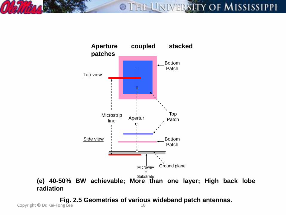
Aperture coupled stacked
patches
(e) 40-50% BW achievable; More than one layer; High back lobe
radiation
Fig. 2.5 Geometries of various wideband patch antennas.
Top view
Side view
Top Patch
Ground plane
Microstrip line
Apertur
e
Bottom Patch
Bottom Patch
Microwave
Substrate

Copyright © Dr. Kai-Fong Lee 17
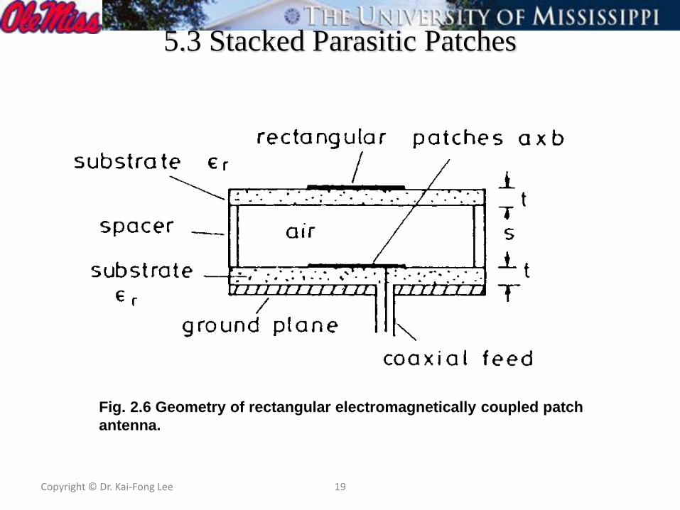
5.3 Stacked Parasitic Patches
The stacked patch arrangement, consisting of one fed patch on one
layer and a parasitic patch on another layer, is one of the most
popular wideband microstrip antenna. The parasitic patch introduces
a second resonance. Many authors have contributed to the study of
this design [A. Sabban, 1983; C. H. Chen et al. 1984; Lee, Lee and
Bobinchak, 1987; Barlatey et al. 1990; Tulintseff at al. 1991].
Example 1: R. Q. Lee, K. F. Lee, J. Bobinchak, Electronics Letters,
Vol. 23, pp. 1070 – 1072, 1987.
This paper, the first Journal paper on the subject, reported an
experimental study of the geometry shown in Fig.2.6. A patch
antenna with a parasitic patch is sometimes known as an
electromagnetically coupled patch antenna. The experiment was
performed at NASA Lewis Research Center (later renamed Glenn
Research Center) by my MS student J. Bobinchak, in collaboration
with Dr. R. Q. Lee of NASA.

Dr. Kai Fong Lee and Dr. Richard Q. Lee at NASA Lewis Research Center, Summer 1986
18
Copyright © Dr. Kai-Fong Lee 19
5.3 Stacked Parasitic Patches
Fig. 2.6 Geometry of rectangular electromagnetically coupled patch
antenna.

Copyright © Dr. Kai-Fong Lee 20
5.3 Stacked Parasitic Patches
Table 2.2 Characteristics of a rectangular electromagnetically coupled patch
antenna.

Copyright © Dr. Kai-Fong Lee 21
5.3 Stacked Parasitic Patches
Fig. 2.7 Patterns of a rectangular electromagnetically coupled patch antenna.
a = 1.5 cm, b = 1 cm, r = 2.17, t = 0.0254 cm, s = 0.0508 cm (region 1), 0.61 cm
(region 2) and 0.9 cm (region 3).
Patterns of a single patch are also shown (solid curves).
Copyright © Dr. Kai-Fong Lee 22
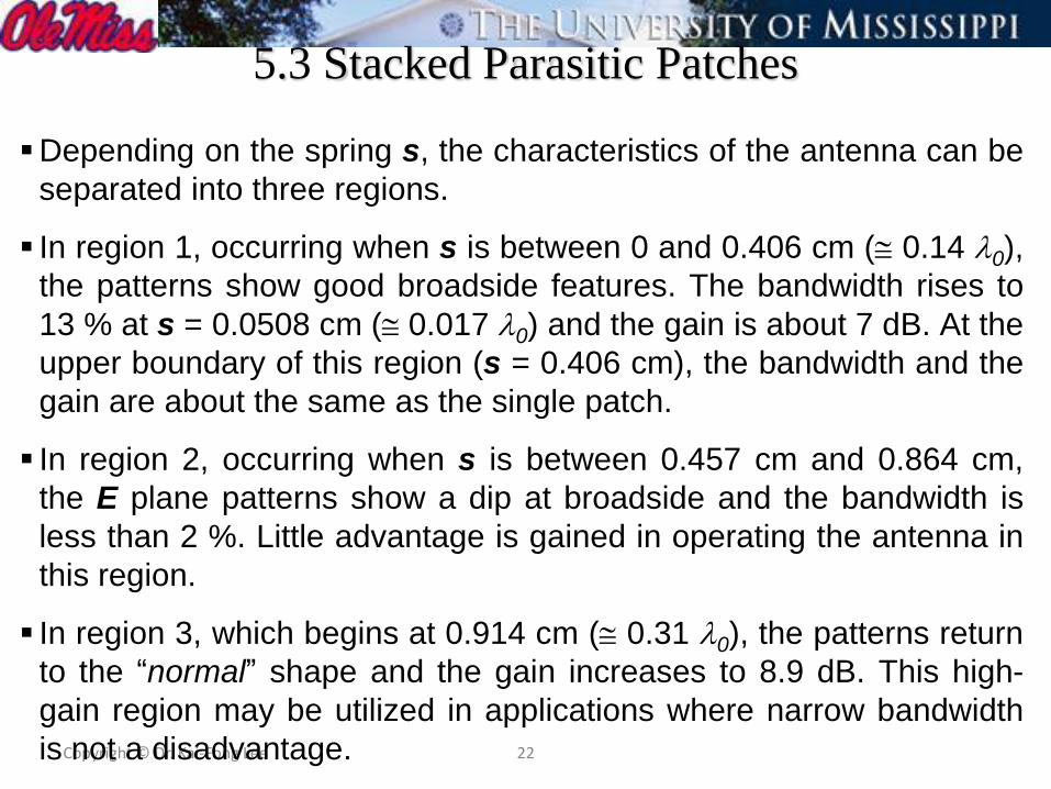
5.3 Stacked Parasitic Patches
Depending on the spring s, the characteristics of the antenna can be
separated into three regions.
In region 1, occurring when s is between 0 and 0.406 cm ( 0.14 0),
the patterns show good broadside features. The bandwidth rises to
13 % at s = 0.0508 cm ( 0.017 0) and the gain is about 7 dB. At the
upper boundary of this region (s = 0.406 cm), the bandwidth and the
gain are about the same as the single patch.
In region 2, occurring when s is between 0.457 cm and 0.864 cm,
the E plane patterns show a dip at broadside and the bandwidth is
less than 2 %. Little advantage is gained in operating the antenna in
this region.
In region 3, which begins at 0.914 cm ( 0.31 0), the patterns return
to the “normal” shape and the gain increases to 8.9 dB. This high-
gain region may be utilized in applications where narrow bandwidth
is not a disadvantage.

Copyright © Dr. Kai-Fong Lee 23
5.3 Stacked Parasitic Patches
Example 2: K. F. Lee, W. Chen, R. Q. Lee, Microwave and Optical
Technology Letters, Vol. 8, No. a, pp. 212 – 215, 1995.
Subsequent to the 1987 paper, my student W. Chen developed a full-wave moment
method analysis and a computer program for multi-layer microstrip antennas. Using
this program, representative design guides for the configuration of Fig.35, operating
at the center frequency of 5 GHz, are shown in Table 3. In Table 3, design 1 gives
the parameters which achieve a bandwidth of 12% for the case when there is no
superstrate (dielectric cover). When a superstrate of thickness 0.26 mm and relative
permittivity of 2.2 is placed on the top of the parasitic patch, the parameters which
yield 12% impedance bandwidth are given in design 2. Design 3 provides the
antenna parameters which result in a bandwidth of 15% when no superstrate is
present. If the center frequency is changed, it is only necessary to scale the length
parameters accordingly (patch dimensions, substrate and superstrate thickness,
feed location).
The patterns of stacked patches are stable across the impedance bandwidth. Typical
E and H plane half-power bandwidths are 760 and 860 respectively. This is to be
compared with 920 and 860 for the single patch. The gain of the stacked patches is
about 6.0 dBi and that of the single patch is about 5.2 dBi.

Copyright © Dr. Kai-Fong Lee 24
5.3 Stacked Parasitic Patches
Table 2.3 Design examples for stacked electromagnetically
coupled patch antennas at the center frequency of 5 GHz.
Fig. 2.8 Stacked lectromagnetically
coupled patch antenna with superstrate

Copyright © Dr. Kai-Fong Lee 25
5.3 Stacked Parasitic Patches
Fig. 2.9 Impedance loci for a stacked EMCP antenna with the parameters given by Set
1 of Table 2.3. Bandwidth = 12 %.

Copyright © Dr. Kai-Fong Lee 26
5.3 Stacked Parasitic Patches
Fig. 2.10 Impedance loci for a stacked
EMCP antenna with the parameters given
by Set 2 of Table 2.3. Bandwidth = 12 %.
Fig. 2.11 Impedance loci for a stacked
EMCP antenna with the parameters given
by Set 3 of Table 2.3. Bandwidth = 15 %.
Stacked patch designs seldom exceed 20 % BW.

Copyright © Dr. Kai-Fong Lee 27
References on section 5.1-5.3
W. Chen, K. F. Lee and R. Q. Lee, “Input Impedance of Coaxially Fed
Rectangular Microstrip Antenna on Electrically Thick Substrate,” Microwave and
Optical Technology Letters, Vol. 6, No. 6, pp. 387-390, 1993.
W. Chen, K. F. Lee and R. Q. Lee, “Spectral-Domain Moment-Method Analysis
of Co-planar Microstrip Parasitic Subarrays,” Microwave and Optical
Technology Letters, Vol. 6, No. 3, pp. 157-163, 1993.
C. Wood, “Improved Bandwidth of Microstrip Antennas Using Parasitic
Elements,” IEE Proc., Pt. H, Vol. 127, pp. 231-234, 1980.
J. R. Mosig and F. Gardiol, “The Effect of Parasitic Elements on Microstrip
Antennas,” IEEE AP-S International Symposium Digest, pp. 397-400, 1985.
C. K. Aanandan, P. Mohanabm, and K. G. Nair, “Broad-Band Gap Coupled
Antenna,” IEEE Trans. Antennas Propagat., Vol. AP-38, No. 10, pp. 1581-1586,
1990.
K. C. Gupta, “Multiport Network Approach for Modelling and Analysis of
Microstrip Patch Antenna and Arrays,” in J. R. James and P. S. Hall (Editors),
Handbook of Microstrip Antennas, Peter Peregrinus, London, 1989.

Copyright © Dr. Kai-Fong Lee 28
References on stacked patches
A. Sabban, “New broadband stacked two-layer microstrip antenna,” IEEE AP-
Symposium Digest, pp. 63-66, 1983.
L. J. Barlately, J. R. Mosig, and T. Sphicopoulos, “Analysis of stacked microstrip
patches with a mixed potential integral equation,” IEEE Trans. Antennas
Propagat., Vol. AP-38, pp. 608-615, 1990.
R. Q. Lee, K. F. Lee, and J. Bobinchak, “Characteristics of a two-layer
electromagnetically coupled rectangular patch antenna,” Electronics Letters, Vol.
23, No. 20, pp. 1070-1073, 1987.
A. N. Tulintseff, S. M. Ali and J. A. Kong, “Input impedance of a probe-fed
stacked circular microstrip antenna,” IEEE Trans. Antennas and Propagat., Vol.
AP-39, pp. 382-390, 1991.
K. F. Lee, W. Chen, R. Q. Lee, “Studies of stacked electromagnetically coupled
patch antenna,” Microwave and Optical Technology Letters, Vol. 8, No. 4, pp.
212-215, 1995.

Copyright © Dr. Kai-Fong Lee 29
5.4 Aperture Coupled Patches
5.4.1 Introduction
This feeding method was proposed by Pozar (1985). The feed
consists of an open-ended microstrip that is located on a dielectric
slab below the ground plane. The microstrip antenna is formed on a
separate dielectric slab above the ground plane and the two
structures are electromagnetically coupled through an electrically
small aperture in the ground plane between them. In the original
paper by Pozar, the aperture was in the form of a small circular hole
(Fig.2.12). Subsequently, a more common shape of the aperture was
in the form of a narrow rectangular slot.
Professor D. M. PozarUniversity of Massachusetts
Amherst

Copyright © Dr. Kai-Fong Lee 30
5.4 Aperture Coupled Patches
Fig. 2.12 Side view (a) and top view (b) of a rectangular microstrip
antenna aperture coupled to a microstripline.
Copyright © Dr. Kai-Fong Lee 31
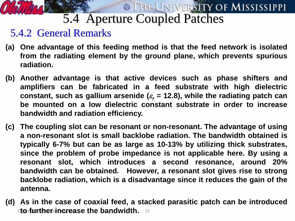
5.4 Aperture Coupled Patches5.4.2 General Remarks
(a) One advantage of this feeding method is that the feed network is isolated
from the radiating element by the ground plane, which prevents spurious
radiation.
(b) Another advantage is that active devices such as phase shifters and
amplifiers can be fabricated in a feed substrate with high dielectric
constant, such as gallium arsenide (r = 12.8), while the radiating patch can
be mounted on a low dielectric constant substrate in order to increase
bandwidth and radiation efficiency.
(c) The coupling slot can be resonant or non-resonant. The advantage of using
a non-resonant slot is small backlobe radiation. The bandwidth obtained is
typically 6-7% but can be as large as 10-13% by utilizing thick substrates,
since the problem of probe impedance is not applicable here. By using a
resonant slot, which introduces a second resonance, around 20%
bandwidth can be obtained. However, a resonant slot gives rise to strong
backlobe radiation, which is a disadvantage since it reduces the gain of the
antenna.
(d) As in the case of coaxial feed, a stacked parasitic patch can be introduced
to further increase the bandwidth.

Copyright © Dr. Kai-Fong Lee 32
5.4 Aperture Coupled Patches5.4.3 Example of a Wideband Aperture Coupled Patch Antenna
By using a resonant slot and relatively thick foam substrate for the patch,
Croq and Papiernik (1990) reported a VSWR < 1.5 impedance bandwidth of
22%. The antenna geometry and the antenna dimensions are shown in Fig.
2.13. Note that there was a dielectric cover (radome) protecting the patch.
(a) Feed: rf = 2.2; tgd = 0.001; Hf = 0.762mm; Wf = 2.32mm; Ls =
2.85mm
(b) Slot: Aw = 0.8mm; A1 = 15.4mm
(c) Square patch: Wp = 17mm; Hp = 5.5mm; rp = 1
(d) Radome: Hs = 1.6mm; rs= 2.2; tgd = 0.001
Fig. 2.13 Aperture coupled patch antenna

Copyright © Dr. Kai-Fong Lee 33
The measured and computed impedances showed that, in the
frequency range 4.85 to 6.1 GHz, the VSWR was less than 1.5,
corresponding to a bandwidth of about 22%. The antenna gain
was found to be about 8 dB for the entire bandwidth. The
maximum back to front level was about -14 dB at the frequency
of 5.6 GHz and was about -12 dB over the band. The strong
back radiation is a major disadvantage of a resonant slot
aperture coupled patch antenna.

Copyright © Dr. Kai-Fong Lee 34
References on aperture coupled patches
● D. M. Pozar, “Microstrip antenna aperture-coupled to a microstripline,”
Electronics Letters, Vol. 21, pp. 49-50, 1985.
● P. L. Sullivan and D. H. Schaubert, “Analysis of an aperture coupled
microstrip antenna,” IEEE Trans. on Antennas and Propagation, Vol. 34,
No.8, pp. 977-984, 1986.
● F. Crog and A. Papernik, “Large bandwidth aperture-coupled microstrip
antenna,” Electronics Letters, Vol. 26, pp. 1293-1294, 1990.
● S. D. Targonski, R. B. Waterhouse, and D. M. Pozar, “Design of wide-band
aperture-stacked patch microstrip antennas,” IEEE Trans. On Antennas
and Propagation, Vol. 46, No. 9, pp. 1245-1251, 1998.

Copyright © Dr. Kai-Fong Lee
Fig. 2.14 Geometry of the U-Slot Patch Antenna
5.5 The Wideband U-Slot Patch Antenna
5.5.1 General Remarks The U-slot design was first introduced in a rather obscure conference “International
Conference in Radio Science (ICRS)” in Beijing in August 1995 under the invited paper
“Progress in the Search of Wideband Microstrip Antennas” by K. F. Lee and T. Huynh.
The geometry is shown in Fig.2.14.
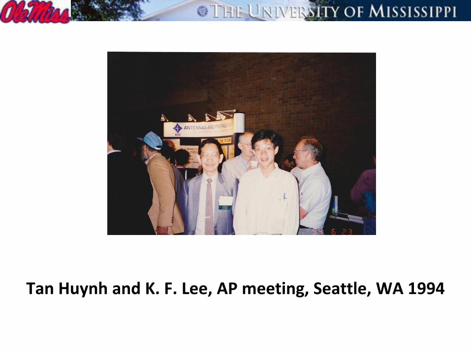
Tan Huynh and K. F. Lee, AP meeting, Seattle, WA 1994
Copyright © Dr. Kai-Fong Lee 37
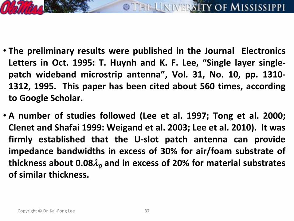
• The preliminary results were published in the Journal ElectronicsLetters in Oct. 1995: T. Huynh and K. F. Lee, “Single layer single-patch wideband microstrip antenna”, Vol. 31, No. 10, pp. 1310-1312, 1995. This paper has been cited about 560 times, accordingto Google Scholar.
• A number of studies followed (Lee et al. 1997; Tong et al. 2000;Clenet and Shafai 1999: Weigand et al. 2003; Lee et al. 2010). It wasfirmly established that the U-slot patch antenna can provideimpedance bandwidths in excess of 30% for air/foam substrate ofthickness about 0.080 and in excess of 20% for material substratesof similar thickness.

Copyright © Dr. Kai-Fong Lee 38
5.5.2 Air/foam substrate
• In the original study of Huynh and Lee, the wide-bandwidth characteristics of theantenna was demonstrated experimentally. It was pointed out in their paper thatthe factors contributing to the wideband behavior were (1) the air substrate; (2) arelative thick substrate (about 0.08 0); (3) the capacitance introduced by the U-slot, which countered the feed inductance; and (4) the additional resonanceintroduced by the U-slot, which combined with the patch resonance to produce abroadband response.
• I was at City University of Hong Kong in the summer of 1995. Prof. Luk assigned K.F. Tong to study the U-slot antenna. In those days, commercial simulationsoftwares were not available. After trying out many dimensions, he settled in twoversions to study experimentally. He also developed a FDTD code for the antenna.The results of one of the antennas are summarized below.

K. F. Tong’s U-slot patch antennas, summer 1997

K. F. Tong and K. F. Lee at University College London 3/2005

Copyright © Dr. Kai-Fong Lee 41
5.5.2 Air/foam Subsrate
Fig. 2.15 VSWR of the U-slot patch antenna with dimensions: W=36
mm, L=26 mm, F=13 mm, Ws=12 mm, Ls=20 mm, a= 2mm, b=4 mm,
cx=cy=2 mm, and h=5 mm. (x measured, — computed)

Copyright © Dr. Kai-Fong Lee 42
5.5.2 Air/foam substrate• The impedance bandwidth was about 30%.
• The measured patters (not shown here) were stable across the band. The E and Hplane beamwidths were about 70 0 and 65 0 respectively. The gain of the antennawas around 7.5 dBi, about 2 dB higher than the traditional patch antenna.
• While the above mentioned studies, as well as others, have shown that more than30% impedance bandwidth can be obtained when an air-substrate thickness ofabout 0.08 0 is used, it should be pointed out that some applications do not needsuch a wide bandwidth. For example, 8.1% is sufficient for Advanced MobilePhone Services (AMPS) while only 8.7% is needed for Global System for MobileCommunications (GSM). While such bandwidths cannot be realized by thetraditional patch antenna, it has been shown (Lee et al. 2010) that these can bemet by a U-slot patch only 0.033 thick, which has a 12% bandwidth.

Copyright © Dr. Kai-Fong Lee 43
5.5.3 Material Subsrate
• Although the first series of studies used an air or foam substrate,subsequent investigations have confirmed that the U-slot widebanddesign can also be implemented with material substrates. Asexpected, the bandwidth of a patch on a material substrate is smallerthan one on an air or foam substrate.
• Tong et al. (2000) presented both experimental study and FDTDanalyses of two U-slot patches with relative permittivity εr=2.32. Thedimensions of one of the antennas are shown in Table 2.4. Theoperating frequencies and bandwidths of this antenna are shown inTable 2.5. The 3 dB-gain bandwidths were about the same as theimpedance bandwidths, and the average gains of the antennas wereabout 7 dBi across the matching band.

εr W L Ws Ls b F cx cy h
2.33 36.0 26.0 14.0 18.0 4.0 13.0 2.0 2.0 6.4
Table 2.4. Dimensions of antenna in millimeters
fl(GHz) fo(GHz) fu(GHz) BW (GHz) BW (%)
Computed 2.87 3.28 3.69 0.82 25.0
Measured 2.76 3.16 3.56 0.80 25.3
Table 2.5. Operating frequencies and bandwidth of the antenna in Table 7

Copyright © Dr. Kai-Fong Lee 45
5.5.4 Variations of the U-slot patch and the E-patch
The U-slot design has been found to yield wideband characteristics for
other patch shapes such as the circular and the triangular patches.
Other shapes for the embedded slot (e.g. V, circular arc, omega) were
found to increase the impedance bandwidth also.
By letting the width of the horizontal slot go to zero and extending the
two vertical slots to the edge of the patch, an E-patch results (Ooi et a.
2000; Yang et al. 2001). This geometry is shown in Fig. 2.16. As in
the U-slot the parallel slots provide an additional path for the currents,
giving rise to a second resonance. The parallel slots can also
introduce a capacitance which compensates for the probe inductance,
thus enabling the use of relatively thick substrate. In Yang et al. 2001,
impedance bandwidths of about 30% were obtained for E patches
operating at the center frequency of around 2.4 GHz, using air
substrate of about 0.080. The antenna parameters for one such
antenna are listed below, in mm: L=70, W=30, h=15, Xf =35, Yf =6, Ls
=40, Ws =6, Ps =10. Ground plane size = 14 cm x 21 cm.
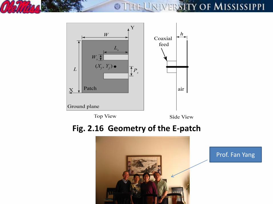
Fig. 2.16 Geometry of the E-patch
Prof. Fan Yang

Copyright © Dr. Kai-Fong Lee 47
References on the U-slot patch
T. Huynh and K. F. Lee, “Single-layer single-patch wideband microstrip
antenna,” Electronics Letters, Vol. 31, No. 16, pp. 1310-1312, 1995.
K. F. Lee, K. M. Luk, K. F. Tong, S. M. Shum, T. Huynh and R. Q. Lee,
“Experimental and simulation studies of the coaxially-fed U-slot
rectangular patch antenna,” IEE Proc.-Microw. Antennas, Propaga., Vol.
144, pp. 354-358, 1997.
K. F. Tong, K. M. Luk, K. F. Lee, and R. Q. Lee, “A broadband U-slot
rectangular patch antenna on a microwave substrate,” IEEE Trans. on
Antennas and Propagation, Vol. 48, Number 6, pp. 954-960, 2000.
K. M. Luk, Y. W. Lee, K. F. Tong, and K. F. Lee, “Experimental studies of
circular patch with slots,” IEE Proc.-Microw. Antennas, Propaga., Vol.
144, No. 6, pp. 421-424, 1997.
S. Weigand, G. H. Huff, K. H. Pan, and J. T. Bernhard, “Analysis and
design of broad-band single-layer rectangular U-slot microstrip patch
antenna,” IEEE Trans. Antennas Propagat., Vol. 51, No. 3, pp. 457-468,
2003.

Copyright © Dr. Kai-Fong Lee 48
K. M. Luk, K. F. Lee and W. L. Tam, “Circular U-slot patch with dielectric
superstrate,” Electronics Letters, Vol. 33, pp. 1001-1002, 1997.
H. Rafi and L. Shafai, “Broadband microstrip patch antenna with V-slot”,
IEE Proc. Microwave, Antennas and Propagat, Vol. 151, No. 3, pp. 435-440,
2004.
B.I.Ooi and Q.Shen,”A novel E-shaped broadband microstrip patch
antenna,” Microwave Opt. Tech. Lett. Vol. 27, No. 5, pp.348-352, 2000.
F. Yang, X. X. Zhang, X. Ye and Y. Rahmat-Samii, “Wideband E-shaped
patch antennas for wireless communications,” IEEE Trans. Antennas and
Propagat., Vol. 49, No. 7, pp. 1094-1100, 2001.
R. Chair, K. F. Lee, C. L. Mak, K. M. Luk and A. A. Kishk, “Miniature
Wideband Half U-Slot and Half E-Shaped Patch Antennas,” IEEE
Transactions on Antennas and Propagation, Vol. 53, No. 8, pp. 2645-2652,
Aug. 2005.
K. F. Lee, S. Yang, A. A. Kishk, and K. M. Luk, “The Versatile U-Slot Patch
Antenna,” IEEE Antennas and Propagation Magazine, Vol. 52, pp. 71-78,
2010.

Copyright © Dr. Kai-Fong Lee 49
5.6 The L-Probe Fed Patch
5.6.1 The L-Probe Fed Patch, Mak et al. (1998)
This design, shown in Fig.44, was first introduced by Luk, Mak, Chow
and Lee (1998). The parallel arm of the probe, being an open line less
than a quarter of a wavelength, presents a capacitance. This
capacitance allows the use of thick substrate because it counteracts
the probe inductance. In conjunction with the inductance of the
perpendicular portion of the probe, a second resonance is created.
This is to be contrasted with the conventional probe, which acts only
as an inductor which causes a mismatch and degrades the bandwidth
performance of the antenna.
Similar to the U-slot patch, this design has only one patch and one
layer. Using foam substrate between 0.08 to 0.10, it achieves 30% or
more matching bandwidth.
Experimental results for the dimensions shown in Fig. 2.17 are given
in Figs. 2.18-2.21.

C. L. Mak in Columbia, Missouri; the other student is John Hawkins
50

Copyright © Dr. Kai-Fong Lee 51
5.6 The L-Probe Fed Patch
5.6.1 The L-Probe Fed Patch, Mak et al. (1998)
Fig. 2.17 Structure of the L-shaped probe fed patch antenna.
Patch
Ground plane
L shaped probe
Feed
H
WL
y
x
z
Plastic post
(a) Perspective view (b) Side view
b
a
D
Parameters W L H b a D
Value /mm 30mm 25mm 6.6mm 10.5mm 5.5mm 2mm
0.44λ0 0.37λ0 0.098λ0 0.156λ0 0.082λ0 0.03λ0

Copyright © Dr. Kai-Fong Lee 52
5.6 The L-Probe Fed Patch
5.6.1 The L-Probe Fed Patch, Mak et al. (1998)
Fig. 2.18 Measured gain and SWR against frequency.
36% (SWR<2)

Copyright © Dr. Kai-Fong Lee 53
5.6 The L-Probe Fed Patch
5.6.1 The L-Probe Fed Patch, Mak et al. (1998)
Fig. 2.19 Measured input impedance against
frequency.
real
------- imaginary

54
SWR and gain
Figure 2.20 Measured gain and SWR against frequency
36% (SWR<2)

55
Radiation patterns
C. L. Mak, K. M. Luk, K. F. Lee, and Y. L. Chow, “Experimental Study of a Microstrip Patch Antenna with an L-shaped Probe,” IEEE Transactions on Antennas
and Propagation, vol. AP-48, No. 5, pp. 777-783, May 2000.
Figure 2.21 Measured radiation patterns at (a) 4GHz (b) 4.53GHz (c)
5.34GHz

Copyright © Dr. Kai-Fong Lee 56
5.6 The L-Probe Fed Patch
5.6.2 Subsequent studies
The paper by Mak et al. (1998) was followed by a more
detailed paper on experimental results (Mak et al. 2000)
and by a FDTD analysis by Guo et al. (2001), both of which
provided some design guides.
Similar to the U-slot patch, this design is not limited to the
rectangular patch. Wideband circular and annular ring
patch antennas with L-probe feed have been reported.
Two related designs are the L-strip and the T-probe fed
patches. A patch fed by a L-strip attained a VSWR <2
bandwidth of 49% while a T-probe fed patch achieved a
bandwidth of 40%.

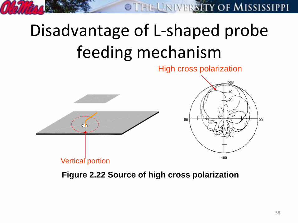
58
Disadvantage of L-shaped probe feeding mechanism
High cross polarization
Vertical portion
Figure 2.22 Source of high cross polarization

5.6.3.1 The M-Probe Fed Patch Antenna (Lai and Luk 2006)
59
5.6.3 The M-Probe/Strip Fed Patch Antenna
Fig. 2.23 Geometry of the meandering probe fed patch antenna.
Parameters L W Hp GL GW g1=g2 h1=h2 s1=s2 ts ws
Value/mm 60 (0.364λ0)
70 (0.425λ0)
17.5 (0.106λ0)
300 (1.82λ0)
200 (1.21λ0)
1.5 (0.01λ0)
9.5 (0.06λ0)
20.5 (0.123λ0)
0.2 (0.0012λ0)
9.5 (0.06λ0)
(c)
s1
h1
h2
s2ws
(a)
(b)
Hp
Hp
g1
g2
W
L
Meandering probe
SMA Connector
Patch
Screw
x
z
y
y
xz
z
y
x
Ground plane
ts
SM
A
Con
ne
cto
r
Connecting position
Patc
hFoam Spacer
x
z y
L
W
GL
G
W
Ground planews
Connect to
SMA
Connector
(d)
One method to reduce crosspolarization is to modify the L-probe into a meandering probe
as shown in Fig.2.23.

With Dr. H. W. Lau and Dr. H. Wong
Paris, October 2005

61
Current Distribution
Low cross polarization level
180º phase difference of the current on the Meandering probe
Patch
Finite ground plane
Meandering probe
Coaxial feed
Figure 2.24 Side view of the current vector density
62
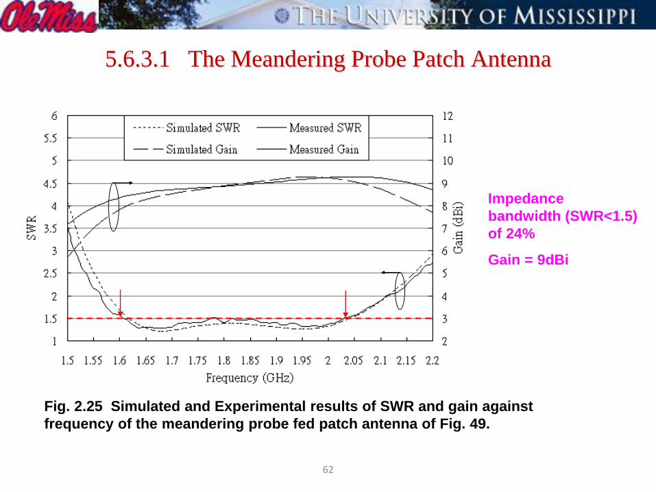
5.6.3.1 The Meandering Probe Patch Antenna
Fig. 2.25 Simulated and Experimental results of SWR and gain against
frequency of the meandering probe fed patch antenna of Fig. 49.
Impedance
bandwidth (SWR<1.5)
of 24%
Gain = 9dBi
63
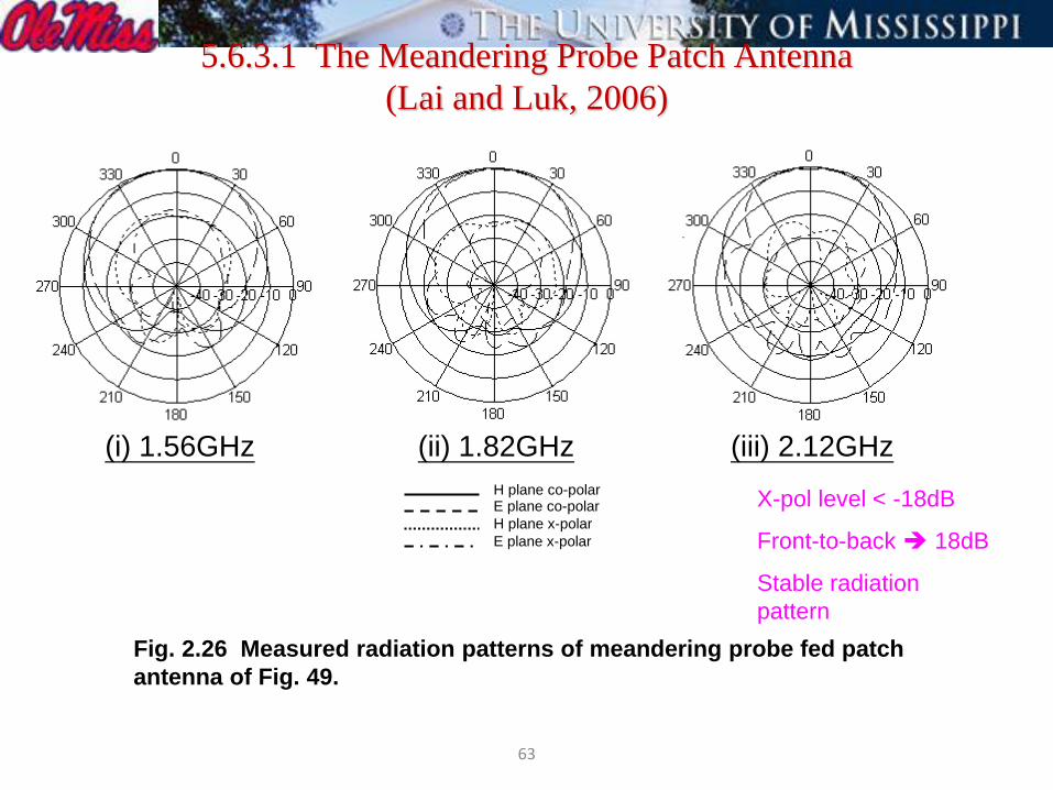
5.6.3.1 The Meandering Probe Patch Antenna
(Lai and Luk, 2006)
H plane co-polarE plane co-polar
H plane x-polar
E plane x-polar
Fig. 2.26 Measured radiation patterns of meandering probe fed patch
antenna of Fig. 49.
(i) 1.56GHz (ii) 1.82GHz (iii) 2.12GHz
X-pol level < -18dB
Front-to-back 18dB
Stable radiation
pattern

64
5.6.3.2 The Meandering Strip Fed Patch Antenna (Lai and Luk 2008)The fabrication process is simplified if the meandering feed is fabricated on a printd circuit board, forming
a printed meandering strip (PMS)
Soldering between the PMS and the patch
Finite Microwave Substrate (εr=4.6)
Patch
Foam Space
r
x
zy
L
W
GL
GW
Finite Ground PlaneConnect to SMA
Launcher
t
(a) Perspective
view
(b) Side view
hg
dL
L
H
h
g
Finite Ground
Plane
PMS with 2mm width
Finite Microwave Substrate
SMA launcher
Soldering pointPatc
h
y
z
x
Finite Ground
Plane(c) Front view
Soldering point
W
H PMS with 2mm width
Finite Microwave Substrate
SMA launcher
Patc
h t
x
z
y
Parameters W L Hp dL H g h t
Values/mm 70 60 16.5 40 16.5 2 12.5 1.5
(0.427λ0) (0.366λ0) (0.101λ0) (0.244λ0) (0.101λ0) (0.122λ0) (0.76λ0) (0.009λ0)
Fig. 2.27 Geometry of the printed meandering strip fed patch
antenna.

Copyright © Dr. Kai-Fong Lee 65
5.6.3.2 The Meandering Strip Patch Antenna
Fig. 2.28 Simulated and experimental results of SWR and gain against
frequency of the printed meandering strip fed patch antenna of Fig. 53.
11.11.21.31.41.51.61.71.81.9
22.12.2
1.6 1.65 1.7 1.75 1.8 1.85 1.9 1.95 2 2.05 2.1
Frequency (GHz)
SW
R
0
2
4
6
8
10
12
Gai
n (d
Bi)
Measured Simulated
22%

Copyright © Dr. Kai-Fong Lee 66
5.6.3.2 The Meandering Strip Patch Antenna
SimulatedMeasured
Fig. 2.29 Radiation patterns of printed meandering strip fed patch antenna at
1.8GHz.
H plane co-polarE plane co-polar
H plane x-polar
E plane x-polar
X-pol level < -28dB
Front-to-back
20dB
Stable radiation
pattern

Copyright © Dr. Kai-Fong Lee 67
Section 5.6 references
● K. M. Luk, C. L. Mak, Y. L. Chow, and K. F. Lee , “Broadband microstrip patch antenna,”
Electronics Letters, Vol. 34, pp. 1442-1443, 1998.
● C. L. Mak, K. M. Luk, K. F. Lee, and Y. L. Chow, “Experimental study of a microstrip patch
antenna with an L-shaped probe,” IEEE Trans. Antennas and Propagation, Vol. 48, No. 5, pp.
777-783, 2000.
● Y. X. Guo, C. L. Mak, K. M. Luk and K.F. Lee “Analysis and design of L-probe proximity fed-patch
antennas,” IEEE Trans. Antennas and Propagation, Vol. 49, No. 2, pp. 145-149, 2001.
● C. L. Mak, H. Wong, and K. M. Luk, “High-Gain and Wide-Band Single-Layer patch antenna for wireless communications,” IEEE Transactions on Vehicular Technology, Vol. 54, No. 1, pp. 33-40, January 2005.
● C. L. Mak, H. Wong, and K. M. Luk, “High-Gain and Wide-Band Single-Layer Patch Antenna for wireless communications,” IEEE Transactions on Vehicular Technology, vol. 54, No. 1, pp. 33-40, January 2005.
● K. M. Luk, C. L. Mak, Y. L. Chow and K. F. Lee, “Broadband circular patch antenna with a L-
shaped probe,” Microwave and Optical Technology Letters, Vol. 20, No. 4, pp. 256-257, 1999.
● C. L. Mak, K. M. Luk, and K. F. Lee, “Microstrip line-fed L-strip patch antenna,” IEE Proceedings-
Microwaves, Antennas and Propagation, Vol. 146, No. 4, pp. 282-284, 1999.

Copyright © Dr. Kai-Fong Lee 68
● C. L. Mak, K. F. Lee, and K. M. Luk, “Broadband patch antenna with a T-shaped probe,” IEE
Proceedings-Microwave, Antennas, Propagation, Vol. 147, No. 2, pp. 73-76, April, 2000.
● H. W. Lai and K. M. Luk, “Design and study of wide-band patch antenna fed by
meandering probe,” IEEE Trans. Antennas Propagat., Vol. 54, pp. 564-571, 2006.
● H. W. Lai and K. M. Luk, “Wideband patch antenna fed by printed meandering strip,” Microwave
and Optical Technlogy Letters, Vol. 20, No. 4, pp. 256-257, 2008.

Copyright © Dr. Kai-Fong Lee 69
6. Full wave analysis and CAD formulas
As mentioned previously, the cavity model was limited to the basic
structure of a single patch of regular shape on a grounded
substrate. It became inaccurate for substrate thickness
exceeding about 0.03 free space wavelength and is unable to
analyze many practical geometries such as patch with
dielectric cover, patch with slots, or multiple patches in single
or multi-layers. These have to be handled with full wave
analysis, i.e. solving Maxwell’s equations subject to the
boundary conditions at hand. While papers based on full wave
analysis were being published from mid-1980’s through mid-
1990’s, simulation softwares, as as IE3D, HFSS etc were not
commercially available until the late 1990’s. Graduate students,
under the direction of their professors, often had to develop full
wave equations and computer programs for their problem at
hand.

70
6. Full wave analysis and CAD formulas
6.1 Full wave analysis developed in house
Under Prof. K. M. Luk
W. Y. Tam, T. M. Au, S. M. Shum: Moment method
Problems studied: Stacked patches, both fed by coax and by
aperture coupling
K. F. Tong: FDTD
Problem studied: U-Slot Patch
Y. X. Guo: FDTD
Problem studied: L-probe patch

71
6. Full wave analysis and CAD formulas
6.1 Full wave analysis developed in house
Under Prof. K. F Lee
Wei Chen: Moment method
Problems studied: Patch on thick substrate; Wideband
stacked patches, Coplanar parasitic patches; Patch on multi-
layer dielectrics; CAD formula for resonant frequencies of
equitriangular patch
Zhibo Fan: Moment method
Problems studied: Patch with air gap; Dual-frequency
stacked patches; Patch with dielectric cover
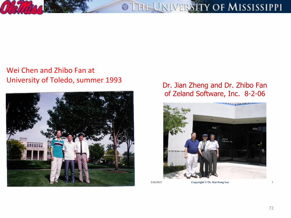
Wei Chen and Zhibo Fan at University of Toledo, summer 1993
72
5/26/2015 Copyright © Dr. Kai-Fong Lee 1
Dr. Jian Zheng and Dr. Zhibo Fanof Zeland Software, Inc. 8-2-06

Copyright © Dr. Kai-Fong Lee 73
Some of our papers using full wave analysis
● Z. Fan and K. F. Lee, “Hankel transform domain analysis of dual-frequency
stacked circular-disk and annular-ring microstrip antennas,” IEEE Trans.
Antennas Propagat., Vol. AP-39, pp. 867-870, 1991.
● Z. Fan and K. F. Lee, “Input impedance of rectangular microstrip antennas
with a dielectric cover,” Microwave and Optical Tech. Letters., Vol. 5, pp. 123-
125, March 1992.
● Z. Fan and K. F. Lee, “Spectral domain analysis of rectangular microstrip
antennas with air gap,” Microwave and Optical Tech. Letters., Vol. 5, pp. 315-
318, June 1992.
● Z. Fan and K. F. Lee, “Input impedance of circular-disk microstrip antennas
with a dielectric cover ,” Microwave and Optical Tech. Letters., Vol. 5, pp. 701-
704, Dec. 1992.
● W. Chen, K. F. Lee and J. Dahele, Theoretical and experimental studies of the
resonant frequencies of equilateral triangular patch antennas, IEEE
Transactions on Antennas and Propagation, Vol. 40, No. 10, pp. 1253-1256,
1992.

Copyright © Dr. Kai-Fong Lee 74
Some of our papers using full wave analysis (continued)
● W. Chen, K. F. Lee and R. Q. Lee, Spectral domain moment method analysis of
coplanar microstrip parasitic subarrays, Microwave and Optical Technology
Letters, Vol. 6(3), pp. 157-163, March 1993.
● W. Chen, K. F. Lee and R. Q. Lee, Input impedance of coaxially-rectangular
microstrip antennas on electrically thick substrate, Microwave and Optical
Technology Letters, Vol. 6(6), pp. 387-390, May 1993.
● W. Chen, K. F. Lee, J.S. Dahele, R. Q. Lee, “CAD formulas for resonant
frequencies of TM01 and TM10 modes of rectangular patch antenna with
superstrate, Journal of Microwave and Millimeter Wave Computer Aided
Engineering, Vol. 3, pp. 340-349, 1993.
● K. F. Lee and Z. Fan, CAD formulas for resonant frequencies of TMII mode of
circular patch antenna with or without superstrate, Microwave and Optical
Technology Letters, Volume 7, No. 12, pp. 570-573. 1994.

Some of our papers using full wave analysis (continued)
● W. Chen, K. F. Lee, R. Q. Lee, Spectral domain full-wave analysis of the input
impedance of coaxially-fed rectangular microstrip antennas, Journal of
Electromagnetic Waves and Applications, Vol. 8, No. 2, pp. 249-272, 1994.
● T.M. Au, K.F. Tong, K.M. Luk and K.F. Lee, “Analysis of aperture-coupled
microstrip antenna and array with an airgap,” IEE Proc. - Microw. Antennas
Propag., Vol. 142, No. 6, pp. 485-488, 1995.
● K. M. Luk, T. M. Au, K. F. Tong, K. F. Lee, “Aperture-coupled multilayer
microstrip antennas,” Chapter 3 in Advances in Microstrip and Printed
Antennas, K. F. Lee and W. Chen (Editors), Wiley Interscience, 1997.
6.2 Microstrip Antenna Development Procedure with the aid of Commercially available simulation softwares
The main motivation of the full wave analysis and softwares developed by Prof. Luk’s group and my group were to verify the measured results of the patch antennas we studied – stacked patches, U-slot patch, L-probe fed patch etc., configurations which cannot be analyzed using the cavity model. Other groups were doing similarly work. In the late 1980’s and early 1990’s, two Ph.D. graduates of the University of Colorado marketed their simulation softwares commercially. Doris Wu marketed “Ensemble” through her company “Boulder Microwaves” (later sold to Ansoft). Jian Zheng marketed “IE3D” through his company “Zeland”, which were later sold to “Mentor Graphics”. Zhibo Fan, who wrote many papers with me, worked in Zeland and is still with Mentor Graphics.
At present, there are numerous electromagnetic simulation softwares in the market.

Copyright © Dr. Kai-Fong Lee 77
Table 2.6 Some commercially available microstrip antenna CAD tools
AnsoftFinite elementHFSS
ZelandFDTDFidelity
CSTFDTDMicrowave Studio
(MAFIA)
Microstrip Designs, Inc.SegmentationMicropatch
Antenna Design Associates,
Inc.Cavity modelPCAAD
EMSSMoment methodFEKO
EMAGMoment method /
GeneticPiCasso
SonnetMoment methodEM
HPMoment methodMomentum
Mentor Graphic/ZelandMoment methodIE3D
AnsoftMoment methodEnsemble
CompanyTheoretical modelSoftware name

6.2 Microstrip Antenna Development Procedure with the aid of commercially available simulation softwares
Design
Specifications
Antenna
Designer
Patch Antenna
Principles and
Design
Techniques
Creativity and
Innovation
Preliminary
Design
Specifications
Commercial or
Self-Developed
Electromagnetic
Simulation
Software
Simulation
Results
Do the
simulation
results agree
well with design
specifications?
Design
Fabrication
Measurement
Results
Do the
measured results
agree well with
design
specifications?
Feedback correction
Feedback correction
Final Design
No
Yes
NoYes


![Electrically Small Antenna Design - ITS Small Antenna Design ... Example : microstrip patch antenna Ground plane ... Bandwidth [MHz] relative patch size f r =1 GHz](https://img.dokumen.tips/doc/110x75/5aa70bfa7f8b9a6d5a8bcb7d/electrically-small-antenna-design-its-small-antenna-design-example-microstrip.jpg)