Embed Size (px)
Citation preview

Organic Electronics 13 (2012) 3326–3332
Contents lists available at SciVerse ScienceDirect
Organic Electronics
journal homepage: www.elsevier .com/locate /orgel
On the scaling behavior of organic ferroelectric copolymer PVDF-TrFEfor memory application
Saptarshi Das ⇑, Joerg AppenzellerDept. of Electrical and Computer Engineering and Birck Nanotechnology Center, Purdue University, West Lafayette, IN 47907, United States
a r t i c l e i n f o a b s t r a c t
Article history:Received 10 August 2012Received in revised form 15 September2012Accepted 23 September 2012Available online 26 October 2012
Keywords:Organic ferroelectricNon-volatile memoryField effect transistorScaling
1566-1199/$ - see front matter � 2012 Elsevier B.Vhttp://dx.doi.org/10.1016/j.orgel.2012.09.036
⇑ Corresponding author.E-mail address: [email protected] (S. Das).
We report an interesting scaling trend in the switching time and the switching voltage ofthe organic ferroelectric copolymer PVDF-TrFE as a function of the device area. We havefound that shrinking the lateral dimensions of the ferroelectric film results in a dramaticdecrease in the switching time and the switching voltage. The phenomenological theory,that explains this abnormal scaling trend, involves in-plane interaction of the polymericchains of the two-dimensional Langmuir–Blodgett (LB) films of the copolymer PVDF-TrFEinterchain and intrachain coupling results in a weak power-law dependence of the switch-ing field on the device area ðESW aA0:1
CH Þ which is ultimately responsible for the decrease inthe switching time and switching voltage. For this scaling study we have used the organicferroelectric copolymer as the top gate dielectric of a field-effect transistor structure withpoly silicon nanowires as channel material. The gated channel area was varied by morethan two orders of magnitude (0.04 –5 lm2) while the thickness of the ferroelectric copoly-mer film was kept constant at 100 nm. Our findings are believed to be of importance toboth, the fundamental understanding of non-equilibrium processes in correlated con-densed matter systems and the technological use of ferroelectric copolymers for non vol-atile memory applications.
� 2012 Elsevier B.V. All rights reserved.
1. Introduction
Ferroelectric materials [1,2] are characterized by twostable spontaneous polarization states which can beswitched by an appropriate external electric field. Thesematerials are therefore an excellent choice for binary codebased nonvolatile random access memory (NVRAM) appli-cations [3,4]. The organic ferroelectric copolymer poly-vinylidene-di-fluoride-tri-fluoro-ethylene (PVDF-TrFE) [5–11] has attracted a considerable amount of attention in thiscontext for next generation NVRAM technologies due to itsexcellent processability, low annealing temperature andtremendous flexibility. Organic copolymers can be inte-grated with both conventional CMOS technology andemerging organic material based microelectronic technol-ogy. However the major road block in the realization of
. All rights reserved.
PVDF based NVRAM lies in the high switching voltage ofthis material. The switching voltage for any ferroelectricmaterial is the product of the switching field and the thick-ness of the ferroelectric layer. Thus, the switching voltagecan be reduced by scaling the thickness of the ferroelectriclayer. However, the switching field (ESW) itself scales in-verse with the thickness ðESW a t�2=3
ox Þ [12,13] making it ex-tremely difficult to scale down the switching voltage(VSW ¼ ESWtox ¼ ct1=3
ox , c being constant) just by reducingthe thickness of the ferroelectric layer. Through our exper-iments we have found that the switching voltage for a100 nm copolymer film is around 15 V and therefore 5 Voperation would require a 4 nm ultra-thin copolymer filmusing the thickness scaling law of the switching voltagementioned above. Controlling the leakage current densityand surface roughness of such an ultra-thin copolymer filmcan be expected to be extremely demanding. In this articlewe will discuss our findings that indicate an alternativeroute to reduce the required switching voltage, namely
S. Das, J. Appenzeller / Organic Electronics 13 (2012) 3326–3332 3327
by shrinking the gated device area. Our experimental datasuggest that the switching field (ESW) for the ferroelectriccopolymer PVDF-TrFE scales as a function of the devicearea ðESW aA0:1
CHÞ and thereby allows to reduce the switchingvoltage at a given oxide thickness. The origin of such anabnormal scaling trend lies according to our phenomeno-logical theory in the long range interchain and intrachaininteraction of the polymeric chains of the two dimensionalLangmuir–Blodgett (LB) films of the copolymer PVDF-TrFE[14–16]. Moreover, we conclude from the experimentallyfound rather large switching times of 500 ns even for thesmallest device dimensions (200 nm � 200 nm) that theswitching process involves domain nucleation rather thandomain wall motion [17,18].
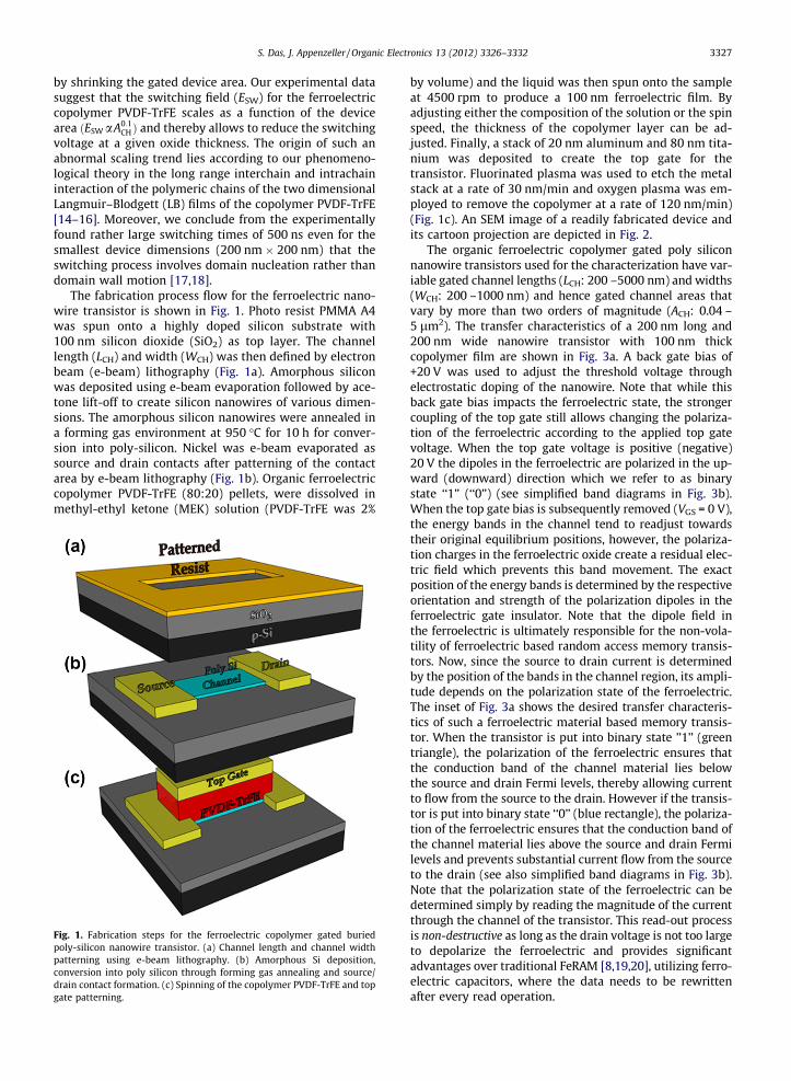
The fabrication process flow for the ferroelectric nano-wire transistor is shown in Fig. 1. Photo resist PMMA A4was spun onto a highly doped silicon substrate with100 nm silicon dioxide (SiO2) as top layer. The channellength (LCH) and width (WCH) was then defined by electronbeam (e-beam) lithography (Fig. 1a). Amorphous siliconwas deposited using e-beam evaporation followed by ace-tone lift-off to create silicon nanowires of various dimen-sions. The amorphous silicon nanowires were annealed ina forming gas environment at 950 �C for 10 h for conver-sion into poly-silicon. Nickel was e-beam evaporated assource and drain contacts after patterning of the contactarea by e-beam lithography (Fig. 1b). Organic ferroelectriccopolymer PVDF-TrFE (80:20) pellets, were dissolved inmethyl-ethyl ketone (MEK) solution (PVDF-TrFE was 2%
Fig. 1. Fabrication steps for the ferroelectric copolymer gated buriedpoly-silicon nanowire transistor. (a) Channel length and channel widthpatterning using e-beam lithography. (b) Amorphous Si deposition,conversion into poly silicon through forming gas annealing and source/drain contact formation. (c) Spinning of the copolymer PVDF-TrFE and topgate patterning.
by volume) and the liquid was then spun onto the sampleat 4500 rpm to produce a 100 nm ferroelectric film. Byadjusting either the composition of the solution or the spinspeed, the thickness of the copolymer layer can be ad-justed. Finally, a stack of 20 nm aluminum and 80 nm tita-nium was deposited to create the top gate for thetransistor. Fluorinated plasma was used to etch the metalstack at a rate of 30 nm/min and oxygen plasma was em-ployed to remove the copolymer at a rate of 120 nm/min)(Fig. 1c). An SEM image of a readily fabricated device andits cartoon projection are depicted in Fig. 2.
The organic ferroelectric copolymer gated poly siliconnanowire transistors used for the characterization have var-iable gated channel lengths (LCH: 200 –5000 nm) and widths(WCH: 200 –1000 nm) and hence gated channel areas thatvary by more than two orders of magnitude (ACH: 0.04 –5 lm2). The transfer characteristics of a 200 nm long and200 nm wide nanowire transistor with 100 nm thickcopolymer film are shown in Fig. 3a. A back gate bias of+20 V was used to adjust the threshold voltage throughelectrostatic doping of the nanowire. Note that while thisback gate bias impacts the ferroelectric state, the strongercoupling of the top gate still allows changing the polariza-tion of the ferroelectric according to the applied top gatevoltage. When the top gate voltage is positive (negative)20 V the dipoles in the ferroelectric are polarized in the up-ward (downward) direction which we refer to as binarystate ‘‘1’’ (‘‘0’’) (see simplified band diagrams in Fig. 3b).When the top gate bias is subsequently removed (VGS = 0 V),the energy bands in the channel tend to readjust towardstheir original equilibrium positions, however, the polariza-tion charges in the ferroelectric oxide create a residual elec-tric field which prevents this band movement. The exactposition of the energy bands is determined by the respectiveorientation and strength of the polarization dipoles in theferroelectric gate insulator. Note that the dipole field inthe ferroelectric is ultimately responsible for the non-vola-tility of ferroelectric based random access memory transis-tors. Now, since the source to drain current is determinedby the position of the bands in the channel region, its ampli-tude depends on the polarization state of the ferroelectric.The inset of Fig. 3a shows the desired transfer characteris-tics of such a ferroelectric material based memory transis-tor. When the transistor is put into binary state ’’1’’ (greentriangle), the polarization of the ferroelectric ensures thatthe conduction band of the channel material lies belowthe source and drain Fermi levels, thereby allowing currentto flow from the source to the drain. However if the transis-tor is put into binary state ‘‘0’’ (blue rectangle), the polariza-tion of the ferroelectric ensures that the conduction band ofthe channel material lies above the source and drain Fermilevels and prevents substantial current flow from the sourceto the drain (see also simplified band diagrams in Fig. 3b).Note that the polarization state of the ferroelectric can bedetermined simply by reading the magnitude of the currentthrough the channel of the transistor. This read-out processis non-destructive as long as the drain voltage is not too largeto depolarize the ferroelectric and provides significantadvantages over traditional FeRAM [8,19,20], utilizing ferro-electric capacitors, where the data needs to be rewrittenafter every read operation.

Fig. 2. SEM images and 3-D cartoon projection of a copolymer gated poly-silicon nanowire transistor. (a) Source/drain contacts to the nanowire. (b) Thecompleted transistor with copolymer as top gate dielectric.
Fig. 3. (a) Transfer characteristics of the copolymer gated silicon nanowire transistor (inset shows the ideal transfer characteristics desired for memoryapplication). (b) Energy band diagram for the same transistor at different operating states.
1 The time constant of the measurement setup was 10 ns (much smallerthan the lowest switching time) and hence does not limit the switchingtime. The data, therefore, represents intrinsic properties of the ferroelectric.
3328 S. Das, J. Appenzeller / Organic Electronics 13 (2012) 3326–3332
Fig. 4a illustrates the measurement technique em-ployed next to determine the switching time of the ferro-electric copolymer and Fig. 4b shows the correspondingexperimental data for a 200 nm long and 200 nm widenanowire channel transistor. In our approach, every timea set of two pulses was applied – the reference pulse in thistechnique has a constant amplitude of �20 V fortReset = 10 s while the test pulse also has an constant ampli-tude equal to 20 V but a variable pulse duration. The refer-ence pulse resets the polarization state of the ferroelectriccopolymer and hence the source to drain current to a lowvalue. When the pulse duration of the test pulse is lessthan the switching time of the ferroelectric copolymer,the source to drain current remains the same as the refer-ence current level, however, if the pulse duration of thetest pulse becomes more than the switching time, the
source to drain current increases. The transition point asshown in the measurement data in Fig. 4b determinesthe switching time for the ferroelectric copolymer.1 (notethat the memory ratio determined from Fig. 4b (ratio of cur-rent in the two states) is �3 in spite of a current ON/OFF ra-tio of �10 at VGS = 0 V in Fig. 3b. This is a direct consequenceof threshold voltage shift between the measurements and donot have any effect on the intrinsic properties being investi-gated in this article) This technique was repeated for all de-vices and the switching time was plotted as a function of thechannel length for different channel widths as shown inFig. 4c. Interestingly both, a reduction in channel width as
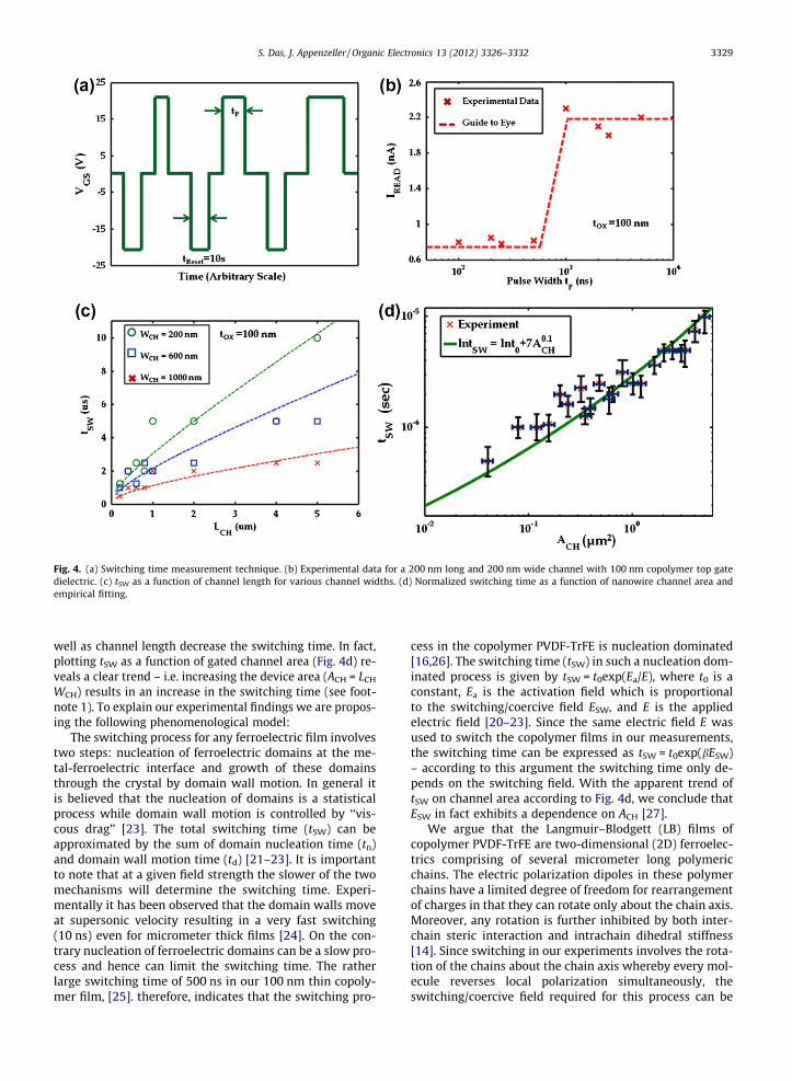
Fig. 4. (a) Switching time measurement technique. (b) Experimental data for a 200 nm long and 200 nm wide channel with 100 nm copolymer top gatedielectric. (c) tSW as a function of channel length for various channel widths. (d) Normalized switching time as a function of nanowire channel area andempirical fitting.
S. Das, J. Appenzeller / Organic Electronics 13 (2012) 3326–3332 3329
well as channel length decrease the switching time. In fact,plotting tSW as a function of gated channel area (Fig. 4d) re-veals a clear trend – i.e. increasing the device area (ACH = LCH
WCH) results in an increase in the switching time (see foot-note 1). To explain our experimental findings we are propos-ing the following phenomenological model:
The switching process for any ferroelectric film involvestwo steps: nucleation of ferroelectric domains at the me-tal-ferroelectric interface and growth of these domainsthrough the crystal by domain wall motion. In general itis believed that the nucleation of domains is a statisticalprocess while domain wall motion is controlled by ‘‘vis-cous drag’’ [23]. The total switching time (tSW) can beapproximated by the sum of domain nucleation time (tn)and domain wall motion time (td) [21–23]. It is importantto note that at a given field strength the slower of the twomechanisms will determine the switching time. Experi-mentally it has been observed that the domain walls moveat supersonic velocity resulting in a very fast switching(10 ns) even for micrometer thick films [24]. On the con-trary nucleation of ferroelectric domains can be a slow pro-cess and hence can limit the switching time. The ratherlarge switching time of 500 ns in our 100 nm thin copoly-mer film, [25]. therefore, indicates that the switching pro-
cess in the copolymer PVDF-TrFE is nucleation dominated[16,26]. The switching time (tSW) in such a nucleation dom-inated process is given by tSW = t0exp(Ea/E), where t0 is aconstant, Ea is the activation field which is proportionalto the switching/coercive field ESW, and E is the appliedelectric field [20–23]. Since the same electric field E wasused to switch the copolymer films in our measurements,the switching time can be expressed as tSW = t0exp(bESW)– according to this argument the switching time only de-pends on the switching field. With the apparent trend oftSW on channel area according to Fig. 4d, we conclude thatESW in fact exhibits a dependence on ACH [27].
We argue that the Langmuir–Blodgett (LB) films ofcopolymer PVDF-TrFE are two-dimensional (2D) ferroelec-trics comprising of several micrometer long polymericchains. The electric polarization dipoles in these polymerchains have a limited degree of freedom for rearrangementof charges in that they can rotate only about the chain axis.Moreover, any rotation is further inhibited by both inter-chain steric interaction and intrachain dihedral stiffness[14]. Since switching in our experiments involves the rota-tion of the chains about the chain axis whereby every mol-ecule reverses local polarization simultaneously, theswitching/coercive field required for this process can be

(a) (b)
(d)(c)
Fig. 5. (a) Switching voltage measurement technique. (b) Experimental data for a 200 nm long and 200 nm wide channel with 100 nm copolymer top gate.(c) Measurement data as a function of different channel lengths at different channel widths. (d) Switching electrical field as a function of nanowire channelarea and fit as discussed in the text.
2 For interpretation of color in Figs. 5 and 6, the reader is referred to theweb version of this article.
3330 S. Das, J. Appenzeller / Organic Electronics 13 (2012) 3326–3332
expected to depend on the area of the film. As the devicearea is increased more polymeric chains couple with oneanother and restrict the molecular motion through inter-chain and intrachain interaction. As a consequence of theshort and long range in-plane coupling the switching en-ergy and therefore the switching field is expected to in-crease with the gated device area. The empiricalrelationship between the switching field and the devicearea we assume follows a power-law dependence of typeESW ¼ ESW0 Ag
CH. Correspondingly, the switching time forthe copolymer can be expressed as tSW ¼ t0 expðlAg
CHÞ,with l being a constant. In order to fit our experimentaldata we have used t0 = 2 ns, l = 7 and g = 0.1 (ACH is inlm2). The relatively small power exponent g indicates thatlong range coupling plays a rather small role which is how-ever enhanced in our switching time measurement due tothe exponential dependence of tSW on ESW.
In order to further support our phenomenological mod-el, we have independently characterized the switchingvoltage as a function of gated channel region. Fig. 5a illus-trates our second measurement approach to determine theswitching voltage of the ferroelectric copolymer andFig. 5b displays the data for a 200 nm long and 200 nmwide nanowire channel transistor with 100 nm copolymer
film as gate oxide. Similar to the technique used to deter-mine the switching time of the ferroelectric copolymer,within every cycle a set of two pulses was applied – thereference pulse which has a constant amplitude of �20 vand a constant pulse duration of 10 s and the actual testpulse which also exhibits a constant pulse duration of10 s but at varying amplitude. The reference pulse resetsthe polarization state of the ferroelectric copolymer andhence the source to drain current (The bottom solid line2
in Fig. 5b). When the amplitude of the test pulse is less thanthe switching voltage of the ferroelectric copolymer, thesource to drain current drops to the reference current levelover time indicating no switching has occurred (dotted bluelines in Fig. 5b). However, if the amplitude of the test pulsebecomes more than the switching voltage, the source todrain current becomes distinctly different from the refer-ence current level and is retained for more than 3 h (solidblue line in Fig. 5b). It is important to note that charges inthe oxide can also give rise to hysteresis in the transfer char-acteristics of a transistor. This is why the initial source to
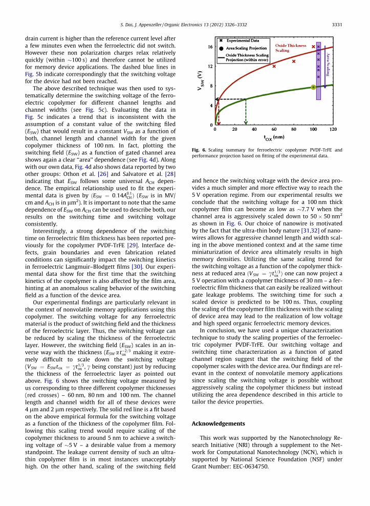
Fig. 6. Scaling summary for ferroelectric copolymer PVDF-TrFE andperformance projection based on fitting of the experimental data.
S. Das, J. Appenzeller / Organic Electronics 13 (2012) 3326–3332 3331
drain current is higher than the reference current level aftera few minutes even when the ferroelectric did not switch.However these non polarization charges relax relativelyquickly (within �100 s) and therefore cannot be utilizedfor memory device applications. The dashed blue lines inFig. 5b indicate correspondingly that the switching voltagefor the device had not been reached.
The above described technique was then used to sys-tematically determine the switching voltage of the ferro-electric copolymer for different channel lengths andchannel widths (see Fig. 5c). Evaluating the data inFig. 5c indicates a trend that is inconsistent with theassumption of a constant value of the switching filed(ESW) that would result in a constant VSW as a function ofboth, channel length and channel width for the givencopolymer thickness of 100 nm. In fact, plotting theswitching field (ESW) as a function of gated channel areashows again a clear ‘‘area’’ dependence (see Fig. 4d). Alongwith our own data, Fig. 4d also shows data reported by twoother groups: Othon et al. [26] and Salvatore et al. [28]indicating that ESW follows some universal ACH depen-dence. The empirical relationship used to fit the experi-mental data is given by ðESW ¼ 0:14A0:1
CHÞ (ESW is in MV/cm and ACH is in lm2). It is important to note that the samedependence of ESW on ACH can be used to describe both, ourresults on the switching time and switching voltageconsistently.
Interestingly, a strong dependence of the switchingtime on ferroelectric film thickness has been reported pre-viously for the copolymer PVDF-TrFE [29]. Interface de-fects, grain boundaries and even fabrication relatedconditions can significantly impact the switching kineticsin ferroelectric Langmuir–Blodgett films [30]. Our experi-mental data show for the first time that the switchingkinetics of the copolymer is also affected by the film area,hinting at an anomalous scaling behavior of the switchingfield as a function of the device area.
Our experimental findings are particularly relevant inthe context of nonvolatile memory applications using thiscopolymer. The switching voltage for any ferroelectricmaterial is the product of switching field and the thicknessof the ferroelectric layer. Thus, the switching voltage canbe reduced by scaling the thickness of the ferroelectriclayer. However, the switching field (ESW) scales in an in-verse way with the thickness (ESW a t�2=3
ox making it extre-mely difficult to scale down the switching voltage(VSW ¼ ESWtox ¼ ct1=3
ox , c being constant) just by reducingthe thickness of the ferroelectric layer as pointed outabove. Fig. 6 shows the switching voltage measured byus corresponding to three different copolymer thicknesses(red crosses) – 60 nm, 80 nm and 100 nm. The channellength and channel width for all of these devices were4 lm and 2 lm respectively. The solid red line is a fit basedon the above empirical formula for the switching voltageas a function of the thickness of the copolymer film. Fol-lowing this scaling trend would require scaling of thecopolymer thickness to around 5 nm to achieve a switch-ing voltage of �5 V – a desirable value from a memorystandpoint. The leakage current density of such an ultra-thin copolymer film is in most instances unacceptablyhigh. On the other hand, scaling of the switching field
and hence the switching voltage with the device area pro-vides a much simpler and more effective way to reach the5 V operation regime. From our experimental results weconclude that the switching voltage for a 100 nm thickcopolymer film can become as low as �7.7 V when thechannel area is aggressively scaled down to 50 � 50 nm2
as shown in Fig. 6. Our choice of nanowire is motivatedby the fact that the ultra-thin body nature [31,32] of nano-wires allows for aggressive channel length and width scal-ing in the above mentioned context and at the same timeminiaturization of device area ultimately results in highmemory densities. Utilizing the same scaling trend forthe switching voltage as a function of the copolymer thick-ness at reduced area ðVSW ¼ ct1=3
ox Þ one can now project a5 V operation with a copolymer thickness of 30 nm – a fer-roelectric film thickness that can easily be realized withoutgate leakage problems. The switching time for such ascaled device is predicted to be 100 ns. Thus, couplingthe scaling of the copolymer film thickness with the scalingof device area may lead to the realization of low voltageand high speed organic ferroelectric memory devices.
In conclusion, we have used a unique characterizationtechnique to study the scaling properties of the ferroelec-tric copolymer PVDF-TrFE. Our switching voltage andswitching time characterization as a function of gatedchannel region suggest that the switching field of thecopolymer scales with the device area. Our findings are rel-evant in the context of nonvolatile memory applicationssince scaling the switching voltage is possible withoutaggressively scaling the copolymer thickness but insteadutilizing the area dependence described in this article totailor the device properties.
Acknowledgements
This work was supported by the Nanotechnology Re-search Initiative (NRI) through a supplement to the Net-work for Computational Nanotechnology (NCN), which issupported by National Science Foundation (NSF) underGrant Number: EEC-0634750.

3332 S. Das, J. Appenzeller / Organic Electronics 13 (2012) 3326–3332
References
[1] J. Valasek, Piezo-electric and allied phenomena in Rochelle salt, Phys.Rev. 17 (1921) 475–481.
[2] J. Valasek, The early history of ferroelectricity, Ferroelectrics 2 (1971)239–244.
[3] Y. Fujisaki, Current status of nonvolatile semiconductor memorytechnology, Jpn. J. Appl. Phys. 49 (2010) 100001–100014.
[4] J.F. Scott, A.P.A. Carlos, Ferroelectric memories, Science 246 (1989)1400–1405.
[5] B. Ploss, F.G. Shin, H.L.W. Chan, C.L. Choy, Pyroelectric activity offerroelectric PT/PVDF-TrFE, IEEE Trans. Dielect. Elect. In. 7 (2000)517–522.
[6] C.G.R. Naber, T. Cristina, W.M.B. Paul, H.G. Gerwin, W.M. Albert, J.T.Fred, S. Sepas, M.L. Dago, High-performance solution-processedpolymer ferroelectric field-effect transistors, Nat. Mater. 4 (2005)243–248.
[7] Y.S. Jong, R. Sangwoo, C.P. Yoon, T.L. Yun, S.S. Yun, H.S. Young, M.J.Hyun, A nonvolatile memory device made of a ferroelectric polymergate nanodot and a single walled carbon nanotube, ACS Nano 4(2010) 7315–7320.
[8] S. Das, J. Appenzeller, FETRAM, an organic ferroelectric materialbased random access memory cell, Nano Lett. 11 (2011) 4003–4007.
[9] R. Schroeder, L. Majewski, M. Voigt, M. Grell, Memory performanceand retention of an all-organic ferroelectric-like memory transistor,IEEE Electron. Dev. Lett. 26 (2005) 69–71.
[10] S. Kang et al., Nonvolatile polymer memory with nano confinementof ferroelectric crystals, Nano Lett. 1 (2011) 138–144.
[11] Y. Park et al., Control of thin ferroelectric polymer films for non-volatile memory applications, IEEE Trans. Dielect. Elect. In. 17 (2010)1135–1163.
[12] J.F. Scott, Nanoferroelectrcs: statics and dynamics, J. Phys.: Condens.Mat. 18 (2006) 361–386.
[13] M. Dawber, P. Chandra, P.B. Littlewood, J.F. Scott, Depolarizationcorrections to the coercive field in thin-film ferroelectrics, J. Phys.:Condens. Matter 15 (2003) 393–398.
[14] A.V. Bune, V.M. Fridkin, S. Ducharme, L.M. Blinov, S.P. Palto, A.V.Sorokin, S.G. Yudin, A. Zlatkin, Two-dimensional ferroelectric films,Nature 391 (1998) 874–877.
[15] T. Furukawa, J.X. Wen, K. Suzuki, Y. Takashina, M. Date, J. Appl. Phys.56 (1984) 1481–1486.
[16] H. Kliem, M. Tadros, Extrinsic versus intrinsic ferroelectric switching:experimental investigations using ultra-thin PVDF langmuir–blodgett films, J. Phys. D: Appl. Phys. 38 (2005) 1860–1865.
[17] A. Bune, S. Ducharme, V. Fridkin, L. Blinov, S. Palto, N. Petukhova, S.Yudin, Novel switching phenomena in ferroelectric Langmuir–Blodgett films, Appl. Phys. Lett. 67 (1995) 3975–3978.
[18] S. Ducharme, S. Fridkin, A.V. Bune, S. Palto, L. Blinov, N. Petukhova, S.Yudin, Intrinsic ferroelectric coercive field, Phys. Rev. Lett. 84 (2000)175–178.
[19] R. Moazzami, Ferroelectric thin film technology for semiconductormemory, Semicond. Sci. Technol. 10 (1995) 375–390.
[20] T. Sumi, Proceedings of IEEE International Solid-State CircuitsConference – ISSCC 1994 pp. 268–269.
[21] W.J. Merz, Domain formation and domain wall motions inferroelectric BaTiO3 single crystal, Phys. Rev. 95 (1954) 690–698.
[22] W.J. Merz, Switching time in ferroelectric BaTiO3 and its dependenceon crystal thickness, J. Appl. Phys. 27 (1956) 938–943.
[23] E. Fatuzzo, W.J. Merz, Switching mechanism in triglycine sulfate andother ferroelectrics, Phys. Rev. 116 (1959) 61–68.
[24] E. Fatuzzo, Ferroelectricity, vol. VII, North-Holland, Publishing, 1967.[25] The time constant of our measurement setup was evaluated to be
2 ns and as such has no impact on the switching time.[26] C.M. Othon, Jihee Kim, Stephen Ducharme, V.M. Fridkin, Switching
kinetics of ferroelectric polymer nanomesas, J. Appl. Phys. 104(2008). 054109-054109-5.
[27] Note that while it is tempting to believe that the switching time(which is the total nucleation time) will increase with the channelarea, the larger area will also result in more nucleation processes tooccur simultaneously since the nucleation rate per unit area isconstant. Thus, for nucleation dominated switching processes, theswitching time is expected to be constant as a function of the devicearea.
[28] G.A. Salvatore, D. Bouvet, I. Stolitchnov, N. Setter, M. Ionescu, LowVoltage Ferroelectric FET with Sub-100nm Copolymer P(VDF-TrFE)Gate Dielectric for Non-Volatile 1T Memory, ESSDERC, 2008, pp.162-165.
[29] G. Vizdrik, S. Ducharme, V. Fridkin, S.G. Yudin, Kinetics offerroelectric switching in ultrathin films, Phys. Rev. B. 68 (2003)094113–094116.
[30] K. Kimura, H. Ohigashi, Polarization behavior in vinylidene fluoride-trifluoroethylene copolymer thin films, Jpn. J. Appl. Phys. 25 (1986)383–387.
[31] D. Mann, A. Javey, J. Kong, Q. Wang, H. Dai, Ballistic transport inmetallic nanotubes with reliable pd ohmic contacts, Nano Lett. 3(2003) 1541–1544.
[32] J. Knoch, W. Reiss, J. Appenzeller, Outperforming the conventionalscaling rules in the quantum-capacitance limit, IEEE Electron. Dev.Lett. 29 (2008) 372–374.


![FERROELECTRIC RAM [FRAM] - Study Mafiastudymafia.org/wp...FERROELECTRIC-RAM-FRAM-Report.pdf · A Seminar report On FERROELECTRIC RAM [FRAM] Submitted in partial fulfillment of the](https://img.dokumen.tips/doc/110x75/5b94f2f009d3f2130d8dd6e1/ferroelectric-ram-fram-study-a-seminar-report-on-ferroelectric-ram-fram.jpg)
![Micromechanics of ferroelectric polymer-based electrostrictive …depts.washington.edu/mfml/Contents/Paper_Li/Li_JMPS_PVDF.pdf · 2009-02-17 · [P(VDF-TrFE)] polymer-based composite,](https://img.dokumen.tips/doc/110x75/5f437db5de860906673fc501/micromechanics-of-ferroelectric-polymer-based-electrostrictive-depts-2009-02-17.jpg)


![Sangeetha [Ferroelectric Memory]](https://img.dokumen.tips/doc/110x75/55cf8f91550346703b9d9665/sangeetha-ferroelectric-memory.jpg)