Embed Size (px)
Citation preview

On the Design of Single Electron Transistors for
the Measurement of Spins in Phosphorus Doped
Silicon ARCHIVESSilconF7ASSAHUTT'r.'by
Mallika Randeria JAN 1Submitted to the Department of Physics
in partial fulfillment of the requirements for the degree of
Bachelor of Science in Physics
at the
MASSACHUSETTS INSTITUTE OF TECHNOLOGY
June 2012
@ Mallika Randeria, MMXII. All rights reserved.
The author hereby grants to MIT permission to reproduce and todistribute publicly paper and electronic copies of this thesis document
in whole or in part in any medium now known or hereafter created.
A uthor ............................ ......Dpartment of Physics
May 11, 2012
Certified by.........................- Amir Yacob~
Professor of Physics, Harvard Univers'isor
Certified by..........................Pablo a illo-Herrero
Assistant Professor of Physics, MITThesis.Supervisor
Accepted by..............." Nergis Mavalvala
Senior Thesis Coordinator, Department of Physics

On the Design of Single Electron Transistors for the
Measurement of Spins in Phosphorus Doped Silicon
by
Mallika Randeria
Submitted to the Department of Physicson May 11, 2012, in partial fulfillment of the
requirements for the degree ofBachelor of Science in Physics
Abstract
Phosphorus doped silicon is a prime candidate for spin based qubits. We plan to
investigate a novel hybrid technique that combines the advantages of spin selective
optical excitations with that of electrical readout measurements to detect spin defects
in semiconductors. In this thesis, I present my work on the design and fabrication of
single electron transistors (SETs) for the electrical readout of the spin state of phos-
phorus doped silicon. For such highly sensitive measurements, it is necessary for the
characteristic energy of the SET to be larger than thermal fluctuations. My goal was
to design and fabricate SETs on P doped Si that function at temperatures of about
2K. This necessitated minimizing the tunnel junction area through optimized lithog-
raphy and evaporation procedures. I have produced SETs with charging energies of
- 0.85 meV corresponding to a temperature of ~ 10 K. These SETs have a chargesensitivity of ~ 2 x 10 4 e/Viiz at 10 mK but have yet to be tested at temperaturesof 2K. The mechanism of detection involves exciting the P donor to a P+ ion that
then shifts the electrochemical potential near the SET, creating a sharp peak in the
current through the SET. This can ultimately be used for single shot readout and
thus for a measurement of the spin state of the electron - a promising system for
quantum computation, magnetometry and spintronics.
Thesis Supervisor: Amir YacobyTitle: Professor of Physics, Harvard University
Thesis Supervisor: Pablo Jarillo-HerreroTitle: Assistant Professor of Physics, MIT
2

Acknowledgments
The vibrant atmosphere in Cambridge, with no dearth of intellectual opportunities,
gave me the chance to be a part of not one but two great institutions during my time
here in Boston.
Working at Harvard with Amir's group has been one of my most fulfilling research
experiences. I have learned so much from working in the Yacoby group, especially
through my interactions with all the wonderful group members. I will cherish my
memories of the Yacoby group and the sense of camaraderie that brings the lab
together. I would not be doing condensed matter if it werent for my time spent
working in the Yacoby group.
Special thanks to Amir for giving me the opportunity to work in his group and the
chance to work on an independent project of my own. Through conversations with
Amir, I have learned a lot about physics as well as how to move my research forward.
Additionally, I have greatly benefited from Amir's advice about grad schools.
I would like to thank Vivek for training me during my early days in the lab. His
knowledge of just about everything made him a great resource. Under his guidance,
I learned how to approach problem solving in the lab. He was ever-ready to take the
time to discuss physics with me, and I have really grown as a scientist through our
interactions.
It has been a great pleasure to work closely with Lan on this experiment. Being
new to the lab, I have been able to accomplish much more working with Lan, than
I would have on my own. She has been extremely helpful in pushing the fabrication
process along, and has always been available to answer questions about the experi-
mental setup. More recently, it has been great to have Susanne join our team, giving
us one more person to bounce ideas off of. I also really appreciate the discussions I
had with Vivek, Oliver, Susanne and Lan with regard to this thesis project.
It wasnt long after my arrival at MIT that I was drawn to the MIT physics
community. Here I have learned and enjoyed physics, stretched myself and grown
tremendously as a scientist and as a person. I would like to thank my many mentors
3

who helped me explore and discover the mysteries of physics: Vladan, for training
me as a UROP student for the year prior to joining Amirs group; Nergis and Sean
for their tireless efforts in J-lab which helped me discover my passion for table-top
experimental physics. In addition, I would like to thank Tali for being a resourceful
and insightful academic advisor.
I would like to thank all my friends, for providing a sense of balance in my life
outside of physics. Their support and kindness have allowed me to flourish at MIT-
making my short four years unforgettable.
Last but not least, I would like to thank my parentsthe pillars in my life. Their
unconditional love and support has sustained me through MIT and instilled in me a
sense of confidence to tackle bigger problems in the future.
I dedicate this thesis to my sister as she begins her undergraduate career. May
she find the same passion for physics that I discovered.
4
Contents
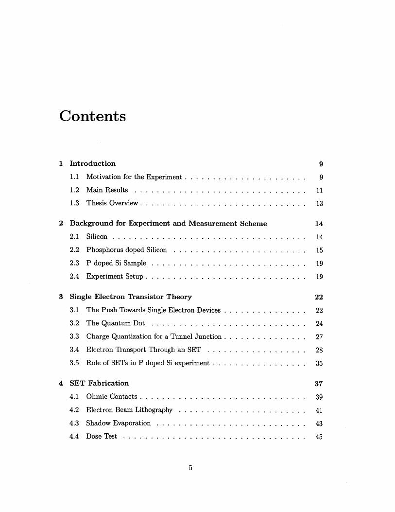
1 Introduction
1.1 Motivation for the Experiment . . . . . . . . . . . . . . . . . . . . . .
1.2 M ain Results . . . . . . . . . . . . . . . . . . . . . . . . . . . . . . .
1.3 Thesis Overview. . . . . . . . . . . . . . . . . . . . . . . . . . . . . .
2 Background for Experiment and Measurement Scheme
2.1 Silicon . . . . . . . . . . . . . . . . . . . . . . . . . . . . . . .. . . ...
2.2 Phosphorus doped Silicon . . . . . . . . . . . . . . . . . . . . . . . .
2.3 P doped Si Sample . . . . . . . . . . . . . . . . . . . . . . . . . . . .
2.4 Experiment Setup . . . . . . . . . . . . . . . . . . . . . . . . . . . . .
3 Single Electron Transistor Theory
3.1 The Push Towards Single Electron Devices
3.2 The Quantum Dot . . . . . . . . . . . . . .
3.3 Charge Quantization for a Tunnel Junction .
3.4 Electron Transport Through an SET . . . .
3.5 Role of SETs in P doped Si experiment . . .
4 SET Fabrication
4.1 Ohmic Contacts . . . . . . . . . . . . . . . .
4.2 Electron Beam Lithography . . . . . . . . .
4.3 Shadow Evaporation . . . . . . . . . . . . .
4.4 Dose Test . . . . . . . . . . . . . . . . . . .
5
9
9
11
13
14
14
15
19
19
22
. . . . . . . . . . . . . 22
. . . . . . . . . . . . . 24
. . . . . . . . . . . . . 27
. . . . . . . . . . . . . 28
. . . . . . . . . . . . . 35
37
. . . 39
. . . 41
. . . 43
. . . 45
4.5 Resist Thickness and Angle Determination . . . . . . . . . . . . . . . 46
4.6 Focus and Alignment Problems . . . . . . . . . . . . . . . . . . . . . 49
4.7 Successful SETs . . . . . . . . . . . . . . . . . . . . . . . . . . . . . . 50
5 SET Characterization 53
5.1 Preliminary Measurements . . . . . . . . . . . . . . . . . . . . . . . . 53
5.2 Measurement of Coulomb Blockade in SETs . . . . . . . . . . . . . . 54
5.3 Charge Sensitivity of SETs . . . . . . . . . . . . . . . . . . . . . . . . 57
5.4 Future Testing. . . . . . . . . . . . . . . . . . . . . . . . . . . . . . . 61
6 Conclusion 62
A SET Fabrication Recipes 64
A.1 Photolithography of Optical Gates . . . . . . . . . . . . . . . . . . . 64
A.2 Ebeam Lithography . . . . . . . . . . . . . . . . . . . . . . . . . . . . 65
6

List of Figures
1-1 Main Result: Coulomb Diamond Data for SETs .......
Cubic Structure of Silicon ......................
Band Structure of Silicon . . . . . . . . . . . . . . . . . . . . . . .
Transition between donor and donor-bound exciton states . . . . .
Spectrum of phosphorus-bound-exciton transitions . . . . . . . . .
Experiment Setup . . . . . . . . . . . . . . . . . . . . . . . . . . .
Circuit diagram of a single electron transistor . . . . . . . . . . .
Schematic of tunneling of an electron through an SET . . . . . . .
Energy parabolas for an SET . . . . . . . . . . . . . . . . . . . .
Schematic illustrating Coulomb blockade . . . . . . . . . . . . . .
Schematic representation of conductance through a quantum dot .
Schematic representation of current flow through an SET . . . . .
Schematic of Coulomb blockade diamonds . . . . . . . . . . . . .
2-1
2-2
2-3
2-4
2-5
3-1
3-2
3-3
3-4
3-5
3-6
3-7
4-1
4-2
4-3
4-4
4-5
4-6
4-7
4-8
7
. . . . . 12
15
16
18
19
21
23
. . 29
30
. . 31
33
35
. . 36
Schematic of an SET . . . . . . . . . . . . .
Image of file used in SET fabrication . . . .
Schematic of photolithography procedure .
Image of file used to specify SET features .
Schematic of SET angle evaporation . . . . .
Determination of critical evaporation angle .
SEM image of dose test pattern . . . . . . .
SEM image of dose test results . . . . . . . .
. . . . . . . . . . . . 38
. . . . . . . . . . . . 38
. . . . . . . . . . . . 40
. . . . . . . . . . . . 42
. . . . . . . . . . . . 44
. . . . . . . . . . . . 45
. . . . . . . . . . . . 46
. . . . . . . . . . . . 4 7

4-9
4-10
4-11
4-12
4-13
4-14
4-15
5-1
5-2
5-3
. . . . 48
. . . . 49
. . . . 49
. . . . 50
. . . . 51
. . . . 51
. . . . 52
SET evaporation at less than critical angle . . . . . . . . . . .
SEM image of mesa with unsuccessful liftoff . . . . . . . . . .
SEM image of a broken SET island . . . . . . . . . . . . . . .
SEM image of SET alignment to ohmic contacts . . . . . . . .
SEM image of successful SETs with narrow features . . . . . .
SEM image of successful SETs but with bad ohmic contacts
SEM image of successful sample tested in dilution refrigerator
Measurement of Coulomb blockade diamonds . . . . . . . . . .
Measurement 1 for charge sensitivity determination . . . . . .
Measurement 2 for charge sensitivity determination . . . . . .
8
56
58
60

Chapter 1
Introduction
1.1 Motivation for the Experiment
Quantum information offers new paradigms with the promise to revolutionize comput-
ing and cryptography. This vision can only be realized with the ability to coherently
control and manipulate quantum systems. While a classical bit can be either 0 or
1, quantum bits (qubits) can exist in a superposition of these classical states simul-
taneously. The potential for feasible qubits was first seen in atomic physics, where
the internal levels of atoms and ions present a natural set of quantum states. These
states are isolated using laser cooling and cavity modes and manipulated using op-
tical transitions. Solid-state systems are now emerging as promising candidates for
electron and nuclear spin-based qubits. The ideas developed in the context of atomic
systems can be readily applied in the solid state, which offer additional advantages in
terms of modern fabrication techniques, scalability, tunability and integration with
existing technology.
The primary challenge of using spins as qubits lies in the detection of a single spin.
Most single qubit measurement schemes use either optical or electrical methods for
both initialization and readout. However, due to low detection efficiencies and noisy
backgrounds, these methods have severe bottlenecks. We plan to investigate a novel
hybrid technique that combines the advantages of spin selective optical excitations
with that of electrical readout measurements to detect spin defects in solid state sys-
9

tems. We focus on the measurement of individual electron spins of phosphorus-doped
silicon and ultimately hope to achieve single shot readout of the electron spin state
which means that once the spin is initialized, its readout occurs within a coherence
time.
Phosphorus-doped silicon is a prime candidate for spin based qubits for a variety
of reasons. Given its ubiquity in the semiconductor industry, Si samples are readily
available and fabrication techniques are well established. The weak spin orbit coupling
in silicon gives rise to long coherence times, an essential feature for information storage
in a qubit [22]. Additionally, P doped Si is an example of a solid state system with
a spin selective optical transition that can be exploited for initialization of the qubit.
A narrow linewidth laser is used to optically excite the P donor from the neutral
state to the excited donor-bound exciton state [4]. A specific spin state of the donor
can be isolated by using a small 1-2 Tesla magnetic field to Zeeman split the spin
degeneracy of the electrons. This gives us the ability to address a P valence electron
in a particular spin state by tuning the laser frequency appropriately.
The excited donor-bound-exciton state decays most often via the Auger process,
ionizing the donor, ejecting an electron and leaving behind a P+ ion [19]. One could
choose to optically readout the ejected electron. However, this would result in a rather
weak emission signal from a single donor over a broad frequency range, making single
shot readout impractical. We therefore turn to using electrical detection methods to
see whether the P atom was ionized or not. We do so using single electron transistors
(SETs).
An SET is a nonlinear, nano-electronic device consisting of two tunnel junctions,
a source and a drain, capacitively coupled to a small island of electrons [12]. This
device is capable of highly sensitive measurements of the local charge. In the regime
where the energy levels of the source and the drain are below the potential of the
island, electron tunneling from source to drain is forbidden. However, the presence
of the P+ ion shifts the potential of the island [19]. This results in a sharp peak in
the current through the SET that can be used for single shot readout and thus for a
measurement of the spin state of the electron [5].
10

The presence of a nuclear spin of the P atom, in addition to the spin of the elec-
tron, gives rise to the possibility of exploiting the hyperfine splitting for information
storage. The considerably longer coherence times of the P nucleus opens the door
for exploring entanglement of multiple qubits, essential for harnessing the power of
quantum information processing, and the possibility of scalable quantum computers
[11]. Another novel application of this system is in the realm of high precision magne-
tometry to measure very small magnetic fields measured through modulations of local
Zeenman shifts [19]. Additionally, this hybrid technique of optical initialization and
electrical readout is very versatile and can be extended to other solid state systems
such as nitrogen vacancy centers in diamond.
1.2 Main Results
My senior thesis project involved designing and fabricating singe electron transistors
(SETs) for electrical readout of the spin state of the P donor in Si. The ability to
use an SET for a highly sensitive measurement requires the characteristic charging
energy, Ec, of the SETs to be much larger than the thermal energy of the charge
carriers. Therefore the experiment will be conducted in a cryostat which is capable of
consistently reaching a stable temperature of ~ 1.5K. Thus my ultimate goal was to
fabricate SETs on P doped Si samples that function at temperatures of about 2K. This
necessitated minimizing the tunnel junction area through optimized lithography and
evaporation procedures in order to decrease the capacitance and therefore increase the
charging energy. These SETs were tested in a dilution refrigerator at a temperature
of 10mK. We see very nice Coulomb oscillations and Coulomb blockade diamonds as
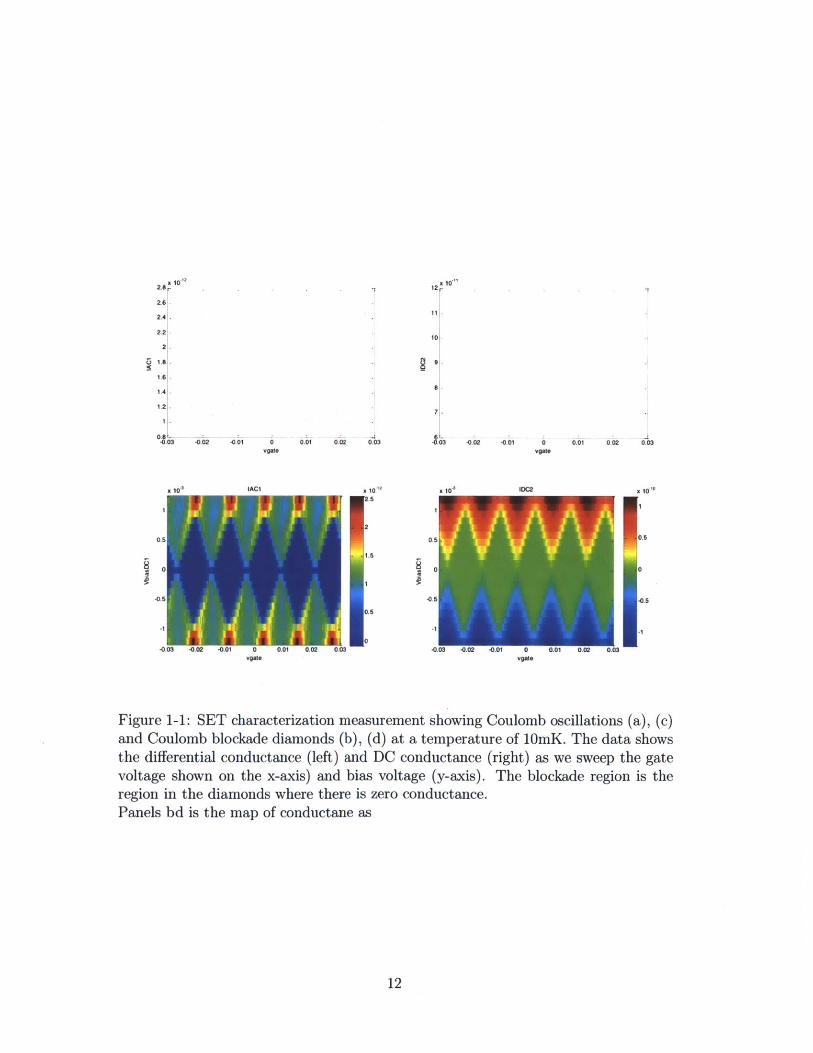
we sweep the bias and gate voltages as shown in Fig. 1-1. Each oscillation is indicative
of a single electron tunneling onto the island. I have successfully produced SETs with
charging energies of ~ 0.85 meV corresponding to a temperature of ~ 10 K. These
SETs have a charge sensitivity of 2 x 10- e//fiz at 10 mK. They will be tested at
temperatures of 2K once our cryostat arrives.
11
12r
101
9
12
0.02 0.03 083
x 10
2
1.5
10.5
0
-0.02 -001 0vgate
2
0.01 002 0.03
x 10",
I
05
0
40.
V98At
Figure 1-1: SET characterization measurement showing Coulomb oscillations (a), (c)and Coulomb blockade diamonds (b), (d) at a temperature of 10mK. The data showsthe differential conductance (left) and DC conductance (right) as we sweep the gatevoltage shown on the x-axis) and bias voltage (y-axis). The blockade region is theregion in the diamonds where there is zero conductance.Panels bd is the map of conductane as
12
226 10
2.41
2.21
2
S1.6
1.6
1.23
1~6
-0.02 .001 0vgate
0.01
Vgate
Uri
1.3 Thesis Overview
This thesis is organized as follows. Chapter 2 contains some of the theory behind the
experiment, background information on the experimental setup as well as the expected
measurement scheme. In Chapter 3 of this thesis, I present the theory of electron
transport through a single electron transistor and discuss how it can be used for very
sensitive charge detection. In Chapter 4, I describe the fabrication procedures that I
developed for producing SETs. Chapter 5 shows measurements made to characterize
the operating temperature and sensitivity of these SETs. Finally, in Chapter 6,
I summarize the results of my experiment and discuss the future directions of the
experiment.
13
Chapter 2
Background for Experiment and
Measurement Scheme
In our experiment, we plan to investigate a novel hybrid technique that combines the
advantages of spin selective optical excitations with that of electrical readout mea-
surements to detect spin defects in solid state systems. The measurements focus on
individual electron spins of phosphorus-doped silicon and ultimately hope to achieve
single shot readout of the electron spin state which means that once the spin is ini-
tialized, its readout occurs within a coherence time. In this chapter, I discuss the
theory needed to understand the general setup of our experiment and then move on
to describing the proposed experimental setup. I start with a little bit of background
on silicon. I then describe phosphorus doped silicon, and its spin selective optical
transition. Next I briefly discuss the P doped Si samples used in the experiment.
Finally, I sketch the setup used to measure the spin state of the electron and briefly
talk about the measurement scheme.
2.1 Silicon
Silicon (Si) has a diamond crystal structure which can be described by a face-centered
cubic lattice with two atoms per unit cell. The basis consists of two atoms located
at (0,0,0) and (i, i, (), with the lattice constant for silicon, a being 5.43 A. The
14

Figure 2-1: A unit cell of the face-centered cubic lattice for silicon. Taken from [21].
structure is shown in Fig. 2-1 where each atom sits at the center of a tetrahedron
built from its four nearest neighbors.
The band structure of silicon is shown in Fig. 2-2 (a). Silicon has an indirect band
gap, where the minimum of the conduction band occurs at k = 0.85(27r/a)(1, 0, 0) [8].
Thus there are six symmetry-related equivalent minima in the Brillouin zone. These
constant-energy surfaces near the conduction band minima are ellipsoidal pockets
with the long axes directed along the (100) directions shown in Fig. 2-2 (b) [1]. The
valence band minimum occurs at k = 0 where the degenerate "light hole" and "heavy
hole" bands with different effective masses meet.
2.2 Phosphorus doped Silicon
The phosphorus (P) substitutional dopant in Si supplies additional electrons to the
conduction band, which act as donors. When a P atom with electronic configuration
(3S2 3p3) substitutes for Si atom (3s2 p2) it acts as an additional positive charge
with an extra electron bound to it and can effectively be modeled as a hydrogen-like
atom embedded in the Si lattice. To first approximation, if we ignore the difference
in structure between the phosphorus and silicon ion cores, the phosphorus can be
considered as an additional positive charge placed on a Si site, along with an additional
15
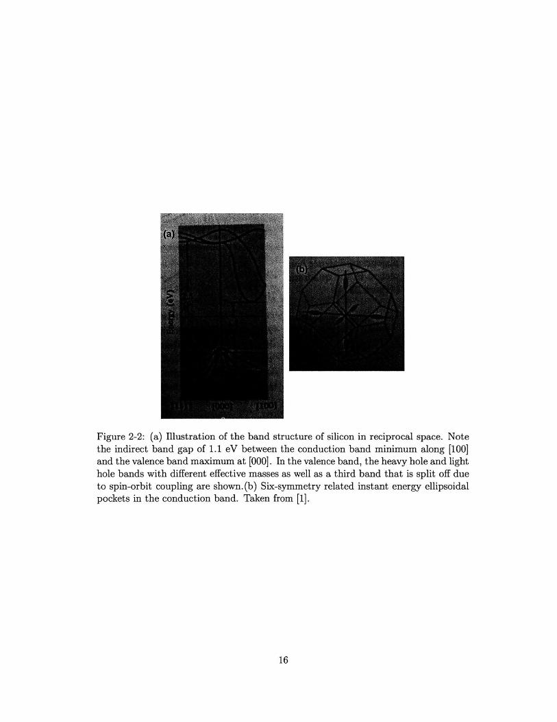
Figure 2-2: (a) Illustration of the band structure of silicon in reciprocal space. Notethe indirect band gap of 1.1 eV between the conduction band minimum along [100]and the valence band maximum at [000]. In the valence band, the heavy hole and lighthole bands with different effective masses as well as a third band that is split off dueto spin-orbit coupling are shown.(b) Six-symmetry related instant energy ellipsoidalpockets in the conduction band. Taken from [1].
16

electron. This gives rise to a screened Coulomb potential between the the extra donor
electron and the P nucleus.
We estimate the binding energy of the donor electron around the P+ ion to be
m* 1Eb = - x 13.6 eV, (2.1)
me (e/co)2
where me is the mass of the electron, m* is the effective mass, co is the permittivity
of free space and E is the dielectric constant. The radius of the bound state is ro =
(m/m*)( c/eo) ao, where ao = 0.53 A is the Bohr radius of the Hydrogen atom. Using
m* = 0.3m and E = 12co for Si gives a binding energy Eb = 45meV ~ 52K [1]. These
corrections lead to a binding energy of the donor electron that is greatly reduced
compared to that of a hydrogen atom. Thus the electron donor is loosely bound to
the P atom can be ionized into the conduction band depending on the temperature
[1].
Typically, in semiconductors, a photon with energy above the band gap excites an
electron from the valence band to the conduction band, leaving behind a hole in the
valence band. An exciton is a negatively charged electron bound by the Coulomb
interaction to a positively charged hole. The lifetime of an exciton ranges from
nanoseconds to milliseconds after which the electron and hole recombine to emit a
photon of characteristic energy. In indirect band gap semiconductors such as silicon,
this process is assisted by a wave vector conserving phonon [1].
Phosphorus doped Silicon is an example of a solid state systems with a spin selec-
tive optical transition between the neutral P donor state to the donor-bound-exciton
state. The ground state of the P neutral donor state, Do, consists of the positive P
donor ion bound to the donor electron. The donor-bound-exciton DOX consists of
two interacting electrons and one hole, as well as the fixed positive donor ion. It is
energetically favorable for these two electrons to form a spin-singlet. Since the ab-
sorption of a photon gives rise to the donor-bound-exciton state, in order to conserve
momentum, the hole has Jh = 3/2 making its wave function four fold degenerate. A
schematic is shown in Fig. 2-3.
17
(a) (b) 44I +
Figure 2-3: (a) Optical transition between the donor (DI) and the donor-bound-exciton (D0X) states. The electrons form a singlet. (b) The Zeeman splitting of thestates in the presence of a magnetic field. Taken from [19].
In this system, the Auger process dominates the relaxation, where energy resulting
from the recombination of the electron hole pair is used to ionize the donor, leaving
behind an ionized P+ and an energetic free electron [19].
A weak magnetic field of 1-2 Tesla is applied to the sample in order to Zeeman
split both the ground and excited states. The applied field lifts the donor electron
spin degeneracy of the D' ground state, splitting it into two levels determined by the
projection of the electron spin. Technically, the hyperfine interaction between the
electron and nuclear spins can also be resolved. The current experiment is focused
on the spin of the electron but can be extended in the future to take the hyperfine
interaction into account. The D0X state has two electrons in a spin singlet state.
Thus, in the presence of a magnetic field, the Jh = 3/2 spin of the hole determines
the level splitting, splitting into four Zeeman levels [4]. The Zeeman spectrum of the
phosphorus bound exciton transitions is shown in Fig. 2-4.
18

(a)
I14989
Figure 2-4: (a) Spectrum of phosphorus-bound-exciton transitions in isotopically pu-rified Silicon. The six doublet transitions allowed by selection rules are shown in (b).They are ordered in increasing energy from left to right in correspondence with theones shown in (a). Taken from [4].
2.3 P doped Si Sample
We use single electron transistors (SETs) to detect whether a P atom was ionized
via the Auger process. We pattern these SETs directly onto the P doped Si sample.
Ideally we would like to have the SETs as close to the P dopants as possible. We
ordered neutron transmutation doped (NTD) Si wafers from Silicon Quest Interna-
tional. These wafers offer an advantage in terms of better spatial distribution of the
dopants. The NTD process involves irradiating neutrons into an undoped, highly
purified silicon sample. Through radioactive decay a Si atom transmutes into a 31p
atom. The sample has a 500 Ohm-cm resistivity with 8 x 10¹² P atoms / cm 3 Si with
a spacing of 500 nm/P atom. The 4 inch wafer is 375 pm thick with a single side
polished. Preliminary testing of SETs was done on ordinary P doped Si samples with
resistivities of 1-10 Ohm-cm.
2.4 Experiment Setup
As discussed in the introduction, the ultimate goal of this experiment is to implement
a hybrid optical initialization with electrical readout scheme. The plan for the setup
19

of our experiment looks something like Fig. 2-5. The experiment is in the early
stages of being set up. The first step involves fabricating SETs on the P doped Si
sample. After fabrication, the sample will be placed in a cryostat in order to cool
the sample and achieve temperatures below the charging energy of the SET. The
cryostat is a pumped helium (4K) system with a 2T magnet. In the dynamic flow
regime, the temperature can consistently remain stable at ~ 1.5K. This temperature
is the limiting factor for our SET charging energy. The cryostat has been ordered
and is to arrive soon (by the end of May 2012).
The sample is then optically excited using a near infrared 1078nm Yb-doped Fiber
laser. We thermo-piezo-electrically tune the laser to one of the specific transition
shown in Fig. 2-4. A wave meter is used to precisely monitor the frequency of the
laser. The laser is mechanically chopped in order to allow for the elimination of noise
from all sources except the donor-bound-exciton decay. This blocking and unblocking
of the laser gives us the ability to perform an AC measurement of the effects of the
excitation laser on the P donors of the sample. The electron only gets excited if it
is in the spin state with the same frequency as the laser frequency to which we have
tuned. If the two frequencies are the same, the donor (P+ + e-) will be excited, form
a donor-bound-exciton (P+ + e- + e- + h+), and then decay via the Auger process.
We ultimately wish to detect the spin state of the electron, i.e. whether the laser
frequency was able to excite the donor. This is done by using the SET to electrically
detect the charge of the the P, i.e. whether the P donor was ionized via the Auger
process or not.
20

Figure 2-5: Schematic diagram showing the setup of the experiment. The P doped Sisample with fabricated SETs is placed in a helium cryostat. The donors are opticallyexcited using a narrow linewidth laser which can be tuned to a desired frequency.The SETs are then used to detect whether the donor was ionized.
21

Chapter 3
Single Electron Transistor Theory
This chapter presents the details of electron transport through a single electron tran-
sistor (SET) by examining the roles played by each of the different components of an
SET. I start with the motivation for the push towards exploiting quantum mechanical
properties in a transistor. Next, I discuss how the island of an SET functions like a
quantum dot and then discuss the properties of a single tunnel junction. I then put
all these components together and explain transport though an SET and the depen-
dence of current flow on the bias and gate voltages. Finally, I describe how the SETs
are used in the experiment to detect the charge of the phosphorus donor.
3.1 The Push Towards Single Electron Devices
The semiconductor transistor has been a very remarkable invention which is now an
indispensable component of all modem electronics. Since its invention in the 1940's,
the trend toward miniaturization of transistors has been very rapid, opening endless
opportunities in the realm of information acquisition, processing, data storage and
communication technologies [2]. As devices get smaller, faster and more densely
packed, quantum effects become increasingly important for device operation. An
example of such a device is the single-electron transistor (SET) which will be explored
in great detail in the rest of this chapter. Electron transport in an SET is governed
by the tunneling of electrons through an insulating barrier, a feat that cannot be
22
(a) (b) c CD
source dot drain
souvse
plunger
Figure 3-1: (a) Schematic of a single electron transistor. Taken from [10]. (b) illus-trates the capacitance model for the SET.
explained classically.
The fabrication of tunnel junctions with increasingly smaller dimensions has made
it possible to observe the quantum mechanical tunneling of a single electron through
an insulating barrier. The SET consists of two tunnel junctions placed in series,
forming an island between them. This island is a region containing localized electrons
which functions like a quantum dot. It is coupled to a source and drain contact via
tunnel junctions. The source and drain terminals connect the island to macroscopic
current and voltage meters. We describe the SET using a circuit diagram as shown
in Fig. 3-1. The functioning of an SET is governed by a combination of the quantum
phenomenon of tunneling of an electron through a metal-insulator-metal junction and
the Coulomb interactions on the island.
Fulton and Dolan were the first to demonstrate successful SETs in 1987 [7]. Since
then SETs have been realized using a variety of fabrication methods and materials,
including metallic, semiconducting, molecular and nanotube based devices. These
different incarnations of the SET allow for different operational schemes and temper-
atures [20]. Typically, metallic based devices are operated in the milli-Kelvin temper-
ature range, though there have also been devices that operate at room temperature
[16, 17]. The operating temperature is an important parameter, as it partially de-
fines the energy conditions which dictate electron tunneling events through the SET.
23

Current efforts have been focused on raising the operating temperature of the de-
vice in the hopes of overcoming one of the main drawbacks in the implementation of
single-electron devices.
The most outstanding property of SETs is the possibility to switch the device from
the insulating to the conducting state by adding only one electron to the gate elec-
trode, whereas a common MOSFET needs about 1000 to 10,000 electrons [19]. This
reduction in the number of electrons in a switching transition greatly reduces circuit
power dissipation, raising the possibility of even higher levels of circuit integration
[4].
SETs are extremely versatile in their applications. They can be used as very
precise temperature sensors, magnetometers and electrometers [18]. They are already
outperforming state-of-the-art conventional transistors by three orders of magnitude.
Their charge sensitivity has been shown to be as low as a few 10-5e/Vilz, which
means that a charge variation of 10-e can be detected in a measurement time of is
where the precision improves as the square root of the measurement time [2].
3.2 The Quantum Dot
The SET consists of an island that connects a source and a drain via two tunnel
junctions. This island is a quantum dot, with the defining feature that it contains
localized electrons. In the past couple of decades, various structures have been fab-
ricated to confine electrons to small volumes in both semiconductors and metals. A
system of confined electrons will have discrete charge and electronic states . They
are often called artificial atoms or quantum dots in order to reflect the importance
of quantization phenomena on their properties [15, 14]. I now discuss the similarities
and differences between the semiconductor and metallic quantum dots which can be
seen in two limiting cases: (1) the case with a few electrons on the dot where the
discrete level spacing is comparable to the charging energy and (2) the case with
many electrons on the dot where the level spacing is much smaller than the charging
energy [20]. I make some estimates of the energy scales involved using simple models
24
in order to get a feel for the physics.
Semiconducting Dots:
In semiconductors, electrons fill only a few levels of the conduction band. At the
nanometer length scale, quantum dot devices have been fabricated where the electrons
occupy discrete energy levels. These devices function like "artificial atoms," where
the discrete excitation spectrum is analogous to atomic orbitals in atoms [13]. In
these devices, the confinement of the electron can be modeled by a single particle in a
box. This discreteness of levels is important because the level spacing is comparable
to the chemical potential. The characteristic energy level spacing for a dot of typical
radius R is given by:
5E - -*-r (3.1)2me, R2 mn*'
where me is the rest mass of the electron and m* is the effective mass of the electron
in the system [20].
We estimate the energy level spacing for a dot of size R = 100nm. In a semi-
conductor, the effective mass of an electron is approximately m* ; 0.1me, giving
an estimate of the energy level spacing to be 6E = 0.4meV ~ 4K. The number of
electrons in a semiconducting dot is determined primarily by the dopant density that
fill only the low lying states.
Metallic Dot:
Most metallic dots contain a large number of electrons, so Eq. 3.1 cannot be used
to describe the energy spacing of the levels. The average level spacing at the Fermi
energy is quite small and should be estimated using a density of states argument [14].
In our SETs, the island has dimensions much larger than the the lattice spacing of
aluminum. Thus, we can approximate the number density of the dot as that of bulk
aluminum. Assuming a 3 dimensional spherical dot, for a density n = 18 x 10 22/cm 3 ,
the number of electrons on the dot is on the order of N = 4/37rR3 x n ; 10 9 [1].
Given the number of electrons, the picture is different from the semiconductor dot
picture. With so many levels of the dot filled, we are no longer probing the bottom
levels of a band. We can therefore view the metallic dot as a collection of a large
25

number of electrons filling up states up to the Fermi level EF. From this description,
we estimate the energy level spacing (up to constant factors arising from geometry)
from the inverse density of states g(eF) since 6E = 1/g(eF), where the density of
states is the number of states per energy [14]. Given that EF = h 2 / (2m) and
k' = 37r2 N/V we obtain g(eF) = dN/deF = 3N/(2eF). For a 3-D, 100nm Al dot
with a Fermi energy 6F = 10eV this gives a level spacing of about 0.6 x 10- 5 meV
which is much smaller than the estimate of a particle in a box. Thus we see that
in a metallic quantum dot, the discrete energy spacings are very close together and
cannot be resolved in most measurements.
Role of Coulomb Interactions in Quantum Dots:
If a quantum dot is relatively isolated electrically from its environment, it has
a set of well defined charge states. Each successive charge state corresponds to an
addition of one more electron to the dot. The charging energy Ec of a quantum dot is
similar to the ionization energy of an atom, defined to be the energy required to add
or remove a single electron to the dot. Because of the Coulomb repulsion between
electrons, the energy between successive charge states can be very large.
The primary difference between metallic and semiconducting dots is that in the
metallic dots the charging energy is much much larger than the level spacing whereas
in the semiconducting dots they are comparable. In a metallic dot, given the large
number of electrons, the level spacing is given by the inverse density of states. In
semiconducting quantum dots, the energy level spacing can be modeled by the con-
finement of a few electrons in a box. However, what is important for the functioning
of the SET is the possibility to measure charge quantization using either metal or
semiconducting dots. Both types of dots share the fact that the Coulomb energy is
an important energy scale and determines the quantum transport through the dot.
The SETs fabricated for this experiment are made of aluminum, consisting of
islands with dimensions approximately 50nm by 50nm by 500nm and are best under-
stood by the metallic quantum dot description.
It is also interesting to contrast the behavior of metallic dots vs. bulk metals. In
the bulk of a metal, the electronic states are extended plane wave states resulting in
26

bands. The Coulomb interaction evaluated using these plane wave states are typically
much smaller than the band width electron correlations can be neglected in bulk
metals. Therefore it is possible to add an electron right at the Fermi energy EF (at
low temperatures) in the bulk metal. As electronic wave functions get localized on
the quantum dots, the Coulomb interactions between these localized wave functions
become significant. As a result the energy to add an extra electron on the metal dot
becomes EF + Ec, where Ec is the charging energy discussed above.
3.3 Charge Quantization for a Tunnel Junction
For a tunnel junction, i.e. two metallic electrodes separated by an insulating barrier,
an electron at the Fermi energy of one of the electrodes can pass through the barrier to
the other electrode, even though classically, the electron energy is too low to overcome
this barrier. The charge Q transferred through the barrier is quantized by amount e,
so the charge on the island is given by Q = Ne, where N is an integer. The number
of electrons N is such that the energy of the entire circuit is minimized.
When a tunneling event occurs, the charge on the island changes by the quantized
amount e. The associated change in the electrostatic potential of the island is Ecle
where the charging energy, Ec = e2/2Cj is expressed in terms of the capacitance of
the junction Cj. In order for the thermal energy to not mask the Coulomb effects,
we require that charging energy exceeds the temperature,
> kBT. (3.2)2Cj
This condition can be met by having tunnel junctions with a small capacitance which
translates to having a small junction size, since for a parallel plate capacitor, C =
cA/d.
Adding an additional electron to the island takes a time At = RtCj given by
the RC-time constant of the island. In order to resolve the charging energy AEc =
e2 /2Cj, we must impose the condition that the system obeys the Heisenberg uncer-
27
tainty relation AEAt > h/2. Thus the tunneling resistance Rt of the quantum dot
has to be larger than the quantum resistance,
hRt >> h. (3.3)
This criterion can be met by weakly coupling the island to the source and drain leads
[10].
As an example, let us note that a junction with an area of about 0.1 x 0.1Im 2 and
a typical oxide layer thickness of 10A has a capacitance of about 10-F corresponding
to a temperature of about 1K. For decreasing capacitance, which requires decreasing
dimensions of the junction, this restriction for temperature becomes more relaxed.
3.4 Electron Transport Through an SET
Recall that an SET consists of an island coupled via tunnel junctions to a source and
a drain and capacitively coupled to a gate. See Fig.. 3-1. Current flows through an
SET when an individual electron tunnels through one of the tunnel junctions onto
the island and then from the island through the other tunnel junction. A schematic
of single electron tunneling is shown in Fig. 3-2. Thus the charge on the island is
quantized and can only change in discrete units of e. When current flows through the
SET, the charge on the island oscillates between N and N + 1 electrons.
The energy of the island with N electrons on it is given by
Ed (N, Vg, VSD) = (-en + Qo) 2
2Cs 34
with Cr being the total capacitance given by CE = Cs + CD + Cg and n = N - No
where N is the number of electrons on the island and No is the number of electrons
at zero gate voltage and zero bias voltage. The continuous part of the excess charge,
induced by the gate and bias voltages is given by
Qo = CsVs + CDVD + CgVg. (3.5)
28

(a) (b)
Figure 3-2: Schematic depicting how the tunneling of an individual electron throughthe source and drain tunnel junctions via the island induces a current flow through theSET. (a) shows the situation with N electrons on the dot and (b) shows the situationwith N + 1 electrons on the dot. An additional electron on the island increases itsenergy by Ec = e2/2CE or the potential by Ec/e. When current flows through theSET, the charge on the island oscillates between N and N + 1 electrons. (a) and (b)show the sequential tunneling process at the same gate voltage. Modified from [20].
29

Figure 3-3: Energy parabolas showing the interplay between the continuous anddiscrete charges on the dot.Taken from [201.
For each value of n, the number of electrons on the dot, we get an energy parabola,
plotted in Fig. 3-3. With a gate voltage it is possible to change the number of electrons
on the dot. For a fixed value of Qo there is a minimum energy cost for the dot to change
the electron number. While the tunneling of a single charge changes the electrostatic
energy of the island by a discrete value, a voltage V applied to the gate can change
energy of an island in a continuous manner. At Qo/e = i1/2 integer values two
different charge states with different numbers of electrons become degenerate. At
these values of the gate voltage, charges leads to conductance dI/dV oscillations as
a function of gate voltage, also known as Coulomb oscillations.
The energy required to add an additional electron to the island is known as the
charging energy. The charging energy is given by
Ec = . (3.6)2CE'
To be able to resolve the charging energy of an SET is very similar to that of an
individual tunnel junction, and is given by
Ec = - > kBT. (3.7)2Cs
In this case C is the total capacitive coupling to the environment, which for an SET
is given in terms of the source, drain and gate capacitances: Cr = Cs + CD ± C g-
30
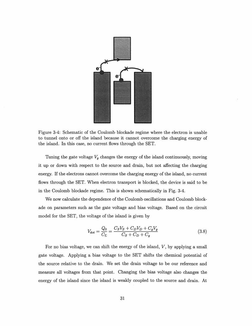
Figure 3-4: Schematic of the Coulomb blockade regime where the electron is unableto tunnel onto or off the island because it cannot overcome the charging energy ofthe island. In this case, no current flows through the SET.
Tuning the gate voltage Vg changes the energy of the island continuously, moving
it up or down with respect to the source and drain, but not affecting the charging
energy. If the electrons cannot overcome the charging energy of the island, no current
flows through the SET. When electron transport is blocked, the device is said to be
in the Coulomb blockade regime. This is shown schematically in Fig. 3-4.
We now calculate the dependence of the Coulomb oscillations and Coulomb block-
ade on parameters such as the gate voltage and bias voltage. Based on the circuit
model for the SET, the voltage of the island is given by
Vdot - Qo _ CSVS + CDVD + CgVg (3.8)CE CS+CD+Cg
For no bias voltage, we can shift the energy of the island, V, by applying a small
gate voltage. Applying a bias voltage to the SET shifts the chemical potential of
the source relative to the drain. We set the drain voltage to be our reference and
measure all voltages from that point. Changing the bias voltage also changes the
energy of the island since the island is weakly coupled to the source and drain. At
31

zero temperature, current flows through the SET when the number of available states
on the island in the energy between Vs and VD is non-zero.
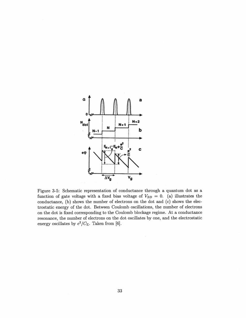
First, for zero bias voltage, as we sweep the gate voltage, the conductance oscillates
between zero (Coulomb blockade) and non-zero (no Coulomb blockade) as illustrated
in Fig. 3-5. In the case of zero conductance, the number of electrons N on the island
is fixed. At the conductance maximum, this number oscillates between N and N +1.
We now derive the period of oscillations in gate voltage corresponding to conducting
resonances through the SET. The energy of an island with N electrons is given by
Edt(N) = (-en ± Qo) 2 (3.9)2CE
Therefore, the energy difference between an island with N + 1 electrons versus N
electrons is given by
Edot(N + 1) - Edt(N) = (n - 1/2) e- - Q (3.10)Cr, CE,
For zero bias voltage, Vs = VD = 0,
e2 C VgEdot(N + 1) - Edt(N) = (n - 1/2) - e . (3.11)
Cr, CE
As we saw in Fig. 3-3, At the intersection points of the E(N) and E(N+ 1) parabolas,
we get a conductance peak through the SET. In order to find the gate voltage when
E(N + 1) = E(N), we set Eq. 3.11 to zero, giving:
14(n) - (n - 1/2)e (3.12)Cg
Thus, for zero bias voltage, in order to find the period of oscillations in gate voltage,
AV, corresponding to a change of one electron, is given by
AV = V(n + 1) - V(n) = . (3.13)A9
A 2D plot of the conductance as the bias voltage and gate voltage are swept
32
AVO Vg
Figure 3-5: Schematic representation of conductance through a quantum dot as afunction of gate voltage with a fixed bias voltage of VSD = 0- (a) illustrates theconductance, (b) shows the number of electrons on the dot and (c) shows the elec-trostatic energy of the dot. Between Coulomb oscillations, the number of electronson the dot is fixed corresponding to the Coulomb blockage regime. At a conductanceresonance, the number of electrons on the dot oscillates by one, and the electrostaticenergy oscillates by e2/CE . Taken from [6].
33

shows the characteristic Coulomb diamonds a schematic of which can be seen in in
Fig. 3-7. The height of the diamond is proportional to the charging energy and given
by 2 * e/2C, and the width is given by AV = e/Cg. As per the chemical potential
picture shown in Fig. 3-6, the slopes of the Coulomb diamond are defined by VD = Vot
and Vs = Vot. From these equations it is possible to derive the explicit relationship
between the bias voltage and the gate voltage in terms of the various capacitances in
the system.
In order to determine the slopes of the Coulomb diamonds, i.e. the regions of
current flow, we apply a fixed positive gate voltage V to the SET, and adjust the
bias voltage such the energies of the source or drain is equal to the energy of the
island.
For a forward biased SET, current will flow when Vs = Vot as shown in Fig. 3-6
(a). This condition gives rise to the equation
= CSVS +CDVD + CgVg (3.14)
Setting VD = 0 and solving for Vs/IV, we get
V- = = (3.15)6g CE-Cs C,+CD(
For a reversed biased SET, we want the condition, VD= Vo as shown in Fig. 3-6
(b). Since VD is our reference, we have
CsVs+CDVD+C9 g0 = . (3.16)
Solving for Vs/V, we getVs C9 (3.17)V9 Cs.
Thus Eq. 3.15 and Eq. 3.17 give us the slopes of the Coulomb diamonds. We see
that Eq. 3.15 and Eq. 3.17 are not symmetric under the exchange of Cs and CD. This
is due to the fact that the we set the drain as the reference and apply the bias voltage
34

(a) (b)
Vs Vdot
VD=O Vdot
Vs
VS.ss
-VSD
Figure 3-6: Schematic representation of energy of island compared to that of the
source and drain during current flow through an SET. For a positive gate voltage, (a)
shows the onset of current flow for a forward biased SET and (b) shows the onset of
current flow for a reverse biased SET.
solely to the source. We perform the calculation for this case because in our transport
experiments, we ground the drain and apply a bias voltage to the source. If we were
to apply half of the bias voltage to the source and half to the drain, then the slopes
of the Coulomb diamonds would be equal and opposite. However, the capacitances
measured from the slopes should be the same, regardless of how the bias voltage is
divided between the source and the drain.
3.5 Role of SETs in P doped Si experiment
For the experiment, we make the island and the source and drain leads of the SET
from Aluminum. The SETs are fabricated directly on the P doped Si sample. This
sample is placed in a cryostat in order to satisfy the condition that the charging energy
of the SET is much greater than the temperature. The sample is irradiated with laser
light tuned to a specific frequency. We then use the SET to electrically detect the
35

Vsg
N electronson island Vgate
9
Figure 3-7: Schematic of the Coulomb blockade diamonds. Current flows in the graytriangular shaped regions. The white regions correspond to a gap in current flow witha fixed number of electrons on the island. Modified from [10].
charge of the P donor. If the P is ionized via the Auger process, the presence of the
P+ ion will shift the electrochemical potential of the island, with its effects similar to
that of applying a gate voltage to the SET. From the above discussion, we see that
this results in a sharp peak in the current through the SET, which can ultimately
be used for single shot readout and thus for a measurement of the spin state of the
electron. The next chapter of this thesis discusses the details of the fabrication of
these SETs, and the following chapter presents measurements of the charging energy
and charge sensitivity of the SETs that are to be used in the experiment.
36

Chapter 4
SET Fabrication
In this chapter, I discuss the fabrication procedures used to pattern SETs on a silicon
substrate. First, photolithography is used to pattern ohmic contacts onto our sample.
The gates allow us to make electrical contact between external voltage sources and
the leads of the SET. Two stages of photolithography are involved in order to ensure
good electrical contact at both ends. After the ohmic contacts are patterned on the
sample, we write the leads and island of the SET using electron beam lithography.
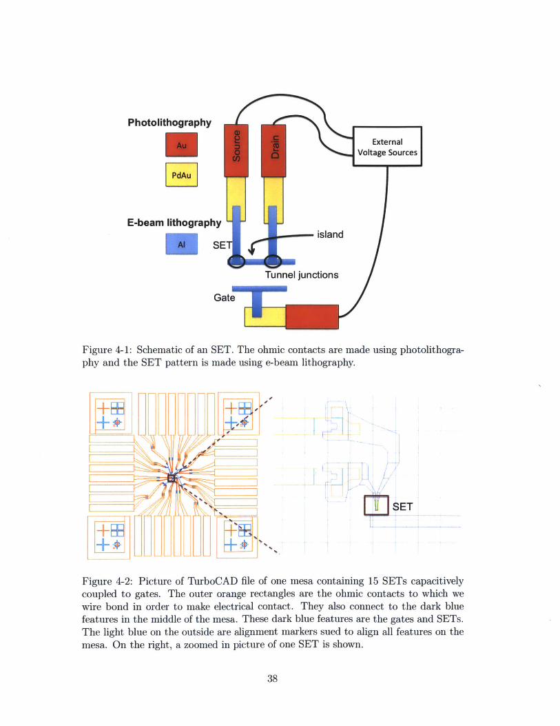
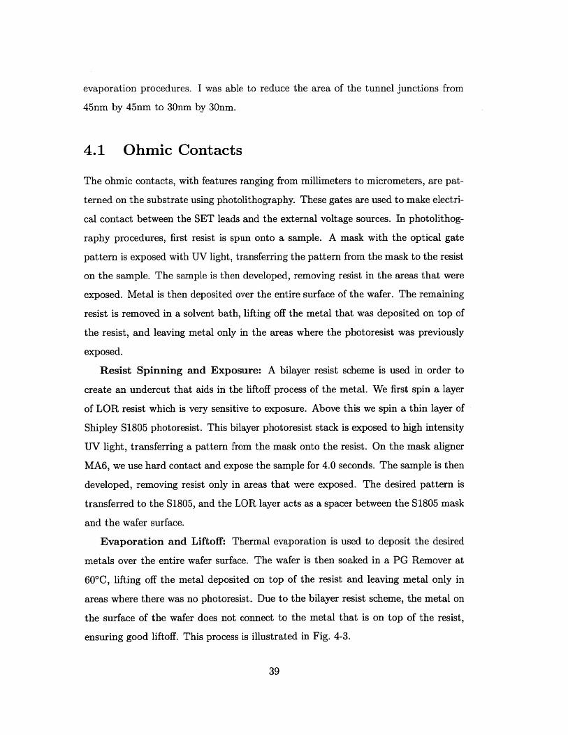
Fig. 4-1 is a schematic of the various features written during the entire fabrication
process for a single SET. Since we are spatially trying to probe various P donors in
Si, we pattern several SETs at a time in order to improve our yield. We write sets of
15 SETs on a mesa as shown in Fig. 4-2.
In order to utilize SETs for sensitive charge measurement experiments, it is nec-
essary to have a reliable and reproducible fabrication procedure for these SETs. My
starting point was a fabrication recipe for SETs designed by other Yacoby Group
members. This recipe produced SETs on a GaAs substrate with a charging energy
of -2K. The goal of my experiment is to have SETs on Si that can operate in a
helium cryostat that goes down to temperatures of ~2K. However, the condition
Ec >> kBT requires that my SETs have a charging energy much larger than 2K.
Through considerable experimentation, I modified the old recipe to create SETs with
a charging energy of ~ 9.5K which can be operated in the 2K regime. This ne-
cessitated minimizing the tunnel junction area through optimized lithography and
37
Photolithography
E-beam lithographyisland
SE
Tunnel junctions
Gate
Figure 4-1: Schematic of an SET. The ohmic contacts are made using photolithogra-phy and the SET pattern is made using e-beam lithography.
SET
Figure 4-2: Picture of TurboCAD file of one mesa containing 15 SETs capacitivelycoupled to gates. The outer orange rectangles are the ohmic contacts to which wewire bond in order to make electrical contact. They also connect to the dark bluefeatures in the middle of the mesa. These dark blue features are the gates and SETs.The light blue on the outside are alignment markers sued to align all features on themesa. On the right, a zoomed in picture of one SET is shown.
38
evaporation procedures. I was able to reduce the area of the tunnel junctions from
45nm by 45nm to 30nm by 30nm.
4.1 Ohmic Contacts
The ohmic contacts, with features ranging from millimeters to micrometers, are pat-
terned on the substrate using photolithography. These gates are used to make electri-
cal contact between the SET leads and the external voltage sources. In photolithog-
raphy procedures, first resist is spun onto a sample. A mask with the optical gate
pattern is exposed with UV light, transferring the pattern from the mask to the resist
on the sample. The sample is then developed, removing resist in the areas that were
exposed. Metal is then deposited over the entire surface of the wafer. The remaining
resist is removed in a solvent bath, lifting off the metal that was deposited on top of
the resist, and leaving metal only in the areas where the photoresist was previously
exposed.
Resist Spinning and Exposure: A bilayer resist scheme is used in order to
create an undercut that aids in the liftoff process of the metal. We first spin a layer
of LOR resist which is very sensitive to exposure. Above this we spin a thin layer of
Shipley S1805 photoresist. This bilayer photoresist stack is exposed to high intensity
UV light, transferring a pattern from the mask onto the resist. On the mask aligner
MA6, we use hard contact and expose the sample for 4.0 seconds. The sample is then
developed, removing resist only in areas that were exposed. The desired pattern is
transferred to the S1805, and the LOR layer acts as a spacer between the S1805 mask
and the wafer surface.
Evaporation and Liftoff: Thermal evaporation is used to deposit the desired
metals over the entire wafer surface. The wafer is then soaked in a PG Remover at
60*C, lifting off the metal deposited on top of the resist and leaving metal only in
areas where there was no photoresist. Due to the bilayer resist scheme, the metal on
the surface of the wafer does not connect to the metal that is on top of the resist,
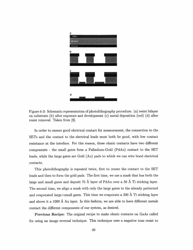
ensuring good liftoff. This process is illustrated in Fig. 4-3.
39
A
b
Figure 4-3: Schematic representation of photolithography procedure. (a) resist bilayer
on substrate (b) after exposure and development (c) metal deposition (red) (d) after
resist removal. Taken from [9].
In order to ensure good electrical contact for measurement, the connection to the
SETs and the contact to the electrical leads must both be good, with low contact
resistance at the interface. For this reason, these ohmic contacts have two different
components - the small gates form a Palladium-Gold (PdAu) contact to the SET
leads, while the large gates are Gold (Au) pads to which we can wire bond electrical
contacts.
This photolithography is repeated twice, first to create the contact to the SET
leads and then to form the gold pads. The first time, we use a mask that has both the
large and small gates and deposit 75 A layer of PdAu over a 50 A Ti sticking layer.
The second time, we align a mask with only the large gates to the already patterned
and evaporated large+small gates. This time we evaporate a 200 A Ti sticking layer
and above it a 1000 A Au layer. In this fashion, we are able to have different metals
contact the different components of our system, as desired.
Previous Recipe: The original recipe to make ohmic contacts on GaAs called
for using an image reversal technique. This technique uses a negative tone resist to
40

create an undercut profile. Instead of exposing the feature where the metal is desired,
the areas around the feature are exposed However, this process is highly sensitive to
a certain baking temperature and we did not get consistent results when this process
was transferred to a silicon substrate. -
We therefore decided to use positive tone resist. In order to change photolithog-
raphy recipes, we had to order a suitable positive mask. Additionally, only four to six
mesas were patterned at a time on a small GaAs sample. We designed a 5 inch mask
suitable for a 4 inch wafer. The mask contained a 10 by 10 array of mesas; 100 mesas
total. Two mask were made, one with both the small and large gates and one with
just the large gates. Future mask design should include alignment and orientation
markers outside the array of mesas to aid in the alignment of the large gates with the
small gates.
The natural SiO2 layer on top of any silicon sample makes it hard for metals
evaporated on a Si substrate to stick to the surface. We encountered difficulty in
getting the PdAu to stick directly to silicon substrate so we had to deposit a Ti
sticking layer first, which was not the case for our old GaAs.
4.2 Electron Beam Lithography
In electron beam lithography, a beam of electron rasters a pattern across a substrate
coated with a sensitive resist layer. The beam reacts with the resist, exposing it. Once
developed, the exposed resist is removed, creating a mask through the substrate.
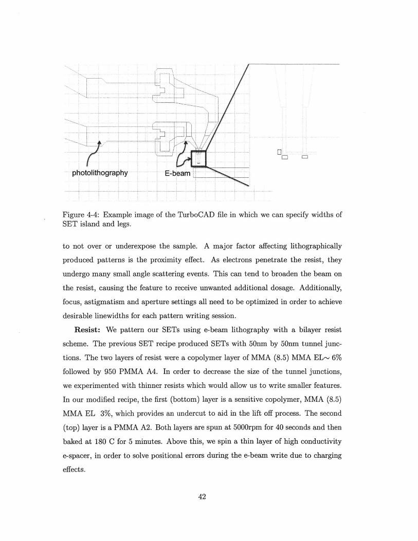
TurboCAD is used to make the file which contains the pattern to be written
using e-beam. It is easy to modify this pattern, making it possible to write patterns
with many different leg and island widths in order to see which ones would have the
smallest tunnel junctions and thus the highest charging energy. An example of a
single SET is shown in Fig. 4-4.
To optimize pattern resolution, it is necessary to vary beam parameters affecting
the sample, including current and dosage. Usually a trial and error process guided
by the known material parameters is required to optimize these parameters so as
41
photolithography E-bEm
Figure 4-4: Example image of the TurboCAD file in which we can specify widths ofSET island and legs.
to not over or underexpose the sample. A major factor affecting lithographically
produced patterns is the proximity effect. As electrons penetrate the resist, they
undergo many small angle scattering events. This can tend to broaden the beam on
the resist, causing the feature to receive unwanted additional dosage. Additionally,
focus, astigmatism and aperture settings all need to be optimized in order to achieve
desirable linewidths for each pattern writing session.
Resist: We pattern our SETs using e-beam lithography with a bilayer resist
scheme. The previous SET recipe produced SETs with 50nm by 50nm tunnel junc-
tions. The two layers of resist were a copolymer layer of MMA (8.5) MMA EL- 6%
followed by 950 PMMA A4. In order to decrease the size of the tunnel junctions,
we experimented with thinner resists which would allow us to write smaller features.
In our modified recipe, the first (bottom) layer is a sensitive copolymer, MMA (8.5)
MMA EL 3%, which provides an undercut to aid in the lift off process. The second
(top) layer is a PMMA A2. Both layers are spun at 5000rpm for 40 seconds and then
baked at 180 C for 5 minutes. Above this, we spin a thin layer of high conductivity
e-spacer, in order to solve positional errors during the e-beam write due to charging
effects.
42

Exposure Parameters: We write the SET features using a beam current (rate
of electron charge deposition) of 5OpA. The pattern is written with a resolution of
60,000 dots in a 75pm by 75 pm area. During each write session, we must optimize the
aperture settings as well as the focus and stigmation for the desired beam current.
It is also necessary to check that the height of the sample and thus the focus of
the beam does not vary too much in different areas of the sample. After adjusting
the focus and stigmation, we must align the e-beam pattern to the already present
photolithography pattern of the gates on the sample. The SETs are exposed with a
dose of 1750 pC/cm2 corresponding to a dose time of 0.55 ps/dot. This dose time
depends on the beam current with which the features are being written as well as the
intensity of the beam.
4.3 Shadow Evaporation
Metal is deposited on a substrate using thermal evaporation. The evaporation proce-
dure for the photolithography step is fairly standard. Now I describe the evaporation
process used to make tunnel junctions that is performed after e-beam lithography.
After e-beam exposure on a bilayer resist coated wafer, the substrate is developed,
removing the exposed resist. This creates an undercut resist profile where the top
resist layer is suspended over the bottom. Separate layers of metal are deposited in
an evaporator at oblique angles, a process known as shadow evaporation, in order to
make small area tunnel junctions [3]. We use the evaporator in the Yacoby Group
in which the sample can be mounted on a stage where we can control the polar and
azimuthal angles. To optimize the dimensions of our tunnel junctions, it is necessary
to determine the most advantageous angles at which to perform the evaporation.
Our shadow evaporation procedure is such that during the first evaporation we
wish to deposit metal only into the island of the SET. The deposited metal is then
oxidized to form the tunnel barrier. The second evaporation is meant to fill in the
legs of the SET and form tunnel junctions at the overlapping points between the legs
and the island. A schematic is shown in Fig. 4-5.
43

2nd evaporation
Legs
island
1 s evaporation
Tunnel junctions
Figure 4-5: Schematic of an SET with the legs connected via tunnel junctions to theisland. Explains the evaporation procedure.
During the first evaporation, we wish to evaporate at a polar angle larger than the
critical angle such that we can choose to only deposit metal on the island of the SET
and no metal is deposited in the legs. Fig. 4-6 shows a schematic of the cross section
of the resist profile for the leg of an SET. The mask consists of the copolymer layer
of resist with thickness 51 and the resist layer with the desired pattern of thickness
J2. The size of the exposed region, labeled by w, corresponds to the width of the
SET leg. From basic trigonometry we see that the critical angle depends only on the
width of the feature and the thickness of the suspended resist layer, with
6c = arctan - . (4.1)J2
First the island is created by evaporation of Aluminum at a polar angle of 0 =
450 and an azimuthal direction parallel to the island trench, say 4 = 00. At this
evaporation angle, 112 A of Al is deposited. The tunnel barrier is then formed by
oxidizing a thin layer of the Aluminum deposited on the island. The island is exposed
to dry air at a pressure of 2.6 torr for 5.5 minutes, creating an 1nm thick insulating
oxide layer. The sample is then rotated by an azimuthal angle of # = 90* such that
the legs are now parallel to the evaporation direction. To form the legs, 162 A of Al
44

'W
Figure 4-6: Schematic showing the first evaporation of shadow evaporation procedurefor an SET leg. At this stage of the evaporation we only want to deposit metal intothe island and not into the legs. For this to occur, the angle of evaporation must beat least the critical angle.
is deposited. See Fig. 4-5 and Fig. 4-6.
The resistance and capacitance of the tunnel junction will depend on the thickness
of the oxide, and thus the amount of oxidation time, as well as the overlap area
between evaporation steps.
The liftoff is carried out using by immersing the sample in boiling acetone.
4.4 Dose Test
In order to calibrate a new e-beam recipe, we must first perform a dose test to de-
termine the optimal dose at which the pattern should be written. The dose, charge
per surface area measured in pC/cm2 , is analogous to the exposure time. A dose test
involves writing the SET (without the leads.) at various doses in order to determine
the optimal dose. This dose test pattern is written twice on one sample which is then
cleaved. On one of the samples, we perform a standard, polar angle 0 = 0* evap-
oration, while the other sample we evaporate using the shadow evaporation process
described above. An example of a dose test pattern is shown in Fig. 4-7. This pattern
is written at different doses, giving us the ability to see which dose and island size
works best.
We then image the SETs using a Scanning Electron Microscope (SEM), looking
45

Figure 4-7: SEM image of a dose test pattern that is repeated at several differentdoses in order to determine optimal dose.
for the dose which leads to the smallest feature size that is completely formed and
closest to the widths specified in the pattern file. Overexposed images tend to be
wider than specified, with features that are not as sharp.
From such a dose test, we were able to determine that the dose time of 0.55 ps/dot
for the SETs works best since the SET island widths that most closely matched the
widths of the file. For higher doses times (0.70 and 0.82 ps/dot), islands still looked
good, but were much wider than expected width based on file. An example of this is
shown in Fig. 4-8
4.5 Resist Thickness and Angle Determination
In order to figure out the optimal polar angle at which to perform our shadow evap-
oration, it is necessary to first determine the thickness of our resist. We measure
the resist thicknesses in two ways: using a Vecco Optical Profilometer and using an
SEM. We spin a layer of resist on a silicon chip and use the SEM to expose a square
region of the resist. The profilometer has a tip which quantitatively measures the
surface profile. As the tip scans across the exposed region of our sample, we are able
to obtain a measure of the resist thickness. To measure the resist thickness using an
SEM, we spin a layer of resist on a chip and expose a cross using e-beam lithography.
46
Island width 40nm leg width
20nm F E
25nm4
30nm
35nm
40nm

Figure 4-8: SEM image illustrating the optimal results from the dose test. An angleevaporation with a polar angle of 450 was performed. We compare widths measuredin the SEM to the ones specified by the files used for the e-beam. In the write file,the SET islands had a width of 30nm. For a dose time of 0.55ps/dot, islands weremeasured using an SEM to have a width of 34nm. For a dose time of 0.70ps/dot,islands were measured using an SEM to have a width of 42nm.
47

(a) (b)0 < 6c
Figure 4-9: Shadow Evaporation less than critical angle. (a) shows a schematic of theSET legs during the first evaporation. The first evaporation is meant to only depositmetal in the island, but here (for angles less than the critical angle) we see that somemetal is deposited in the legs as well. This leads to the shorting of the island to thelegs as can be seen in the SEM image of the SET (b).
We place the sample of a 45 degree sample holder and measure the shadow seen at a
45 degree tilt due to the thickness of the resist.
We find the MMA EL3 layer to be -50nm and the PMMA A2 to be ~50nm as
well. During the first evaporation we wish to only deposit metal in the island and not
the legs. The SET legs in our file are at most w = 40nm wide, which gives a critical
angle of 380. To be safe, since the resist profiles are not necessarily sharp rectangles,
we perform our evaporations at a polar angle of 45'.
Fig. 4-9 shows SETs that were evaporated at a polar angle 0 = 350, an angle less
than the critical angle. The first evaporation from the right seemed to come in at too
steep an angle depositing some metal into the legs even though our intention was to
only deposit metal in the island. The extra metal deposited in the legs due to not
enough shadowing, leads to the doubling of the legs, causing several of the SETs to
be shorted. We also have trouble with liftoff, shown in Fig. 4-10, if there is metal
stuck to the walls of the undercut layer. This can occur if the incorrect evaporation
angle is used.
48

Figure 4-10: A mesa with 15 SETs where the liftoff was not successful. Most of thee-beam pattern is still covered in metal from the evaporation.
Figure 4-11: SEM image of an SET written without having optimal focus and stig-mation. Island and legs are not continuous.
4.6 Focus and Alignment Problems
Fig. 4-11 shows an SET written without having optimal focus and stigmatic. The
island and legs are not continuous and the tunnel junctions have not been formed.
Fig. 4-12 illustrates good versus bad alignment. In order to electrically test these
SETs we must have good photolithography and good alignment of the SET pattern to
the photolithography pattern. In the case of bad alignment, the SET legs are shorted
together rendering any electrical testing of these SETs useless.
49

Figure 4-12: SEM image showing the comparison between (a) bad alignment and(b)good alignment of the e-beam step to the photolithography one. In the case of (a)we would not be able to make electrical contact to the SET and so would not be able
to test the SETs.
4.7 Successful SETs
After optimizing all these different parameters, we had several successes of SETs.
Fig. 4-13 shows the smallest island and leg widths that we have been able to achieve
using e-beam lithography. We were able to obtain features as small as 30nm by 30nm
tunnel junctions. However, the ohmic contacts on this sample did not come out well,
as shown in the SEM image of the mesa in Fig. 4-14. Therefore we were not able to
make electrical contact to the SETs. Thus we were not able to measure the electric
characteristics of these SETs.
Fig. 4-15 shows the device that has islands 35nm wide and legs 40nm wide.
Unlike the previous sample, the ohmic contacts were well aligned to the SETs, and
we were able to make good electrical contacts. Therefore, we measured these SETs
in a dilution refrigerator. The SET characterization measurements are discussed in
the following chapter.
50

MIT. 20W 98WAW~m DStFb02- WO- 7*0 Vim tewbU0 Thmt*2
200m ENT .0 W MU A Am Deb *i.Fb 2O2Ptb M. - W4 1w ~~4
Figure 4-13: Compare file parameters to measured feature size. (a) File parametersfor the SET are 25nm wide island and 30nm wide legs. On the SEM, we measure30nm wide islands and 30nm wide legs. (b) File parameters are 35nm wide islandand45 nm wide legs. On the SEM, we measure 37nm wide islands and 45nm widelegs.
Figure 4-14: The SETs on this mesa were very good, but the small gates made withphotolithography did not come out. Thus we were not able to make electrical contactto the SETs.
51
45 nm
37 nm
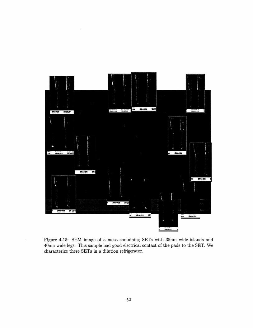
Figure 4-15: SEM image of a mesa containing SETs with 35nm wide islands and40nm wide legs. This sample had good electrical contact of the pads to the SET. Wecharacterize these SETs in a dilution refrigerator.
52

Chapter 5
SET Characterization
Transport measurements are used to characterize the SETs. In this chapter, I first
describe preliminary measurements of the SET resistance. By measuring the resis-
tance and conductivity for different applied voltages or currents, we can determine
the functioning of the SET devices. Next, I describe the measurements performed
in a dilution refrigerator. We measure Coulomb oscillations and Coulomb blockade
diamonds by sweeping the bias and gate voltages. From these measurements we can
obtain values for several parameters of the SET as well as determine the charge sensi-
tivity of the device. The charge sensitivity is the charge variation that can be detected
in a certain measurement time window where the precision improves as the square
root of the measurement time.
5.1 Preliminary Measurements
We perform some preliminary resistance measurements at liquid helium temperatures
of 4K. Measuring the resistance of the SET is the simplest way to determine whether
the SETs have functioning tunnel junctions or are defunct either due to shorted leads
or broken leads.
We mount the sample onto a chip carrier and wire bond the ohmic contacts on
the chip to pins on the chip carrier. The chip carrier is then inserted into a Helium
dewar. We determine the resistance of the SETs from the characteristic current-
53

voltage curves of the device measured using a parameter analyzer. We apply a DC
bias voltage between the source and drain of the SET while grounding the gate. By
sweeping the bias voltage and measuring the current through the SET, we can obtain
an I-V curve for the device. For the old SET recipe, resistances of about 300kOhm
were measured whereas the resistances of new SETs fall in the range of 2-5MOhms. In
our new SET recipe, we have decreased the area of the tunnel junctions significantly,
so we expect the resistance of the device to increase.
At 4K we tried to measure Coulomb Oscillations but were not able to resolve
the periodic jumps in current due to the tunneling of a single electron. The most
likely explanation is that the temperature was not low enough, thus the condition
Ec/ggkBT was not satisfied, and so we were not able to see any discernible features
in the data.
Therefore, we then tested our samples in a dilution fridge. The measurements and
data of our SETs, taken in a dil fridge at a temperature of 10mK, is presented in the
following sections.
5.2 Measurement of Coulomb Blockade in SETs
In order to measure the SETs at temperatures lower than 4K, we perform transport
measurements on our sample loaded into a dil fridge. In this section, we present
several measurements of Coulomb Oscillations and Coulomb Diamonds with the dil
fridge at a base temperature of ~ 10mK. From measurements of the conductance
(I/V) and differential conductance (dI/dV)of the SETs, we are able to obtain an esti-
mate for the charging energy and the various capacitances of the SET. Additionally,
we also measure the charge sensitivities of these devices.
Coulomb Oscillations: Individual electrons tunneling through the aluminum
oxide barrier, hopping onto the island from one lead and off the island to the other
lead gives rise to a current flow. This current flow, as described in Chapter 3, is not
continuous, but has a peak each time the an additional electron tunnels onto and then
off the island. The periodic nature of the current can be seen by fixing the source-
54
drain voltage and sweeping the gate voltage, which modulates the chemical potential
of the island. Fig. 5-1 (a) and (b) present sample data for such Coulomb oscillations in
current in one of our SETs. Coulomb Diamonds: We can also observe the effect of
sweeping both the gate voltage and the bias voltage of the SET. If we plot bias voltage
as a function of gate voltage, we see characteristic Coulomb diamonds depicting the
coulomb blockade region. In this region no current flows through the SET because
the electrons cannot overcome the charging energy of the island. This 2D stability
plot is shown in Fig. 5-1 (c) and (d). The DC current measurements measure I vs.
V directly, whereas the AC current measurements give a direct measure of dI/dV,
which can be seen by taking a Taylor expansion.
Determination of Capacitances from Coulomb Diamonds: From these
Coulomb diamonds, we can extrapolate several parameters as described in Chapter 3.
We see that the Coulomb diamonds are approximately equally spaced by AVJ ~
12mV, which is the voltage that needs to be applied in order to change the island
charge by one electron. The gate capacitance can be obtained from AV, as was
calculated in Eq. 3.13. This gives C = e/AVq ~ 13aF. The height of the diamond
is proportional to the charging energy, giving Ec = e2/2C - 0.85meV. A charging
energy of 0.85meV corresponds to a temperature of - 10K. From these two values,
assuming that the capacitances of the source and the drain are approximately the
same, we get Cs = CD ~ 41aF.
Another way to estimate the source and drain capacitances is using the slopes
of the Coulomb Diamond. During our measurement, we ground one of the legs of
the SET (the drain) and apply all of our bias voltage to the other leg (the source).
The slopes of the Coulomb diamonds are estimated from Fig. 5-1 and using the value
for C - 13aF calculated earlier. The positive slope is estimated to be Vs/V
C/(C, + CD) - 0.85mV/3.7mV ~ 0.2125 and the negative slope is estimated to be
Vs/V = -C/CS~ -0.85mV/3.2mV ~ -0.2656. These values of the slopes yield
a source capacitance of CD = 43aF and a drain capacitance of Cs = 45aF. Having
determined all the capacitances, we can now estimate the charging energy. The total
capacitance of the dot is CE = C1 + C2 + CG. C = 101aF yielding a charging energy
55
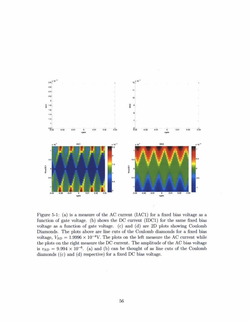
120"
10
0.01 02 0.03 St03 0,02 -001
x.6
1.S
0.5
0Vgale
0.01 0.02 0.03
0.
0
-05
vg4
Figure 5-1: (a) is a measure of the AC current (IAC1) for a fixed bias voltage as afunction of gate voltage. (b) shows the DC current (IDC1) for the same fixed biasvoltage as a function of gate voltage. (c) and (d) are 2D plots showing CoulombDiamonds. The plots above are line cuts of the Coulomb diamonds for a fixed biasvoltage, VSD = 1.9996 x 10- 4 V. The plots on the left measure the AC current whilethe plots on the right measure the DC current. The amplitude of the AC bias voltageis VSD = 9.994 x 10⁻⁶. (a) and (b) can be thought of as line cuts of the Coulombdiamonds ((c) and (d) respective) for a fixed DC bias voltage.
56
2.8 x 10-"
2.8
24
2
1.6
1.4
12
03 02 -001 0vgate
0.1
vga
X2
D

of Ec = e2/2C, ~ 0.80meV. This is approximately the value read off directly from
the stability diagram for the diamond height.
5.3 Charge Sensitivity of SETs
Next, I discuss the two different measurements of the charge sensitivity of these SETs.
The typical trace of the dc current as a function of the gate voltage for a fixed
bias voltage is shown in Fig. 5-2(b). It shows the Coulomb blockaded regions where
the current is zero and the tunneling region where a single electron tunnels across
the junction. As the gate voltage is tuned, the current increases from zero, reaches
a maximum and decreases again. In order to measure the charge sensitivity, it is
necessary to wiggle the system at a given gate voltage by adding a small ac component
to the gate voltage. The fluctuations in the voltage generate fluctuations or noise in
the current. These current fluctuations are a measure of the susceptibility of the
system; the higher the susceptibility the greater the sensitivity of the system.
In the first measurement, the charge sensitivity of the SET is determined by
measuring the difference in noise between the current flow and the Coulomb blockade
regime. In order to do so, we first fix the bias voltage, VSD. We add a constant
AC gate voltage and sweep the DC portion of the gate voltage to measure current
through the SET, shown in Fig. 5-2. The plot on the right, (b) shows Coulomb
oscillations, i.e. a measure of the DC current through the SET as a function of gate
voltage as mentioned above. The plot on the left (a) shows the behavior of the AC
current through the SET as a function of gate voltage and is essentially a measure
of the noise on the Coulomb oscillations shown in (b). The AC gate voltage induces
an electron to tunnel generating the sharp tunneling resonances observed in the AC
current. It is interesting to see that the fluctuations are smallest in the blockade
region as one might have expected but they are also reduced at the peak of the dc
current. The charge fluctuations are maximum on the rise and fall of the dc current
which is reasonable because that is when the current is changing the most. The ac
signal is therefore sensitive not to the value of the dc current but to the derivative of
57
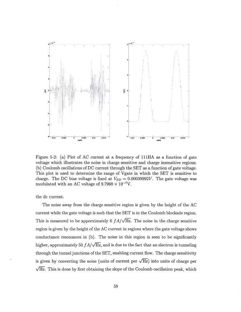
m lat w 1 0"
44
2.
-
0 -- -
-0.01 -0.005 0 0006 0.01 0,011 .001 -OW 0 001 0.015
Figure 5-2: (a) Plot of AC current at a frequency of crnHA as a function of gatevoltage which illustrates the noise in charge sensitive and charge insensitive regions.(b) Coulomb oscillations of DC current through the SET as a function of gate voltage.This plot is used to determine the range of Vgate in which the SET is sensitive tocharge. The DC bias voltage is fixed at VSD = o.00039992V. The gate voltage wasmodulated with an AC voltage of 9.7968 x 10⁷IV.
the dc current.
The noise away from the charge sensitive region is given by the height of the AC
current while the gate voltage is such that the SET is in the Coulomb blockade region.
This is measured to be apporximately 6 fA/VrHiz. The noise in the charge sensitive
region is given by the height of the AC current in regions where the gate voltage shows
conductance resonances in (b). The noise in this region is seen to be significantly
higher, approximately 50 fA/Vii-, and is due to the fact that an electron is tunneling
through the tunnel junctions of the SET, enabling current flow. The charge sensitivity
is given by converting the noise (units of current per v/H~:) into units of charge per
viz. This is done by first obtaining the slope of the Coulomb oscillation peak, which
58

gives us current in terms of the gate voltage. Then we use the conversion factor that
one charge e corresponds to a change in gate voltage AV = 12mV as seen from the
Coulomb diamonds. Thus the charge sensitivity is:
noise 50f A/Vnoise -50fIVH~ 2.2 x 10~4 e(5.1);V * Vg" 1.3 x 10- 8A/V x 12mV/e 22 ' (.
Next we perform a different measurement in order to get another estimate of the
noise on the current. In this measurement, the goal is to determine the AC gate
voltage at which we will no longer be able to resolve the noise on the DC current
through the SET. For this measurement, we fix the bias voltage on the SET and
sweep the DC and AC gate voltages while recording the DC and AC current. Fig. 5-3
shows a 2D plot of AC current (left) and DC current(right) as a function of DC gate
voltage on the x-axis and AC gate voltage on the y-axis. As we sweep the DC gate
voltage, we expect to see a Coulomb oscillation. Fig. 5-3(b) shows this peak in the
DC current due to the electron tunneling through the tunnel junctions of the SET. In
order to resolve the noise in the current, we modulate the gate voltage (by applying
an AC voltage) and look at its effects on the current modulation (by measuring the
AC current). When the AC gate voltage is on the order of the noise in the current,
we are no longer able to resolve an AC current through the SET. We see from Fig. 5-3
(a) that the AC current signal disappears around 3 x 10~6V, giving us our noise. We
then convert this noise (in units of V) into units of charge, using the conversion factor
that one charge e corresponds to a change in gate voltage of AV = 12mV. Each
point is taken for an integration time of 1s. Thus our charge sensitivity is:
noise 1 3 x 10- 6 V 4 eA~qe /~002V ~ 2.5 x 10- (5.2)AV,|e V/-z0.012V/e v*-
This is a pretty remarkable charge sensitivity, demonstrating why SETs can be
used as extremely sensitive charge sensors, as is the case in this experiment.
59
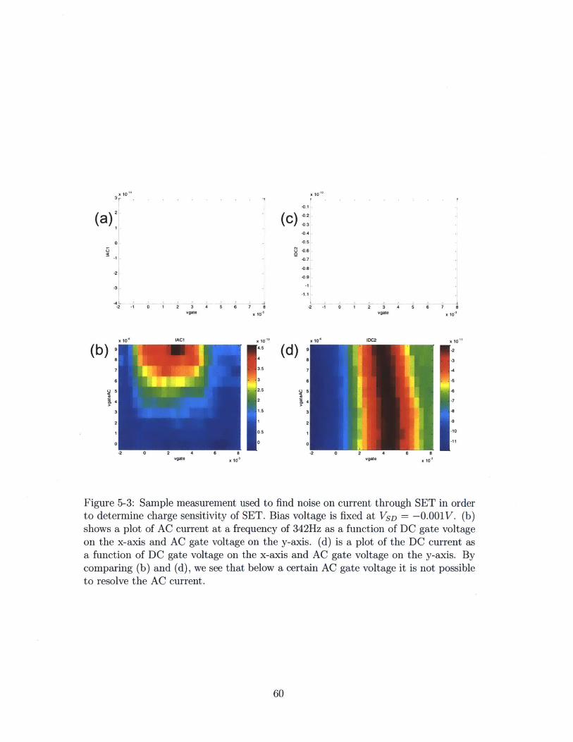
X 10"
.01
(c):0.4
.0.5
.0.6
0.7
0.8
0,9
*2 .v 0 1 2 3 4vows
IAC1
5 7 0
X 10:1
X 10"
45
3.535
2.5
2
1.5
0.5
0
(d)
-1.1
X 10,
vgW. X 10
0 1 2 3 4 5 6vga.
0C2
vg X 10
Figure 5-3: Sample measurement used to find noise on current through SET in orderto determine charge sensitivity of SET. Bias voltage is fixed at VSD = -0.001V. (b)shows a plot of AC current at a frequency of 342Hz as a function of DC gate voltageon the x-axis and AC gate voltage on the y-axis. (d) is a plot of the DC current asa function of DC gate voltage on the x-axis and AC gate voltage on the y-axis. Bycomparing (b) and (d), we see that below a certain AC gate voltage it is not possibleto resolve the AC current.
60
X 1043~.
(a)2
U
-I
.3
X 10
(b)
X 10"
X 101,
.2
.3
4
.7
4-8
-10
*1 I
4

5.4 Future Testing
The data presented above was taken in a dil fridge at a base temperature of -10
mK. During the warming up of the dil fridge, we did not have very good control of
the temperature, and so were not able to measure these SETs at around 1K or 2K.
We ultimately want our SETs to be fully functional at -2K in a helium cryostat.
Once the cryostat arrives at the end of may, we will test these SETs to see if they
work at that temperature. But since a charging energy of 0.85meV corresponds to a
temperature of 10K, we are hopeful that these SETs will show discernible coulomb
oscillations with a relatively good charge sensitivity at temperatures of 2K.
61

Chapter 6
Conclusion
In this thesis, I have described the start of our study of using phosphorus doped silicon
as a semiconductor qubit. The ultimate goal of the experiment is to use a novel hybrid
technique that combines the advantages of spin selective optical excitations with those
of electrical readout measurements to detect the spin state of a single electron. This
thesis focuses on the fabrication of SETs which can be used to electrically detect the
final charge of the P donor and determine whether the donor remained neutral or was
excited and formed a P+ ion via the Auger process. I have been able to overcome the
challenges associated with fabricating SETs that can be operated in the 2K regime.
This necessitated minimizing the tunnel junction areas through optimized lithography
and evaporation techniques. Through considerable experimentation, I was able to
fabricate SETs with very narrow features, the most successful run yielding SETs
with 30nm wide legs and a 30nm wide island.
We performed transport measurements in a dil fridge in order to characterize
these SET devices. We were able to measure Coulomb oscillations and Coulomb
blockade diamonds for these SETs. We find that these SETs have a charging energy
of approximately Ec ~ 0.85meV which corresponds to a temperature of about 10K.
Additionally, we measure the charge sensitivity of the SETs to be ~ 2 x 10-e/ VH .
We are pretty confident that these SETs will show discernible Coulomb oscillations
with relatively good charge sensitivity at temperatures of 2K. The SETs will be tested
in our helium cryostat, in which the experiment will be performed, once it arrives.
62

SETs are extremely versatile in their applications. They can be used as very
sensitive charge detectors as in the larger experiment described in the thesis. They
can also be used as very precise temperature sensors as well as magnetometers. Thus
the ability to fabricate SETs with higher operating temperatures opens the door to
many possible experiments. This could pave the way to further probe fascinating
properties of semiconducting systems.
63

Appendix A
SET Fabrication Recipes
A.1 Photolithography of Optical Gates
Small and Large Gates
" prebake Si wafer 180 0C for 3 min" Resist LOR 3A" Spin 5000 rpm for 40 sec" Bake 180*C for 5 min" Resist S1805" Spin 5000 rpm for 40 sec" Bake 115*C for 5 min" Expose using MA 6 for 4.0 sec" Develop in CD-26 for 60 sec" Rinse with DI and blow-dry
" Evaporate" 50 A Ti sticking layer" 75 A PdAu" Liftoff" PG Remover 60'C for 6 hours" Rinse with DI and blow-dry
Large Gates
prebake Si wafer 180*C for 3 minResist LOR 20BSpin 5000 rpm for 40 secBake 180*C for 5 minResist S1805Spin 5000 rpm for 40 secBake 115*C for 5 minExpose using MA 6 for 4.0 secDevelop in CD-26 for 60 secRinse with DI and blow-dry
Evaporate200 A Ti sticking layer1000 A AuLiftoffPG Remover 60'C for 6 hoursRinse with DI and blow-dry
64

A.2 Ebeam Lithography
Resist Spinning
" MMA EL3 made by diluting MMAEL6 with Ethyl Lactate in a 1:1 ra-tio
" Copolymer MMA EL3" Spin 5000rpm 40sec" Bake 180*C 5 min" Resist PMMA A2" Spin 5000 rpm 40 sec" Bake 180*C 5 min" E-spacer" Spin 2000 rpm 40 sec" No bake
Elionix Parameters
" Current = 50pA" Dose: SET = 0.55, Pads =0.5, Ucut
= 0.2
Development
e Dip in DI H20 for 20sec to removee-spacer
" Develop in MIBK (sitting on ice for
10 min) for 60sec" Rinse with IPA and blow-dry
Shadow Evaporation
" Purge 02 line before beginningevaporation
" Set polar angle to 450" Set azimuthal angle parallel to is-
land (evaporation from the right)
" Evaporate 45 A Al (actually 112 Adue to Xtal monitor conversation)
" Wait 10 min. for metal to cool
" Process gas 02 at 2.6 mbar, 5.5 min" Set azimuthal angle parallel to legs
(evaporation from the top)" Evaporate 65 A Al (actually 162 A
due to xtal monitor conversion)" Wait 10 min for metal to cool
" Liftoff in boiling acetone
65

Bibliography
[1] N.W. Ashcroft and N.D. Mermin. Solid State Physics. Saunders College Pub-lishing, Fort Worth, 1976.
[2] M. H. Devoret and R. J. Schoelkopf. Amplifying quantum signals with the singleelectron transistor. Nature, 406:1039-1046, 2000.
[3] G. J. Dolan. Offset masks for lift-off photoprocessing. Applied Physics Letters,31:5, 1977.
[4] A. Yang et. al. Optical detection and ionization of donors in specific electronicand nuclear spin states. Phys. Rev. Lett, 97:227401, 2006.
[5] B. E. Kane et. al. Single spin measurement using single-electron transistors toprobe two-electron systems. Phys. Rev. B., 61:2961, 2000.
[6] L. Kouwenhoven et. al. Single electron charging effects in semiconductor quantumdots. Z. Phys. B - Condensed Matter, 85:367-373, 1991.
[7] T. A. Fulton and G. J. Dolan. Observation of single-electron charging effects insmall tunnel junctions. Phys. Rev. Lett, 59:109, 1987.
[8] G. Grosso and G.P. Parravicini. Solid State Physics. Elsevier Academic Press,Amsterdam, 2000.
[9] S. Hickman. Liftoff photoresist processing. cns.f as.harvard.edu/facilities/docs/SP112_r1_1_\X20LOR.pdf.
[10] T. Ihn. Semiconductor Nanostructures - Quantum States and Electronic Trans-port. Oxford University Press, New York, 2010.
[11] B. E. Kane. A silicon-based nuclear spin quantum computer. Nature, 393:133,1998.
[12] M. A. Kastner. Artificial atoms. Physics Today, 46:24, 1993.
[13] M. A. Kastner. The single electron transistor and artificial atoms. Annalen derPhysik, 9:885-894, 2000.
[14] C. Kittel. Introduction to Solid State Physics. John Wiley and Sons, Amsterdam,8th edition, 2005.
66

[15] L. Kouwenhoven and C. Marcus. Quantum dots. Physics World, 1998.
[16] Y. Nakamura, C. Chen, and J. Tsai. 100-k operation of al-based single electrontransistors. Japan Appl. Phys., 35:1465-1467, 1996.
[17] Y. A. Pashkin, Y. Nakamura, and J. S. Tsai. Room-temperature al single-electrontransistor made by electron-beam lithography. Applied Physics Letters, 76:16,2000.
[18] M. Y. Simmons. Probing dopants at the atomic level. Nature Physics, 4:165,2008.
[19] D. Sleiter, N. Y. Kim, K. Nozawa, T.D. Ladd, M. L. W. Thewalt, and Y. Ya-mamoto. Quantum hall charge sensor for single-donor nuclear spin selection insilicon. New Journal of Physics, 12, 2010.
[20] L. Sohn, L. Kouwenhoven, and G. Schon, editors. Mesoscopic Electron Transport.Kluwer Academic Publishers, Dordrecht, 1997.
[21] Silicon Crystal Structure. http://hyperphysics.phy-astr.gsu.edu/hbase/solids/sili2.html.
[22] A. M. Tyryshkin, S. A. Lyon, A. V. Astashkin, and A. M. Raitsimring. Electronspin relaxation times of phosphorus donors in silicon. Phys. Rev. B, 68:193207,2003.
67