Embed Size (px)
Citation preview

Application Report SWPA221– September 2012
1
SD/MMC Debug Guidelines T. BELGHITH OPBU/SPE/HW Application
ABSTRACT
The purpose of this document is to help root causing and solving issues related to SD/MMC.
This document is dedicated to OMAP44xx devices but many tips can be used for other OMAP devices as the SD/MMC interface is standardized.
Document History Version Date Author Notes
1.0 August 2012 T. BELGHITH First release
1.1 August 2012 T. BELGHITH Changes after review
1.2 September 2012 T. BELGHITH Changes after last review
SWPA221
2 SD/MMC Debug Guidelines
WARNING: EXPORT NOTICE
Recipient agrees to not knowingly export or re-export, directly or indirectly, any product or technical data (as defined by the U.S., EU, and other Export Administration Regulations) including software, or any controlled product restricted by other applicable national regulations, received from Disclosing party under this Agreement, or any direct product of such technology, to any destination to which such export or re-export is restricted or prohibited by U.S. or other applicable laws, without obtaining prior authorization from U.S. Department of Commerce and other competent Government authorities to the extent required by those laws. This provision shall survive termination or expiration of this Agreement. According to our best knowledge of the state and end-use of this product or technology, and in compliance with the export control regulations of dual-use goods in force in the origin and exporting countries, this technology is classified as follows: US ECCN: 3E991 EU ECCN: EAR99 And may require export or re-export license for shipping it in compliance with the applicable regulations of certain countries.
SWPA221
SD/MMC Debug Guidelines 3
Contents 1 PBIAS Configuration .................................................................................................................... 4
Sequence to configure the PBIAS Cell: .......................................................................................... 5 2 Pull-up Values............................................................................................................................... 6
2.1 Internal pull-up Values Supported by MMC1 Interface ............................................................ 7 2.2 Pull-up Values Requested by MMC Standard: ........................................................................ 7 2.3 Pull-up Values Requested by SD Standard ............................................................................ 7 2.4 Pull-up Values Requested by eMMC Standard ....................................................................... 8
3 SD/MMC Debug Experiences ....................................................................................................... 8 3.1 No MMC Communication ........................................................................................................ 8 3.2 Overshoots/Undershoots on SDMMC Signals ........................................................................ 9 3.3 SD/MMC is Not Booting .......................................................................................................... 9 3.4 SD/MMC Card Not Detected ................................................................................................. 10 3.5 No Command Complete Received ........................................................................................ 10 3.6 Setup Timing Issue ............................................................................................................... 10 3.7 MMC Signals Interrupted ...................................................................................................... 12 3.8 How to Handle the SD/MMC Bus With a Busy State? ........................................................... 13 3.9 Cards Format Supported by OMAP ...................................................................................... 13
References.......................................................................................................................................... 14
Figures Figure 1: Power-up Sequence vs PWRDNZ ........................................................................................ 4 Figure 2: Example of a Bad Power Sequence Management Creating a Bad Behavior on SD/MMC12
Tables Table 1. Power supplies ................................................................................................................ 5 Table 2. CONTROL_MMC1[31]SDMMMC1_PUSTRENGTH_GRP0 bit field ................................. 6 Table 3. MMC1 internal Pull-up values ......................................................................................... 7 Table 4. Pull-up values from the MMC standard vs internal pull-up ........................................... 7 Table 5. Pull-up values form SD standard vs internal pull-up .................................................... 7 Table 6. Pull-up values form eMMC standard vs internal pull-up ............................................... 8 Table 7. MMC1_CONTROL.SDMMC1_DRx_SPEEDCTRL bit field .............................................. 9 Table 8. MMC/SD/SDIO 1 Interface Standard SD Mode ............................................................. 11 Table 9. MMC/SD/SDIO 1 Interface High Speed SD/SDR50/DDR50 Mode ................................ 11 Table 10. MMC/SD/SDIO 2 Interface High Speed DDR/SDR JC64 Mode ..................................... 12
SWPA221
4 SD/MMC Debug Guidelines
In this document, ‘SD/MMC interface’ expression is used to refer to OMAP interface that drives the SD, SDIO and eMMC peripheral.
Note: It is recommended reading the OMAP4430 Silicon Errata Public (3) in addition to this document.
1 PBIAS Configuration
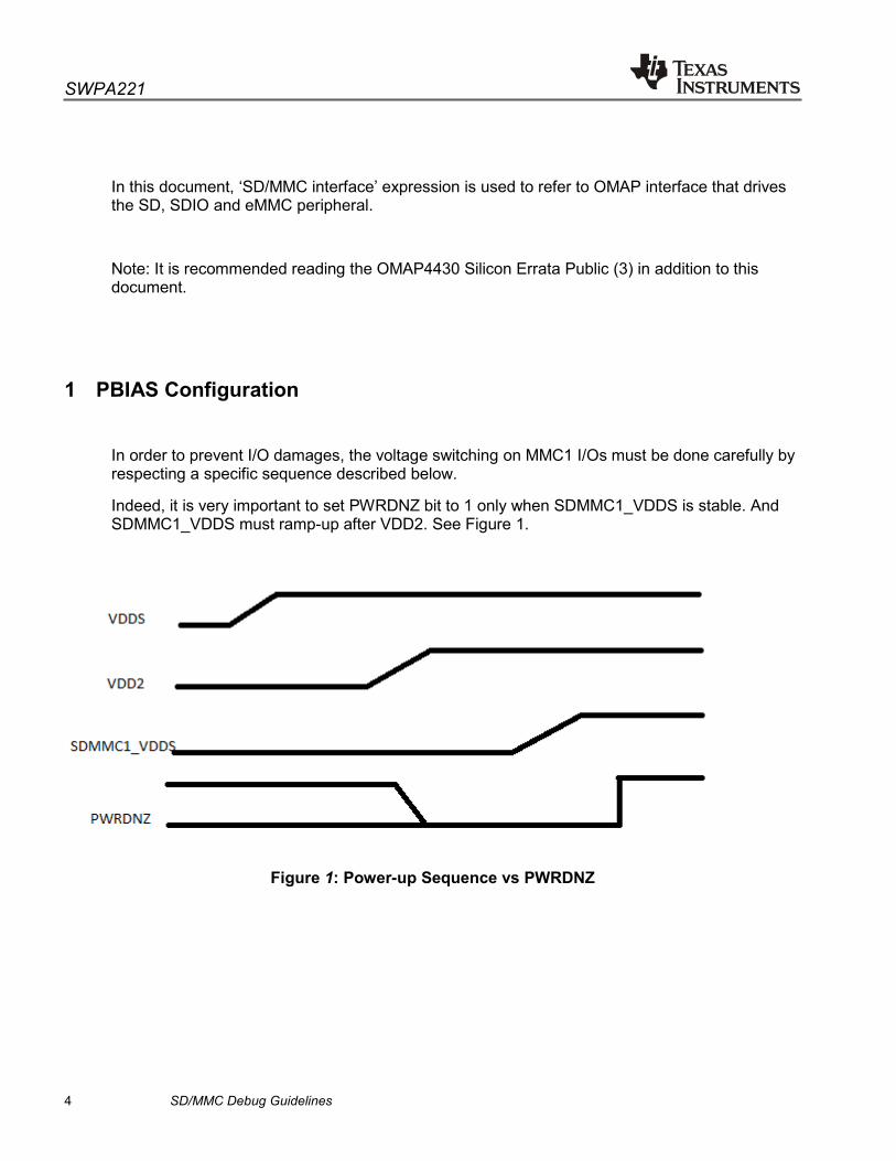
In order to prevent I/O damages, the voltage switching on MMC1 I/Os must be done carefully by respecting a specific sequence described below.
Indeed, it is very important to set PWRDNZ bit to 1 only when SDMMC1_VDDS is stable. And SDMMC1_VDDS must ramp-up after VDD2. See Figure 1.
Figure 1: Power-up Sequence vs PWRDNZ

SWPA221
SD/MMC Debug Guidelines 5
Table 1. Power Supplies
Sequence to configure the PBIAS Cell:
1. PWRDNZ allows protecting the MMC1 PBIAS cell and MMC1 I/O cell when SDMMC1_VDDS is not stable (ramp)
Enable PWRDNZ mode for PBIAS cell and MMC1 IO cell :
CONTROL_PBIASLITE[22] MMC1_PBIASLITE_PWRDNZ = 0.
CONTROL_PBIASLITE[26] MMC1_PWRDNZ = 0.
2. Preliminary setting for PBIAS and MMC1 IO cells:
Enable MMC1 PBIAS cell output:
Set CONTROL_PBIASLITE[25]MMC1_PBIASLITE_HIZ_MODE = 0
Configure pin muxing for MMC1.
Depending on the max clock speed used, configure CONTROL_MMC1.SDMMC1_DRx_SPEEDCTRL bits.
If no external pull-ups are used on the board then choose the internal pull-up value with CONTROL_MMC1.SDMMC1_PUSTRENGTH_GRPx bits (see section pull-up values on MMC bus).
3. Program the power IC to generate the required voltage (1.8V or 3V) to SDMMC1_VDDS
4. The PBIAS voltage is given by the VMODE bit value, so VMODE bit must be set according to SDMMC1_VDDS voltage:
Configure CONTROL_PBIASLITE[21] MMC1_PBIASLITE_VMODE.
5. Wait and ensure that the voltage of SDMMC1_VDDS is stable (ramp-up is ended and configured voltage is reached) before jumping to next step.
6. Generate the PBIAS voltage by disabling PBIAS PWRDNZ and enable the MMC1 extended IO cell by disabling the MMC1 PWRDNZ:

SWPA221
6 SD/MMC Debug Guidelines
Set CONTROL_PBIASLITE[22] MMC1_PBIASLITE_PWRDNZ =1.
Wait 150us; // 150us: min time between PBIAS powerup and PBIAS output stable
Set CONTROL_PBIASLITE[26] MMC1_PWRDNZ = 1.
7. For debug purpose, store the SUPPLY_HI_OUT bit state (CONTROL_PBIASLITE[24]) in memory.
8. Check PBIAS and MMC1 IO VMODE_ERROR values (or enable the PBIAS_ERROR interrupt).
If VMODE_ERROR is high then power-down the IOs for protecting them:
– Set CONTROL_PBIASLITE[26] MMC1_PWRDNZ = 0 and set CONTROL_PBIASLITE[22]MMC1_PBIASLITE_PWRDNZ =0.
Check SUPPLY_HI_OUT value stored at step 7 corresponds to the desired SDMMC1_VDDS voltage.
If the values corresponds then change the VMODE bit (CONTROL_PBIASLITE[21]) to the correct value.
If they differ, then correct the VDDS_MMC1 voltage.
2 Pull-up Values
eMMC, SDIO and SD cards must have pull-up on the Data and CMD lines in order to prevent bus floating.
MMC1 interface allows using internal pull-ups by selecting values in CONTROL_MMC1.SDMMMC1_PUSTRENGTH_GRPx register field. See example of register field below:
Table 2. CONTROL_MMC1[31]SDMMMC1_PUSTRENGTH_GRP0 bit field
Their value covers the Rcmd and Rdat (Command and Data signals) pull-up range for SD, MMC and eMMC standards. For MMC the standard requires Rcmd=50kOhms, thus CONTROL_MMC1.SDMMMC1_PUSTRENGTH_GRPx bit field will be set to ‘1’ when using MMC1 interface for MMC purpose.
SWPA221
SD/MMC Debug Guidelines 7
2.1 Internal pull-up Values Supported by MMC1 Interface
The max internal pull-up value is 110kOhms, it is 10kohms higher than the SD/MMC/eMMC standards but the difference in term of current is not high (~2-3uA). If you use this range with 110kOhms then you’ll have to check the timings.
Parameter Symbol Min Max Unit Pull-up resistance for CMD
Rcmd 10 110 kOhm
Pull-up resistance for DAT0-7
Rdat 10 110 kOhm
Table 3. MMC1 internal Pull-up values
2.2 Pull-up Values Requested by MMC Standard:
Parameter Symbol Min Max Unit Remark Pull-up resistance for CMD
Rcmd 4.7 100 kOhm Value supported by MMC1 internal pull-up
Pull-up resistance for DAT0-7
Rdat 50 100 kOhm Value supported by MMC1 internal pull-up
Table 4. Pull-up Values from the MMC Standard vs Internal Pull-up
2.3 Pull-up Values Requested by SD Standard
Parameter Symbol Min Max Unit Remark Pull-up resistance for CMD
Rcmd 10 100 kOhm Value supported by MMC1 internal pull-up
Pull-up resistance for DAT0-7
Rdat 10 100 kOhm Value supported by MMC1 internal pull-up
Table 5. Pull-up Values form SD Standard vs Internal Pull-up
SWPA221
8 SD/MMC Debug Guidelines
2.4 Pull-up Values Requested by eMMC Standard
Parameter Symbol Min Max Unit Remark Pull-up resistance for CMD
Rcmd 4.7 100 kOhm Value supported by MMC1 internal pull-up
Pull-up resistance for DAT0-7
Rdat 10 100 kOhm Value supported by MMC1 internal pull-up
Table 6. Pull-up values form eMMC standard vs internal pull-up
3 SD/MMC Debug Experiences In below sections, different scenarios of issues are described and a corresponding way to treat them is suggested.
3.1 No MMC Communication
If no transaction has been done between OMAP and the SD/MMC device, then first take some captures of the MMC bus signals (CMD and CLK) and a register dump of MMC module.
• Check the power voltage of SDMMC1_VDDS
• Check the VMODE_ERROR bit for MMC1
• Check whether at least one command has been sent on the bus by observing either the waveform captures or the SD/MMC registers.
A timeout in the MMCHS_STAT register may reflect that a command has been sent but no answer has been received from the SD/MMC peripheral. It means that the host sent a command or data to the device. So, the host has been configured successfully for sending a command but not necessarily in term of IOs. If no waveform is available for proving that a clock and a command are sent to the device then we need to check the IO pad configuration (mux mode, pull-up).
• Check also the external clock frequency.
If no transfer is done and no signal is output on the bus, then use the register dump for checking that the clock divider (MMCHS_SYSCTL[15:6] CLKD) has the correct value and check also the clock source of the functional clock. Ensure that the clock is provided to the card (MMCHS_SYSCTL[2] CEN=1) and that the module is enabled (CM_L3INIT_HSMMC1_CLKCTRL[1:0]Modulemode=0x2).
• You can use the MMCHS_CON.CLKEXTFREE bit to enable a free running clock on the SD/MMC bus and verify with an oscilloscope that it is toggling.

SWPA221
SD/MMC Debug Guidelines 9
3.2 Overshoots/Undershoots on SDMMC Signals
Overshoots and undershoots may appear in the SD/MMC bus if the impedance adaptation was not done correctly or when EMI coupling occurs.
When overshoots or undershoots are reported on SD/MMC signal lines we have to be care that they will not disturb the behavior or damage OMAP IOs.
The occurrence and the voltage level of these perturbations are information needed for the debug.
Indeed, if undershoots occur while SD/MMC transfers are on-going then they may be interpreted as bit transitions when the level is close to the Vih/Vil of OMAP I/O.
In that case some error such as CRC errors will be detected during the transfers.
In case of overshoots, the level should not exceed VDDS+0.3V. This is the max voltage supported by the SD/MMC IOs.
The best way to minimize the overshoots/undershoots consists of adapting the lines impedance. Changing the serial resistor value (increasing it) has often a significant impact.
The other parameter which could be used is the MMC1_CONTROL.SDMMC1_DRx_SPEEDCTRL. This bit controls the drive strength and it can be changed to the value ‘0’ for decreasing the I/O strength and undershoots/overshoots.
Table 7. MMC1_CONTROL.SDMMC1_DRx_SPEEDCTRL bit field
3.3 SD/MMC is Not Booting
OMAP has the capability to boot from SD/MMC devices depending on the sysboot configuration.
If the boot doesn’t occur from the device, then some basic checks are needed:
• Check that the chosen sysboot configuration covers SD/MMC booting
• Check that the external pull-ups used for the sysboot configuration are strong enough (less than 3kOhms).
• Check that SDMMC1_VDDS voltage is present during the boot.

SWPA221
10 SD/MMC Debug Guidelines
After all these checking, if the issue still occurs then try to boot from a different peripheral (i.e. UART or USB). No need to boot completely with such devices but at least you should see ASIC ID printed in the UART terminal window. If nothing is displayed with the different boot mode then the other OMAP power supplies should be checked or the OMAP device may be damaged.
If you are seeing that the boot skips the SD/MMC and boot from the following device in the sysboot configuration then you are probably facing a power ramp-up issue.
Indeed, the SDMMC1_VDDSshould ramp in less than 90us, otherwise ROM code will skip the SD/MMC booting since the voltage is not stabilized. In such case, the ramp delay must be decreased.
3.4 SD/MMC Card Not Detected
SD/MMC cards have usually a dedicated pin named CD in the connector level. For allowing the card detection, this pin is tied to GND as soon as the card is inserted in the connector.
The default state of this pin must be in the high state. So, in case of card detect issue, ensure that a pull-up is present on that CD pin.
Then, on its other side this CD pin should be connected to either a GPIO (with wake-up capability) or to the CD input of the PMIC. The SW is then in charge of detecting the corresponding interrupt. The SW is responsible of the detection so, some issue may come from the bad GPIO reading from the SW.
3.5 No Command Complete Received
After a command is sent to the SD/MMC device, then the Host should receive a response with a status. The command is considered as sent completely and successfully only after receiving the response from the SD/MMC device and the command complete (CC) bit is set.
If the command is sent to the SD/MMC device but the response of that command did not issue a command complete assertion then a timeout occurs.
In case of no CC is set then there are some assumptions:
• The command has not been sent by OMAP (see ‘No MMC communication)
• The card is in a bad state:
– Check the power of the card
– Check the pull-up are enabled and their values
3.6 Setup Timing Issue
OMAP SD/MMC timings definition has been done using a trace length range and load range.

SWPA221
SD/MMC Debug Guidelines 11
SD/MMC Setup or Hold timings may be violated on a board if the trace lengths or loads are out of the range. If the setup time is too short then it may be needed to increase the length of the traces.
So, the schematic and layout review should be done with respect to these constraints. See below tables.
PCB Conditions Value
Min Max unit
Number of external peripherals 1
Far end load 40 pF
Trace length for SD card types 10 cm
Characteristics impedance ScanDisk Extreme III cards 45 55 ohms
Other card types 20 70
Table 8. MMC/SD/SDIO 1 Interface Standard SD Mode
PCB Conditions Value
Min Max unit
Number of external peripherals 1
Far end load 10 pF
Trace length for SD card types 10 cm
Characteristics impedance ScanDisk Extreme III cards 45 55 ohms
Other card types 20 70
Table 9. MMC/SD/SDIO 1 Interface High Speed SD/SDR50/DDR50 Mode

SWPA221
12 SD/MMC Debug Guidelines
PCB Conditions Value
Min Max unit
Number of external peripherals 1
Far end load 5 pF
Trace length for SD card types 5 cm
Characteristics impedance 30 55 ohms
Table 10. MMC/SD/SDIO 2 Interface High Speed DDR/SDR JC64 Mode
3.7 MMC Signals Interrupted
Some SD/MMC issues may not be due directly to the SD/MMC controller but from other parameters like bad power management sequences.
The consequence of a bad power management sequence on SD/MMC could be a stop of transfer without consistent explanation found in the register dump analysis. Figure below illustrate that case.
Another consequence is an interruption of the SD/MMC signals sometimes during a transfer.
Figure 2: Example of a Bad Power Sequence Management Creating a Bad Behavior on SD/MMC
SWPA221
SD/MMC Debug Guidelines 13
In the case shown in the figure above, the VDD_MPU is at OPP100 while VDD_CORE is at OPP50. This is a forbidden configuration because of the OPP dependencies (see OMAP44xx DM Operating Conditions Addendum). The consequence of this bad configuration creates some instability in the SD/MMC controller.
3.8 How to Handle the SD/MMC Bus With a Busy State?
To be able to send a command, the bus must not be in busy state, the Host has to wait the end of busy state.
It is recommended to set the MMCHS_CMD.RSP_TYPE register field to 0x3 (“48 bit response with busy after response”). This will allow the controller to set the timeout bit (CTO) when the busy state stays too long.
Only the command CMD13 can be sent to the card while the bus is in busy state.
The command CMD13 (“Send status”) can be used for getting the state of the card.
In order to know the bus state, it’s not advised sending repeatedly CMD13 since it takes time and BW but you can check first the state of MMCHS_STAT[1].TC bit. It will tell if a transfer is complete. If that bit is at ‘0’ (“Transfer not complete”) then you have to check the register MMCHS_PSTATE[2].DLA (rather than the bit DLEV) to know whether the bus is busy or not.
There is no big difference between MMCHS_PSTATE[DLA] and MMCHS_PSTATE[DLEV] but it is preferable using the DLA bit because it is more trustful since it consider the state of the Host(active/inactive), and not only the state of the line (1 or 0 level).
3.9 Cards Format Supported by OMAP
It is stated in the OMAP4 TRM that the max card size supported is 32GB. But depending on the card type, OMAP4 can support higher capacity.
Indeed, the SDHC (SD High Capacity) format standard specifies a max capacity of 32GB and uses the FAT32 system file. But there is another format, named SDXC (SD eXtended Capacity) which allows up to 2TB capacity. But this card format uses a different system file which is the exFAT.
So, to conclude, the limitation doesn’t come from the HW but rather from the SW. OMAP4 can support SDXC format if the SW is adapted to the exFAT system file.

SWPA221
14 SD/MMC Debug Guidelines
References
1. OMAP4430 Multimedia Device Silicon Revision 2.x (SWPU231AH) 2. OMAP4430 Multimedia Device Engineering Sample Version D (SWPS041D) 3. OMAP4430 Silicon Errata Public Version M (SWPZ009M)

IMPORTANT NOTICE
Texas Instruments Incorporated and its subsidiaries (TI) reserve the right to make corrections, enhancements, improvements and otherchanges to its semiconductor products and services per JESD46, latest issue, and to discontinue any product or service per JESD48, latestissue. Buyers should obtain the latest relevant information before placing orders and should verify that such information is current andcomplete. All semiconductor products (also referred to herein as “components”) are sold subject to TI’s terms and conditions of salesupplied at the time of order acknowledgment.
TI warrants performance of its components to the specifications applicable at the time of sale, in accordance with the warranty in TI’s termsand conditions of sale of semiconductor products. Testing and other quality control techniques are used to the extent TI deems necessaryto support this warranty. Except where mandated by applicable law, testing of all parameters of each component is not necessarilyperformed.
TI assumes no liability for applications assistance or the design of Buyers’ products. Buyers are responsible for their products andapplications using TI components. To minimize the risks associated with Buyers’ products and applications, Buyers should provideadequate design and operating safeguards.
TI does not warrant or represent that any license, either express or implied, is granted under any patent right, copyright, mask work right, orother intellectual property right relating to any combination, machine, or process in which TI components or services are used. Informationpublished by TI regarding third-party products or services does not constitute a license to use such products or services or a warranty orendorsement thereof. Use of such information may require a license from a third party under the patents or other intellectual property of thethird party, or a license from TI under the patents or other intellectual property of TI.
Reproduction of significant portions of TI information in TI data books or data sheets is permissible only if reproduction is without alterationand is accompanied by all associated warranties, conditions, limitations, and notices. TI is not responsible or liable for such altereddocumentation. Information of third parties may be subject to additional restrictions.
Resale of TI components or services with statements different from or beyond the parameters stated by TI for that component or servicevoids all express and any implied warranties for the associated TI component or service and is an unfair and deceptive business practice.TI is not responsible or liable for any such statements.
Buyer acknowledges and agrees that it is solely responsible for compliance with all legal, regulatory and safety-related requirementsconcerning its products, and any use of TI components in its applications, notwithstanding any applications-related information or supportthat may be provided by TI. Buyer represents and agrees that it has all the necessary expertise to create and implement safeguards whichanticipate dangerous consequences of failures, monitor failures and their consequences, lessen the likelihood of failures that might causeharm and take appropriate remedial actions. Buyer will fully indemnify TI and its representatives against any damages arising out of the useof any TI components in safety-critical applications.
In some cases, TI components may be promoted specifically to facilitate safety-related applications. With such components, TI’s goal is tohelp enable customers to design and create their own end-product solutions that meet applicable functional safety standards andrequirements. Nonetheless, such components are subject to these terms.
No TI components are authorized for use in FDA Class III (or similar life-critical medical equipment) unless authorized officers of the partieshave executed a special agreement specifically governing such use.
Only those TI components which TI has specifically designated as military grade or “enhanced plastic” are designed and intended for use inmilitary/aerospace applications or environments. Buyer acknowledges and agrees that any military or aerospace use of TI componentswhich have not been so designated is solely at the Buyer's risk, and that Buyer is solely responsible for compliance with all legal andregulatory requirements in connection with such use.
TI has specifically designated certain components which meet ISO/TS16949 requirements, mainly for automotive use. Components whichhave not been so designated are neither designed nor intended for automotive use; and TI will not be responsible for any failure of suchcomponents to meet such requirements.
Products Applications
Audio www.ti.com/audio Automotive and Transportation www.ti.com/automotive
Amplifiers amplifier.ti.com Communications and Telecom www.ti.com/communications
Data Converters dataconverter.ti.com Computers and Peripherals www.ti.com/computers
DLP® Products www.dlp.com Consumer Electronics www.ti.com/consumer-apps
DSP dsp.ti.com Energy and Lighting www.ti.com/energy
Clocks and Timers www.ti.com/clocks Industrial www.ti.com/industrial
Interface interface.ti.com Medical www.ti.com/medical
Logic logic.ti.com Security www.ti.com/security
Power Mgmt power.ti.com Space, Avionics and Defense www.ti.com/space-avionics-defense
Microcontrollers microcontroller.ti.com Video and Imaging www.ti.com/video
RFID www.ti-rfid.com
OMAP Applications Processors www.ti.com/omap TI E2E Community e2e.ti.com
Wireless Connectivity www.ti.com/wirelessconnectivity
Mailing Address: Texas Instruments, Post Office Box 655303, Dallas, Texas 75265Copyright © 2012, Texas Instruments Incorporated


![(e)MMC/SD/SDIO State of Affairsconnect.linaro.org.s3.amazonaws.com/sfo17... · First MMC stack by Russell King in kernel 2.6.9 [MMC] Add MMC core](https://img.dokumen.tips/doc/110x75/5f5ee69463a1e67f0c5f43dc/emmcsdsdio-state-of-first-mmc-stack-by-russell-king-in-kernel-269-mmc-add.jpg)