Embed Size (px)
Citation preview
OLED Activities

© CEA. All rights reserved
LETI / Display Lab | 2
Leti at a Glance Founded in 1967 as part of CEA
1,700 researchers
50 start-ups & 365 industrial partners
Over 1,880 patents
250 M€ budget
CEO Dr. Laurent Malier
210 PhD students + 30 post PhD with 85 foreign students (35%)
~ 30M€ CapEx
273 generated in 2011 40% under license
© CEA. All rights reserved
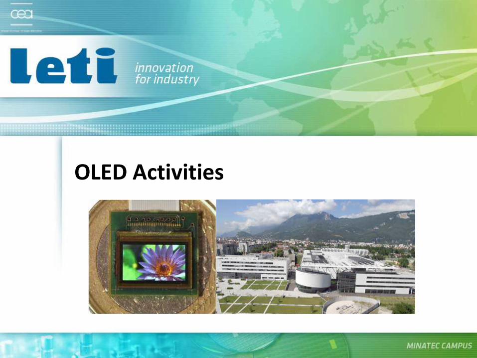
Main activities in Optoelectronics
Department of Optics and PhoTonics
Photonic on Silicon
• Photonics technologies and components for optical com.
LED
• GaN Led technologies
•LED lighting systems
•Oleds technologies
Displays
•OLED microdisplays
•Optical projection systems
Imagerie
•Vis APS
•IR HgCdTe & InSb photodiodes
•IR Bolometers
Optical sensors
•Infra red spectroscopies for gaz sensing
© CEA. All rights reserved
LETI / Display Lab | 4
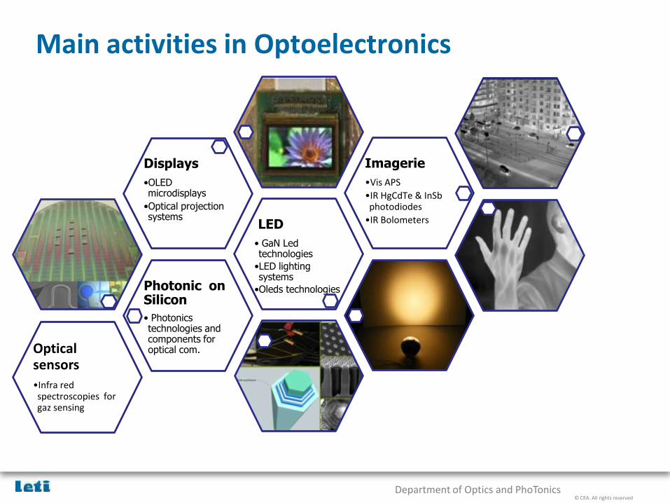
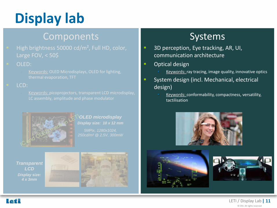
Display lab Components
High brightness 50000 cd/m², Full HD, color, Large FOV, < 50$
OLED: Keywords: OLED Microdisplays, OLED for lighting,
thermal evaporation, TFT
LCD: Keywords: picoprojectors, transparent LCD microdisplay,
LC assembly, amplitude and phase modulator
OLED microdisplay
Display size: 10 x 12 mm
5MPix, 1280x1024,
250cd/m² @ 2,5V, 300mW
Transparent
LCD
Display size:
4 x 3mm
System
Systems 3D perception, Eye tracking, AR, UI,
communication architecture
Optical design Keywords: ray tracing, image quality, innovative optics
System design (incl. Mechanical, electrical design) Keywords: conformability, compactness, versatility,
tactilisation
© CEA. All rights reserved
LETI / Display Lab | 5
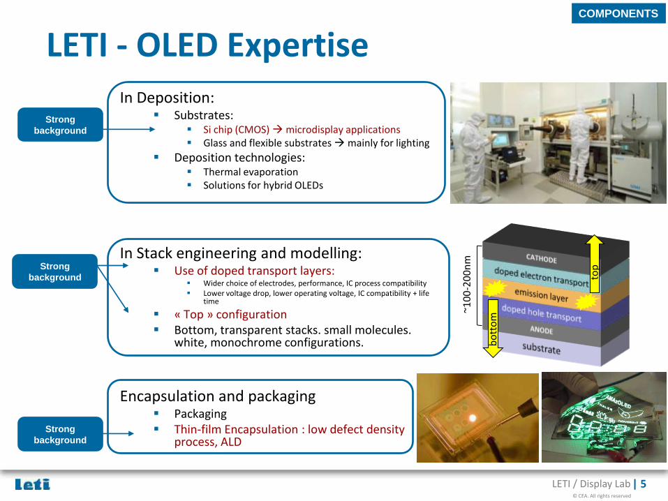
LETI - OLED Expertise In Deposition:
Substrates: Si chip (CMOS) microdisplay applications Glass and flexible substrates mainly for lighting
Deposition technologies: Thermal evaporation Solutions for hybrid OLEDs
In Stack engineering and modelling: Use of doped transport layers:
Wider choice of electrodes, performance, IC process compatibility Lower voltage drop, lower operating voltage, IC compatibility + life
time
« Top » configuration Bottom, transparent stacks. small molecules.
white, monochrome configurations.
Encapsulation and packaging
Packaging Thin-film Encapsulation : low defect density
process, ALD
Strong
background
Strong
background
Strong
background
COMPONENTS
top
bo
tto
m ~1
00
-20
0n
m

© CEA. All rights reserved
LETI / Display Lab | 6
Focus on OLED evaporation tools
rg
Substrate holder
Shadow mask
Organic
materials sources heaters
Load
lock
Glove box
(encapsulation)
Transfer
chamber
(robot)
Buffer
chamber
Sputtering
chamber :
(ITO, SiO2) Metal
deposition
chamber
Plasma
chamber
Size : 3x5m
Organic
deposition
chamber Organic
deposition
chamber
COMPONENTS
Cluster SUNIC
LESKER Super Spectros
© CEA. All rights reserved
LETI / Display Lab | 7
PACKAGING
Color filters
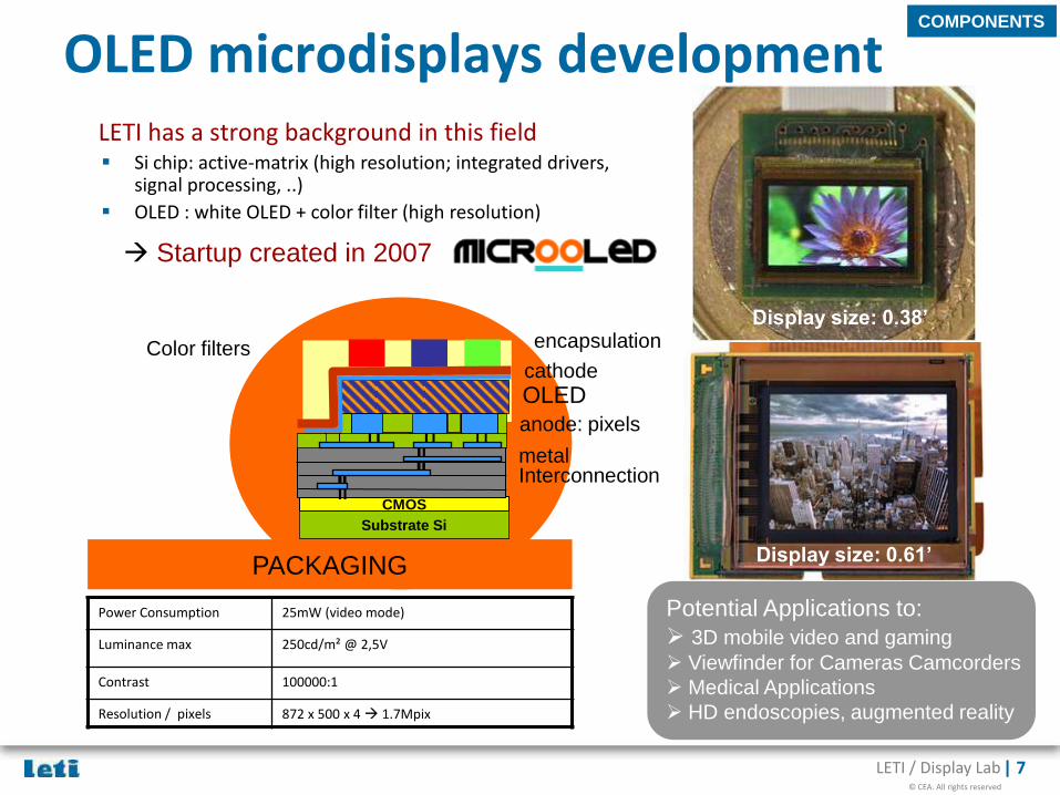
LETI has a strong background in this field
OLED microdisplays development
Substrate Si
CMOS
metal Interconnection
anode: pixels
OLED cathode
encapsulation
Startup created in 2007
Display size: 0.38’
Power Consumption 25mW (video mode)
Luminance max 250cd/m² @ 2,5V
Contrast 100000:1
Resolution / pixels 872 x 500 x 4 1.7Mpix
Potential Applications to:
3D mobile video and gaming
Viewfinder for Cameras Camcorders
Medical Applications
HD endoscopies, augmented reality
Si chip: active-matrix (high resolution; integrated drivers, signal processing, ..)
OLED : white OLED + color filter (high resolution)
Display size: 0.61’
COMPONENTS

© CEA. All rights reserved
LETI / Display Lab | 8
OLED lighting OLED for lighting:
Transparent OLED – glass substrate – 50 x 50mm²
Partnership with OSRAM
‘ON’ state: white light emission ‘OFF’ state: transparency
Color tunable OLED: OLED stripes Substrate: Si - Dimension: 22 x 18 mm²
COMPONENTS
© CEA. All rights reserved
LETI / Display Lab | 9
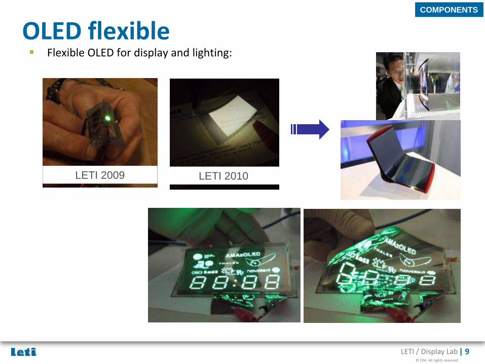
OLED flexible Flexible OLED for display and lighting:
LETI 2009 LETI 2010
COMPONENTS

© CEA. All rights reserved
LETI / Display Lab | 10
Hybrid OLEDs
ITO/Glass
PEDOT/PSS (HIL)
Red QDs
ETL
Ag
Inkjet
Spin coating
Evaporation
Red Quantum Dots (CdSe) as emitters
Develop hybrid QD-LEDs for sources and detectors in the visible range and up to 3µm 2 layers out of solution:
COMPONENTS
HTL: Hole transport layer
HBL: Hole blocking layer
ETL: Electron transport layer
0,096cm² 4cm²
© CEA. All rights reserved
LETI / Display Lab | 11
Display lab Components
High brightness 50000 cd/m², Full HD, color, Large FOV, < 50$
OLED: Keywords: OLED Microdisplays, OLED for lighting,
thermal evaporation, TFT
LCD: Keywords: picoprojectors, transparent LCD microdisplay,
LC assembly, amplitude and phase modulator
OLED microdisplay
Display size: 10 x 12 mm
5MPix, 1280x1024,
250cd/m² @ 2,5V, 300mW
Transparent
LCD
Display size:
4 x 3mm
System
Systems 3D perception, Eye tracking, AR, UI,
communication architecture
Optical design Keywords: ray tracing, image quality, innovative optics
System design (incl. Mechanical, electrical design) Keywords: conformability, compactness, versatility,
tactilisation
© CEA. All rights reserved
LETI / Display Lab | 12
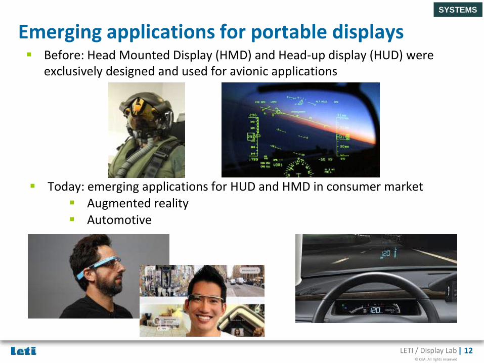
Before: Head Mounted Display (HMD) and Head-up display (HUD) were exclusively designed and used for avionic applications
Emerging applications for portable displays
Today: emerging applications for HUD and HMD in consumer market Augmented reality Automotive
SYSTEMS
© CEA. All rights reserved
LETI / Display Lab | 13
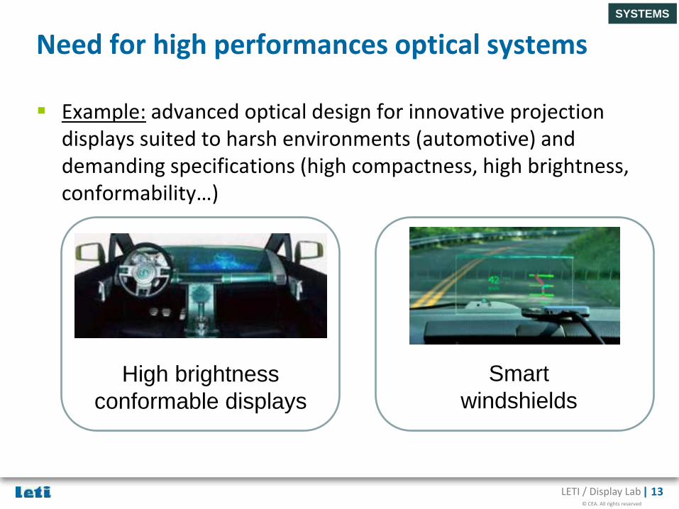
Example: advanced optical design for innovative projection displays suited to harsh environments (automotive) and demanding specifications (high compactness, high brightness, conformability…)
Need for high performances optical systems
High brightness
conformable displays
Smart
windshields
SYSTEMS

Innovation for industry