Embed Size (px)
Citation preview

Ohmic Contacts for High TemperatureIntegrated Circuits in Silicon Carbide
KATARINA SMEDFORS
Licentiate Thesis in Information and Communication TechnologyKTH, Royal Institute of Technology
Stockholm, Sweden 2014
TRITA-ICT/MAP AVH Report 2014:19ISSN 1653-7610ISRN KTH/ICT-MAP/AVH-2014:19-SEISBN 978-91-7595-352-6
KTH School of Information andCommunication Technology
SE-164 40, KistaSWEDEN
© Katarina Smedfors, December 2014
Tryck: Universitetsservice US AB

I
Abstract in English In electrical devices and integrated circuits, ohmic contacts are necessary and a
prerequisite for the current transport over the metal-semiconductor junctions. At the same time, a desired property of the ohmic contacts is to not add resistance or in other way disturb the performance. For high temperature electronics, the material demands are high regarding functionality and stability at elevated working temperatures, during and after temperature cycling and during long time of use.
Silicon carbide, SiC, is a suitable substrate material for fabrication of high temperature electronics with a large band gap, good thermal conductivity and chemical inertness. The large bandgap causes however difficulties in finding a common material for ohmic contacts to both n- and p-type SiC. The goal of this project is to find a suitable metallization for n- as well as p-type contacts to epitaxially doped SiC for use in integrated circuits. The circuit technology developed and used in KTH for SiC is built on bipolar junction transistors. The p-doped base layer in the transistors is relatively low doped; 5 x 10¹⁷ – 1 x 1018 cm-3. P-type SiC is more difficult to form ohmic contacts to than n-type SiC, with such a low doping concentration it is even more complicated.
Today, the metallizations used in the contacts consists of Ni for n-type contacts and Ni/Ti/Al to p-type SiC. Experiments of the specific contact resistivity ρc and the sheet resistance Rsh of these contacts, characterized to two types of samples, are presented for the extreme temperature range of -40 °C – 500 °C. Ohmic contact test chips with transfer length method structures have been compared to similar test structures on samples from the KTH SiC integrated circuits. The metals were also tested on the opposite doping polarity.
Sputter deposition of Co and Si in layers to form CoSi2 contacts was made to chips from the same contact test wafer for comparison with the behavior of the presently used contacts. Since this was a new metallization, the process development of the high temperature anneal and contact formation made an important part of the work.
Out of the tested contacts, Ni has been the best for n-SiC and Ni/Ti/Al for p-SiC. None of the three metallizations formed ohmic contacts to both n- and p-SiC. However, the CoSi2 contacts showed specific contact resistivity ρc <4 x 10⁻⁶ Ωcm2 at 25 °C and non-linear I-V characteristics but without barriers to p-SiC after voltage sweeps of ± 75V.

II
Svensk sammanfattning I elektriska komponenter och integrerade kretsar är ohmska kontakter en
nödvändighet och förutsättning då de möjliggör strömtransport över metall-halvledarövergångar. Samtidigt är en önskvärd egenskap att de varken tillför resistans eller på annat sätt stör prestandan. För högtemperaturselektronik ställer det stora krav på val av material vad gäller funktion och stabilitet vid höga arbetstemperaturer, vid temperaturcyklingar samt under längre tids belastning.
Kiselkarbid, SiC, är ett lämpligt substratmaterial för tillverkning av högtemperaturselektronik med sitt stora bandgap, goda värmeledningsförmåga och kemiska inerthet. Det stora bandgapet orsakar dock svårigheter i ett gemensamt materialval för ohmska kontakter både till n- och p-dopad SiC. Målet med detta projekt är att hitta en lämplig metallisering för ohmska kontakter till epitaxiellt n- och p-dopad SiC för användning i integrerade kretsar. De integrerade kretsar som utvecklats och tillverkas vid KTH är baserade på bipolära transistorer. Det p-dopade baslagret i dessa transistorer är relativt lågdopade, 5 x 10¹⁷ – 1 x 1018 cm-3. P-dopad SiC är svårare att tillverka ohmska kontakter till än n-dopad, en så låg dopningskoncentration gör det ännu mer komplicerat.
De idag använda kontaktmetalliseringarna består av Ni för kontakter till n-SiC och Ni/Ti/Al för kontakter till p-SiC. Experiment av specifika kontaktresistiviteten ρc och ytresistansen Rsh av dessa kontakter på två typer av prov presenteras för det extrema temperaturintervallet -40 °C – 500 °C. Testchip för ohmska kontakter med strukturer tillverkade enbart för kontakttester har där jämförts med liknande teststrukturer på prover tillhandahållna från kretstillverkningen. Samma metaller testades också på motsatt dopningspolaritet.
Med sputterdeponerade lager av Co och Si tillverkades CoSi2-kontakter till n-SiC på chip för kontakttester från samma skiva för jämförelsen med de idag använda kontakterna. Eftersom detta var en ny metallisering utgjorde utformandet av en lämplig värmebehandling för silicideringen en viktig del av arbetet.
Av de testade kontakterna var Ni bäst för n-typ och Ni/Ti/Al för p-typ. Ingen av de tre metalliseringarna har fungerat på både n- och p-SiC. CoSi2-kontakter gav dock en specifik kontaktresistivitet på ρc <4 x 10⁻⁶ Ωcm2 vid 25 °C och icke-linjära I-V kurvor men utan barriärer på p-typ efter potentialsvep ± 75V.

III
Acknowledgement It has been some interesting and educative years invested in this licentiate and I have been introduced to the, for me totally new, fields of microelectronics and especially silicon carbide electronics. I am grateful to my two supervisors, main supervisor Prof. Carl-Mikael Zetterling and co-supervisor Prof. Mikael Östling, for accepting me as a doctoral student in this fascinating project and sharing your extensive knowledge of the field.
For his always kind help with measurements and generous input as internal reviewer of this thesis, I truly want to thank Prof. Gunnar Malm.
Most of this work – processing, measurements and SiC in general – was introduced to me by Dr. Luigia “Gina” Lanni who has not only taught me a lot and showed how hard work pays off in results, but has also become a great friend, in Electrum and during our trips.
Without the help and discussions with Docent Per-Erik Hellström Dr. Gabriel Roupillard, Dr. Thomas Zabel and Dr. Christoph Henkel regarding annealing, etching and metallization I would often have been so lost during the processing. For invaluable support in the cleanroom I would also like to express my gratitude to the helpful people of the Electrum Laboratory, Acreo, Ascatron and most of all Fairchild (former TranSiC), among others Arman Sikiric, Reza Nikpars, Magnus Lindberg, Olof Öberg, Sirpa Persson, Cecilia Aronsson, Krister Gumaelius and Jan-Olof Svedberg. You make the cleanroom a nice place to work in for us Ph.D. students (and most probably make sure that the place is not blown up).
Docent Margareta Linnarsson and Prof. Anders Hallén, thank you for interesting discussions about SiC, semiconductors and other things. A special mention also of Prof. Ana Rusu for your much appreciated involvement in the ICT Ph.D. students.
In the SiC-group I have had the pleasure to work with Hossein Elahipanah, Raheleh Hedayati, Saleh Kargarrazi, Dr. David Martin, Arash Salemi, Sethu Saveda Suvanam,

IV
Ye Tian, Dr. Muhammad Usman and Dr. Jinghua Xia. At EKT I have also gotten to know, among others, Carl Reuterskiöld-Hedlund, Konstantinos Garidis, Ganesh Jayakumar, Dr. Eugenio Dentoni Litta, Maziar Naiini, Sam Vaziri and my office mate, Maryam Olyaei. It has been inspiring to see the totally different work of our projects, all collected under “Integrated Devices and Circuits”.
To Gunilla Gabrielsson, thank you for handling and helping out with forms and all other bureaucratic questions. Timo Söderqvist, thank you for nice chats, caramels and being the one knowing where to find everything!
Dr. Ana Lopez, Dr. Benedetto Buono, Reza Sanatinia, Dr. Mohsin Saleemi, Terrance Burks, Tobias Övergaard, Dr. Bastian Wojek, Alexander Forsman, and other friends in ICT, you have lightened up hours in the labs, lunches, coffee breaks and other events.
Without my “nära och kära” I would never have reached this far. My love and gratitude to friends and family for all your support, encouragement and breaks from the work now and then. To Mormor who never became a chemist, neither did I. To my dad, my mum, my brothers and especially to my sister Gabriella who knows how to encourage and inspire me but also give me a push when needed.
Thank you!
Katarina Smedfors
Stockholm, November 2014

V
List of papers Paper I Characterization of Ohmic Ni/Ti/Al and Ni Contacts to 4H-SiC from -40°C to 500°C K. Smedfors, L. Lanni, M. Östling, C.-M. Zetterling Materials Science Forum 2014 778-780. pp. 681–684. Made one of the samples (TLM), performed all measurements, wrote the majority of the article. Paper II Sputtered Ohmic Cobalt Silicide Contacts to 4H-SiC K. Smedfors, C.-M. Zetterling and M. Östling Presented as poster at ECSCRM 2014, Grenoble, France Accepted with minor revisions in Materials Science Forum Processed all samples, performed all characterization, wrote the article.

VI

VII
Contents Abstract in English ..........................................................................................................................................I Svensk sammanfattning ............................................................................................................................... II Acknowledgement ........................................................................................................................................ III List of papers ................................................................................................................................................. V 1. Chapter 1 – Introduction ....................................................................................................................... 1
1.1. Silicon Carbide – the material characteristics ............................................................................. 2 1.2. SiC Crystals .................................................................................................................................... 3 1.3. Growth and doping........................................................................................................................ 4
2. Chapter 2 – Metal – Semiconductor contacts ...................................................................................... 7 2.1. The Schottky barrier...................................................................................................................... 7 2.2. Mechanisms for carrier transport ................................................................................................ 8 2.3. Ohmic Contacts ............................................................................................................................. 9 2.4. Test structures for contact resistance measurements ............................................................... 10
2.4.1. The transfer length method – TLM ........................................................................................ 10 2.4.2. Cross-bridge Kelvin resistor structure ................................................................................... 12
2.5. Contact metallization .................................................................................................................. 13 2.5.1. Earlier work at KTH ................................................................................................................ 14 2.5.2. Contacts in the in-house IC-process ...................................................................................... 14 2.5.3. CoSi2 as a silicide for ohmic contacts ..................................................................................... 14
3. Chapter 3 – Experimental .................................................................................................................... 17 3.1. Wafers and epitaxial layers of the samples ................................................................................ 17 3.2. Mask sets ...................................................................................................................................... 18
3.2.1. Mask sets for TLM structures ................................................................................................. 18 3.2.2. Mask set for Schottky diodes .................................................................................................. 19
3.3. Experimental – sample processing ............................................................................................20 3.4. Electrical measurements – 2 or 4 probe techniques ................................................................. 21 3.5. Experimental work in Paper I ..................................................................................................... 22
3.5.1. “TLM samples” Paper I ........................................................................................................... 22
VIII
3.5.2. “Circuit samples“ Paper I ........................................................................................................ 22 3.6. Experimental work in Paper II ................................................................................................... 23
3.6.1. Sample processing, Paper II ................................................................................................... 23 3.6.2. RTA development .................................................................................................................... 24
3.7. Other samples processed ............................................................................................................ 26 4. Chapter 4 – Results and Discussion .................................................................................................... 27
4.1. Ni and Ni/Ti/Al contacts at elevated temperatures .................................................................. 27 4.2. CoSi2 at elevated temperatures ................................................................................................... 27 4.3. Comparison Ni vs CoSi2 .............................................................................................................. 30
4.3.1. Sheet resistance ....................................................................................................................... 30 4.3.2. Activation energy of dopant atoms ........................................................................................ 30 4.3.3. Temperature dependence of the transfer length ................................................................... 30 4.3.4. Measurements before and after high temperature ............................................................... 31 4.3.5. Comparison with literature data ............................................................................................ 31
4.4. A combined n- and p-type contact?............................................................................................ 32 5. Chapter 5 – Conclusions and Future work ......................................................................................... 35
5.1. Conclusions .................................................................................................................................. 35 5.2. Future work ................................................................................................................................. 36
6. References ............................................................................................................................................. 37

1
1. Chapter 1 – Introduction This thesis presents work which is made within a greater project aiming at integrated circuits (ICs) on silicon carbide (SiC) for high temperature applications up to 600 °C. The need of electronics for this type of environment can be found within sectors such as transportation, industry and energy. With an elevated work temperature, the materials used in the electronic devices are of uttermost importance. The wide band gap material SiC is a suitable substrate material.
An essential part of ICs are good metal contacts though their presence is preferably not noticeable. Good metal contacts mean ohmic contacts showing linear current-voltage relationship, connected with low resistance. The contacts are not to interfere with the performance of the IC; not at high temperatures, after temperature cycling or after longtime use.
At KTH, ohmic contacts have been a recurring research interest following both the in-house progress within SiC high power and high temperature electronics, and the SiC substrate development from small 6H-SiC pieces to the high quality 100 mm 4H wafers available today. Two earlier Ph.D. projects have focused on SiC contact metallization; Nils Lundberg’s thesis from 1996 on “Thermally Stable Electrical Contacts to 6H Silicon Carbide” [1], and Sang-Kwon Lee’s “Processing and Characterization of Silicon Carbide (6H- and 4H-SiC) Contacts for High Power and High Temperature Device Applications” [2] from 2002. Ohmic contacts to SiC is again a research interest at KTH, now as a part of integrated circuits on SiC for operating temperatures presently up to 600 °C.
This thesis presents an evaluation of our present ohmic contacts for SiC IC in the extreme temperature range of -40 °C – 500 °C. The experimental part of the work included new mask set designs and sample fabrication. Samples of a new metallization, sputter deposited Co with an addition of Si, have thereafter been processed, characterized for both n- and p-type SiC and compared in performance to the presently used contacts.
Chapter 1 – Introduction
2
First, a brief presentation in chapter 1 of silicon carbide and its special benefits for elevated working temperatures. Chapter 2 explains more about ohmic metal-semiconductor contacts, the influence of doping concentration and metal choice on the contact formation and performance and introduces some test structures for contact characterization. Chapter 3 presents the experimental parts of the work while results and discussion are found in Chapter 4. Chapter 5 focuses on conclusions and how the presented work can be brought forward.
1.1. Silicon Carbide – the material characteristics Silicon carbide consists of equal parts silicon and carbon, both members of group 4 in the periodic table and with four valence electrons. The number of Si atoms in 1 cm3 SiC is the same as in pure Si but each Si atom bonds to four C atoms, Fig 1.1. The short Si – C bonds give rise to one of the hardest materials known, almost as hard as diamond. It is also chemically inert, corrosion and oxidation resistant, and needs such drastic processes as molten KOH at 500°C to be wet etched. In processing, dry etching is the only etching used for SiC. Together with an outstanding heat resistance, SiC is a unique material perfectly suited for the most demanding environments. These robust material characteristics are today taken advantage of in applications such as high temperature crucibles, rocket engines and furnace parts.
Table 1.1 Material parameters comparing SiC with Si. As presented in [3]
Unit Si 3C-SiC 6H-SiC 4H-SiC Eg eV 1.12 2.4 3.0 3,2 Lattice a Å 5.43 4.36 3.08 3.08 Lattice c Å - - 15.12 10.08 Bond length Å 2.35 1.89 1.89 1.89 T.E.C. 10-6 /K 2.6 3.0 4.5 Density g/cm3 2.3 3.2 3.2 3.2 Thermal conductivity
W/cmK 1.5 5.0 5.0 5.0
Melting point °C 1420 2830 2830 2830 Mohs hardness 9.0 9.0 9.0
For high temperature electronics, the electrical properties of SiC are as important as the material properties. Due to the wide bandgap Eg, the intrinsic doping in SiC at room temperature is negligible. For elevated temperatures the intrinsic carrier concentration, ni, increases following Eq. 1.1:
𝒏𝒊 = 𝑵𝑪𝑵𝑽𝒆−𝑬𝒈/𝟐𝒌𝒌 1.1
where NC and NV are the effective electron and hole density of states respectively, Eg the energy bandgap, T the temperature in K and k the Boltzmann constant. When the intrinsic carrier concentration exceeds the doping carrier concentration, the material becomes intrinsic, the functionality of the semiconductor is lost and the device will fail. For Si the intrinsic temperature is around 300 °C while SiC doesn’t approach it

1.2 SiC Crystals
3
until temperatures around 1000 °C.
Temperature fluctuations most often result in negative changes in the material’s physical properties such as the carrier mobility which decreases with increasing temperature. SiC has a high thermal conductivity, comparable with metals, and heat generated within the device can easily be transferred to the packaging and surroundings [4].
In comparison with other wide bandgap materials, SiC also has the advantage of forming thermal SiO2 on the surface, used as sacrificial oxidation for removal of etch damages, as passivation layer in devices or gate oxide in MOSFETs [4].
In conclusion, SiC is a material suitable for diverse applications and a perfect substrate for high temperature and harsh environment electronics.
1.2. SiC Crystals While monocrystalline silicon has the crystal structure diamond cubic, SiC is a polymorph and can form several different layered, close-packed, crystal structures also known as polytypes. Under normal conditions only a few of the SiC polytypes are stable. The tetrahedral Si – C, Fig 1.1, forms double layers of Si and C. Regardless of polytype, the chemical composition SiC and the bond lengths are the same. However, properties such as band gap and mobility will vary depending on polytype due to different number of atoms in the unit cell. The SiC bandgap varies from 2.39 eV for 3C to 3.33 eV for 2H and 3.27 eV for the mostly used 4H [5].
Fig 1.1 Si-atom (white) surrounded by four C-atoms (black) in a tetrahedral Picture from [3].
Fig 1.2 The three sites A, B, C in the stacking. Picture from [3] .
Fig 1.3 The stacking of different polytypes. Note that each layer includes a Si-C double layer. Picture from [3].

Chapter 1 – Introduction
4
More than 200 polytypes are known with different stacking of the atoms. The number and letter, 3C, 4H or 6H for the most common ones, indicates a sequence in the unit cell of 3 cubic or 4 and 6 hexagonal layers respectively, Fig 1.3. In hexagonal close packing, if the first layer of atoms is called A, two options exist for the atoms of the second layer: position B or C. For the third layer there is again two options A or B/C and so on, Fig 1.2. The polytype’s number indicates the number of layers needed before the sequence repeats.
Initially 6H SiC was mostly used due to easier crystal growth. With better techniques to avoid bulk defects, 4H SiC has become the dominating substrate with its wider bandgap, higher mobility and less mobility variation in the different crystal directions compared to 6H SiC.
1.3. Growth and doping While the Si industry uses 300 mm wafers since more than ten years, SiC growth is more complex. Today 100 mm SiC wafers are the standard size though 150 mm are also sold and 200 mm have been demonstrated. SiC does not melt but at high enough temperatures, >1500 °C, it sublimes, which makes growth methods used for Si wafers unsuitable to use. The most common way to grow SiC is instead through seeded sublimation where solid material is loaded in a chamber and heated to sublimation to form volatile species that will condense on a seed crystal. The temperature gradient between the source material and the growing crystal will control the growth process. By manipulating growth temperatures, temperature gradients, pressure, distances within the chamber, heating and quality of the seed crystal, optimization regarding polytype, growth rate, purity, quality, crystal length and growth front can be controlled. Other techniques includes liquid phase epitaxy (LPE) and high temperature chemical vapor deposition (HTCVD) which both have benefits regarding crystal quality but still are less mature.
Defects in the monocrystalline wafers have been a major concern for the use of SiC and a contributor to the limited wafer diameters. Today the defects are better controlled compared to earlier years. The more defects in a wafer, the greater the risk of a defect to be included in a crucial position of a device. Especially for high power applications the presence of defects can be fatal. A micropipe for example will propagate through epitaxial layers and at high voltage the risk of short circuiting different epitaxial layers is detrimental to the device or circuit performance.
Doping of SiC can be made by ion implantation but the very high temperatures needed for activation risk to cause great damage to the sample, more than the actual implantation itself. Commonly used dopants for SiC are aluminium (Al) for p-type and nitrogen (N) or phosphorous (P) for n-type. For better restoration of the lattice in the annealing step, elevated temperatures during the implantation helps. The implantation is usually performed at 500-1000 °C and with the surface protected by graphitized photoresist.

1.3 Growth and doping
5
To avoid the high temperature activation after ion implantation and the defects it might induce, epitaxial growth of predefined layers with different doping concentrations is common. Most used dopants are nitrogen (N) for n-type doping and aluminium (Al) for p-type. Boron (B) is also a possible p-type dopant but is not widely used today since it requires higher acceptor ionization energy, has lower solubility than Al in SiC and might cause uniformity issues by attaching to, and later evaporate from, the reactor walls. Epitaxial layers are grown by vapor phase epitaxy (VPE); the precursor gases are introduced into the chamber where the samples are mounted and rotate for an even thickness and doping concentration of the epitaxial growth. Doping concentrations range from 9 x 10¹⁴ – 1 x 1019 cm-3 for both n- and p-type on silicon face. For epitaxial layers on carbon face of SiC, only n-type doping is available and in a more narrow range; 1 x 10¹⁶ – 1 x 10¹⁹ [6].
All samples used within this work, except pure substrate samples, have two or more epitaxial layers of different doping concentrations and thicknesses, grown on the silicon face of the wafers.

Chapter 1 – Introduction
6

7
2. Chapter 2 – Metal – Semiconductor contacts One of the major challenges to be solved for high temperature applications is the crucial contact metallization, the scope of this licentiate thesis. Low resistive ohmic contacts have been an issue throughout the development of SiC electronics. Today several working metallization systems exist though complex processing, high resistances, especially for p-type contacts, and harsh environment compatibility remains areas of improvement.
2.1. The Schottky barrier A metal-semiconductor can behave in two ways – as a rectifying Schottky contact or as a low-resistant ohmic contact with linear I-V characteristics. Schottky contacts are typical for low doped semiconductors. In a highly doped semiconductor the ohmic behavior originates from the tunneling of carriers through the thin Schottky barrier.
Fig 2.1 a) Alignment of the Fermi energy level in an n-type semiconductor-to-metal junction.
Fig 2.1 b) Alignment of the Fermi energy level to P-type semiconductor-to-metal junction.
In the band diagram of a metal – semiconductor, the Fermi energy level will line up flat if no bias is applied as seen in Fig 2.1. This will cause the band bending with a depletion region with the width W in the interface and result in the Schottky barrier, ϕ𝐵, whose height will influence whether the contact will have rectifying Schottky behavior or linear low resistant ohmic behavior. ϕ𝐵 is influenced by the choice of material on both sides through the work function of the metal, the width of the band gap and the doping type and concentration. In Fig 2.1 above, the two Schottky

Chapter 2 – Metal – Semiconductor contacts
8
barriers ϕ𝐵𝐵 and ϕ𝐵𝐵 in n-type and p-type semiconductors are illustrated showing the Schottky barriers for electron and hole flow respectively. Equation 2.1 gives the relationship between the electron band gap and the Schottky barriers. The close connection between the Schottky barrier height and the metal work function, ψ𝑀, and the semiconductor electron affinity, χ𝑆𝑆 , is explained in equation 2.2.
ϕ𝐵𝐵 + ϕ𝐵𝐵 = 𝐸𝑔 2.1
ϕ𝐵𝐵 = ψ𝑀 − χ𝑆𝑆 2.2
For a low resistance contact, matching the semiconductor – metal to achieve a low enough barrier height is a first consideration in choice of contact materials. To have a metal that offers a low enough barrier to both n- and p has not been successful in SiC due to its wide bandgap. Different contact metallization for n-doped and p-doped layers have been necessary because of the wide band gap. However, it is not only the barrier height that determines if it is a rectifying or low ohmic junction. Accumulation of dopant atoms will give an increased doping concentration in the interface causing a narrowing of the depletion region and tunneling of the carriers through the barrier becomes possible [7]–[9].
2.2. Mechanisms for carrier transport Three different mechanisms for carrier transportation over the barrier exist. The barrier height is almost independent of the doping concentration while the depletion width W is proportional to the doping following
𝑊 ∝ 1𝑁𝐷
2.3
Very low doped SiC, below 1 x 1017 cm-3, requires thermal energy of the carriers in order to surmount the Schottky barrier. This mechanism is known as thermionic emission. If instead the SiC is highly doped, the barrier still has the same height but the depletion width is much narrower and tunneling of the carriers through the barrier is possible instead of surmounting it. The tunneling mechanism, field emission, is dominating for SiC doping concentrations above 1 x 1019 cm-3. For moderate doping concentrations, between 1 x 10¹⁷ and 1 x 1019 cm-3, a combined thermionic field emission mechanism is occurring. Here, the barrier’s depletion width is still too large for direct tunneling but by addition of thermal energy the carriers will be able to tunnel through the barrier at higher energies, above the Fermi level.
For prediction of the dominating mechanism, the value of kT/qE00 can be calculated as it gives the ratio between the thermionic emission compared to the other two mechanisms with regard to the doping N and the temperature T.
E00 is given by Eq. 2.4 using Planck’s constant h, the effective mass m and the
2.3 Ohmic Contacts
9
dielectric constant 𝜀. Thermionic emission is thus dominating when kT/qE00 >>1 while kT/qE00 <<1 indicates the opposite case of field emission and tunneling of the carriers. For the ratio kT/qE00 =1 the intermediate thermionic field emission is the dominating conduction mechanism [7]–[10] .
𝐸00 = ℎ4𝜋
𝑁𝑚𝜀
12 2.4
2.3. Ohmic Contacts In devices and integrated circuits, all current transport is made through low resistive metal contacts. For the best performance possible, the losses in these contacts have to be minimized. Contacts of linear I-V characteristics, so called ohmic contacts, with low resistivity are wanted.
For an ohmic contact to form on SiC it is not enough to deposit a metal; high temperature annealing is required for reaction with the substrate. The difficulty for well performing contacts is the semiconductor – metal silicide/carbide interface. Once the silicide/carbide is formed, further metallization for interconnect is easier.
The contact resistance, Rc, express the resistance, in Ω, of the contact’s metal-semiconductor interface. Since the resistance depends upon the contact area and geometry, the preferred unit is the geometry independent ρc, specific contact resistivity, measured in Ωcm2. With ρc, contacts of different sizes and designs can be compared [10], [11]. Sometimes the specific contact resistivity per width is calculated with the unit Ωcm.
The different carrier transportation mechanisms depend on the doping N and the influence of N on ρc will also differ. For low doping concentrations and thermionic emission, ρc does not depend on the doping but only on the Schottky barrier height. In samples with high N where tunneling is dominating, both the barrier and the doping concentration will strongly affect ρc. Also for moderately doped contacts with thermionic field emission there is a doping dependence of ρc in addition to the barrier height influence, but not as strong as for high doped contacts [10].
For good ohmic contacts as high doping concentration as possible is needed, preferably at least 5 x 1018 cm-3 for n-type contacts and 1019 cm-3 for p-type [3]. In device design these doping concentrations can be inconvenient. Local increase of carriers introduced through ion implantation is one possibility for better ohmic contact formation. For the KTH SiC electronics in-house process for high-temperatures, ion implantation has been avoided due to the defects and damages introduced during implantation as well as subsequent annealing. This is an extra challenge especially for the p-type contacts since the p-layers are typically doped to 5 x 1017 cm-3.
Usually high temperature annealing, above 800 °C, is needed to form ohmic contacts

Chapter 2 – Metal – Semiconductor contacts
10
between the metal and the semiconductor [10]. This can either be done in a furnace or in a rapid thermal process, under gas flow or in vacuum. Depending on the choice of metal, silicide and/or carbides can form. For metals that only form silicides, carbon will be released from the substrate since only Si in SiC reacts, and be present as precipitates in the metal silicide. This carbon can have strong negative effects on the contact resistance.
High annealing temperatures can cause problems with both rougher surfaces and delamination. A rough surface of the metal can cause problems for wire bonding in later process steps. The delamination problem is more common for thicker metal films. With a limited thickness of the contact metallization both the rough surface and the delamination can be limited. A thicker metal layer, often Al, is added on top for better current spreading and as interconnecting metal. For high temperature stability, Al is not a suitable interconnecting metal due to the melting point of 660 °C. For the KTH SiC IC process, platinum is an alternative which has been tested but needs further work [12].
2.4. Test structures for contact resistance measurements Instead of evaluating entire devices or circuits, test structures are included in the wafer layout for characterization of one specific property at a time. Mainly one such structure has been used in this work; linear transfer length method or L-TLM structures, here referred to as TLM. In future designs the addition the more complex but powerful Kelvin crosses have been discussed. Also Schottky diodes have been made.
2.4.1. The transfer length method – TLM A well-known and -used method for contact resistance measurements is the linear transfer length method (TLM) structure. A brief explanation of a measurement between two adjacent metal contacts is illustrated in Fig 2.2 where the total resistance RT is the sum of several resistances: the metal resistance Rm, the SiC bulk resistance Rsemi and the contact resistances in the metal – SiC interface, RC.
Fig 2.2. The total resistance RT consists of the different resistances Rm, Rc and Rsemi.
Fig 2.3 The transfer length LT expresses how much of the contact length is used for the majority of the current flow.
TLM is a lateral structure where the current flow is horizontal in regard of the contact. The current flow achieves the lowest resistance which means that not the entire length of the contact will be used. The transfer length LT, Eq 2.5, expresses how

2.4 Test structures for contact resistance measurements
11
much of the contact length is used for the majority of the current flow over the metal-semiconductor interface.
𝐿𝑇 = 𝜌𝑐𝑅𝑠ℎ
2.5
It is important that the contact length L is larger than the transfer length LT. The contact resistance RC for an L inferior to LT would be too high. RC decreases with increasing L reaching a constant value for contact lengths L>LT [11].
The TLM structure consists of several contacts in a row separated by increasing spacing d as seen in Fig 2.4 a). For L≥ 1.5 LT, measurements from the TLM structure have the relationship
𝑅𝑇 = 𝑅𝑠ℎ𝑑𝑍 + 2𝑅𝑐 ≈
𝑅𝑠ℎ𝑍 (𝑑 + 2𝐿𝑇) 2.6
where RT it the total resistance measured, Rsh the sheet resistance, Z the contact width, d the distance between the two measured contacts, Rc the contact resistance and LT the transfer length.
By measuring and plotting the total resistance RT as a function of the spacing d, the contact resistance Rc can be extracted, Fig 2.4 b)-c). The RT vs d-plot also gives the transfer length LT and the sheet resistance Rsh of the semiconductor layer. For calculations of the geometry independent specific contact resistivity, ρc, the effective contact area is used following the equation 2.7.
𝜌𝑐 = 𝑅𝑐𝐿𝑇𝑍 2.7
a)
-0,06 -0,04 -0,02 0,00 0,02 0,04 0,06
-1,0x10⁻³
0,0
1,0x10⁻³
Cur
rent
[I]
Voltage [V]
5 10 15 20 25
b)
-15 -10 -5 0 5 10 15 20 25 30
10
20
30
40
50
2Rc
Slope = Rsh
Z
RT [
Ω]
Distance [µm]
2LT
c) Fig 2.4. a) TLM structure from above on isolated mesa (shadowed) with increasing spacings, 5-25 µm, between the contacts b) I-V curves of the five spacings in such a TLM structure from which the total resistance RT is plotted versus distance d in c). (Measurement from Paper II, presented in Chapter 3.6)
Chapter 2 – Metal – Semiconductor contacts
12
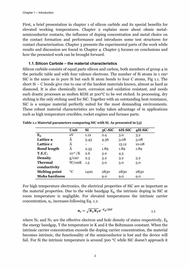
For correct measurements, the TLM structures have to be isolated from each other on the wafer, both laterally and vertically. In samples with epitaxial layers, the vertical isolation is the epitaxial interface below. For lateral isolation, mesa structures, etched down to the underlying epitaxial layer, are needed. The models behind the TLM structure assume a lateral current flow from one contact to the next. In addition to the mesa isolation, this also requires a minimal difference in the contact and mesa widths, Z and W, Fig 2.5 a). As illustrated in Fig 2.5 b) where W>Z, the current flow is no longer just linear and the sides of the contacts will also be involved in the current transport. A larger part of the contact than LT will be active in the current transport if W>Z which leads to an underestimated value of ρc and the contact performance.
Drawbacks of TLM measurements include the indirect measurement of the specific contact resistivity calculated from the RT measurements, at least three measurements are needed for one data point and five is a common standard, and at least two mask steps are needed: isolation of the mesa structures by etching and patterning of the metal contacts. The lower limit for TLM measurements is around 10-6 Ωcm2 [10].
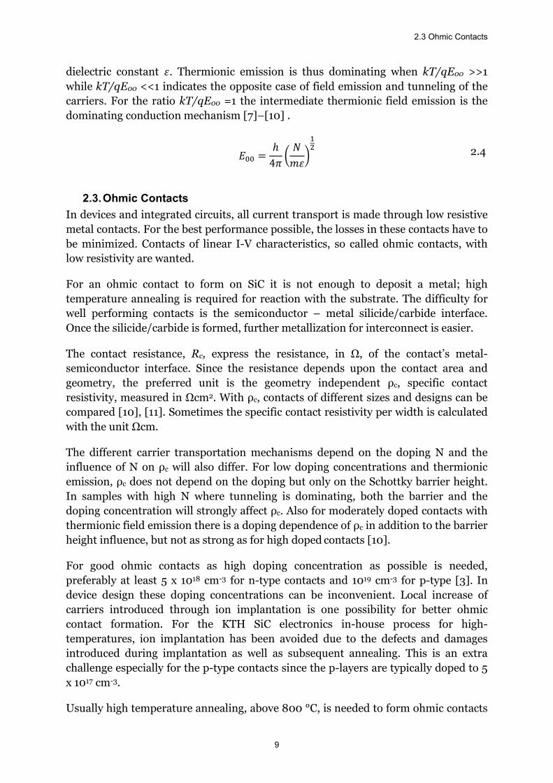
2.4.2. Cross-bridge Kelvin resistor structure Cross-bridge Kelvin resistor structures, CBKR, can be used for direct contact resistance measurements with a lower measuring limit. Here, the metal contact, center of Fig 2.6 a), is the only part of the structure where the voltage drop is measured and current flows. The resistance measured in a CBKR structure thus only originates from the contact. With a known contact size the specific contact resistivity can be calculated directly by multiplying with the area.
a) b)
Fig 2.5. a) A mesa width W close to the contact width Z gives lateral current flow while in b) with a mesa width W larger than the contact width Z, the current flow is no longer lateral and also the sides of the contacts are involved in the current transport.
2.5 Contact metallization
13
a)
b)
Fig 2.6 Schematic a) top view and b) side view of a Cross-bridge Kelvin resistor structure, CBKR with etched mesa (blue) and metallization (grey). The contact in common is seen in the middle (checkered).
Processing of CBKR structures requires at least four mask steps: mesa etch, patterning of passivation oxide and metallization pad patterning. Fig 2.6 b) shows what the isolated mesa structure might look like with the four contacts for measurements and the central contact for characterization. The passivation layer needed between the mesa and the top metallization is not shown in this drawing for clarity. The lower limit of the specific contact resistivity that can be estimated with this structure is around 10-8 Ωcm2 [3], [11], [13].
Table 2.1 Comparison of measurement techniques for ρc
Method Type Minimum number of mask steps Limit
TLM Indirect 2 mask steps: mesa etch, contact patterning 10-6 Ωcm2
Cross-bridge Kelvin resistor Direct
4 mask steps; mesa etch, contact patterning, contact
holes in oxide, top metallization 10-8 Ωcm2
2.5. Contact metallization Table 2.2 and Table 2.3 list examples from the literature of metals used for ohmic contacts to n- and p-type SiC respectively. Throughout the SiC history, numerous metals have been evaluated as candidates for contacts. The selection in the tables is connected to the metals evaluated within the work of this thesis.
To compare literature data of ohmic contact performance is difficult; both doping concentrations in the tested epitaxial layers and the choice of test structures will affect the specific contact resistivity. A general remark is that higher doping concentrations usually give better contacts. The few examples presented of ion implanted SiC show how a high, locally increased, doping concentration give impressively low specific contact resistivities.
As clearly seen in the tables, high annealing temperatures are needed for the ohmic contact formation. For n-SiC, the specific contact resistivity is generally lower than for p-SiC but good examples have been published also to p-SiC though mostly to very highly doped material.
Chapter 2 – Metal – Semiconductor contacts
14
2.5.1. Earlier work at KTH Nils Lundberg did in his thesis look into the use of cobalt silicides and tungsten carbides for Schottky contact and cobalt silicide for ohmic contacts to 6H-SiC. Experiments were made with contacts to epitaxial layers of both n- and p-doped 6H SiC. The cobalt contacts were evaporated while the tungsten contacts were deposited using chemical vapor deposition (CVD). Early experiments of ohmic contacts were measured with Kuphal structures [14] while after a comparison in [15], TLM structures were preferred.
Sang-Kwon Lee worked on titanium tungsten, and titanium carbide contacts for use on both n- and p-type 4H SiC. Samples of both epitaxial and implanted layers were tested.
2.5.2. Contacts in the in-house IC-process The contacts presently used in the SiC IC-process are Ni and Ni/Ti/Al for n- and p-doped SiC respectively. The Ni n-type contact form good ohmic contacts with contact resistivity around 10-6 Ωcm2. The Ni/Ti/Al has been a well performing contact for the low doping concentrations in the KTH SiC bipolar transistors [16][17].
2.5.3. CoSi2 as a silicide for ohmic contacts In the 1990’s Co was investigated for ohmic contacts to 6H-SiC in KTH with very good results regarding both n-type and p-type ohmic contacts. Unfortunately adhesion was a problem with stress occurring between the deposited film and the substrate making the films delaminate.
In the early work, different version of adding Si to the metallization was investigated. CoSi2 is a highly silicon consuming silicide, the ratio of consumed Si to added Co to form cobalt silicide is about 3.6:1. Since cobalt doesn’t form carbides, the use of Si results in a considerable release of C from the substrate. The presence of C in the interface can be detrimental for the contact formation and has to be minimized. By adding silicon during the metallization the silicidation can be performed with limited consumption of the substrate and release of carbon.
With thin, stacked layers, the high temperature annealing required for silicidation can be divided into different steps. The reaction temperature needed for deposited Si to react with Co is considerably lower than for the monocrystalline SiC substrate to react with Co. The approach used has been a lower temperature anneal for reaction between the sputtered layers of Si and Co followed by a high temperature anneal for final reaction with the substrate. Ideally the only silicide present after these anneals should be CoSi2.

2.5 Contact metallization
15
Table 2.2 Examples of metallizations reported for n-type ohmic contacts. Doping concentrations refers to epitaxial layer, implantation is marked by (impl).
N-type contacts Metal Deposition
(bottom/top) Polytype Doping
[cm-3] ρc
[Ωcm2] Anneal
[°C] Reference
Co 6H 7 x 10¹⁸ <3 x 10⁻⁵ 500 + 900 [15] 1995 Co/Si 6H 7 x 10¹⁸ <3 x 10⁻⁵ 500 + 900 [15]1995 Co/Si 6H 1.4 x 10¹⁹ <3 x 10⁻⁵ 500 + 900 [15]1995
Co/Si/Co/Si/Co 4H 1.1 x 10¹⁹ 1.8 x 10⁻⁶ 500 + 800 [18] 2004 Co/Si/Co 4H 1.1 x 10¹⁹ 1.5 x 10⁻⁶ 550 + 800 [19] 2004 C/Co/Au 4H 2.8 x 10¹⁸ 2.3 x 10⁻⁶ 550 + 1050 [20]2011
Ni 4H
(impl) 1 x10¹⁹ 5 x 10¹⁹
1 x 10¹⁹ 1.1 x 10¹⁹
6.0 x 10⁻⁶
6.5 x 10⁻⁵
1.5 x 10⁻⁵ 7.5 x 10⁻⁶
1050 1000 1000 950
[21] 2001 [22] 2007 [23] 1997 [24] 2002
Ni/Si 4H 6H
1 x 10¹⁹
1.8 x 10¹⁸ 2.7 x 10⁻⁵
1-3 x 10⁻⁴ 950 950
[25] 1997 [25] 1997
Ni/Si/Ni 4H 1.1 x 10¹⁹ 1.4 x 10⁻⁵ 550 + 800 [19] 2004 Si/Ni 4H
6H 2 x 10¹⁹
1.5 x 10¹⁹ 1.9 x 10⁻⁶
6.9 x 10⁻⁴ 900 300
[26] 2002 [27] 2004
Ti 4H >1020 8 x 10⁻⁴ 950 [28] 2000
TiC 4H 1.3 x 10¹⁹ 4 x 10⁻⁵ 950 [28] 2000
Table 2.3 Example of metallizations reported for p-type ohmic contacts. Doping concentrations refers to epitaxial layer, implantation is marked by (impl).
P-type contacts Metal Deposition
(bottom/top) Polytype Doping
[cm-3] ρc
[Ωcm2] Anneal [°C] Reference
Al/Ti 4H 4H
1 x 10¹⁹
7 x 10¹⁸ 6.4 x 10⁻⁴
1.5 x 10⁻⁴ 900 1000
[29] 1998 [30] 2000
Al/Ti/Al 4H 4.8 x 10¹⁸ 3.3 x 10⁻⁴ 1000 [31] 2004 [32] 2003
AlSi(2%)Ti(0.1%) 4H 3-5 x 10¹⁹ 9.6 x 10⁻⁵ 950 [33] 2001 Al-Ti 4H, 6H 1.3 x 10¹⁹ 5 x 10⁻⁵
- 3 x 10⁻⁵ 1000 [34] 1997
[35] 2002 Co 6H 2 x 10¹⁹ 4 x 10⁻⁴ 500 + 900 [36] 1996 Co/Si 6H 2 x 10¹⁹ 4 x 10⁻⁶ 500 + 900 [36] 1996 Ni 4H 2 x 10²⁰ 7 x 10⁻³ 1000 [37] 2002 Ni/Ti/Al 4H 3.9 x 10¹⁸
4 x 10¹⁷
(impl) 6 x10¹⁹
6.6 x 10⁻⁵
1.9 x 10⁻³
1.3 x 10⁻⁴
800 800 800
[38] 2003 [39] 2008 [39] 2008
Ti 4H >1020
1.3 x 10¹⁹
1.3 x 10¹⁹
1.3 x 10¹⁹
8 x 10⁻⁴
3.4 x 10⁻⁴
7.7 x 10⁻⁴
2-4 x 10⁻⁵
950 -
950 800
[40] 2002 [28] 2000 [28] 2000 [34] 1997
Ti-Al Ti/Al
4H 4H
4.8 x 10¹⁸
3 x 10²⁰ 2.5 x 10⁻⁴
10-6 1000 1000
[31] 2004 [37] 2002
Chapter 2 – Metal – Semiconductor contacts
16
Lundberg et al. improved the contact resistivity from 1.5 x 10⁻³ Ωcm2 to 9.2 x 10⁻⁴ Ωcm2, both measured at 400K, by the addition of Si to the contacts. In the same contacts, an addition of Ti improved the adhesion but hindered the silicide formation [14]. Cobalt contacts measured by TLM structures, [15], showed contact resistivity <3 x 10⁻⁵ Ωcm2 measured from 25 °C to 500 °C. Also to p-type 6H-SiC were ohmic cobalt silicide contacts with silicon addition (Si/Co/SiC) superior over Co/SiC-contacts resulting in the impressive specific contact resistivity <4 x 10⁻⁶ Ωcm2 [36]. Measurements at temperatures up to 200 °C increased the specific contact resistivity and ageing in furnace affected both the film morphology and the contact performance.
A few results regarding cobalt silicide contacts made to n-type 4H-SiC have been found in the literature. Cho et al., [18], made cobalt silicide contacts to 4H-SiC with an n-doped epitaxial layer. Their best result, 1.8 x 10⁻⁶ Ωcm2, was obtained from a multilayered contact (Co/Si/Co/Si/Co) annealed in a two-step process at 500 °C and 800 °C. With only a long time anneal at 800 °C, the contact resistivity was a decade lower and oxide was found in the contact. XRD measurements of the samples indicated CoSi and CoSi2 in both samples but in the best performing contacts, the CoSi2 phase was more dominating and no oxide present.
Yang et al., [19], compared layered Co/Si/Co contacts to Ni/Si/Ni contacts, both made to n-type 4H-SiC and characterized by TLM-structures. The cobalt contacts had ten times lower specific contact resistivity compared to the layered nickel contacts. For both contacts, the XRD spectra indicate the presence of several silicides; CoSi and CoSi2 for the cobalt contacts and NiSi and NiSi2 for the nickel contacts.
Introduction of C has also been reported, [20], where the contacts after anneal at 550 °C and 1050 °C resulted in contact resistivity of 2.3 x 10⁻⁶ Ωcm2. The contacts were also tested after 20 h at increasing temperatures up to 500 °C with stable results that are partly attributed the cobalt contact formation, partly the capping Au-layer preventing oxide formation.

17
3. Chapter 3 – Experimental Three types of contact metallizations have been made within this work. The novelty regarding the metallizations is first the design of a TLM structure with extended measurement pads; in the earlier work on ohmic contacts at KTH the contacts have been probed directly on the contacts. With the extended pads the characterization is more straightforward and the processing closer to the integrated circuit processing. Secondly, the sputter deposition technique used for the cobalt contacts opened up the possibility of layered contacts with very thin layers. Thirdly, the choice of epitaxial layers over implantation is also worth pointing out. The objective here was not solely to make ohmic contact to n- and p-doped SiC but also to meet the specific requirements of doping concentrations set by the KTH SiC integrated circuit and device design.
In this chapter the experimental part of the thesis work will be presented including the different types of wafers and epitaxial layers, comparison of the three mask sets, overview of the process flow and description of the experimental work in Paper I and II.
3.1. Wafers and epitaxial layers of the samples Three different types of samples have been fabricated and used referred to as TLM, Schottky and substrate chips, Table 3.1. All wafers have been n-type 4H SiC 4° off-axis and processed on the silicon face (0001).
Table 3.1 Epitaxial layers in processed wafers and chips.
Wafer Wafer size [mm]
Chip size [mm]
Epitaxial layers (from top, cm-3)
TLM Wafer 1 75 mm 12 x 12 mm 1 µm ND = 1.2 x 10¹⁹ 0.9 µm NA = 7 x 10¹⁷
TLM Wafer 2 100 mm 10 x 10 mm 1 µm ND = 1 x 10¹⁹ 1 µm NA = 1 x 10¹⁸
0.5 µm ND = 2 x 10¹⁸ Substrate 100 mm 10 x 10 mm No epitaxial layers

Chapter 3 – Experimental
18
The contact tests are investigated for future use in the in-house integrated circuit process and the epitaxial layers of the TLM wafers have been designed to correspond with the doping levels of the circuit wafers’ epitaxial layers. In the circuit wafers, contact metallization is made for emitter, base and collector layers with n, p and n-type doping respectively. Typical values for the n-doping is 1 x 1019 cm-3 while the p-type base is considerably lower, 5 x 1017 cm-3. The TLM wafers have thus had both high-doped n-layers and low-doped p-layers, further presented in the processing description, 3.3.
However, the epitaxial layers of the TLM wafers were not measured and are stated with their nominal values. Measurements of other SiC wafers have shown variations in both thicknesses doping concentration of the epitaxial layers over the surface. A difference between the thickness and doping concentrations ordered and the actual thickness/doping grown have also been seen.
RTA-tests, blanket metallization and process tests such as etch and deposition rate test were made on substrate chips; research grade substrate wafers without epitaxial layers. The substrate chips had an n-type doping concentration around 1019 cm-3, were cut to the same size as the TLM chips and included in the metallization runs together with the TLM chips.
3.2. Mask sets The three mask sets, designed and used in this work, will here be briefly introduced.
3.2.1. Mask sets for TLM structures Mask set “TLM 1” and “TLM 2” are for ohmic contact characterization using TLM structures including both n- and p-type mesas on the same chip. The first mask set was made for 12 x 12 mm chips on a 3 inch wafer. When changing from 3 inch to 100 mm wafers, a new mask set was required and at the same time improvements were made. In the second mask set, a top metallization for extended probing pads was introduced which made an oxide passivation step necessary to include in the process. At the same time, the chip size was adjusted to 10 x 10 mm.
With the top metallization layer, the contact size could be decreased from 100 x 200 µm2 to 50 x 100 µm2 while the extended pads, two to each contact, made probing easy and wire bonding possible, Fig 3.1.
The mesa width is 104 µm leaving a 2 µm alignment margin on each side after contact formation. The via openings are 30 x 30 µm2, two for each contact with 10 µm margin to the edges and 20 µm between the two via openings. The top metallization is 40 µm wide to cover the entire via openings and extends 45 µm over the contact leaving 10 µm margin on the top of the structure. For the n-mesas which are etched in two steps, the underlying mesa is 3 µm wider on each side, 110 µm in total.
In the processing, the contact metallization is made prior to the passivation oxide deposition. The contact size is larger than the via opening to minimize the risk of not

3.2 Mask sets
19
Fig 3.1 Drawing of TLM structure from mask set TLM 2 with the extended pads, and zoom-in of the mesa.
Fig 3.2 Schematic of via opening in the passivating oxide with the larger contact below and metallization on top.
covering the bottom of the via entirely. The top metallization is then larger than the via to verify that the via is entirely covered by metal, Fig 3.2.
3.2.2. Mask set for Schottky diodes The third mask set, “Schottky”, is a one-step metallization process intended for Schottky diodes of different sizes and shapes. The mask was made for chips and the pattern is divided vertically in the middle of the mask into two parts of similar pattern but opposite polarity, Fig 3.3, for metal patterning by either etching or lift-off techniques.
Fig 3.3 Part of the Schottky diode mask. The pattern is repeated over the entire mask with the left side (red) having opposite polarity from the right side (green).
The structures are squares, squares with rounded corners, circles, four-point stars and hexagons. The sizes are referred to as 50, 100, 200, 400 and 800 which are the sides of the square structures in µm. The structures of other geometries have identical areas as the squares. Hence, the structures can be evaluated either regarding size or
Chapter 3 – Experimental
20
shape. Each shape is present in all 5 sizes to check for influence of the area. For each size, the 5 different shapes makes investigation of the influence of the corners or the perimeter versus area possible.
The Schottky mask has mainly been used for patterning of substrate chips used for processing tests such as the RTA sequence development presented in 3.6.2.
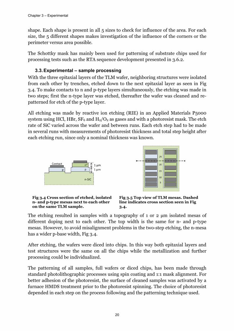
3.3. Experimental – sample processing With the three epitaxial layers of the TLM wafer, neighboring structures were isolated from each other by trenches, etched down to the next epitaxial layer as seen in Fig 3.4. To make contacts to n and p-type layers simultaneously, the etching was made in two steps; first the n-type layer was etched, thereafter the wafer was cleaned and re-patterned for etch of the p-type layer.
All etching was made by reactive ion etching (RIE) in an Applied Materials P5000 system using HCl, HBr, SF6 and H2/O2 as gases and with a photoresist mask. The etch rate of SiC varied across the wafer and between runs. Each etch step had to be made in several runs with measurements of photoresist thickness and total step height after each etching run, since only a nominal thickness was known.
Fig 3.4 Cross section of etched, isolated n- and p-type mesas next to each other on the same TLM sample.
Fig 3.5 Top view of TLM mesas. Dashed line indicates cross section seen in Fig 3.4.
The etching resulted in samples with a topography of 1 or 2 µm isolated mesas of different doping next to each other. The top width is the same for n- and p-type mesas. However, to avoid misalignment problems in the two-step etching, the n-mesa has a wider p-base width, Fig 3.4.
After etching, the wafers were diced into chips. In this way both epitaxial layers and test structures were the same on all the chips while the metallization and further processing could be individualized.
The patterning of all samples, full wafers or diced chips, has been made through standard photolithographic processes using spin coating and 1:1 mask alignment. For better adhesion of the photoresist, the surface of cleaned samples was activated by a furnace HMDS treatment prior to the photoresist spinning. The choice of photoresist depended in each step on the process following and the patterning technique used.

3.4 Electrical measurements – 2 or 4 probe techniques
21
For removal of any remaining monolayer of the photoresist in the pattern openings, the samples were plasma ashed in oxygen plasma prior to metallization.
The metal deposition techniques used are e-beam evaporation and sputtering. Materials evaporated within this work include Ni for n-type contacts and a stack of Ni/Ti/Al for p-type contacts. Co and Si were instead sputter deposited.
Contact annealing was made using RTA in N2 or Ar-flow at temperatures of 600-950 °C for 1-4 min depending on material
with the chip placed on a carrier Si wafer.
The measurements pads required a passivation layer which was achieved by PECVD deposited SiO2. On top of the oxide, a 1 µm Al top metallization layer was sputter deposited with a thin TiW or Ti/TiW adhesion layer below. The top metallization was wet etched with a photoresist mask.
3.4. Electrical measurements – 2 or 4 probe techniques Electrical measurements have been made on three probe stations depending on temperature – a semi manual probe station for measurements at -40 °C – 200 °C, probing on a hot chuck for measurements from ambient to 500 °C and when needed on a manual probe station capable of ambient up to 300°C. In the manual and semi manual probe stations the samples are in a closed chamber under dry air to minimize condensation. The hot chuck has the samples open in air. No measurements have been made under vacuum or inert gas.
The measurements have been made by a two- or four-probe setup, Fig 3.6, depending on the contact type measured. TLM-measurements of n-SiC typically have total resistances around 10-150 Ω. The resistance originating from cables and probes is comparable in a two-probe measurement of n-type, so all n-type contacts have been measured with a four-probe technique. On the other hand, TLM-measurements of p-type contacts to SiC have resistances at least a decade higher and the influence from the cables and probes is therefore negligible. No difference was seen between the two- and four-probe setups so all p-type contacts have been characterized by the two-probe setup.
Table 3.2 Process flow of the TLM chips.
TLM Processing step
TLM Mask Step N:o
Clean Etch of n-type epi 1 Photoresist removal Clean Etch of p-type epi 2 Photoresist removal Clean Sacrificial dry oxidation Dicing Clean Removal of sacrificial oxide Clean Metal deposition, patterned by lift-off 3 Lift-off and resist removal Anneal Oxide deposition and dry etch 4 Photoresist removal Top metal deposition and wet etch 5 Photoresist removal
Characterization

Chapter 3 – Experimental
22
Fig 3.6 Schematic of two and four probe I-V measurement.
The temperatures reported are the set points of the respective chuck, the actual temperature of the sample was measured to differ 8-10 °C below the set point at 400 °C and 500 °C and not more than 5 °C for lower temperatures.
3.5. Experimental work in Paper I In Paper I, TLM chips with Ni n-type contacts, Ni/Ti/Al p-type contacts and Al top metallization were processed and compared to samples with the same metals from the bipolar IC batch published in [41]. In Paper I the two sample types are referred to as “test chips”, Fig 3.7, and “circuit chips”, Fig 3.8.
Though all contacts were characterized by TLM structures with contact sizes 50 x 100 µm, the epitaxial layers and processing were differing. The TLM structures of the test chips also included the 200 x 200 µm measurement pads while the circuit chips were probed directly on the TLM contacts. Electrical characterization of the samples was made by probing, as described in 3.4, in the temperature interval -40 °C – 500 °C.
3.5.1. “TLM samples” Paper I The test chips were TLM chips from wafer 2 patterned with the TLM 2 mask set and etched as earlier described to form the n- and p-type mesas. The processing partly followed the in-house IC process. Ni- and Ni/Ti/Al for n- and p-type contacts respectively, were evaporated in two separate steps and patterned by lift-off technique. Ni, deposited first, was annealed for 1 min at 950 °C, while the later deposited Ni/Ti/Al contact was annealed for 1 minute at 815 C. After the contact formation, 550 nm PECVD SiO2 was deposited for isolation. The last step included the sputter deposition of the top metallization Al with a Ti/TiW adhesion layer below. The measurement pads were patterned by etching of the top metal.
3.5.2. “Circuit samples“ Paper I The circuit chips also measured in Paper I had been made following the IC process where the passivation oxide is deposited prior to the metal deposition and formation. The Al top metallization was also the interconnecting metallization in the circuits and gave a top coating on the TLM contacts. Anneal temperatures and metal thicknesses are similar, but doping is slightly different. Details of the circuit chip processing are found in [17], [41].
3.6 Experimental work in Paper II
23
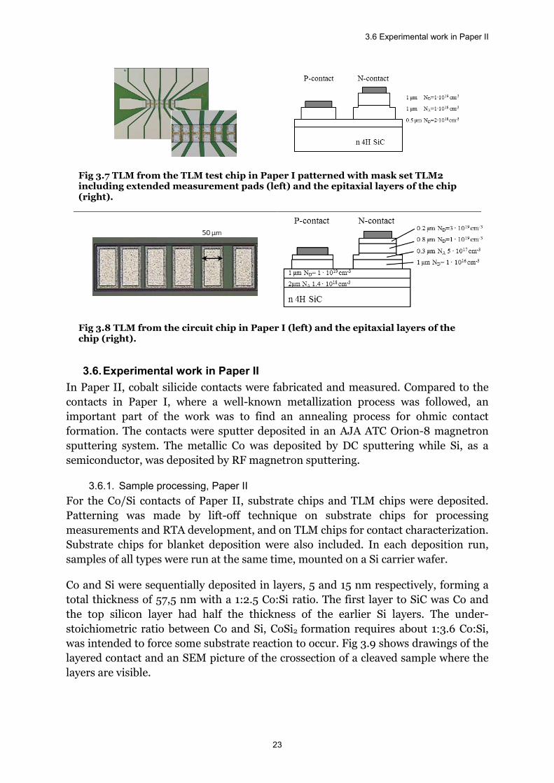
3.6. Experimental work in Paper II In Paper II, cobalt silicide contacts were fabricated and measured. Compared to the contacts in Paper I, where a well-known metallization process was followed, an important part of the work was to find an annealing process for ohmic contact formation. The contacts were sputter deposited in an AJA ATC Orion-8 magnetron sputtering system. The metallic Co was deposited by DC sputtering while Si, as a semiconductor, was deposited by RF magnetron sputtering.
3.6.1. Sample processing, Paper II For the Co/Si contacts of Paper II, substrate chips and TLM chips were deposited. Patterning was made by lift-off technique on substrate chips for processing measurements and RTA development, and on TLM chips for contact characterization. Substrate chips for blanket deposition were also included. In each deposition run, samples of all types were run at the same time, mounted on a Si carrier wafer.
Co and Si were sequentially deposited in layers, 5 and 15 nm respectively, forming a total thickness of 57,5 nm with a 1:2.5 Co:Si ratio. The first layer to SiC was Co and the top silicon layer had half the thickness of the earlier Si layers. The under-stoichiometric ratio between Co and Si, CoSi2 formation requires about 1:3.6 Co:Si, was intended to force some substrate reaction to occur. Fig 3.9 shows drawings of the layered contact and an SEM picture of the crossection of a cleaved sample where the layers are visible.
Fig 3.7 TLM from the TLM test chip in Paper I patterned with mask set TLM2 including extended measurement pads (left) and the epitaxial layers of the chip (right).
Fig 3.8 TLM from the circuit chip in Paper I (left) and the epitaxial layers of the chip (right).

Chapter 3 – Experimental
24
Fig 3.9 Schematic of the layered CoSi2 contacts to n- and p-SiC mesas (left and middle) and scanning electron microscopy image of a cleaved sample showing the layers (right).
After an RTA process was established, see below, the continued TLM chip processing followed the one in Paper I with deposition of a passivating PECVD oxide layer and a sputter deposited Al top metallization patterned by wet etching. The sputter system used for Al was a different one and only TiW was used as an adhesion layer. Though well working, the top metallization looked much rougher than the samples in Paper I, Fig 3.10.
Fig 3.10 Co/Si sample with rough Al top metallization.
In Paper II sample A and B are presented were A is such a substrate test chip and B a TLM chip annealed with a process chosen from the results of sample A.
3.6.2. RTA development For the Co/Si samples, an RTA sequence had to be developed. From literature a two-step anneal was chosen. Several substrate chips were included in each Co/Si deposition run. By using the Schottky mask for patterning, the samples could be probed. Two types of I-V measurements were made as depicted in Fig 3.11; a two-probe measurement between adjacent contacts and with the two probes on diagonal corners of a larger contact. The addition of the measurement on the same contact was in order to see how the layered contact behaved upon RTA treatments.
Fig 3.11 Probing for RTA development a) between two contacts and b) with two probes on the same contact.
3.6 Experimental work in Paper II
25
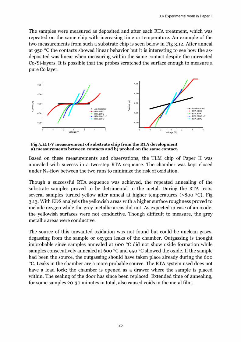
The samples were measured as deposited and after each RTA treatment, which was repeated on the same chip with increasing time or temperature. An example of the two measurements from such a substrate chip is seen below in Fig 3.12. After anneal at 950 °C the contacts showed linear behavior but it is interesting to see how the as-deposited was linear when measuring within the same contact despite the unreacted Co/Si-layers. It is possible that the probes scratched the surface enough to measure a pure Co layer.
-6 -4 -2 0 2 4 6
-0,08
-0,04
0,00
0,04
0,08
As-deposited RTA 600C RTA 800C RTA 800C x 3 RTA 950C
Cur
rent
[A]
Voltage [V] -6 -4 -2 0 2 4 6
-0,08
-0,04
0,00
0,04
0,08
Cur
rent
[A]
Voltage [V]
As-deposited RTA 600C RTA 800C RTA 800C x 3 RTA 950C
Fig 3.12 I-V measurement of substrate chip from the RTA development a) measurements between contacts and b) probed on the same contact.
Based on these measurements and observations, the TLM chip of Paper II was annealed with success in a two-step RTA sequence. The chamber was kept closed under N2-flow between the two runs to minimize the risk of oxidation.
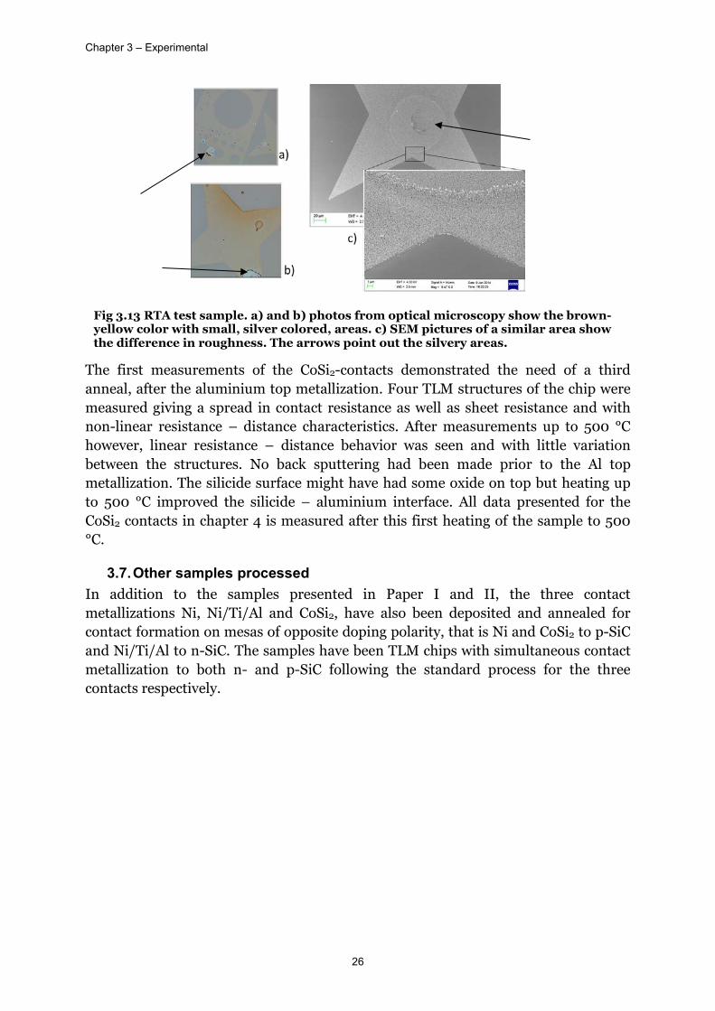
Though a successful RTA sequence was achieved, the repeated annealing of the substrate samples proved to be detrimental to the metal. During the RTA tests, several samples turned yellow after anneal at higher temperatures (>800 °C), Fig 3.13. With EDS analysis the yellowish areas with a higher surface roughness proved to include oxygen while the grey metallic areas did not. As expected in case of an oxide, the yellowish surfaces were not conductive. Though difficult to measure, the grey metallic areas were conductive.
The source of this unwanted oxidation was not found but could be unclean gases, degassing from the sample or oxygen leaks of the chamber. Outgassing is thought improbable since samples annealed at 600 °C did not show oxide formation while samples consecutively annealed at 600 °C and 950 °C showed the oxide. If the sample had been the source, the outgassing should have taken place already during the 600 °C. Leaks in the chamber are a more probable source. The RTA system used does not have a load lock; the chamber is opened as a drawer where the sample is placed within. The sealing of the door has since been replaced. Extended time of annealing, for some samples 20-30 minutes in total, also caused voids in the metal film.
Chapter 3 – Experimental
26
Fig 3.13 RTA test sample. a) and b) photos from optical microscopy show the brown-yellow color with small, silver colored, areas. c) SEM pictures of a similar area show the difference in roughness. The arrows point out the silvery areas.
The first measurements of the CoSi2-contacts demonstrated the need of a third anneal, after the aluminium top metallization. Four TLM structures of the chip were measured giving a spread in contact resistance as well as sheet resistance and with non-linear resistance – distance characteristics. After measurements up to 500 °C however, linear resistance – distance behavior was seen and with little variation between the structures. No back sputtering had been made prior to the Al top metallization. The silicide surface might have had some oxide on top but heating up to 500 °C improved the silicide – aluminium interface. All data presented for the CoSi2 contacts in chapter 4 is measured after this first heating of the sample to 500 °C.
3.7. Other samples processed In addition to the samples presented in Paper I and II, the three contact metallizations Ni, Ni/Ti/Al and CoSi2, have also been deposited and annealed for contact formation on mesas of opposite doping polarity, that is Ni and CoSi2 to p-SiC and Ni/Ti/Al to n-SiC. The samples have been TLM chips with simultaneous contact metallization to both n- and p-SiC following the standard process for the three contacts respectively.

27
4. Chapter 4 – Results and Discussion In this chapter the results presented in Paper I and II will be discussed and compared as well as non-published results of a common contact metallization for n- and p-SiC.
4.1. Ni and Ni/Ti/Al contacts at elevated temperatures Paper I, “Characterization of Ohmic Ni/Ti/Al and Ni Contacts to 4H-SiC from -40°C to 500°C”, focuses on the contacts used in the KTH in-house SiC IC-process and their characteristics at extreme temperatures. Though Ni n-contacts are widely reported also at elevated temperatures, other reports of the Ni/Ti/Al p-contacts for this vast temperature range has not been found elsewhere. For work within this ohmic contact project, Paper I is of interest for the continued work and analysis of future results. The performance of the TLM contact test chips have been compared to the IC chips including the variation of the epitaxial layers and processing differences. In Fig 4.1 the specific contact resistivities and sheet resistances are presented against temperature in °C. For better comparison, the axes for the n- and p-type contacts are the same for ρc and Rsh respectively. The measurements have been plotted against 1/T [K-1] in Fig 4.2, for better clarity regarding the temperature dependence and for extracting activation energy.
4.2. CoSi2 at elevated temperatures The measurements of the Co/Si contacts presented in Paper II, “Sputtered Ohmic Cobalt Silicide Contacts to 4H-SiC” are plotted in Fig 4.3 versus 1/T [K-1] and with the same axes as in Fig 4.2.
The electrical behavior of the CoSi2 contacts showed a steep decrease in specific contact resistivity from -40 °C up to 200 °C. For temperatures from 200 °C and above, little difference is seen for the specific contact resistivity. The sheet resistance on the other hand has a minimum for 100 – 200 °C above which increasing temperatures increases the sheet resistance.

Chapter 4 – Results and Discussion
28
-100 0 100 200 300 400 500101
102
103
104
105
106
-100 0 100 200 300 400 50010-6
10-5
10-4
10-3
10-2
-100 0 100 200 300 400 50010-6
10-5
10-4
10-3
10-2
-100 0 100 200 300 400 500101
102
103
104
105
106
IC TLM
b)
d)
a)
ρ C [Ω
cm2 ]
ρ C [Ω
cm2 ]
TLM IC
c)
T [oC]
Ni n-contact
RS
H [Ω
/sq]
RS
H [Ω
/sq]
T [oC]
Ni/Ti/Al p-contact
T [oC]
T [oC]
Fig 4.1 Logarithmic specific contact resistivity ρc and sheet resistance Rsh vs T of the Ni n-contacts, left, and Ni/Ti/Al p-contacts, right.
0,002 0,003 0,00410-6
10-5
10-4
10-3
10-2
0,002 0,003 0,004
102
103
104
105
0,002 0,003 0,004
102
103
104
105
0,002 0,003 0,00410-6
10-5
10-4
10-3
10-2
ρ C [Ω
cm2 ]
ρ C [Ω
cm2 ]
Ni n-contact
RS
H [Ω
/sq]
IC TLM
Ni/Ti/Al p-contact
1/T [K] 1/T [K]
1/T [K]
IC TLM
RS
H [Ω
/sq]
1/T [K]
T [oC]
500 400 300 200 100 0
b)
c) d)
T [oC]
T [oC]
a)
500 400 300 200 100 0
500 400 300 200 100 0T [oC]
500 400 300 200 100 0
Fig 4.2 Logarithmic specific contact resistivity ρc and sheet resistance Rsh versus 1/T of the Ni n-contacts, left, and Ni/Ti/Al p-contacts, right.

4.2 CoSi2 at elevated temperatures
29
0,002 0,003 0,00410-7
10-6
10-5
10-4
10-3
10-2
10-1
0,002 0,003 0,004101
102
103
104
105
106
ρ c [Ω
cm2 ]
1/T [K-1]
500400 300 200 100 0T [oC]
Rsh
[Ω/s
q]
1/T [K-1]
500400 300 200 100 0T [oC]
Fig 4.3 Measurements of CoSi2 contacts at T = -40 °C – 500 °C, a) specific contact resistivity ρc and b) sheet resistance Rsh.
0,002 0,003 0,004
10-5
10-4
0,002 0,003 0,004102
1,5x10²
2x10²
Rsh
[Ω/s
q]
a)
ρ c [Ω
cm2 ]
1/T [K-1]
b)
1/T [K-1]
CoSi Ni
500400 300 200 100 0T [oC]
500400 300 200 100 0T [oC]
Fig 4.4 Co/Si and Ni contacts vs 1/T a) specific contact resistivity ρc and b) sheet resistance Rsh.
0,0025 0,0030 0,0035 0,0040 0,0045101
102
103
104
105
0,0025 0,0030 0,0035 0,0040 0,0045101
102
103
104
105
b)
Rsh
[Ω/s
q]
1/T [K-1]
CoSi Ni
a)
100 50 0 -50T [oC] T [oC]
1/T [K-1]
Ni/Ti/Al Slope for
Ea=100 meV
100 50 0 -50
Fig 4.5 Arrhenius plots for extraction of the dopant atoms activation energy Ea from the sheet resistance Rsh for a) Ni and CoSi2 and b) Ni/Ti/Al.
Chapter 4 – Results and Discussion
30
4.3. Comparison Ni vs CoSi2
4.3.1. Sheet resistance The Ni and CoSi2 chips were from the same wafer and the measurements are compared in Fig 4.4. The slight variation in sheet resistance between the samples might very well originate from doping concentration differences over the wafer. The temperature dependence, however, is corresponding well between the chips and to other work from KTH [42].
4.3.2. Activation energy of dopant atoms From the sheet resistance the activation energy of the dopant atoms can be extracted by plotting lnRsh vs 1/T where the activation energy Ea corresponds to the slope. As seen in Fig 4.2 c), d) and Fig 4.4 b), the slope varies depending on temperature and at least two physical phenomena are needed to explain the variation in the entire temperature interval. For temperatures up to 100 °C plots of the same measurements are therefore found in Fig 4.5 a) and b) for the n- and p-contact respectively. In the Ni/Ti/Al-plot, the calculated slope for Ea = 100 meV is added for comparison. The extracted activation energies are 11 meV for Ni, 12 meV for CoSi2 and 80 meV for Ni/Ti/Al contacts, all considerably lower than literature values. No conclusions can be drawn except that the n-type measurements have the same behavior irrespective of contact metal.
4.3.3. Temperature dependence of the transfer length The transfer length LT, subtracted from the x-intercept of the TLM graphs, has been plotted for the three contact metallizations in Fig 4.6. The contacts exhibit interesting behavior with respect to temperature. The large difference in doping concentration, 1 x 10¹⁸ for p-type versus 1 x 10¹⁹ on n-type, is not seen in the transfer length. Instead, here the measurements of Ni and Ni/Ti/Al, on n- and p-type respectively, show very close values of LT. This implies that there is a relationship in the decrease of the specific contact resistivity and sheet resistance with increased doping concentration, which was earlier expressed in Eq. 2.5 as LT=√(ρc/Rsh). Overall, the transfer length is decreasing with temperature in the measurements; the sheet resistance increase is thus dominating over the decrease in specific contact resistivity.
On the other hand, the transfer length of the CoSi2 contact, n-type, show a very different behavior. For temperatures below 200 °C, LT greatly increases with decreasing temperature. It signifies a larger influence from the contact resistivity on LT than from the sheet resistance.
With the comparison of the sheet resistance from the CoSi2 and Ni measurements, both made on n-type mesas on chips from the same wafer, the strong temperature dependence is thus only from the specific contact resistivity, not from the sheet resistance.

4.3 Comparison Ni vs CoSi2
31
LT also gives important data regarding the contact sizing. According to the TLM theory, the contact length L has to be >1.5 LT. The smallest contacts in the KTH SiC IC design are 4 x 4 µm2 which, according to the measurements above, is enough for the n-type Ni contacts regardless of temperature and for the Ni/Ti/Al contacts from room temperature and above. With the concerns about the temperature dependence of the CoSi2 contacts, improvement of the contact formation should be made before making conclusions regarding the LT, and thus acceptable values of L.
4.3.4. Measurements before and after high temperature The contacts’ responses to extreme temperatures can be characterized by measurements at 25 °C before, in between and after, the extreme temperature measurements up to 500 °C. No degradation of the contact should be seen in this type of measurement.
A slight decrease in the Ni/Ti/Al contact can be seen in Fig 4.7 while the jump of the specific contact resistivity for the Ni-contacts after 500 °C is more pronounced. The CoSi2 contacts did not only show stability after elevated temperatures but even a slight improvement after the harsh treatment of measurements with the chip at 300 – 500 °C for several hours.
4.3.5. Comparison with literature data The n-type contacts made in this work, Ni and CoSi2, are in Fig 4.8 presented together with the literature results of the CoSi2 contacts of [15], [18], [19].
The very low contact resistivities presented in [15] and [16], Cho and Yang in the figure, are debatable. Their contacts were characterized by linear TLM structures on epitaxial n-SiC but the experimental description of the samples does not include mesa isolation etch. The risk of an underestimation of the measured total resistance used for the specific contact resistivity calculations can not be excluded.
The Lundberg contacts, [15], showed little variation when measured at different temperatures. The contact resistance was not as good as the contacts of Paper II, but it has to be remembered that these contacts were to 6H-SiC.
0 200 400 6000
1
2
3
4
5
6
7
8L T [
µm]
T [oC]
CoSi Ni/Ti/Al Ni
Before HT After 200 C After 500 C10-7
10-6
10-5
10-4
10-3
10-2
10-1
NiTiAl CoSi Ni
ρ c [Ω
cm2 ]
Fig 4.6 Transfer length LT measured and calculated at temperatures -40 - 500 °C
Fig 4.7 Specific contact resistivity ρc at 25 °C before and after heating.

Chapter 4 – Results and Discussion
32
Taking the earlier presented results of the Paper II CoSi2 contacts into account regarding the temperature behavior of ρc, Rsh and at 25 °C; the ρc at elevated temperatures, 200-500 °C, seem to be more accurate to compare in Fig 4.8. Within this temperature range, the Paper II CoSi2 contacts are not only superior to the Lundberg contacts but also approach the performance of the currently used Ni contacts. Improved contact processing is necessary including characterization of the entire temperature range before final conclusions can be drawn. However, the contact performance of the CoSi2 contacts is good.
4.4. A combined n- and p-type contact? Since bulk SiC is n-type, p-type contacts could not be tested on substrate chips. The TLM chips however had mesas of both doping polarities. Some samples have been patterned for n- and p-type mesas simultaneously which has enabled tests of the metallization on both polarities.
Neither Ni nor Ni/Ti/Al, the choice at KTH for n- and p-type contacts respectively, gave ohmic contacts when measured on the opposite type of doping. Fig 4.9 a) includes Ni, CoSi2 and Ni/Ti/Al contacts on n-SiC. The non-ohmic behavior of the Ni/Ti/Al, 5 µm spacing in a p-TLM structure with contacts sized 50 x 100 µm2, is clearly seen as a flat curve with barriers. To p-SiC on the other hand, the opposite behavior is seen for the three metallizations in Fig 4.9 b). The Ni, 20 µm spacing on TLM structure with contacts sized 100 x 200 µm2, exhibit clear barriers. For CoSi2 contacts to p-SiC, two curves are included with totally different behavior.
0,002 0,003 0,00410-6
10-5
10-4
10-3
10-2
ρ c [Ω
cm2 ]
1/T [K]
CoSi N. Lundberg - n-type 6H-SiC CoSi Paper II Ni Paper I CoSi Cho CoSi Yang n-type 4H-SiC
500 400 300 200 100 0
T [oC]
Fig 4.8 Specific contact resistivity ρc of CoSi2 contacts compared to literature ([15], [18] [19]) and Ni contacts in Paper I, all to n-SiC.

4.4 A combined n- and p-type contact?
33
The CoSi2 contacts were ohmic to n-SiC after anneal as presented in Paper II and discussed in Chapter 3.6.2. To p-SiC, CoSi2 contacts were measured on TLM structures with 50 x 100 µm2 contacts. The non-symmetric behavior, seen in Fig 4.10, indicates there might be an oxide present in the interface. High voltages were applied to break any such oxide. A voltage sweep of ±50V did not affect the behavior though ±75 V broke the barrier in some measurements and ±200 V was needed for others. In Fig 4.10 a), contacts with the spacing 20 µm have been measured. The almost linear measurement, ±0.01 A, has a total resistance varying between 650-2200 Ω. As a comparison, the Ni/Ti/Al contacts, spacing 20 µm and measured at 25 °C, had a total resistance just below 3000 Ω. The two CoSi2 curves in Fig 4.9 b) are the same as in Fig 4.10.
The results were not consistent. In other p-contacts of the chip, the ±75 V voltage sweep resulted in lower resistance but the curve remained non-symmetric. Sweeps of
-25 -20 -15 -10 -5 0 5 10 15 20 25
-1,0x10⁻³
-5,0x10⁻⁴
0,0
5,0x10⁻⁴
1,0x10⁻³
-3 -2 -1 0 1 2 3
-1,0x10⁻³
-5,0x10⁻⁴
0,0
5,0x10⁻⁴
1,0x10⁻³
Ni/Ti/Al Ni CoSi CoSi
Voltage [V]
p-SiC
b)
Cur
rent
[A]
a)
Ni/Ti/Al Ni CoSi
Voltage [V]
n-SIC
Fig 4.9 I-V curves of Ni, CoSi2 and Ni/Ti/Al contacts to a) n-SiC and b) p-SiC. See Fig 4.10 regarding the two CoSi2 curves.
-80 -60 -40 -20 0 20 40 60 80
-1,0x10⁻²
-5,0x10⁻³
0,0
5,0x10⁻³
1,0x10⁻²
Cur
rent
[A]
Voltage [V]
1) +/- 50 V2) +/- 75 V3) +/- 0.01 A
-20 -10 0 10 20
-5,0x10⁻³
0,0
5,0x10⁻³
Cur
rent
[A]
Voltage [V]
5 10 15 20 25
Fig 4.10 I-V curves of CoSi2 contact to p-SiC (as in Fig 4.9) before and after high voltage sweep.
Fig 4.11 TLM measurement of CoSi2 contacts to p-SiC after ±200V sweep with spacing 5, 10, 15, 20, 25 µm.

Chapter 4 – Results and Discussion
34
±200 V did sometime give almost linear I-V curves, sometimes strongly non-symmetric I-V curves.
An attempt of a TLM measurement of the p-type CoSi2 contacts is presented in Fig 4.11 where all measurements were made after sweeps of ±200 V. As clearly seen, large difference in linearity exist between the measurements. Increase in spacing between the contacts have however an impact on the measurement with larger resistance for larger spacing.
If the behavior of the CoSi2 contacts to p-SiC originate from interface oxide, the origin has to be found. With the oxide formation seen during the RTA tests, the annealing is a probable source. The contacts to p-SiC were made on the same chip as the Paper II n-SiC contacts. Even if the n-type CoSi2 contacts showed ohmic characteristics, an improved anneal with exclusion of interfacial oxide could also improve the n-contacts specific contact resistivity.

35
5. Chapter 5 – Conclusions and Future work This chapter includes conclusions from the results in chapter 4 and suggestions how the results could be brought forward in future work.
5.1. Conclusions Out of the tested contacts, the currently used Ni was the best n-contact and Ni/Ti/Al the best p-contact. Neither of the two gave ohmic contacts when measured to TLM structures of the opposite doping polarity. Even if a process was found to form for example Ni/Ti/Al ohmic contacts to n-SiC with an altered annealing temperature, two different annealing temperatures would require two separate metal deposition steps and the benefits of a common metallization would be lost.
The CoSi2 contacts were ohmic to n-SiC and exhibited specific contact resistivity ρc in the lower 10-5 Ωcm2 range at room temperature. Nevertheless, the comparison of the CoSi2 contacts to Ni contacts resulted in several arguments of an incomplete contact formation or interfacial oxide present in the CoSi2 contacts.
To p-SiC was a non-linear I-V curve without barriers measured for the CoSi2 contacts after sweeps of higher voltages. Although the total resistances RT varied, the lower RT was less than 25% of the Ni/Ti/Al p-type contacts and the maximum RT was still about the same as for Ni/Ti/Al-contacts.
With an incomplete contact formation and/or presence of an interfacial oxide, improvements of the CoSi2 contact processing might give both better n-contacts and result in ohmic p-contacts.
The CoSi2 n-type contacts did show good results at elevated temperatures. In combination with the promising results on p-SiC, CoSi2 can be a candidate for a common contact metallization to n- and p-type 4H SiC.
Chapter 5 – Conclusions and Future work
36
5.2. Future work Layered contacts could be further investigated for optimization of the Si-metal ratio in addition to an optimized RTA sequence. In addition to the Si-metal ratio it would also be of interest to test whether Si or metal should be deposited first to SiC.
For P-contact metallization, tests on p-type SiC of higher doping concentrations would be interesting to do as pre-study and comparison for low-doped p-contacts.
The wafers used with epitaxial layers enabling TLM structures of both n- and p-SiC on the same chip, have proven to be very useful, the sample makes measurements on the opposite polarity possible with equal metallization and annealing treatment.
As mentioned in chapter 3, cross-bridge Kelvin resistor structures have been discussed to be used in future mask sets in addition to TLM structures. The number of mask steps for CBKR structures would not exceed the number of mask steps used for the TLM with top metallization. In favor of CBKR is the direct measurement of the contact resistance. On the other hand, neither SiC material nor SiC processing is perfect and with only one measurement, material defects would not be visible in the same way as when five points are plotted against distance. The measurement range would also be increased.
Reliability tests have been a recurring question regarding the contacts. Though it would be of interest to see how the contacts react to ageing in a furnace both electrically and morphologic, real reliability tests would preferably be made on capped samples or at least wire bonded samples.

37
6. References [1] N. Lundberg, “Thermally Stable Electrical Contacts to 6H Silicon Carbide,” KTH Royal Institute
of Technology, 1996.
[2] S.-K. Lee, “Processing and Characterization of Silicon Carbide ( 6H- and 4H-SiC ) Contacts for High Power and High Temperature Device Applications,” KTH Royal Institute of Technology, 2002.
[3] C.-M. Zetterling, Ed., Process Technology for Silicon Carbide Devices. IET, 2002, p. 176.
[4] S. E. Saddow and A. Agarwal, Eds., Advances in Silicon Carbide Processing and Applications. Artech House, 2004, p. 228.
[5] W. J. Choyke and G. Pensl, “Physical Properties of SiC,” MRS Bull., vol. 22, no. 03, pp. 25–29, Mar. 1997.
[6] “Silicon Carbide Substrates and Epitaxy Product Specifications.” [Online]. Available: http://www.cree.com/~/media/Files/Cree/Chips and Material/Data Sheets Material/MATCATALOG.pdf. [Accessed: 09-Oct-2014].
[7] E. H. Rhoderick and R. H. Williams, Metal-semiconductor Contacts, Second edi. Oxford: Oxford University Press, 1988.
[8] C. Hu, Modern semiconductor devices for integrated circuits, 1st ed. Pearson, 2009, p. 384.
[9] D. K. Schroder, Semiconductor Material and Device Characterization, Second. Wiley-IEEE Press, 1998.
[10] F. Roccaforte, F. La Via, and V. Raineri, “Ohmic Contacts to SiC,” Int. J. High Speed Electron. Syst., vol. 15, no. 04, pp. 781–820, Dec. 2005.
[11] D. Schroder, Semiconductor material and device characterization, Third edit. 2006.
[12] L. Lanni, B. G. Malm, C.-M. Zetterling, and M. Östling, “A 4H-SiC Bipolar Technology for High-Temperature Integrated Circuits,” Journal of Microelectronics and Electronic Packaging, vol. 10, no. 4. pp. 155–162, 2013.
[13] S. J. Proctor and L. W. Linholm, “A direct measurement of interfacial contact resistance,” IEEE Electron Device Lett., vol. 3, no. 10, pp. 294–296, Oct. 1982.

References
38
[14] N. Lundberg and M. Östling, “Cobalt Silicide OHMIC Contacts to 6H-SiC,” MRS Proc., vol. 339, p. 229, Feb. 1994.
[15] N. Lundberg, M. Östling, Lundberg N., and Ostling M., “CoSi2 ohmic contacts to n-type 6H-SiC,” Solid. State. Electron., vol. 38, no. 12, pp. 2023–2028, 1995.
[16] R. Ghandi, M. Domeij, B. Buono, C.-M. Zetterling, and M. Ostling, “Fabrication of 2700-V 12-<formula formulatype=‘inline’><tex Notation=‘TeX’>$\hboxm\Omega \cdot \hboxcm^2$</tex> </formula> Non Ion-Implanted 4H-<emphasis emphasistype=‘roman’>SiC</emphasis> <emphasis emphasistype=‘roman’>BJTs </emphasis> With Common,” IEEE Electron Device Lett., vol. 29, no. 10, pp. 1135–1137, Oct. 2008.
[17] L. Lanni, R. Ghandi, B. G. Malm, C.-M. Zetterling, and M. Östling, “Design and characterization of high-temperature ECL-based bipolar integrated circuits in 4H-SiC,” … IEEE Trans., vol. 59, no. 4, pp. 1076–1083, 2012.
[18] N.-I. Cho, K.-H. Jung, and Y. Choi, “Improved ohmic contact to the n-type 4H-SiC semiconductor using cobalt silicides,” Semicond. Sci. Technol., vol. 19, no. 3, pp. 306–310, Mar. 2004.
[19] S. J. Yang, C. K. Kim, I. H. Noh, S. W. Jang, K. H. Jung, and N. I. Cho, “Study of Co- and Ni-based ohmic contacts to n-type 4H-SiC,” Diam. Relat. Mater., vol. 13, no. 4–8, pp. 1149–1153, Apr. 2004.
[20] Y. Wang, C. Liu, S. Gu, and C. Zhang, “Ohmic contact behaviour of Co/C/4H-SiC structures,” J. Semicond., vol. 32, no. 4, p. 044003, Apr. 2011.
[21] L. G. Fursin, J. H. Zhao, and M. Weiner, “Nickel ohmic contacts to p- and n-type 4H-SiC,” Electron. Lett., vol. 37, no. 17, p. 1092, 2001.
[22] H.-S. Lee, M. Domeij, C.-M. Zetterling, M. Ostling, F. Allerstam, and E. O. Sveinbjornsson, “1200-V 5.2-mOhm cm2 4H-SiC BJTs With a High Common-Emitter Current Gain,” IEEE Electron Device Lett., vol. 28, no. 11, pp. 1007–1009, Nov. 2007.
[23] C. Hallin, R. Yakimova, B. Pécz, A. Georgieva, T. Marinova, L. Kasamakova, R. Kakanakov, and E. Janzén, “Improved Ni ohmic contact on n-type 4H-SiC,” J. Electron. Mater., vol. 26, no. 3, pp. 119–122, Mar. 1997.
[24] S.-K. Lee, C.-M. Zetterling, and M. Östling, “Microscopic mapping of specific contact resistances and long-term reliability tests on 4H-silicon carbide using sputtered titanium tungsten contacts for high temperature device applications,” J. Appl. Phys., vol. 92, no. 1, p. 253, Jul. 2002.
[25] T. Marinova, A. Kakanakova-Georgieva, V. Krastev, R. Kakanakov, M. Neshev, L. Kassamakova, O. Noblanc, C. Arnodo, S. Cassette, C. Brylinski, B. Pecz, G. Radnoczi, and G. Vincze, “Nickel based ohmic contacts on SiC,” Mater. Sci. Eng. B, vol. 46, no. 1–3, pp. 223–226, Apr. 1997.
[26] T. Nakamura and M. Satoh, “NiSi2 ohmic contact to n-type 4H-SiC,” Mater. Sci. Forum, vol. 389–393, pp. 889–892, Apr. 2002.
[27] C. Deeb and A. H. Heuer, “A low-temperature route to thermodynamically stable ohmic contacts to n-type 6H-SiC,” Appl. Phys. Lett., vol. 84, no. 7, p. 1117, Feb. 2004.
[28] Lee S.-K., Zetterling C.-M., Ostling M., Palmquist J.-P., Hogberg H., and Jansson U., “Low resistivity ohmic titanium carbide contacts to n- and p-type 4H-silicon carbide,” Solid. State. Electron., vol. 44, no. 7, pp. 1179–1186, 2000.

5.2 Future work
39
[29] N. A. Papanicolaou, A. Edwards, M. V. Rao, and W. T. Anderson, “Si/Pt Ohmic contacts to p-type 4H–SiC,” Appl. Phys. Lett., vol. 73, no. 14, p. 2009, Oct. 1998.
[30] J. Y. Lin, S. E. Mohney, M. Smalley, J. Crofton, J. R. Williams, and T. Isaacs-Smith, “Engineering the Al-Ti/p-SiC Ohmic Contact for Improved Performance,” MRS Proc., vol. 640, no. -1, Jan. 2000.
[31] B. J. Johnson, “Mechanism of ohmic behavior of Al/Ti contacts to p-type 4H-SiC after annealing,” J. Appl. Phys., vol. 95, no. 10, p. 5616, 2004.
[32] B. J. Johnson and M. A. Capano, “The effect of titanium on Al–Ti contacts to p-type 4H-SiC,” Solid. State. Electron., vol. 47, no. 9, pp. 1437–1441, Sep. 2003.
[33] R. Kakanakov, L. Kassamakova, I. Kassamakov, K. Zekentes, and N. Kuznetsov, “Improved Al/Si ohmic contacts to p-type 4H-SiC,” Mater. Sci. Eng. B, vol. 80, no. 1–3, pp. 374–377, Mar. 2001.
[34] Crofton J., Beyer L., Williams J.R., Luckowski E.D., Mohney S.E., and Delucca J.M., “Titanium and aluminum-titanium ohmic contacts to p-type SiC,” Solid. State. Electron., vol. 41, no. 11, p. 5, 1997.
[35] J. Crofton, S. E. Mohney, J. R. Williams, and T. Isaacs-Smith, “Finding the optimum Al–Ti alloy composition for use as an ohmic contact to p-type SiC,” Solid. State. Electron., vol. 46, no. 1, pp. 109–113, Jan. 2002.
[36] N. Lundberg and M. Östling, “Thermally stable low ohmic contacts to p-type 6H-SiC using cobalt silicides,” Solid. State. Electron., vol. 39, no. 11, pp. 1559–1565, Nov. 1996.
[37] S. Tanimoto, N. Kiritani, M. Hoshi, and H. Okushi, “Ohmic Contact Structure and Fabrication Process Applicable to Practical SiC Devices,” Mater. Sci. Forum, vol. 389–393, pp. 879–884, 2002.
[38] R. Konishi, R. Yasukochi, O. Nakatsuka, Y. Koide, M. Moriyama, and M. Murakami, “Development of Ni/Al and Ni/Ti/Al ohmic contact materials for p-type 4H-SiC,” Mater. Sci. Eng. B, vol. 98, no. 3, pp. 286–293, Apr. 2003.
[39] H.-S. Lee, M. Domeij, C.-M. Zetterling, and M. Ostling, “Low-Forward-Voltage-Drop 4H-SiC BJTs Without Base Contact Implantation,” IEEE Trans. Electron Devices, vol. 55, no. 8, pp. 1907–1911, Aug. 2008.
[40] S. Lee and C. Zetterling, “Reduction of the Barrier Height and Enhancement of Tunneling Current of Titanium Contacts Using Embedded Au Nano-Particles on 4H and 6H Silicon Carbide,” Mater. Sci. …, vol. 389–393, pp. 937–940, Apr. 2002.
[41] L. Lanni, B. G. Malm, M. Östling, and C.-M. Zetterling, “500 degrees C Bipolar Integrated OR/NOR Gate in 4H-SiC,” IEEE Electron Device Letters, vol. 34, no. 9. pp. 1091–1093, 2013.
[42] L. Lanni, “Silicon Carbide BipolarTechnology for High Temperature Integrated Circuits,” KTH Royal Institute of Technology, 2014.