Embed Size (px)
Citation preview

國立交通大學
電子工程學系電子研究所碩士班
一適用於5-GHz單階降頻式接收器之高動態範圍自動增益控制電路
A LOW POWER HIGH DYNAMIC RANGE AGC CIRCUIT FOR 5-
GHZ CMOS DIRECT CONVERSION RECEIVERS
研究生:Ismail A. Hafez
指導教授:吳重雨 博士
Hsinchu, Taiwan, Republic of China

一適用於5-GHz單階降頻式接收器之高動態範圍自動增益控制電路
A LOW POWER HIGH DYNAMIC RANGE AGC CIRCUIT FOR 5-
GHZ CMOS DIRECT CONVERSION RECEIVERS
研究生:Ismail A. Hafez Student: Ismail Abdel Hafez
指導教授:吳重雨 博士 Advisor: Dr. Chung-Yu Wu
國立交通大學
電子工程學系電子研究所碩士班
A Thesis Submitted to Institute of Electronics
College of Electrical Engineering and Computer Science
National Chiao Tung University In partial Fulfillment of the Requirements
for the Degree of Master in Electronics
June 2004
Hsinchu, Taiwan, Republic of China

i

ii

A LOW POWER HIGH DYNAMIC RANGE AGC CIRCUIT FOR 5-GHz CMOS
DIRECT-CONVERSION RECEIVERS
Student: Ismail A. Hafez Advisor: Prof. Chung-Yu Wu
Department of Electronics Engineering & Institute of Electronics
National Chiao Tung University
ABSTRACT
In this thesis, an AGC circuit with high dynamic range and a direct
conversion receiver for 5GHz wireless LAN applications are designed and
simulated in 0.18µm CMOS technology. The role of the AGC circuit is to
provide a relatively constant output amplitude so that circuits following the
AGC circuit require less dynamic range. The AGC circuit includes a dc
offset cancellation circuitry that is necessary for direct conversion receivers.
Its dynamic range is around 43dB at THD better than 15dBc, and it achieves
66dB continuous tuning range. The 5.25GHz receiver contains a low noise
amplifier with 2dB noise figure (NF) and 19.5dB voltage gain, a quadrature
voltage-controlled oscillator with 0.5GHz tuning range, a quadrature mixer
with 7dB single sideband NF, and –4dBm input 1-dB compression point, a
iii

low pass channel-select filter, and an automatic gain control circuitry. The
cascade noise figure is 4dB, and the cascade IIP3 is -7dBm. Operating from
a 2-V supply, the power consumption for the receiver is 45mW. This thesis
presents the lowest achieved power consumption and the lowest achieved
noise figure reported to date for 5GHz direct conversion receivers. In other
words, this is the first demonstration of a 5GHz CMOS direct-conversion
receiver with excellent linearity and low dc power consumption.
iv

ACKNOWLEDGMENT
I would like to acknowledge my teacher professor Chung-Yu-Wu for
his great efforts during teaching me some courses, and for his fruitful
cooperation, insightful comments, and suggestions concerning carrying out
this research. Also many thanks go to my laboratory-mate Chung-Yun Chou
for all his help and cooperation throughout performing the simulation phase
of this work.
Many thanks go also to my wife and my children who have sacrificed
much in order that I may continue my education. This giving effort increases
my already enormous indebtedness to them
v

CONTENTS
ABSTRACT (CHINESE) i
ABSTRACT (ENGLISH) iii
ACKNOWLEDGEMENT v
FIGURE CAPTIONS ix
TABLE CAPTIONS xiii
CHAPTER 1 INTRODUCTION 1.1 Background 1
1.2 Review on CMOS Receiver and AGC Circuits 2
1.3 Motivation 8
1.4 Organization of This Thesis. 9
CHAPTER 2 THE DESIGN OF THE AUTOMATIC
GAIN CONTROL CIRCUIT 2.1 Design Consideration 11
2.2 Design Concept 13
2.3 AGC Architecture 18
2.4 Principles of Operation 19
2.4.1 Variable gain amplifier including dc offset
cancellation circuits 20
vi

2.4.2 Peak detector 27
2.4.3 Loop filter 29
2.4.4 Low pass filter 31
2.5 Simulation Results 35
CHAPTER 3 THE DESIGN OF THE 5GHz CMOS DIRECT CONVERSION RECEIVER
3.1 Receiver Fundamentals 43
3.1.1 Sensitivity 44
3.1.2 Linearity 45
3.1.3 Noise figure 46
3.1.4 Phase noise of the LO signal 48
3.2 Design Consideration and Performance
Requirements for a 5-GHz WLAN Receiver 50 3.3 Low Noise Amplifier 54
3.4 Quadrature Down Conversion Mixer 60
3.5 Merged Voltage Controlled Oscillator 65
3.6 Simulation Results. 69
CHAPTER 4 POST SIMULATION RESULTS
4.1 Chip Layout Description 75
4.2 Simulation Results 75
vii

CHAPTER 5 CONCLUSIONS AND FUTURE WORK 5.1 Conclusions 77
5.2 Future Works 78
REFERENCES 79
viii

FIGURE CAPTIONS
Fig. 1-1 Direct conversion receiver architecture 5 Fig. 1-2 Direct conversion receiver architecture including DC offset cancellation circuit. 7 Fig. 2-1 Modern communication system 12 Fig. 2-2 Block diagram of the AGC 15 Fig. 2-3 Equivalent model for the AGC circuit 16
Fig. 2-4 The AGC inside the receiver 20
Fig. 2-5 Existing gain varying techniques 21 Fig. 2-6 Existing offset cancellation 22 Fig. 2-7 The utilized variable gain amplifier 24
Fig. 2-8 Gain variation of the VGA versus frequency 25
Fig. 2-9 Structure of the differential peak detector 28
Fig. 2-10 Equivalent circuit of the peak detector 29
Fig. 2-11 Structure of the loop filter 30 Fig. 2-12 Required elliptic low pass filter 33 Fig. 2-13 Third order Gm-C low pass filter 34 Fig. 2-14 Fully differential OTA with inherent CMF 34
ix

Fig. 2-15 The gain turning curve of the four cascaded VGAs. 36 Fig. 2-16 Frequency response of the four cascaded VGAs. 36 Fig. 2-17 Variation of the cascaded VGAs gain and THD with input power 37
Fig. 2-18 I and Q peak detector outputs and their summation 38
Fig. 2-19 (a) Amplification of the 5MHz tone. (b) Attenuation of a 25MHz tone 40
Fig. 2-20 Frequency response of the low pass filter 41
Fig. 2-21 VGA gain variation due to offset voltage
(a) With offset cancellation
(b) Without offset cancellation 42
Fig. 3.1 Two-tone test of a nonlinear system 46 Fig. 3.2 Phase noise of LO signal 49 Fig. 3.3 SNR degradation due to phase noise of the LO signal 50
x

Fig. 3-4 LNA schematic 56 Fig. 3.5 Inductive degeneration used as input matching 56 Fig. 3.6 Equivalent circuit of LNA with noise sources 58 Fig. 3-7 In-phase output of the down conversion mixer 64
Fig. 3-8 The concept of current reuse technique in the receiver 64
Fig. 3-9 The conceptual block diagram of the voltage controlled oscillator 65 Fig. 3-10 Quadrature VCO schematic 67 Fig. 3-11 (a) Simulated LNA voltage gain versus frequency (b) Simulated LNA NF versus frequency. 71
Fig. 3-12 The output waveform of the quadrature oscillator 71
Fig. 3-13 Tuning characteristics of the VCO 72
Fig. 3-14 The VCO output spectrum 72
Fig. 3-15 The mixer output spectrum 73
Fig. 3-16 Two-tone intermodulation simulation results of the
receiver’s front-end 73
xi

Fig. 3-17 Receiver’s front-end S11 parameters versus
frequency 74
Fig. 4-1 Layout of one VGA circuit 75
Fig.4.2 Layout of the AGC circuit 76
xii

TABLE CAPTIONS
Table I Component values and channel dimensions
of MOS devices of the AGC 30
Table II Simulated AGC & LPF performance 42
Table III Component values and dimensions of MOS
devices of the LNA 60
Table V Component values and MOS dimensions
of the mixer and the VCO 68
Table IV Simulated receiver performance compared to that
required by IEEE 802.11a standard 74
Table V Comparison between pre and post simulation
results for the AGC circuit 76
xiii

CHAPTER 1
INTRODUCTION
1.1 Background
Today, people can communicate with each other by the rapidly
developed mobile communication systems such as PHS, GSM, and W-
CDMA. Recently, the growing popularity of notebook computers demands
high data-rate wireless local area network (LAN) systems. Many existing
wireless LANs operate in the 2.4GHz band. These products can achieve
maximum data-rate of 11Mbits/s. The need for non-crowded, higher data-
rate wireless LAN products prompted the issue of the wireless networking
communications standard 802.11a for operation at 5GHz.
RF receiver is a key block of wireless communication systems. In
modern RF mobile receiver systems, small form factor, light weight, low
cost and low power dissipation are indispensable. In order to realize these
systems, we require a circuit with high integration level and low power
dissipation. So far, several structures for RF receivers have been
implemented by using Si bipolar or GaAs FET technology for obtaining
1
better high frequency characteristics. Recently, due to the fast development
of deep submicron CMOS technology, it becomes feasible to implement RF
receivers for wireless communication applications. The CMOS technology
has the advantages of low cost and high integration, so it becomes an
attractive solution for SOC design.
In this thesis, the research focus is on the design and implementation
of a high dynamic range automatic gain control circuit (AGC), and high-
integration CMOS receiver. The key components in the CMOS receiver are
low noise amplifier, quadrature voltage-controlled oscillator, quadrature
mixer, low pass filter, and an automatic gain control circuitry. Since in
modern communication systems, error free recovery of data from the input
signal cannot occur until the AGC circuit has adjusted the amplitude of the
incoming signal, special attention is paid here to the design of this AGC
circuit, which is capable of dealing with the dc offset problem existing in
direct conversion receivers.
1.2 Reviews on CMOS RF Receiver and AGC Circuits
Nearly all-existing radio receivers are designed based on a
superheterodyne architecture [1]. In this simplest form, this receiver
architecture filters the received radio frequency (RF) signal and converts it
2

to a lower intermediate frequency (IF) by mixing with an offset local
oscillator. The resulting IF signal is then amplified before shifting to the
baseband, where it is quantized and demodulated. Signal amplification at an
intermediate frequency requires IF filters to be biased with large currents,
causing substantial power dissipation. Further, these filters need many off-
chip passive components, adding to the receiver size and cost. Another
important drawback of a superheterodyne architecture is that an unwanted
signal situated at an intermediate frequency above the local oscillator’s
frequency is also translated to the IF. Removal of this undesired signal,
known as the image signal, requires a highly selective and expensive analog
RF filter. The stringent RF filtering requirements can be relaxed by using a
dual –conversion (two IFs) receiver at the cost of added receiver complexity
and size.
If the IF is designed to be centered at frequency zero, there is no
image signal to be rejected and the analog filtering problem can be easily
handled. This process of frequency translation to zero IF is called direct
conversion. With zero IF, the desired signal is translated directly to the
baseband. The direct conversion receiver architecture, therefore, relaxes the
selectivity requirements of RF filters and eliminates all IF analog
3

components, allowing a highly integrated, low-cost and low-power
realization.
The goal of this work is to achieve the lowest cost, highest
performance, and lowest power consumption radio for the 802.11a standard.
So the first observation that we can make is that the superheterodyne
architecture is not a preferred solution since it requires off-chip surface
acoustic wave (SAW) filters. Between direct conversion and low
intermediate-frequency (IF) conversion, we realize that direct conversion
suffers impairments of flicker noise, dc offset, even-order distortion, local-
oscillator (LO) pulling and LO leakage [2], while low-IF conversion is less
susceptible to flicker noise and dc offset. However, low-IF conversion does
also suffer impairments of even-order distortion, LO pulling, and LO
leakage. Additionally, low-IF conversion requires stringent image rejection
as an adjacent channel becomes its image, whereas direct conversion is often
referred to as “no image.” Furthermore, the signal bandwidth in low-IF
conversion is twice that in direct conversion, therefore requires doubling the
analog-to-digital converter (ADC) sampling rate, and results in higher power
consumption. Finally, the double signal bandwidth in low-IF conversion
mandates to double the baseband filter bandwidth, which further increases
design complexity and power consumption. As a result, direct-conversion
4

architecture is therefore chosen, as indicated in Fig. 1-1, where the received
radio frequency (RF) signal is first amplified by a low-noise amplifier
(LNA), then directly down converted to baseband signals through a pair of
mixers. The output of the mixers is fed into the first two high-pass variable
gain amplifiers (HPVGAs). The output of the first two HPVGAs is fed into
a sixth-order elliptical low-pass filter (LPF) for channel selection, and for
rejection of continuous-wave (CW) or modulated interferers. The output of
the LPF is then fed to the third and fourth HPVGAs. The outputs of the last
HPVGA are passed on to analog-to-digital converters (ADCs) for further
processing.
VCO
Mixer
Mixer
A/D
A/D
LPF
LPF
LNA VGA
VGA
VGA
VGA
HPF
HPF
LOI
LOQ
OI
OQ
Fig. 1-1 Direct conversion receiver architecture.
5

Variable gain amplifier circuits are employed in many applications
such as hearing aids [3], disk drives [4], and imaging circuitry in order to
maximize the dynamic range of the overall system. A VGA is essentially
important in virtually all wireless communication systems [5]. The demand
of an automatic gain control (AGC) loop in wireless systems comes from the
fact that all communication systems have an unpredictable received power.
To buffer receiver electronics from change in input signal strength by
producing a known output voltage magnitude, a VGA is typically used in a
feedback loop to realize the AGC circuit.
The existing AGC techniques include: digitally controlled AGC
circuits, and tuned amplifier technique. In the digitally controlled technique,
the VGA gain is set by the DSP. Where the digital word is converted to an
analog voltage, which is used to control the dB-linear gain of the VGA. The
receiver in this case employs other D/A converters for DC offset control as
shown in Fig. 1-2. With the presence of a DSP in the receiver, complex non-
linear algorithms, which determines the DC level dynamically can be
realized. The DC level is converted to an analog quantity then fed back to
the baseband circuit.
6

Although this technique is fast but it requires extra D/As to control the
gain in the analog domain, and has unstable frequency response when the
amplifying signals in fine steps.
In the tuned amplifier technique [6], the gain of the tuned amplifier is
controlled by adjusting the central frequency of a group of voltage-tuned
tanks. So when the central frequency changes, the central frequency of the
amplifier also changes and the gain is modified at the desired channel.
Although this technique is characterized by its low power consumption, but
it needs many LC tanks to control the gain of the amplifier, which means
more noise and more chip area.
VCO
Mixer
Mixer
LNA
VGA
VGA
+
+
A/D
A/D
DSP
D/A
D/A
D/A
D/A
LPF
LPF
Fig. 1-2 Direct conversion receiver including DC offset cancellation
circuit
7
1.3 Motivation
The IEEE ratified in 1999 two wireless networking communications
standard, dubbed 802.11a (for operation at 5GHz) and 802.11b (at 2.4GHz).
The maximum data rate offered by the 802.11b is 11Mb/s. The 802.11a
standard specifies operation over a generous 300-MHz allocation of
spectrum for unlicensed operation in the 5GHz block. Of that 300MHz
allowance, there is a continuous 200MHz portion extending from 5.15 to
5.35 GHz, and a separate 100MHz segment from 5.725 to 5.825 GHz. The
IEEE 802.11a WLAN protocol provides data rates up to 54Mb/s using
20MHz channel bandwidth in the 5GHz unlicensed rational information
infrastructure (UNII) band [7]. The data is modulated with BPSK, QPSK,
16QAM or 64QAM, and further mapped into 52 subcarriers of an
orthogonal frequency division-multiplexing (OFDM) signal. The OFDM
modulated signal is made of 48 data and 4 pilot subcarriers, with the
subcarriers spaced 312.5KHz apart. Signal bandwidth is 16.25 MHz per
channel with 20MHz channel spacing. A 20MHz channel spacing is used to
reduce the interchannel interference. At the lowest data rate of 6Mb/s, the
standard requires a minimum sensitivity of –82dBm and at the highest data
rate of 54Mb/s, it requires a minimum sensitivity of –65dBm. The reduction
8

in sensitivity for the higher data rates is due to the need for higher S/N for
the higher order modulation type.
In this thesis, we want to develop a high-integration low power
CMOS receiver including automatic gain control (AGC) circuit that meets
the IEEE 802.11a specifications. This design of receiver will base on the
direct conversion topology since it relaxes the selectivity requirements of RF
filters and eliminates all IF analog components, allowing a highly integrated,
low-cost and low-power realization.
1.4 Organization of This Thesis
This thesis is divided into five chapters. In Chapter 1, the background
and motivation of this research are presented. In Chapter 2, the circuit of the
automatic gain control is proposed. Design consideration, and design
concept of the automatic gain circuit are discussed in Section 2.1, and
section 2.2 respectively. Then the AGC architecture is presented in Section
2.3. The principle of operation of all the circuits building the AGC block is
presented in Section 2.4. Finally, the simulation results are shown in Section
2.5. In Chapter 3, the circuit of the receiver is proposed. Receiver
fundamentals and design considerations about the receiver circuits are
reported first in Section 3.1 and Section 3.2 respectively. Then the
9

operational principle and circuit diagram of low noise amplifier, voltage
controlled oscillator (VCO), and quadrature mixer, are shown in Section 3.3,
3.4, and 3.5 respectively. Finally, the simulation results are presented in
Section 3.6. In Chapter 4, the layout for the CMOS AGC circuits is
described. In Chapter 5, the conclusion and the future works are given.
10

Chapter 2
THE DESIGN OF THE AUTOMATIC GAIN
CONTROL CIRCUIT
2.1 Design Consideration
Direct-conversion receivers exhibit important advantages over
superheterodyne receivers in some applications such as paging receivers [8],
[9]. The most important feature of any direct-conversion receiver is its
inherent simplicity. Such simplicity allows the designer to obtain small size
and low power consumption in his design. The price paid for this simplicity
is losing some important electrical features like dynamic range.
To increase the dynamic range of the receiver via overcoming the
changes in the input signal strength by producing a known output voltage,
AGC systems should be used. The role of the AGC circuit is to provide a
relatively constant output amplitude so that circuits following the AGC
circuit as shown in Fig. 2-1 require less dynamic range. Usually, error free
recovery of data from the input signal cannot occur until the AGC circuit has
adjusted the amplitude of the incoming signal.
11

As direct-conversion receivers posses many problems [10]-[13], like dc
offsets and flicker noise, many constraints on the designed AGC should be
taken into consideration. Such constraints include:
- The AGC must include dc offset cancellation circuitry, without which
clipping of the subsequent stages will result if not properly rejected.
- Possessing wide tuning range, and high dynamic range.
- The increase of the noise figure of the system due to the utilization of
the AGC should be low.
- Fast enough and low power consumption.
- It should offer continuous control of the received signal instead of
discrete control.
- It should work with a low pass filter to reject any continuous wave or
modulated interferers.
Received data pattern at analog input
Fig. 2-1 Modern communication system
12

2.2 Design Concept
Usually, error free recovery of data from the input signal in digital
communication systems cannot occur until the AGC circuit has adjusted the
amplitude of the incoming signal. Such amplitude acquisition usually occurs
during a preample where known data are transmitted, as shown in Fig. 2-1.
The preample duration must exceed the acquisition or settling time of the
AGC loop, but its duration should be minimized for efficient use of the
channel bandwidth. If the AGC circuit is designed such that the acquisition
time is a function of the input amplitude, then the preample time is forced to
be longer in duration than the slowest possible AGC circuit acquisition.
Consequently, to optimize system performance, the AGC loop settling time
should be well defined and signal independent.
The AGC loop depicted in Fig. 2-2 consists of a variable gain
amplifier (VGA), a peak detector, and a loop filter. The AGC loop is in
general a nonlinear system having a gain acquisition settling time that is
input signal level dependant. With the addition of the logarithmic function
block between the envelope detector and the loop filter, and appropriate
design of the loop components, the AGC system can operate linearly in
decibels [14]. This simply means that if the amplitude of the input and
output signals of the AGC are expressed in decibels (dB), then the system
13

response can be made linear with respect to these quantities. Since this
logarithmic function needs more circuits to be realized, this block will be
omitted in this design. To see under what constraints this new architecture
can work, some derivations without this block will be performed as shown
below.
Without loss of generality all signals shown will be expressed as
voltages. The gain of the VGA, G(Vctr.), is controlled with the voltage signal
Vctr. The peak detector and loop filter form a feedback circuit that monitor
the peak amplitude, Ao, of the output signal Vo and adjusts the VGA gain
until the measured peak amplitude, Vp, is made equal to the DC reference
voltage, Vref. The output of the AGC circuit is simply the gain times the
input signal: Vout (t) = G(Vctr.) Vin(t).
Since the feedback loop only responds to the peak amplitude, the
amplitude of Vout is
Ao = G(Vctr) Ai (2.1)
Where Ai is the peak amplitude of Vin.
The equivalent representation of an AGC circuit, shown in Fig. 2-3, is
a mathematical tool that is derived from Fig. 2-2 as follows. First, the
feedback loop of the AGC circuit operates only on signal amplitude; hence
the AGC input and output signals are represented only in terms of their
14

amplitudes Ai, and Ao respectively. Second, since the VGA multiplies the
input amplitude Ai, by G(Vctr) as shown in equation (2.1), an equivalent
representation is
Ao = K exp [ln [G(Vctr)] + ln [Ai/ K]] (2.2)
Where K is a constant with the same units as Ai and Ao. The AGC
model in Fig. 2-3 uses equation (2.2), but duplicates the K exp( ) function
inside and outside the outlined block so that x(t) and y(t) represent the input
and output amplitudes of the AGC, expressed in decibels within a constant
of proportionality. Similarly, the z input shown, is the value of Vref.
expressed in decibels within a constant of proportionality. The peak detector
in Fig. 2-2 will be assumed to extract the peak amplitude of Vo(t) linearly
and much faster than the basic operation of the loop so that Vp = Ao. Hence,
the peak detector is not explicitly shown in Fig. 2-3. Finally, the loop filter
in Fig. 2-2 is shown as an integrator in Fig. 2-3, with H(s) = gm / sC.
+ Vctr
LOOP Filter Envel. Det.
Vin Vout G(Vctr)
Vref. +
-
Fig. 2-2 Block diagram of the AGC.
15

Fig. 2-3 Equivalent model for the AGC circuit
To derive a formula for the settling time of the AGC, assuming that
the AGC loop is operating near its fully converged state (i.e., Ao = Vref.), we
can proceed as the following:
The output y(t) in Fig. 2-3 is given by
y(t) = x(t) + ln (G(Vctr)) (2.3)
The gain control voltage is derived as
C dVctr/dt = gm [ K exp(z) – K exp(y)] (2.4)
16
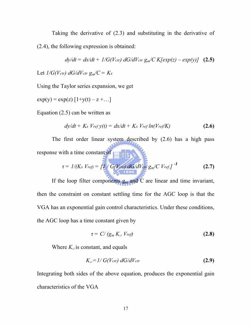
Taking the derivative of (2.3) and substituting in the derivative of
(2.4), the following expression is obtained:
dy/dt = dx/dt + 1/G(Vctr) dG/dVctr gm/C K[exp(z) – exp(y)] (2.5)
Let 1/G(Vctr) dG/dVctr gm/C = Kx
Using the Taylor series expansion, we get
exp(y) = exp(z) [1+y(t) – z +…]
Equation (2.5) can be written as
dy/dt + Kx Vref y(t) = dx/dt + Kx Vref ln(Vref/K) (2.6)
The first order linear system described by (2.6) has a high pass
response with a time constant of
τ = 1/(Kx Vref) = [1 / G(Vctr) dG/dVctr gm/C Vref.] -1 (2.7)
If the loop filter components gm and C are linear and time invariant,
then the constraint on constant settling time for the AGC loop is that the
VGA has an exponential gain control characteristics. Under these conditions,
the AGC loop has a time constant given by
τ = C/ (gm Kx1 Vref) (2.8)
Where Kx1 is constant, and equals
Kx1 =1/ G(Vctr) dG/dVctr (2.9)
Integrating both sides of the above equation, produces the exponential gain
characteristics of the VGA
17

G(Vctr)= Kx2 exp(Kx1 Vctr) (2.10)
Where Kx2 is the constant of integration. Notice that the settling time
is a function of the input variable Vref, indicating the system is
fundamentally nonlinear. By changing Vref, the operating point where the
small signal approximation was made changes, and hence the AGC loop
parameters change.
In our AGC circuit design, we have the following relations and
parameters:
G(Vctr) = 35.2 Vctr – 13.6
G(2V) = 56
Vref = 0.5V
C = 2pF
To have a settling time less than 16µs according to 802.11a standard, then
gm should be larger than 0.4µA/V according to equation (2.7).
2.3 AGC Architecture
Figure 2-4 shows the block diagram of the proposed AGC inside the
target receiver. The AGC circuit is composed of four variable gain
amplifiers, peak detector, loop filter, low pass filter, and dc offset
cancellation circuits. The baseband I and Q signals at the mixers output are
18

amplified by high pass amplifiers. Four stages of VGAs are incorporated
throughout the baseband signal path to provide both high gain and dc offset
cancellation. The gain of the VGAs is controlled by a feedback gain control
signal (Vctr.). The peak detector extracts the signal amplitude. This signal
will pass to the loop filter to be compared with a reference voltage. The loop
filter will then generate a dc-like VGA control signal, Vctr. A sixth order low
pass filter is integrated between the first two and the last two VGAs for
channel selection and to reject any continuous wave or modulated
interferers. The fully differential circuit architecture is employed in the
circuit to ensure that it has better common mode noise rejection.
2-4 Principles of Operation
In this section, the principle and circuit design of the main blocks of
the AGC, namely VGA, peak detector, loop filter, and low pass filter will be
presented.
19

H P F
VGA
1 +
VGA
4
in te g ra to r
L P F
VGA
3
MIXER
OU
TPUT
VGA
2
H P F
VGA
1 +
L P F
VGA
3
in te g ra to r
VGA
4
VGA
2
P e a k d e t .
P e a k d e t
L o o p f ilte r
-I
Q
I O U T
Q O U T
-
V c tr
D iv .
D iv .
+
+
in te g ra to r
in te g ra to r
-
-
V re f
Fig. 2-4 The AGC inside the receiver
2-4-1 Variable gain amplifier including dc offset cancellation circuits
There are several ways to vary the gain of an amplifier. As shown in
Fig. 2.5, the gain of a simple differential amplifier can be controlled by its
bias or loading. By tuning the loading RL1 and RL2, the gain at low
frequencies is varied, but its common mode output voltage is also changed
and affects the bias for the next stage. Alternatively, the gain can be varied
by tuning the bias Ib [15]. However, when the signal is large, the bias should
be set to a smaller value to get a smaller gain, in this case, the dynamic range
of the input devices is also reduced. This is opposite to the requirement of a
20

VGA [16]. In addition, the common-mode output also depends on the gain,
and this technique also entails a lot of power dissipation to obtain gain
variation [17].
Fig. 2.5 Existing gain varying techniques
High input-referred offset voltage is one of the most important
drawbacks of MOS analog circuits when compared to their BJT and
BiCMOS counterparts. Typically the offset voltage can be as high as 20 mV,
which can easily saturate the amplifier output stage when the DC gain is
high enough. This problem is even worse in low-supply applications.
Traditional offset cancellation techniques [18][19] usually utilize sampling
circuit and memory components to sample, store and cancel the offset
voltage. As shown in Fig. 2.6, the offset voltage is sensed and stored in a
capacitor during the calibration period, and feeding it back to signal after the
calibration. The main problem with these methods is that they require a
21
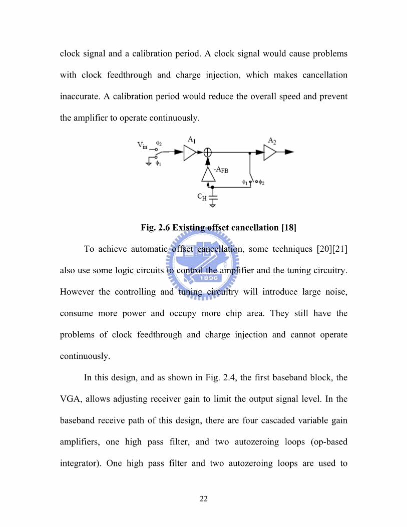
clock signal and a calibration period. A clock signal would cause problems
with clock feedthrough and charge injection, which makes cancellation
inaccurate. A calibration period would reduce the overall speed and prevent
the amplifier to operate continuously.
Fig. 2.6 Existing offset cancellation [18]
To achieve automatic offset cancellation, some techniques [20][21]
also use some logic circuits to control the amplifier and the tuning circuitry.
However the controlling and tuning circuitry will introduce large noise,
consume more power and occupy more chip area. They still have the
problems of clock feedthrough and charge injection and cannot operate
continuously.
In this design, and as shown in Fig. 2.4, the first baseband block, the
VGA, allows adjusting receiver gain to limit the output signal level. In the
baseband receive path of this design, there are four cascaded variable gain
amplifiers, one high pass filter, and two autozeroing loops (op-based
integrator). One high pass filter and two autozeroing loops are used to
22

eliminate the dc offset introduced by VGAs and the previous stages. Two
autozeroing loops and one high pass filter are utilized instead of one
autozeroing loop since the cutoff frequency of the autozeroing loop is
proportional to the gain of the variable gain amplifier. The high pass filter is
placed in the former stage since it has better noise performance than the
autozeroing loop, while autozeroing loops are placed at the latter stages to
reduce the phase introduced by the VGAs.
The proposed AGC is realized with 4 identical VGA cells, as shown
in Fig. 2.4. The gain of each cell can be varied independently from 0 dB to
16 dB by adjusting its own control voltage Vctr.. To achieve a minimum NF,
the gain of the first two stages should be as high as possible [22]. In other
words, when the signal is large, the gain of the third and fourth stages should
be reduced before the gain of first two stages is reduced. However, for large
input signals, the noise requirement of the VGA is actually relaxed.
The schematic of the VGA is shown in Fig. 2-7. In this circuit the
input stage is a degenerated differential pair realized by means of MOS
devices [23], biased in the linear region, shunting fixed value resistors. The
input stage transconductance and therefore the amplifier gain is varied by
varying the MOS resistance via Vctr. To maximize the gain, the resistive load
(R1, and R2) is differential while two PMOS devices (M1 and M2) provide
23

current to the input stage. This configuration requires common mode
feedback (M7, M8, M9, and the current source), but has the advantage of
lower dc voltage drop. The flicker noise of the PMOS current sources has a
negligible impact on the noise figure. To lower out of band blockers, a
differential resistive-capacitive load (C1, C2, R1, and R2) is used to realize
20MHz pole to lower out of band blockers. Moreover, the input devices
(M3, M4) have larger area to reduce the flicker noise. So, this VGA circuit
design meets best the receivers, which require low noise, large gain for a
small input signal and large continuous gain turning range. By turning its
control voltage (Vctr.), its transconductance can be varied and hence its gain.
By varying the Vctr from 0V to 2V, the gain of the VGA sweeps from
minimum to maximum.
Fig. 2-7 The utilized v lifier
V D D
M 2 M 9M 1
V D D
M 3 M 4
M 5M 6
M 7 M 8
V I + V I -
I R E F
V O - V O +
V c t r .
C 1 C 2
V r
R 2 R 1
R 3 R 4
ariable gain amp
24

The variatio e is shown in
Fig.2-8. It is clear that the relation is linear only for small portion of Vctr.
Since
n of the VGA gain with the control voltag
the receive path contains four VGAs, they can be tailored to better
approximate a linear-in-dB characteristic. It can be done using two control
voltages. One (Vctr.) is connected to the first two VGAs and the other one
(0.4Vctr.) to the rest two VGAs. This will make the control curve more linear
and achieve a smaller gain turning sensitivity. In this design, the gain of the
cascaded four VGAs will change from –10dB to 56dB when Vctr changes
from 0V to 2V.
Fig. 2-8 Gain variation of the VGA versus frequency
25

Since s. Each
two stages have an independent gain control. Different gain distributions
give d
1/A2IP
et to maximum gain, the noise figure of the
whol
well. F
. For the sensitivity of -82dBm,
the dynamic range of the wanted signal is -10dBm - (-82dBm) = 72dB.
the AGC consists of a cascade of 4 identical VGA stage
ifferent NF and IIP3 of the whole AGC. Assume A1, A2, A3, A4 are
gain of first, second, third, fourth stage. F1, F2, F3, F4 are noise factors.
AIP31, AIP32, AIP33, AIP34 are input referred interception points. The
noise factor of the whole AGC, F, is then:
F= F1 + (F2-1)/(A21) + F3-1/(A2
1A22) + F4-1/ (A2
1A22A2
3) (2.11)
And the IIP3 of the AGC is:
3 = 1/A2IP31 + A2
1/A2IP32 + A2
1A22/A2
IP33 + A21A2
2A23/A2
IP34 (2.12)
When all stages are s
e AGC is minimized, however the IP3 is degraded to minimum value as
or a large input signal, the total gain of the AGC will be decreased to
a smaller value. Since the signal power is large, the noise contribution from
the AGC is not important any more, the gain of all stages can decrease at the
same time. The IIP3 of the whole amplifier can also be improved when the
gain in the first and second stage decreases.
The variable gain amplifier (VGA) is used to amplify the signal
further and reduce the signal dynamic range
26

Becau
e system (required by 802.11a standard) = 10dB
VGA is also more relaxed because the
by the low pass filter. Because the gain
P3 of the VGA is varying too. Therefore, the
lineari
to monitor the
trength of the signal. The structure of the differential peak detector is shown
l diode can be constructed using the unidirectional
se of gain in previous stages, the NF requirement of the VGA is
relaxed. Assume F>>1,
NFvga≈NFsys + Gainlna + Gainmix + Gainfilter - 3
In this proposed receiver, we have:
NFsys: noise figure of th
Gainlna: gain of the LNA = 19dB
Gainmix: gain of the mixer = 0dB
Gainfilter: gain of the filter = 7dB
= 10 + 19 + 0 + 7 -3 = 33 dB.
The IIP3 requirement of the
interference signals are suppressed
of the VGA is varying, the II
ty of the VGA is defined in output-referred IP3 (OIP3)
2.4-2 Peak detector
In the feedback loop, we should use a peak detector
s
in Fig.2-9. The idea
current mirror [24].
27
VDD
VI+M 9
M 1 M 2
VI -
Ibias
M 3 M 4 M 5 M 6 M 7 M 8
M10 M11 M12
Ibias
c Ie
Ven
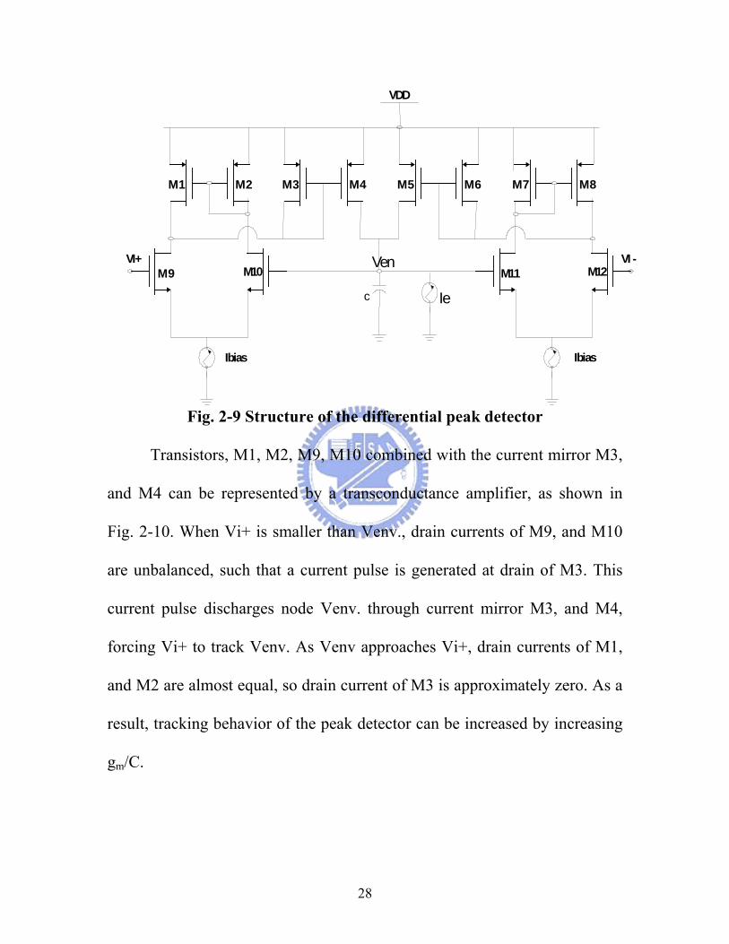
Fig. 2-9 Structure of the differential peak detector
Transistors, M1, M2, M9, M10 combined with the current mirror M3,
and M4 can be represented by a transconductance amplifier, as shown in
Fig. 2-10. W , and M10
are n
hen Vi+ is smaller than Venv., drain currents of M9
u balanced, such that a current pulse is generated at drain of M3. This
current pulse discharges node Venv. through current mirror M3, and M4,
forcing Vi+ to track Venv. As Venv approaches Vi+, drain currents of M1,
and M2 are almost equal, so drain current of M3 is approximately zero. As a
result, tracking behavior of the peak detector can be increased by increasing
gm/C.
28

VDD
c
+
-
Ven.
Vi+gm v
Ie
Fig. 2-10 Equivalent circuit of the peak detector.
2.4.3 Loop f
The gain of the VGA block is c ctr,
by the loop filter. The loop filter is composed of a two
ilter
ontrolled by the control voltage, V
which is generated
inputs transconductance cell (gm-cell), and a loading capacitor, C as shown
in Fig. 2-11. The output of the I and Q peak detectors are summed together
and applied to the input of the loop filter. The sum of these two input signals
will be compared with a reference voltage value, Vref, to generate Vctr.
Table I shows the component values and channel dimensions of the
MOS devices of all the circuits building the AGC.
29

+-
+- C
Vctr
Peak detector
Reference volt.
gm
Fig. 2-11 Structure of the loop filter
Device Value M1, M2 15µm/0.18µm M3,M4 80µm/0.18µm
M5,M6,M9 5µm/0.18µm M7 4µm/0.18µm M8 10µm/0.18µm
C1,C2 1pF R1,R2 2.9K
Variable Gain Amplifier
R3,R4 6.9K M1,M2,M3,M6,M7,M8 10µm/0.18µm
M4,M5 11.5µm/0.18µm M9,M10,M11,M12 15µm/0.18µm
Envelope Detector
C 2pF
Table I Component values and channel dimensions of MOS devices of
the AGC.
30

2.4.4 Low pass filter
The design of full CMOS continuous-time filters can be realized with
MOSFET-C or OTA-C techniques. However to achieve low power supply
voltage and to achieve at the same time low-distortion specifications, the
OTA-C technique is preferred. Even preferred, such filters introduce two
problems. First of all, the OTA is not very linear. Its third-order harmonic
distortion is given by:
HD3= (Vp)2/(32(Vgs-Vt)2) (2.13)
Where Vp is the maximal input amplitude, peak. It follows that a Vgs–Vt of
0.5V gives an HD3 of 0.125% when Vp is 100 mVp.
Another source of nonlinearity in the filter is the presence of junction
capacitors. Its effect depends on how much of the total capacitance is made
out of junction capacitance. It is calculated in [25] that the HD3 is in the
order of –60 dB or 0.1% when half the integrating capacitance consists of
junction capacitance.
The required integrated low pass filter should satisfy the following
technical specifications:
- Simulated LC ladder, resistive terminations
- Passband frequency from zero to 10MHz.
- Passband ripple should be less than 0.5dB.
31

- Stopband frequency should be larger than 20MHz.
- Stopband attenuation larger than 23dB.
With reference to filter tables [26], a third order elliptic filter function
will satisfy the requirements. The transfer function is found to be
H(s)= 0.28163(s2+3.2236)/((s+0.7732)(s2+.4916s +1.1742)) (2.14)
H(s) can be realized as a resistively terminated LC ladder. The circuit with
normalized elements is shown in Fig. 2-12. Leaving the impedance level
open for now but rescaling the components for the required frequency, Wp =
2π(10M) rad/s, results in
Rs = RL =1 C1v = C3v = 1.293/(2π(10M)) µs = 20.58 ns
C2v = 5.89 ns Lv = 13.32 ns
The complete ladder simulation is given in Fig. 2-13.
If we choose gm = 200 µs and for convenience makes 1/gm equals the
normalizing resistor, the required elements become
1/Rs = 1/RL = 200 µs
C1 = C3 = C1v gm = 4.11pF
C2 = C2v gm = 1.18 pF
CL = Lv gm = 2.66 pF
32

Considering that these capacitors are small and that three of them will
further be divided by 2 as shown in Fig. 2-13, we should take into
consideration the effect of the unavoidable parasitic input and output
capacitors of the transconductance elements. From the circuit diagram of
Fig. 2-13, we can see that 2(Ci+Co) appear in parallel with 0.5CL, and
0.5C3, and that 2Ci+3Co shunts 0.5C1. It can be noticed that all parasitic
capacitors can be taken care of by absorption without increasing the degree
of the transfer function. The values of these parasitics depend on the details
of the transconductance design. A suitable differential input-differential
output device is given in [27], where Ci and Co values of 0.42pF and
0.22pF, respectively are claimed. Using these values, the final capacitors for
the design are computed as follows:
0.5C1 = 0.55pF
C2 = 1.18pF
0.5 C3 = 0.78pF 0.5 CL = 0.05pF.
L
C2C3 C1
Rs = 1
RL = 1
Vi Vo C1= 1.29C2=.37C3=1.29L = .837
Fig. 2-12 Required elliptic low pass ladder
33

-
-
-
-
-
Vo+
Vo-
C2
C2
Vi+ Vi--
+ -+
+
-
-+
-+
+
-
+ - +
- + -
+ +
--+
+-
- + .5C
3
.5C
L
.5C
1Fig. 2-13 Third-order Gm-C low pass filter
To increase the stop band attenuation of the needed filter to about
46dB, two third-order Gm-C filters were cascaded.
A full CMOS low-distortion OTA structure, which has inherently
common-mode feedforward (CMFF) is shown in Fig. 2-14
Fig. 2-14 Fully differential OTA with inherent CMF
34

2.5 Simulation Results
The variation of the gain of the four-cascaded VGAs versus the
control voltage is shown in Fig. 2-15. The relation is almost linear. The gain
changes from –10dB to 56dB as the control voltage changes from 0V to 2V.
To reject dc offsets which would result from self-mixing of the mixers
or receiver baseband mismatches, and result in clipping of the subsequent
stages if not properly removed, some form of a high pass filter would have
to be used. In this design, there are four variable gain amplifiers distributed
in the receive path. The poles of these high pass amplifiers cannot be too
low, as they would result in long transient settling during gain changes. On
the other hand, poles cannot be placed too high since this will attenuate the
lowest OFDM subcarriers (located at 312KHz) and thus system performance
through degrading its signal-to-noise ratio. In this design, the poles are
placed at 106KHz. For OFDM modulated signals; which has 52 subcarriers;
the lowest subcarriers are located at ±312KHz, and the highest subcarriers
are at ±8.125MHz, so none of the subcarriers are attenuated by the filter in
the receive chain. The frequency response of the four VGAs that comply
with the above requirements is shown in Fig.2-16. The bandwidth of the
VGA is slightly above 20MHz, to compensate for the parasitic capacitor of
the high pass filter which will in turn decreases the bandwidth.
35

Fig. 2-15 The gain turning curve of the four-cascaded VGAs
Fig. 2-16 Frequency response of the four-cascaded VGAs.
36

Variation of the cascaded four VGAs gain and THD with input power is
shown in Fig. 2-17. The gain reaches the maximum when the input signal is
around –60dBm. If the required THD must be larger than 15dBc, then the
dynamic range of the AGC is 43dB. The main advantage of the utilized
AGC is that it offers continuous control of the received signal rather than
discrete one. The noise figure of the AGC circuit was measured to be
7dB,which means that the increase of the receiver’s noise figure due to AGC
will be acceptable.
Figure. 2-17 Variation of the cascaded VGAs gain and THD with input
power.
37

The waveforms at the outputs of the I, and Q peak detectors are shown
in Fig. 2-18. The Figure shows also the summation of these waveforms that
will be applied to the input of the loop filter.
Figure. 2-18. I and Q peak detector outputs and their summation
38

To measure the stop band loss of the VGA and LPF, two tones were
inserted at the VGA input; one with frequency of 5MHz, and the other with
25 MHz, as shown in Fig.2-19. The 5MHz tone was amplified by 37 dB,
while the 25MHz one was attenuated by 17 dB. So the stop band loss is 54
dB. The frequency response of the elliptic sixth-order low pass filter is
shown in Fig.2-20. Its cutoff frequency is 10MHz.
Table II summarizes the simulation results of the AGC and low pass
filter.
(a)
39

(b)
Figure. 2-19 (a) Amplification of a 5MHz tone. (b) Attenuation of a 25MHz tone.
40

Figure. 2-20 Frequency response of the LPF
Fig. 2.21 shows the gain of the VGA as a function of offset voltage. An
input signal of -60dBm at 5 MHz is applied to the VGA input together with
a DC offset voltage. As the offset voltage varies around the zero, the gain of
the VGA also varies. Without offset cancellation, the gain is very sensitive
to the input offset voltage. Even an offset voltage as small as 0.5 mV at the
input will be amplified by the VGA to more than 0.5 V, and the operation
point of the VGA will be shifted far away from the optimum value, which
results in a significant drop of the gain. However, with offset cancellation,
the offset voltage at input is not amplified and has little effect on the
operation point, and as a result, the gain of the VGA is quite insensitive to
the input offset voltage.
41

Fig. 2.21 VGA gain variation due to offset voltage (a) With offset cancellation
(b) Without offset cancellation
Performance Hspice simulation results
AGC passband range 106KHz~20MHz AGC voltage gain -10~56dB AGC noise figure 7dB AGC dynamic range 60dB LPF cutoff frequency 10MHz LPF power consumption 14mW LPF harmonic distortion 40dB AGC Power consumption 11 m W
Table II Simulated AGC & LPF performance
42

Chapter 3
THE DESIGN OF THE 5GHz DIRECT
CONVERSION RECEIVER
3.1 Receiver Fundamentals
In this section, some fundamental issues concerning direct conversion
receivers front-ends are discussed, e.g. sensitivity, nonlinearity, noise figure,
and phase noise.
Wireless products, e.g. mobile phones, pagers, wireless local-area-
network (LAN) etc., usually consist of several basic blocks including
transceiver front-ends and base-band back-ends. A transceiver front-end is a
combination of a receiver front-end and a transmitter front-end. A receiver
front-end converts a received radio frequency (RF) signal from an antenna
into a baseband signal and a transmitter front-end converts a baseband signal
into an RF signal and sends it to an antenna. In the receiver, the conversion
is done by a few of frequency domain operations including downconversion,
filtering and amplification. The frequency domain operation is realized in
physical building blocks including LNA, mixers, and synthesizer. Those
building blocks are not perfect. Besides the wanted frequency domain
operation, unwanted operations are also performed. Those unwanted
43

operations include adding noise to the signal and distorting the signal.
Therefore the performance of a receiver is limited.
The performance of a receiver is defined as the output signal-to-
unwanted-signal ratio (SUSR). This ratio is taken at its output, before
demodulation and after analog-to-digital (A/D) conversion.
3.1.1 Sensitivity
The sensitivity is a measure of receiver performance. Although the
performance of a wireless communication system is often specified in terms
of the bit error rate (BER), the frame error rate (FER) and the residual bit
error rate (RBER), those specifications are very impractical for the receiver
front-end design. As a receiver front-end can only be evaluated by adding
unwanted signals, such as noise, image signals and intermodulation signals,
to the wanted signal, the performance can therefore be translated into the
specification of signal-to-unwanted-signal ratio (SUSR), which can also be
called as signal-to-noise ratio (SNR), if all unwanted signals are treated as
kinds of noise. An approximate value for this SUSR can be found by means
of BER simulations. For the 802.11a WLAN system, the required SUSR is
10dB. The sensitivity of a receiver is defined as the minimum signal power
at the input of the receiver when a minimum SUSR of 10dB is achieved at
44

the output of the receiver. In the proposed application, a sensitivity of –
82dBm at a data rate of 6Mb/s, and a sensitivity of –65dBm at 54Mb/s is
required.
3.1.2 Linearity
Many RF and analog circuits can be approximated with a linear model
to obtain their response to small signals. Nonlinearity often leads to
interesting and important phenomena. For simplicity, a nonlinear system can
be modeled as follows:
y(t) ≈ α1 x(t) + α2 x2(t) + α3 x3(t) (3.1)
Higher orders are assumed to have much smaller gain and are therefore
ignored.
Nonlinearity of analog circuits will cause problems of harmonics, gain
compression, desensitization, intermodulation, etc. [28]. Intermodulation is
commonly used as a measure of linearity of a circuit. Two-tone test is
usually used to measure the intermodulation of a circuit. As shown in Fig.
3.1, the amplitude of the input signal is swept from small power to large
power. The output signals are measured at both the fundamental frequency,
ω1 or ω2, and the IM3 frequency, 2ω1 - ω2 or 2ω2 - ω1. Two curves can be
plotted in log-scale based on the measured amplitude of both fundamental
45

and IM3 components. There is an intersection point if the two lines are
extrapolated. This point is called third interception point (IP3). Input
referred IP3 (IIP3) is often used to specify the linearity of a system.
Fig. 3.1 Two-tone test of a nonlinear system
In a system with cascading of several stages, the IIP3 of the system,
A2 IP3, can be expressed as:
Where A2 IP3,I is the IIP3 of ith stage and α2
1, β21,... are gain of each stage.
3.1.3 Noise figure
RF circuits always suffer from a noise problem. Noise can be defined
as random interference unrelated to the desired signal. It is a kind of
unwanted signal. But unlike harmonics and intermodulation, it is not a
deterministic signal. For RF circuits built on CMOS technology, there are a
46

few types of noise, e.g. thermal noise, shot noise, flicker noise need to be
considered.
In analog circuit design, signal-to-noise ratio (SNR) and noise figure
(NF) are commonly used to specify the noise performance of a system. SNR
is defined as a ratio of signal power over noise power. NF is defined as a
ratio of SNR at the input of a system over SNR at the output of the system,
i.e. SNR=Psignal/Pnoise, NF=SNRin/SNRout
Assume a system, matched to 50-Ω impedance, has power gain of A2,
and internal input referred noise of Po and it is connected to a source with
source noise of Pn,s. Then the NF is:
NF=SNRin/SNRout
= (Ps,in/Pn,s) / (Ps,out/Pn,out)
=(Ps,in/Pn,s) / [Ps,in* A2/(Pn,s *A2 + Po *A2]
=1 + Po/Pn,s (3.3)
The source noise, Pn,s, is referred to the thermal noise from a 50-
Ω resistor, i.e. V2n,s=4kTRs∆f, where k is Boltzmann’s constant (1.38*10-23
JK-1), T is the temperature in Kelvins, and Rs is the source resistance (50 Ω),
and ∆f is the bandwidth of interest. At room temperature, T=300oK, a 50
Ω resistor has a noise power of:
Pn,s/ ∆f = 10*log10(kT/1mW) = 10*log10(1.38*10-23*300/0.001) = -174dBm/ Hz.
47

Or in a bandwidth of 200kHz,
Pn,s= 10*log10(kT*∆f/1mW) = 10*log10(1.38*10-23*300*200*103/0.001) = -121dBm
In a system with a few stages in cascade, the overall noise figure
equals to:
NF=NF1 + (NF2-1)/A2 1+(NF3-1)/(A2
1A2 2)+(NF4-1)/(A2
1A2 2A2
3) +... (3.4)
Where NFi is the NF of ith stage and A2 i is the gain of ith stage. From Eq.
(3.4), an important observation can be made. NF of the first stage is directly
added to the NF of the whole system. The NF of each of other stages is
scaled down by the total gain of stages in front of it when referred to the
overall NF. Therefore, to achieve a smaller NF of the whole system, NF1
should be as small as possible. At the same time, the gain of this stage, A21,
should be as high as possible so that noise contribution from following
stages can be reduced.
3.1.4 Phase noise of LO signal
In practice, the local oscillator (LO) signal is not a pure sinusoid
signal. It consists of some noise at frequencies close to ωLO. This is called
phase noise. The phase noise (PN) of the LO signal is defined as the ratio
between the noise power in 1-Hz bandwidth at a certain offset, ∆f, and the
carrier power, as shown in Fig. 3.2:
48

Fig. 3.2 Phase noise of LO signal
PN=10log10[(noise power in 1-Hz bandwidth)/(Carrier power)] (3.5)
Because of the phase noise, the interference close to the RF frequency
will generate some noise located in the signal frequency band, as shown in
Fig. 3.3. Assume the signal has a bandwidth of BW and the power is Ps, and
there is an interference at ∆f with a power of Pi. If the conversion gain is
one, after downconversion, the interference has a similar spectrum as LO
signal. The power of the noise that located within the signal bandwidth is:
Pn_dB=Pi_dB + PN + 10log10(BW) (3.6)
And SUSR=Ps_dB - Pn_dB =Ps_dB - Pi_dB - PN - 10log10(BW).
To achieve enough SUSR, the PN of the LO signal should be as large
as possible, and the minimum requirement is:
PN= Ps_dB - Pi_dB -10log10(BW) - SUSR. (3.7)
49

Fig. 3.3 SNR degradation due to phase noise of the LO signal
3.2 Design Consideration and Performance
Requirements for a 5-GHz WLAN Receiver
There are presently three silicon IC technologies suitable for realizing
circuits in the 5GHz frequency range. Silicon, and silicon-germanium
(SiGe), bipolar devices currently provide the highest performance and enjoy
the customary advantage of a high gm/I ratio, in addition to process
refinements specifically intended to enhance analog and RF performance.
These latter improvements often include special resistor and capacitor
operations that posses some combination of tighter tolerance, reduced
parasitics, and higher Q.
A significant less expensive technology that is used here is the
conventional digital CMOS. Although its inferior gm/I ratio makes CMOS
circuit performance more sensitive to wiring parasitics at a given level of
50

power consumption than for bipolar technologies, the superior linearity of
short channel MOS transistors typically confers a somewhat higher dynamic
range per power than that of bipolars, and this quality is often extremely
important for wireless systems. Another noteworthy factor is the large
number of interconnect layers now commonly available in CMOS logic
processes. For RF applications, these additional layers are indispensable for
fabrication inductors and linear capacitors of high quality.
Performance requirements for the RF signal processing blocks are quite
similar for both the HiperLAN2 and 802.11a standards. This commonality
should not be surprising in view of the similar frequency bands, data rates,
and intended deployment scenarios. Consequently, it is possible for a single
receiver design to comply with both sets of specifications.
To determine the precise target values, we first compute the
specifications for both HiperLAN and 802.11a separately, and select the
more stringent of the two in every case. Here we reduce the specification set
to frequency range, noise figure, maximum input signal level (or input-
referred 1-dB compression point), and limits on spurious emissions.
For the frequency range, it is often acceptable to cover only the lower
200MHz band. The upper 100MHz domain is not contiguous with that
allocation, so its coverage would complicate somewhat the design of the
51

voltage controlled oscillator. Furthermore, that upper 100MHz spectrum is
not universally available. Hence the choice here is to span 5.15-5.35GHz.
The worst-case noise figure requirement for HiperLAN is not directly
specified, but may be readily estimated from the fact that a class C receiver
must exhibit a –70dBm sensitivity over a channel bandwidth of 24MHz.
Assuming conservatively that the predetection SNR must exceed 12dB, the
overall receiver noise figure must be better than:
NF= -144 dBm/Hz-12dB- (-174dBm/Hz) = 18dB Where –174dBm/Hz is the available noise power of the source.
Strictly speaking, the required noise figure for HiperLAN2 and
802.11a receivers is a function of data rate. Since it would be cumbersome to
specify individual noise figures for each possible data rate, the specification
for 802.11a instead simply recommends a noise figure of 10dB, with a 5dB
implementation margin, to accommodate the worst-case situation. As this
target is more demanding than that of the HiperLAN2, a 10dB maximum
noise figure is the design goal for the present work.
As stated previously, HiperLAN specifies –25dBm as the maximum
input signal that a receiver must accommodate, whereas 802.11a specifies a
value of –30dBm. Consequently, -25dBm is the target maximum input level.
Converting these specifications into a precise IIP3 target or 1-dB
52

compression requirement is nontrivial. However, as a conservative rule of
thumb, the 1-dB compression point of the receiver should be about 4dBm
above the maximum input signal power level that must be tolerated
successfully. Based on this approximation, we target a worst-case input-
referred 1-dB compression point of –21dBm.
Finally, the spurious emissions generated by the receiver must not
exceed –57dBm for frequencies below 1GHz, and –47dBm for higher
frequencies, in order to comply with FCC regulations.
The choice of the direct conversion architecture results in a host of
challenges that need to be dealt with in the architectural implementation
and/or in the circuit design of the blocks. Such issues include:
• DC offsets which result from self-mixing of the receive mixer as well as dc
offsets which result from baseband block mismatches and the high gain of
the baseband stages will result in clipping of the subsequent stages if not
properly rejected [29].
• Flicker noise on the receive path can impair the SNR of the lowest index
OFDM subcarriers [30]. The effect of flicker noise can be reduced by a
combination of techniques. As the stages following the mixer operate at
relatively low frequencies, they can incorporate very large devices to
minimize the magnitude of the flicker noise. Moreover, periodic offset
53

cancellation also suppresses low-frequency noise components through
correlated sampling.
• The receive baseband path can have potential oscillation problems due to
the fact that most of the receive path gain is implemented at a single
frequency (baseband).
The CMOS RF receiver circuits include low noise amplifier, down
conversion mixers, voltage controlled oscillator, low pass filter, and
automatic gain control circuit. Such circuits will be described in the
following sections.
3.3 Low Noise Amplifier
The first block in most wireless receivers is the low-noise amplifier
(LNA). Since it is the first block, the weak signal from the antenna is applied
to the LNA directly. Therefore, the LNA is required to provide a high gain,
otherwise the noise of subsequent stages, such as the mixer and the low pass
filter, will decrease the SNR at the receiver output. However, if the gain of
the LNA is too high, the linearity requirement of the following stages will be
too high. Because the noise from LNA is added to the weak signal directly
without any reduction of previous gain stage, the noise figure of the LNA
itself must be minimized.
54

So the LNA is responsible for providing signal amplification while not
degrading signal-to-noise ratio, and its figure sets a lower bound on the noise
figure of the whole system. Of primary interest is insight into designing
LNA with low noise figure, good amplification level to the input signal, and
low power dissipation [31].
The schematic of the LNA is shown in Fig. 3-4. It is a differential
common-source amplifier. The gate and source spiral inductors L (9nH) and
Ls (2.3nH) are used with the 2pf capacitor C2 to achieve 50-Ω input
impedance matching. The input transistor M1 is biased at 4 mA to attain an
acceptable level of noise and gain performances. Lower power consumption
could be attained at the expense of higher noise. Cascode transistor M2
enhances the amplifier reverse isolation parameter (S12), and reduces the
LO leakage from the mixer back to the LNA input. The capacitor C at the
output blocks the second-order intermodulation products generated in the
LNA [32]. This capacitor forms with inductor L1 a network that is necessary
for optimal power transfer to the next stages. The common mode rejection
ratio of the LNA is 40 dB.
The input impedance of the LNA must be matched to 50 Ω, so that the
signal from the antenna won’t be reflected and a maximum power transfer
from antenna to LNA can be obtained. There are several topologies, which
55

could be used in the input matching of a LNA [33], 50-Ω resistor matching,
1/gm matching, and inductive degeneration matching. Inductive source
degeneration, as shown in Fig. 3.5, can achieve a better noise figure.
V D D
M 1 M 3
M 2 M 4
L 1 L 1
V I + V I -L L
C
C
L s L s
L B = 2 n H
V O
L B = 2 n H
C 2 C 2
Fig. 3-4 LNA schematic
Fig. 3.5 Inductive degeneration used as input matching
The input impedance looking into the matching network, Zin is:
56

Where Rg and Rl represent the series resistance of the on-chip inductor L and
Ls, C1 is the parallel combination of C2 and Cgs. The resonant frequency is
At resonant frequency, the impedance becomes a pure resistor,
Zin(ωo) = ωT Ls + Rg + R l (3.10)
The input-matching network works like a gain stage with the gain
depending on the value of the capacitor C1. The smaller the capacitor gets,
the larger the voltage Vgs is, and therefore, the larger the gain becomes. To
reduce the noise contribution from the following stages including the input
devices of the LNA, C1 is to be minimized. However, to reduce the C1
(assuming C2 is constant) the input transistors have to be small in size which
results in small gm and in turn degradation in the gain and noise performance
of the whole LNA. In addition, to keep the same resonant frequency, larger
inductors, (L + Ls), have to be used for the small C1, which have larger
resistive loss, lower Q and larger noise contribution. Consequently, careful
57
tradeoffs have to be made between the transistor size and the inductors to
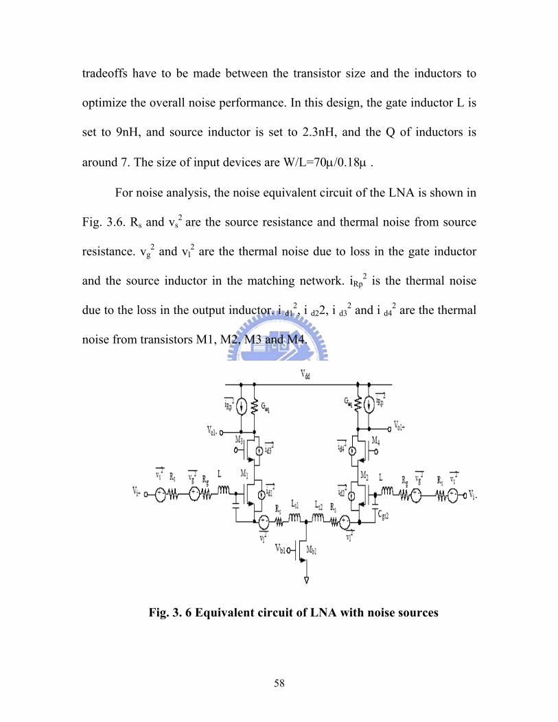
optimize the overall noise performance. In this design, the gate inductor L is
set to 9nH, and source inductor is set to 2.3nH, and the Q of inductors is
around 7. The size of input devices are W/L=70µ/0.18µ .
For noise analysis, the noise equivalent circuit of the LNA is shown in
Fig. 3.6. Rs and vs2 are the source resistance and thermal noise from source
resistance. vg2 and vl
2 are the thermal noise due to loss in the gate inductor
and the source inductor in the matching network. iRp2 is the thermal noise
due to the loss in the output inductor. i d12, i d22, i d3
2 and i d42 are the thermal
noise from transistors M1, M2, M3 and M4.
Fig. 3. 6 Equivalent circuit of LNA with noise sources
58

The transconductance of the input stage of the LNA including the
matching network is:
At the resonant frequency, the imaginary part vanishes and the real
part equals 2Rs.Therefore Eq. (3.11) can be revised as:
The noise factor of the LNA [33] is:
From equation Eq. (3.12), the equivalent Gm of the LNA is
independent from the gm of the input device, as long as the unit gain
frequency, ωT, of the device is fixed. From equation Eq. (3.13), the output
noise due the source noise is also independent from the gm of the input
devices for a fixed unit-gain frequency, ωT. Therefore, the best method to
improve the noise performance of the LNA is to increase the unit-gain
frequency, ωT, of the input devices by increasing the bias current of the input
59

devices or reducing the Cgs of input devices. However, a smaller Cgs needs a
larger L to maintain the same resonant frequency, and a larger L will have
more loss and cause more noise. Therefore, a trade-off must be made
between L and Cgs to optimize the NF of the LNA.
The component values and channel dimensions of the MOS devices of
Fig. 3-4 are summarized in Table III.
Devices Value
M1, M3 70µm / 0.18µm
M2, M4 60/µm / 0.18µm
L, LS, L1 9nH, 2.3nH, 2.3nH respectively
C2 2pF
C 2pF
Table III Component values and dimensions of MOS devices of the
LNA.
3.4 Quadrature Down Conversion Mixer In the RF mixers, the important design parameters are noise figure
(NF), conversion gain (CG), third-order input intercept point (IIP3), and port
60

-to-port isolation. These parameters should be designed to meet the
requirements of various standards for different wireless communication
systems.
In this design, the mixer is intended to be used as the RF
downconversion block in the wireless receiver shown in Fig. 1-1. As seen
from that Figure, the mixer is placed after the low noise amplifier (LNA).
The LNA provides sufficient power gain to mask the noise contribution of
the subsequent stages. Thus the noise figure contributed by the mixer can be
ignored if its value is lower than the total gain of the previous stages.
Since the LNA has provided sufficient gain, the conversion gain of the
mixer should not be high to overdrive the subsequent stages. Higher gain
also implies higher signal swing in the circuit, which could degrade the
linearity and the dynamic range. Nevertheless, very low gain far below 0dB
is also unacceptable because the noise contributed by the stages after the
mixer becomes higher. Thus the value of conversion gain around 0dB is
acceptable.
In the modern wireless systems, the receiver could subject to an
environment with large adjacent channel interfering signals. Due to the
nonlinearity of the receiver, those interfering signals produce co-channel
interference, which degrades the signal-to-noise-ratio of the received signal.
61

Thus IIP3 of the receiver, which indicates the ability of the receiver to reject
the interfering signals becomes a very important feature of the RF receiver.
In most cases, the signal power handled by the RF mixer is higher than those
by the other stages in the receiver. Thus IIP3 of the mixer is a critical
parameter in the receiver design. In order to sustain a high receiver linearity,
IIP3 of the mixer should be as high as possible.
The port to port isolation and LO power are also important issues in
the mixer design. The LO power in the order of a few dBm is often required
by the mixer to obtain high linearity and high dynamic range. Such a high
LO power causes the LO energy leaks through the RF port and radiates from
the antenna if the port isolation of the mixer is not high enough. The design
criteria of the mixer is to keep the LO power as low as possible and
increases the port isolation.
LTI system cannot provide outputs with spectral components not
present at input. So, mixer must be either nonlinear or time varying in order
to provide frequency translation. Mixer performs frequency translation by
multiplying two signals (with their harmonics) in time domain.
Since the MOS transistor is basically a square-law device, then it can
be used to implement second-order transfer functions [34]. In this receiver,
the utilized mixer is a quadrature one, and Fig. 3-7 shows the circuit diagram
62

of the in-phase output of the mixer. In this circuit, type-A combiner consists
of eight transistors (M9~M16), while type-B combiner consists of four
transistors (M17~M20]. The transfer function of the two combiners can be
modeled by the drain current equation of the MOS transistors in the
saturation region. Using the ideal square law current identity of MOS
transistors, the drain current ID can be expressed as
ID = K (VGS – VT) 2 (3.14)
Where K= µs (Cox/2)(W/L) is the transconductance parameter, µs is the
effective surface carrier mobility, Cox is the gate oxide capacitance per unit
area, W/L is the channel width (length) of the MOS device, VGS is the gate-
source voltage, and VT is the threshold voltage.
If the transistors in the type-A combiner are operated in the saturation
region, the output voltage at the their drains terminals can be written as
functions of the input signals LOQ+, LOQ-, RF+, and RF- by using (3.14).
The same thing can be done for the B-type combiner.
The supply voltage of the mixers can be as low as 1.8V, since only
two transistors are cascaded between power supply and ground. By the way,
the down-conversion mixers and VCO share the same current and so the
power consumption will be reduced obviously. In comparison with other
architectures, the current- reused method, as shown in Fig. 3-8, particularly
63

highlights the advantages of the low-power consumption in direct
conversion architectures.
M9 M10 M11 M12 M13 M14 M15 M16
M17 M18 M19 M20
VB VB VB VB
Voi
VDD VDD VDD VDD
+LOI
+RFI
-LOI
-RFI
-LOQ
-RFQ
+LOQ
+RFQ
VDD
R
Fig. 3-7 In phase output of the down conversion mixer
RF-I RF-Q
LO-I LO-Q
GND
VDD
Mixer
VCO
Baseband
3mA
3mA
3mA
Fig. 3-8 The concept of current reuse technique in the receiver
64

3.5 Merged Quadrature Voltage Controlled Oscillator
Fig. 3-9 The conceptual block diagram of the voltage controlled oscillator
To implement the integrated quadrature VCO, a circuit structure based
on the two-stage ring oscillator with LC-tank loads is proposed [35]. As
shown in Fig 3-9 two fully differential narrow-band LC-tuned inverters are
connected to form a two-stage ring oscillator structure for signal oscillation.
The output waveforms at the differential output nodes of one inverter are
90° out of phase from those at the differential output nodes of the other one.
Thus, these two differential output waveforms are synchronized in
65
quadrature phases [35]-[37]. When the delay time of the two fully
differential inverters are kept the same at oscillation, the outputs of these two
fully differential inverters can provide highly accurate quadrature signals. By
incorporating the LC-tank loads into two-stage ring oscillator, the
performance of proposed quadrature VCO is significantly improved with
respect to the following specifications: phase noise, frequency stability, and
supply voltage sensitivities.
In order to efficiently reduce chip area, power dissipation, and
quadrature phase error, the quadrature VCO is cascoded with quadrature
mixer as shown in the block diagram of Fig. 3-8. As may be seen from Fig.
3-8, the cascoded quadrature VCO and quadrature mixer use the same
current I1 (3mA). In this way, the total power dissipation can be optimized.
Furthermore, the signal paths from quadrature VCO to quadrature mixer can
be kept very short and symmetrical to alleviate the influence on the
quadrature phases of VCO output signals by the parasitic components on the
signal paths. Thus the phase error and amplitude mismatch can be
minimized.
66
M6 M5
VC1
MD1MD2
M1
M2
+ LOI -
L1
R
M7M8
VC1
MD4 MD3
M4
M3
- LOQ +
L2
R
Fig. 3-10 Quadrature VCO schematic
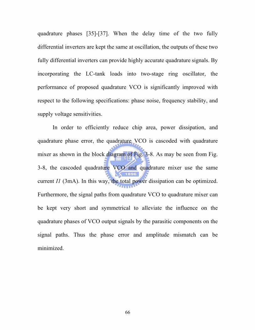
Fig. 3-10 is the circuit diagram to demonstrate the implementation of
quadrature VCO using the two-stage ring oscillator with LC-tank loads. The
MOS transistors M1, M2, M3, and M4 are connected to form a two-stage
ring oscillator to be used as the phase controller. The negative resistor in Fig.
3-10 is realized by two cross-coupled MOS transistors M5 and M6 (M7 and
M8) and connected in parallel with the LC-tank loads to cancel the parasitic
series resistance of spiral inductors and guarantee oscillation.
As shown in Fig. 3-10, the LC-tank loads consists of a spiral inductor
L1 and L2, P+/N-well varactor diodes MD1, MD2, MD3, and MD4, and the
parasitic capacitances of M1, M2, M3, M4, M5, M6, M7 and M8. The two
67

P+/N-well varactor diodes can be tuned simultaneously by the control
voltage VC1 to obtain the desired oscillation frequency expressed as
fosc. = LCπ2/1 Hz.
where L is the inductance of the spiral inductor, and C is the total parallel
equivalent capacitance. The maximum impedance of the LC-tank loads
occurs at the oscillation frequency. At this frequency, the fully differential
inverter achieves the maximum gain and the ring oscillator can maintain the
quadrature oscillation. At other frequencies, the gain of the fully differential
inverters is decreased due to the decrement of the impedance of the LC-tank
loads. Thus the ring oscillator cannot maintain the quadrature oscillation. So
the oscillation frequency is only dependent on L and C of the LC-tank loads.
The component values and channel dimensions of the MOS devices
for the mixer and the VCO are summarized in table V.
Device Value M1~M4 5µm/0.18µm M5~M8 220µm/0.18µm
M9~M16 20µm/0.18µm M17~M20 100µm/0.18µm
R 3K L1,L2 2.3nH
Table V Component values and MOS dimensions of the mixer and the
VCO.
68
3.6 Simulation Results
The receiver’s front-end blocks have been simulated using Hspice
with 0.18µm CMOS technology.
The simulated results of the LNA voltage gain and noise performance with
operating current under 50-Ω system impedance are shown in Fig. 3-11. The
LNA achieves a NF of 2 dB at 5.15 GHz with 4mA current drain from a 2-V
supply. This is the lowest NF reported to date or at least according to my
knowledge for a CMOS LNA operating in the 5 GHz band.
The mixers were also individually characterized and simulated. When
biased with 3mA current and driven by –4dBm LO signal, the mixer has a
conversion gain of 0 dB, and a 7 dB SSB noise figure. Fig. 3-12 shows the
output transient waveforms of the quadrature oscillator. The LO frequency is
5GHz, the phase error is 0.6° and the amplitude error is 2mV.
The quadrature VCO covers a wide operating frequency range, from 5
GHz to 5.5 GHz. The tuning characteristic of the VCO under different
control voltages is shown in Fig. 3-13. The simulated phase noise of the
quadrature VCO is –100dBc/Hz at 500 KHz away from 5.15 GHz center
frequency. The output spectrum of the VCO and the mixer are shown in Fig.
3-14, and Fig. 3-15 respectively. The low power operation of this receiver is
69

enabled by the current reuse technique used among quadrature VCO and
mixer.
Linearity of the front-end of the receiver is evaluated with a two-tone
simulation as shown in Fig.3-16. The input-referred IP3 is –5dBm, with a 1-
dB compression point of –15dBm. This is due to the high linearity of the
short channel MOS- transistors.
The variation of the S11 parameter with frequency for the receiver
front-end is shown in Fig.3-17. It approaches –19 dB at 5.15 GHz
(a)
70

(b)
Fig. 3-11 (a) Simulated LNA voltage gain versus frequency (b) Simulated LNA NF versus frequency.
Fig. 3-12 The output waveform of the quadrature oscillator
71

Fig. 3-13 The tuning characteristics of the VCO.
Fig. 3-14 The VCO output spectrum
72
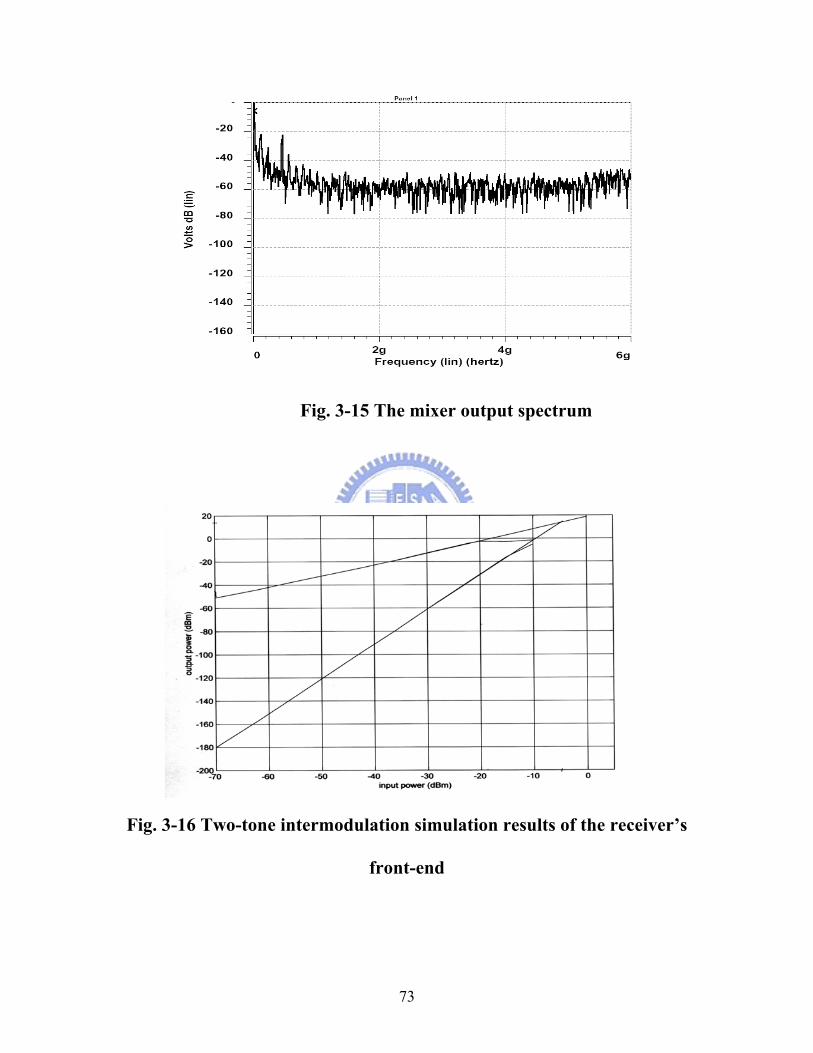
Fig. 3-15 The mixer output spectrum
Fig. 3-16 Two-tone intermodulation simulation results of the receiver’s
front-end
73

Fig. 3-17 Receiver’s front-end S11 parameter versus frequency.
Table IV summarizes the receiver performance.
Performance Hspice
simulation results
IEEE 802.11a Standard. [7]
Noise figure Voltage gain S11 for receiver front-end Input referred IP3 1dB compression point LO leakage to RF Phase noise at 500KHz AGC dynamic range LPF cutoff frequency Power consumption
4dB 80dB -19dB
-7dBm -17dBm -55dBm
-100dBc/Hz 60dB
10MHz 45mW
10 dB - -
-
-26dBm. [7] - - - - -
Table IV Simulated received performance compared to that required by
IEEE 802.11a standard.
74

Chapter 4
POST SIMULATION RESULTS
4.1 Chip Layout Description The layout for one VGA using the CMOS 0.18µm 1P6M technology
is shown in Fig. 4.1.
Fig. 4.1 Layout of one VGA circuit
The overall AGC circuit is shown in Fig. 4.2. The total area is .08mm2
4.2 Simulation Results The post simulation results of the AGC circuit compared to the pre
simulation results are shown in table V. The results are quite close to each
other.
75

Fig. 4.2 Layout of the AGC circuit
Parameter Pre simulation
results
Post simulation
results
Pass band range 106KHz~20MHz 100KHz~20MHz
Voltage gain -10~56dB -10~55dB Dynamic range 60dB 60dB
Power consumption 11mW 10mW
Area _ .08mm2
Table V Comparison between pre and post simulation results for the
AGC circuit
76

Chapter 5
CONCLUSIONS AND FUTURE WORKS
5.1 Conclusions
In this thesis, a 2-V 5-GHz direct conversion receiver has been
designed and simulated using 0.18µm CMOS technology. The receiver
achieves 4dB double sideband noise figure (NF), 90dB voltage gain, -7dBm
input IP3 and dissipating 45mW. The receiver gain is carefully distributed
before and after the mixer to minimize the 1/f noise contribution to the
overall system noise. This receiver achieves the lowest noise figure and
power consumption reported to date for a 5GHz direct conversion receiver.
This receiver complies with the performance requirements of the IEEE
802.11a wireless communications standard for operation at 5GHz.
An automatic gain control (AGC) circuit with high dynamic range is
incorporated inside this receiver. The AGC achieves 7dB noise figure, 66dB
tuning range, and dissipating 11mW. The problem of dc offset appears in
direct conversion receivers due to the imperfect isolation between LO port
and the inputs of the mixer and the LNA is cancelled using ac-coupling
technique including trade-off between degradation of signal-to-noise ratio
due to high cutoff frequency and slower transient related to low cutoff
77

frequency. The large and the continuous gain turning range of the AGC
increases the dynamic range of the receiver. Moreover, as the noise figure of
the AGC circuit is low (7dB), then the increment of the receiver’s overall
noise figure due to the utilization of the AGC is acceptable. Finally, the
obtained results show clearly that CMOS could be used to implement a high-
performance, low power RF circuits in the low-GHz frequency range.
5.2 Future works
In the receiver design, although many simulation results have been
shown to verify the function of the receiver, the hardware implementation is
still needed for further verification. Furthermore, CMOS receiver circuits
operated at lower supply voltages below 2V can be developed to meet the
requirement of the future portable equipment. Moreover, further reduction
in the power consumption, and noise figure of the AGC circuit is still
required. Moreover, a chip for the AGC circuit will be fabricated, and
further measurements on the chip will be carried out.
78

REFERENCES
[1] A. Abidi,” Direct-conversion radio transceivers for digital
communications,” IEEE J. Solid-State Circuits, vol. 30, pp. 1399-1410,
Dec.1995.
[2] B. Razavi,” RF IC design challenges,” in proc. Design Automation Conf.,
San Francisco, CA, 1998, pp. 408-413.
[3] W.A. Serdijin”A Low voltage low power fully integratable automatic
gain control for hearing instruments,” IEEE Journal of Solid-State Circuits,
Vol. 29, No.8, August 1994.
[4] R. Harjani, “A low-power CMOS VGA for 50 Mb/s disk drive read
channel’s,” IEEE Trans. Circuits and Systems-II: Analog and Digital Signal
Processing, Vol. 42, No.6, June 1995.
[5] G.S Sahota, “ High dynamic range variable gain amplifier for CDMA
wireless applications,” ISSCC97, Session 22, February 1997.
[6] Francisco Javier,”a direct conversion receiver using a novel ultra low
power AGC,” ISSCC97, 1997.
[7] IEEE Standard 802.11a-1999: Wireless LAN MAC and PHY
Specification—High Speed Physical Layer in the 5 GHz Band, 2000.
[8] J.F.Wilson et al., “A single-chip VHF and UHF receiver for radio
paging,” IEEE J. Solid-State Circuits, vol. 26, pp. 1944-1950, Dec. 1991.
79

[9] Philips Semiconductors, “Advanced pager receiver, UAA2080T,” in
RF/Wireless Commun. Handbook, 1996.
[10] H.Tsurumi and T. Maeda, “Design study on a direct conversion receiver
front-end for 280 MHz, 900 MHz, and 2.6 GHz band radio communication
systems ,” presented at IEEE Veh.Technol. Conf., St. Louis, MO, 1991,pp.
457-462
[11] J. Wenin, “IC’s for digital cellular communication,” presented at
European Solid-State Circuits Conf., UIM, Germany, 1994, pp. 1-10.
[12] G. Schultes, E. Bonek, A. L. Scholtz, and P. Kreuzgnuber,”Low cost
direct conversion receiver structures for TDMA mobile communications,”
presented at sixth Int. Conf. Mobile Radio and Personal Commun.,
Conventry, UK, 1991, PP. 143-150
[13] A. Batemen and D. M. Haines,” Direct conversion transceiver design
for compact low-cost portable mobile radio terminals,” presented at IEEE
Veh. Technol. Conf., San Francisco, CA, 1989, PP. 57-62
[14] J. Smith, Modern Communication Circuits. New York: McGraw-Hill,
1986, chapter 5.
[15] R. Gomez and A. A. Abidi, “A 50 MHz Variable Gain Amplifier Cell
in 2um CMOS”, Proc. IEEE 1991Custom Integrated Circuits Conf. pp 941-
943, 1991
80
[16] Eric A. M. Klumperink, Carlo T. Klein, etc. “AM Suppression with
Low AM-PM Conversion with the Aid of a Variable-Gain Amplifier”, IEEE
Journal of Solid-State Circuits, Vol. 31, No. 5, May 1996.
[17] C. Srinivasan, K. Radhakrishna Rao, “A 20 MHz CMOS Variable Gain
Amplifier”, Proceedings. Ninth International Conference on VLSI Design,
pp.90-3, 1995.
[18] Ahmad Baghai Dowlatabadi and J.Alvin Connelly, “A New Offset
Cancellation Technique for CMOS Differential Amplifiers”, IEEE
Symposium on Circuits and Systems (Cat. No.95CH35771). IEEE. Part
vol.3, 1995, pp.2229-32 vol.3.
[19] Comino et al. “Offset Correction for a Homodyne Radio”, United States
Patent, No. 5748681.
[20] Chong-Gun Yu, Randall L. Geiger, “An automatic offset Compensation
Scheme with Ping-Pong Control for CMOS Operational Amplifiers”, IEEE
Journal of Solid-State Circuits, Vol. 29, pp 601 - 610, May1994.
[21] James H. Atherton and H. Thomas Simmonds, “An Offset Reduction
Technique for Use with CMOS Integrated Comparators and Amplifiers”,
IEEE Journal of Solid-State Circuits, Vol. 27. No. 8, August 1992.
81

[22] Francesco Piazza, Paolo Orsatti, Qiuting Huang, Hiroyuki Miyakawa,
“A 2mA/3V 71 MHz IF Amplifier in 0.4um CMOS Programmable over
80dB Range”, ISSCC Digest of Technical Papers, pp78-79, Feb., 1997.
[23] Danilo Manstretta, Rinaldo Castello, Francesco Gatta “ A 0.18µm
CMOS Direct-conversion Receiver Front-End for UMTS” IEEE ISSCC
Visuals Supplement, 2002
[24] Sergio A. Sanielevici, Kenneth R.Cioffi “ A 900 MHz Transceiver
Chipset for two way paging applications”, IEEE Journal of solid-state
Circuits. Vol. 33, No. 12, pp. 2160-2168. December, 1998.
[25] J. Silva-Martinez, High performance CMOS continuous-time filters.
Boston, MA: Kluwer, 1992
[26] Rolf Schaumann, M.S. Ghausi “ Design of Analog Filters, Passive,
Active RC, and switched Capacitor”.
[27] Krummenacher, F., and N. Joehl, “ A 4-MHZ CMOS Continuous-Time
Filter with on Chip Automatic Tuning,” IEEE J. Solid-State Circuits, Vol.
SC-23 (June 1988), 750-758.
[28] Jan Crols and Michiel Steyaert, CMOS Wireless Transceiver Design,
Boton: Kluwer Academic Pulishers, p. 109, 1997
[29] Won Namgoong, Tersa H.Meng,” Direct-conversion RF receiver
design,” IEEE transactions on communications, vol. 49.no.3, March 2001.
82
[30] B.Razavi “ Design considerations for direct –conversion receivers”
IEEE transactions on circuits and systems, vol. 44,No. 6, June 1997
[31] Derek K. Shaeffer,”The Design and Implementation of Low Power
CMOS Radio Receivers”, 1999.
[32] Ting-Ping Liu and Eric Westerwick, ‘ 5-GHz CMOS radio transceiver
front-end chipset,”IEEE journal of solid-state circuits, vol. 35, No.12,
December 2000.
[33] Lap Chi LEUNG, A 900-MHz CMOS Bandpass Amplifier for Wireless
Receivers, master thesis, Hong Kong University of Science and Technology,
1999.
[34] S.-Y. Hsiao and C.-Y. Wu,”A parallel structure for CMOS four
quadrant analog multipliers and its application to 2GHz RF downconversion
mixer,” IEEE J. Solid-State Circuits,vol. 33 no. 6, pp. 859-869, June 1998.
[35] C-Y. Wu and H.-S. Kao, “A 1.8GHz CMOS Quadrature Voltage-
Controlled Oscillator (VCO) Using the Constant-Current LC Ring Oscillator
Structure,” in Proc. IEEE International Symp. On Circuits and Systems,
Monterey, California, USA, May 1998, vol. 4, pp. 378-381.
[36] A. Rofougaran, J. Rael, M. Rofougaran, and A. Abidi, “ A 900MHz
CMOS LC-Oscillator with Quadrature Outputs, “in Proc. IEEE ISSCC, PP.
392-393, Feb., 1996.
83

[37] M. Tiebout, “Low-Power Low Phase Noises Differentially Tuned
Quadrature VCO Design in Standard CMOS,”IEEE J. Solid-State Circuits,
vol. 36, pp. 1018-1024, July 2001.
84

PUBLICATION LIST
- CONFERENCE PAPER
[1] Chung-Yu Wu, Ismail Abdel Hafez, “A low-power high dynamic
range AGC for 5GHz direct conversion receivers,” in Proc. Workshop on
Wireless Circuits and Systems (WoWCAS) Conference, Vancover,
Canada, May 21-22, 2004.
85