Embed Size (px)
Citation preview

research papers
242 doi:10.1107/S0021889808042131 J. Appl. Cryst. (2009). 42, 242–252
Journal of
AppliedCrystallography
ISSN 0021-8898
Received 31 July 2008
Accepted 10 December 2008
Odd electron diffraction patterns in siliconnanowires and silicon thin films explained bymicrotwins and nanotwins
Cyril Cayron,a* Martien Den Hertog,b Laurence Latu-Romain,a Celine Mouchet,a
Christopher Secouard,a Jean-Luc Rouviere,b Emmanuelle Rouvierea and Jean-Pierre
Simonatoa
aCEA DRT, LITEN, Minatec, 38054 Grenoble, France, and bCEA, DSM, INAC, Minatec, 38054
Grenoble, France. Correspondence e-mail: [email protected]
Odd electron diffraction patterns (EDPs) have been obtained by transmission
electron microscopy (TEM) on silicon nanowires grown via the vapour–liquid–
solid method and on silicon thin films deposited by electron beam evaporation.
Many explanations have been given in the past, without consensus among the
scientific community: size artifacts, twinning artifacts or, more widely accepted,
the existence of new hexagonal Si phases. In order to resolve this issue, the
microstructures of Si nanowires and Si thin films have been characterized by
TEM, high-resolution transmission electron microscopy (HRTEM) and high-
resolution scanning transmission electron microscopy. Despite the differences in
the geometries and elaboration processes, the EDPs of the materials show great
similarities. The different hypotheses reported in the literature have been
investigated. It was found that the positions of the diffraction spots in the EDPs
could be reproduced by simulating a hexagonal structure with c/a = 12(2/3)1/2,
but the intensities in many EDPs remained unexplained. Finally, it was
established that all the experimental data, i.e. EDPs and HRTEM images, agree
with a classical cubic silicon structure containing two microstructural defects: (i)
overlapping �3 microtwins which induce extra spots by double diffraction, and
(ii) nanotwins which induce extra spots as a result of streaking effects. It is
concluded that there is no hexagonal phase in the Si nanowires and the Si thin
films presented in this work.
1. Introduction
Si nanowires (NWs) are low-dimensional objects with
promising potential in the new, emerging semiconductor
industries. Si NWs could constitute the interconnects and
functional components of the future microelectronic industry
(Cui & Lieber, 2001). They can also be integrated into
photovoltaic solar cells (Tian et al., 2007) or thermoelectric
devices (Hochbaum et al., 2008; Boukai et al., 2008) to enhance
power conversion efficiencies and have a role to play in the
new energy industries. Polycrystalline Si thin films have been
developed for more than 15 years for logic circuit and
videographic applications (Brotherton et al., 1991), and for
first- and second-generation photovoltaic solar cells (Aberle,
2006).
Both Si NWs and Si thin films are developed at CEA–
Grenoble for new energy applications. This study began by a
simple process control of Si NWs by transmission electron
microscopy (TEM). We were unable to index the electron
diffraction patterns (EDPs) of many Si NWs and were
therefore unable to determine their growth directions. We
decided that it was necessary to improve our understanding of
these odd EDPs. There are very few studies in the literature on
odd EDPs in Si NWs; however, peculiar EDPs are often
reported in Si thin films. It was unclear whether the odd EDPs
in Si thin films were the same as those of Si NWs. Odd EDPs
were first reported by Lassen (1934) for face centred cubic
(fcc) metals deposited by vacuum evaporation, but their
origins have not been fully clarified and many hypotheses exist
to explain them. Each is considered in detail below.
1.1. Size effect
The extra spots in the odd EDPs of thin fcc films have been
interpreted by Cherns (1974) as an effect of the finite
sequence of the ABC layers of the (111) planes. In very thin
objects, the sequence is incomplete, i.e. is not a multiple of
three (111) planes, and some hexagonal compact packings
(hcp) remain at the surfaces of the object. They correspond to
a 2H structure and explain the anomalous spots in the EDPs.
Cherns’ interpretation was used to explain odd diffraction in
silicon thin films (Gibson et al., 1989) and in silicon NWs (Bell

et al., 2004) (Si can be considered as the sum of two translated
fcc structures). Based on the same idea, Korgel et al. (2006)
simulated odd EDPs in Si NWs of diameters less than 10 nm.
However, Cherns’ interpretation cannot explain the anom-
alous spots observed in the EDPs of silicon films or nanowires
of thickness or diameter greater than 100 nm.
1.2. Twinning effect
Odd EDPs in gold thin films were explained by Dickson &
Pashley (1962) and by Pashley & Stowell (1963) as double
diffraction between superposed twinned crystals. Such super-
position, called ‘double positioning’, was observed by dark-
field imaging and found to occur at the grain boundaries of the
film. A schematic representation is given in Fig. 1(a).
However, some anomalous spots, such as the extra spots
situated at 1/3{422}, could be explained only by introducing an
unusual notion of double diffraction between non-excited
spots. Buffat et al. (1991) reported odd power spectra of
HRTEM (high-resolution transmission electron microscopy)
images of gold nanoparticles, and these authors could prove,
by convincing image simulations, that the anomalous spots
were due to a superposition of twins and did not result from an
hcp phase. Carim et al. (2001) found one odd power spectrum
in an Si NW oriented in the [111] direction, and they inter-
preted it as the consequence of a twin lying along the growth
direction of the nanowires. Kohno et al. (2003) established, by
convincing simulations, that some extra spots in silicon
nanoparticles are due to the diffraction of microtwins, and that
others, such as the 1/3{422} extra spots, are induced by
streaking effects probably produced by stacking faults (and
not by complex double diffraction as previously imagined by
Pashley & Stowell, 1963).
Pashley & Stowell (1963), Buffat et al. (1991) and, more
recently, Kohno et al. (2003) warned the scientific community
not to interpret the odd EDPs by assuming the existence of
hexagonal silicon phases. However, despite their warning, as
will be seen in the next section, a very high number of papers
still mention new phases in Si NWs and Si thin films.
1.3. Hexagonal silicon structures
More than 12 forms, including the wurtzite 2H structure,
have been reported since 1963 for silicon under high pressure
(Wentorf & Kasper, 1963; Besson et al., 1987). These studies
led researchers to think that such phases could also exist in
metastable silicon elaborated by physical or chemical vapour
deposition processes.
In silicon thin films, the presence of hexagonal phases has
been widely accepted and reported for more than 20 years.
Hendriks et al. (1984) studied by X-ray analysis Si thin films
elaborated by low-pressure chemical vapour deposition
(LPCVD). From new peaks in the angular profiles close to the
classical d(111), these authors proposed the existence of Si
polytypes resulting from a high density of stacking faults or
microtwins. Dahmen et al. (1989) observed by TEM the exis-
tence of 2H silicon at the intersection of two deformation
microtwins in a silicon matrix. A disclination model was later
proposed by Muller & Pirouz (1997) to explain the formation
of this 2H structure. Cerva (1991) confirmed by HRTEM
observations the existence of the 2H Si structure in LPCVD Si
thin films and also observed other 4H and 9R polytypes. The
presence of these polytypes was explained by a stress-induced
martensitic transition at an intersection of crossing twins,
according to the model proposed by Dahmen et al. (1989).
Since then, other studies have reported the existence of the 2H
structure in LPCVD Si thin films by TEM observations
(Nakhodkin et al., 2000) or by Raman experiments (Bandet et
al., 2000).
In these studies, the 2H polytype appears as a sequence of
stacking faults locally ordered on a scale of a few nanometres.
Higher ordering distances can be obtained by artificially
controlling the stacking fault sequence by using multi-step
molecular epitaxy on Si(111) surfaces and boron as surfactant
twinning inducer (Fissel et al., 2006). Many studies also report
the existence of hexagonal forms of silicon in CVD (chemical
vapour deposition) thin films recrystallized by laser excitation.
research papers
J. Appl. Cryst. (2009). 42, 242–252 Cyril Cayron et al. � Odd electron diffraction patterns in silicon nanowires 243
Figure 1Double positioning grain boundary in fcc thin film: overlapping of the twotwinned crystals along the electron direction h111i. (a) Schematicrepresentation (from Dickson & Pashley, 1962). Pashley & Stowell(1963) used this representation and other arguments based on complexdouble diffraction between non-excited spots to explain the extra spots at1/3{422} in the h111i EDPs. (b) We propose another schematicrepresentation of the double positioning grain boundary. Nano-interpenetrating steps at the interface act as planar defects on the {111}planes and induce streaks along the reciprocal vector g(111). The streaksintersect the Ewald sphere and create the extra spots at 1/3{422} (detailsin xx3.1 and 5.2).

Marfaing & Marine (1989) indexed four EDPs and proposed a
hexagonal structure with a = 0.39 and c = 0.94 nm. These
authors did not notice that the c/a ratio of 2.43 is very close to
3ð2=3Þ1=2. This result is strange because the sequence length
usually corresponds to the cubic diamond 3C phase. Another
hexagonal structure with a c/a ratio close to 2.68 was obtained
later by Kim & Lee (1996). More recently, Zhang et al. (1999)
observed odd EDPs in Si thin films deposited by laser ablation
and proposed a simple 2H structure with, however, a large
discrepancy between the experimental and calculated
diffraction spot positions (> 5%). Very similar odd EDPs were
also observed in germanium thin films deposited by CVD and
recrystallized by electron beam (Parsons & Hoelke, 1984) or
by laser excitation (Cesari et al., 1985) techniques, or depos-
ited by laser ablation (Zhang et al., 2000). In Si NWs, some
papers also assume the existence of hexagonal phases to
explain the odd EDPs. Fontcuberta i Morral et al. (2007)
indexed two unusual HRTEM images in Si NWs with a 2H Si
structure (with an error close to 5%). A deeper TEM study
had already been performed on Si whiskers by Miyamoto &
Hirata (1978) – at that time, nanowires were called ‘whiskers’
– and these authors indexed four EDPs with an error far lower
than 5% with a 6H Si structure; they also reported other
hexagonal and rhombohedral polytypes of Si (27R, 51R and
141R).
What is striking in this short review is that all the odd EDPs
reported in the literature seem to be very similar, whatever the
nature of the silicon and the elaboration process. For example,
the power spectrum Fig. 2f given by Fontcuberta i Morral et al.
(2007) in Si NWs looks the same as the EDP of (i) Fig. 2 of
Dickson & Pashley (1962) in a gold thin film, (ii) Fig. 4b of
Buffat et al. (1991) in a gold nanoparticle, (iii) Fig. 4b of Kohno
et al. (2003) in an Si nanoparticle, (iv) Fig. 3b of Miyamoto &
Hirata (1978) in an Si whisker, (v) Fig. 1b of Marfaing &
Marine (1989) in an LPCVD Si thin film, and (vi) Fig. 1c of
Zhang et al. (2000) in laser ablation Si thin film. This pattern
was explained by the presence of hexagonal phases by
Marfaing & Marine (1989), Zhang et al. (2000) and Fontcu-
berta i Morral et al. (2007), and by a superposition of two
diffraction patterns produced by two twinned 3C crystals in
[123]crystal 1 = [321]crystal 2 zone axes by Dickson & Pashley
(1962), Buffat et al. (1991) and Kohno et al. (2003). Another
example is the [111]3C zone axis EDP with 1/3{422} extra spots
given in Fig. 1i of Kohno et al. (2003), Fig. 10 of Pashley &
Stowell (1963), Fig. 3b of Carim et al. (2001) and Fig. 1d of
Zhang et al. (1999). This pattern was explained by hexagonal
phases by Zhang et al. (1999), complex double diffraction by
Pashley & Stowell (1963), and a streaking effect by Kohno et
al. (2003).
In order to provide a good explanation for the odd EDPs in
Si NWs and Si thin films, we have fully characterized these
materials by TEM and HRTEM and simulated as far as
possible the different solutions proposed in the literature. We
will show that the odd EDPs result from both microtwinning
and nanotwinning. This study will therefore confirm and also
complete and correct some details of the Pashley & Stowell
(1963) and Kohno et al. (2003) studies.
2. Experiments
The Si NWs of this study were elaborated by CVD using the
vapour–liquid–solid (VLS) method (Wagner & Ellis, 1964)
with gold as catalyst and SiH4 or SiH2Cl2 diluted in H2 as
gaseous precursors at temperatures between 773 and 1023 K
under a pressure of 10 Torr (1 Torr = 133.322 Pa). Details of
the process are given elsewhere (Latu-Romain et al., 2008).
The Si thin films (2 mm thick) were deposited by electron
beam evaporation onto silicon nitride coated glass substrates.
They were recrystallized in a tubular quartz furnace under an
argon atmosphere at 873 K.
For the preparation of the TEM specimen, the Si NWs were
dispersed in ethanol with ultrasonic apparatus and deposited
onto a Cu grid covered by a thin amorphous carbon layer. A
cross section of one Si NW was also prepared by focus ion
beam (FIB) milling using FEI Strata400 equipment. The Si
thin films were prepared by classical cross section, i.e.
mechanical polishing and ion milling. The microstructural
observations were performed by conventional TEM with a
JEOL 2000FX (200 kV), by HRTEM with a JEOL 4000EX
(400 kV) and by high-resolution scanning transmission elec-
tron microscopy (HRSTEM) with an FEI Titan (300 kV)
equipped with a condenser Cs corrector and a high-angle
annular dark-field (HAADF) detector. The EDPs were
obtained on the 2000FX TEM by using double-tilt and rota-
tion–tilt sample holders. The power spectra (i.e. the square of
the fast Fourier transform magnitude of HRTEM images)
were calculated using a digital micrograph.
3. Simulations of the diffraction patterns
A simple computer program has been written to simulate the
EDPs for any crystallographic structure. There are many other
and more powerful computer programs, such as JEMS
(Stadelmann, 1987), but our program has the advantage of
being integrated in a larger piece of software, called GenOVa
(Cayron, 2007b), dedicated to the calculation of variants. The
simulations are purely kinematical. The dynamical effects are
not taken into consideration; however, optionally, the extra
spots that could come from a double diffraction can be
calculated by linear combinations. Other specific points are
detailed in the following sections.
3.1. Hexagonal silicon polytypes and their relationship withthe cubic phase
GenOVa calculates the diffraction patterns of crystals
linked by an orientation relationship (OR), and it superposes
these diffraction patterns. The OR between an ideal polytype
of type nH (for n even) or nR (for n odd) and the usual cubic
phase 3C is anH ¼ 1=2½1 1 0�3C and cnH ¼ n=3½1 1 1�3C. The
ideal polytype nH (or nR) has lattice parameters
anH ¼ ð1=2Þ1=2a3C and cnH ¼ n�anH, where � ¼ ð2=3Þ1=2. For
example, c2H/a2H = 2� in the wurtzite structure. In the
following, the direct basis of the cubic crystal, denoted DIR3C,
is normalized. The transformation matrix from DIR3C to the
direct basis DIRnH of the nH polytype crystal is given by
research papers
244 Cyril Cayron et al. � Odd electron diffraction patterns in silicon nanowires J. Appl. Cryst. (2009). 42, 242–252

½DIR3C ! DIRnH� ¼1
2
�1 0 2n=3
1 �1 2n=3
0 1 2n=3
24
35: ð1Þ
The metric tensor of the polytype nH, i.e. the transformation
matrix from the reciprocal basis to the direct basis of the
polytype, is expressed by the matrix
½RECnH ! DIRnH� ¼1
4
2 �1 0
�1 2 0
0 0 4n2=3
24
35: ð2Þ
Since [REC3C ! DIR3C] is the identity matrix (because the
reference frame DIR3C is normalized), the transformation
matrix from the reciprocal basis REC3C of the cubic crystal to
the reciprocal basis RECnH of the nH polytype crystal is
[REC3C!RECnH] = [REC3C!DIR3C][DIR3C!DIRnH]�
[DIRnH!RECnH] = [DIR3C!DIRnH][RECnH!DIRnH]�1
and, consequently,
½REC3C ! RECnH� ¼2
3
�2 �1 3=2n
1 �1 3=2n
1 2 3=2n
24
35: ð3Þ
The matrices presented in this section are automatically
calculated by GenOVa. They are used in the simulations of the
EDPs of the polytypes.
3.2. Streaking effects
The computer program also calculates the extra spots
created by diffraction relaxation effects. Indeed, stacking
faults or other planar defects in a crystal degenerate the nodes
of the reciprocal lattice along a vector s normal to the defect
plane. If the defect is thin, the streaks are elongated and can
intersect the Ewald sphere to produce ‘extra’ diffraction spots
as shown in Fig. 2. The algorithm used to calculate the posi-
tions of these extra spots is now detailed. The electron beam is
parallel (no convergence), and the Ewald sphere is reduced to
a plane owing to the small wavelength of electrons in
comparison with the interplanar distances. Consequently, only
diffraction in the zero-order Laue zone is considered in the
simulations. A (111) platelet defect of thickness nd(111) induces
a degeneracy vector s ¼ ð1=nÞgð111Þ. For a given zone axis u,
the number N of Laue zones that intersect the Ewald sphere as
a result of the streaking effect is given by the product of the
norms N ¼ jsj � juj. The vectors g that belong to these high-
order Laue zones (HOLZs) are given by vectors with integer
coordinates in accordance with the equation jg � uj � N. Any
vector g of this list is degenerated and forms a segment given
by g � ks where k 2 [0, 1]. The segment intersects the Ewald
sphere for a real number k 2 [0, 1] such that u � (g � ks) = 0.
The numbers k are easily calculated and the vectors g � ks
constitute the extra spots produced by the streaking effect.
3.3. Twins in a cubic silicon matrix
In this study, we were also particularly interested in twins.
Twins in fcc and diamond structures are (111) mirror
symmetries. The orientation relationship between twinned
crystals is often denoted �3 because the two lattices have one-
third of their nodes in common (Bollman, 1970, 1982). Twins
are frequently observed in low stacking fault energy materials
such as Cu (20–50 mJ m�2), but they are also frequent in
silicon despite its higher stacking fault energy (50–
100 mJ m�2). Twinning mechanisms in silicon are different
from those of copper. In copper, twins are formed during
annealing and recrystallization treatments, whereas in silicon
thin films, twins are probably generated by the shear stresses
induced by the amorphous–crystalline transformation. In Si
NWs, twins are not yet clearly understood, but could result
from the stresses induced by the fast liquid–solid transfor-
mation at the droplet/nanowire interface, or from the possible
presence of impurities in the liquid that modify the stacking
fault energy of silicon and segregate at the twin boundaries,
such as gold atoms (Allen et al., 2008). The boundary between
two twinned crystals is not always the (111) mirror plane. If
necessary, one must specify the interfacial plane in the nota-
tion; for example, a �3{112} is a �3 twin with an interface
plane of type {112} [such interfaces have been observed, for
example, in cast silicon by Kuchiwaki et al. (2005)]. A silicon
crystal has four twinned variants as a result of its four {111}
equivalent planes that act as mirror symmetries. Algebraically,
the orientations of the four variants are given by sets of
equivalent matrices giT with i 2 {0, 1, . . . , 3}, where T is the
matrix representing the (111) mirror symmetry and gi are
symmetry matrices arbitrarily chosen in the four cosets of the
quotient set G/H, where G is the point group of silicon (m3m)
and H is the intersection group. In general, the identity matrix
is chosen for g0. Theoretical details are given elsewhere
(Cayron, 2007a). The four matrices chosen in this study are
T ¼1
3
1 �2 �2
�2 1 �2
�2 �2 1
264
375; g1T ¼
1
3
1 �2 �2
2 �1 2
2 2 �1
264
375;
g2T ¼1
3
�1 2 2
�2 1 �2
2 2 �1
264
375; g3T ¼
1
3
�1 2 2
2 �1 2
�2 �2 1
264
375:
ð4Þ
They are transformation matrices from a basis of a reference
crystal to the bases of its four twinned variants. We use their
inverses to calculate the direction of the electron beam in the
bases of the twinned crystals. For example, the [011] zone axis
in a silicon crystal becomes [411], [411], [011] and [011] zone
axes for the four twins. Since, in this study, we consider that
twinning only occurs in the diamond Si phase (cubic), the
metric tensor is reduced to the identity matrix and the four
matrices [equation (4)] can also be used to calculate the
positions of the diffraction spots of the twin variants in the
reference frame of their parent crystal (this parent crystal is
also, in general, the matrix in which the twin variants are
embedded).
In the following, we will use the term ‘microtwin’ to refer to
a twin inside a parent matrix with size ranging from 30 nm to
micrometres. The microtwins are large enough to diffract as
normal independent crystals but can also produce extra spots
research papers
J. Appl. Cryst. (2009). 42, 242–252 Cyril Cayron et al. � Odd electron diffraction patterns in silicon nanowires 245
by double diffraction with their parent crystal (x3.3). We will
use the term ‘nanotwins’ to refer to very thin twins lying on the
{111} planes, with thickness ranging from one to ten times
d(111). Such nanotwins are nearly two-dimensional objects that
generate the diffraction spots of the parent crystal by a
streaking effect (x3.2). The term ‘nanotwins’ includes the
stacking faults on the {111} planes. All the simulations of the
EDPs (hexagonal phases, micro- and nanotwins) were
performed with our software GenOVa (Cayron, 2007b).
4. Experimental results
4.1. Silicon nanowires
Most of the Si NWs are straight single crystals with
diameters that vary from 20 to 500 nm. From the EDPs
acquired on untilted nanowires and easily indexed by the
diamond structure, we could establish that the growth direc-
tion is generally h111i, quite often h112i and occasionally
h110i. We could not observe any relationship between the
growth directions and the diameters of the nanowires. The
external surfaces of the Si NWs are constituted of {111} and
{311} facets (Fig. 3), which correspond to the planes of lowest
energy for the diamond Si structure. More than 40% of the
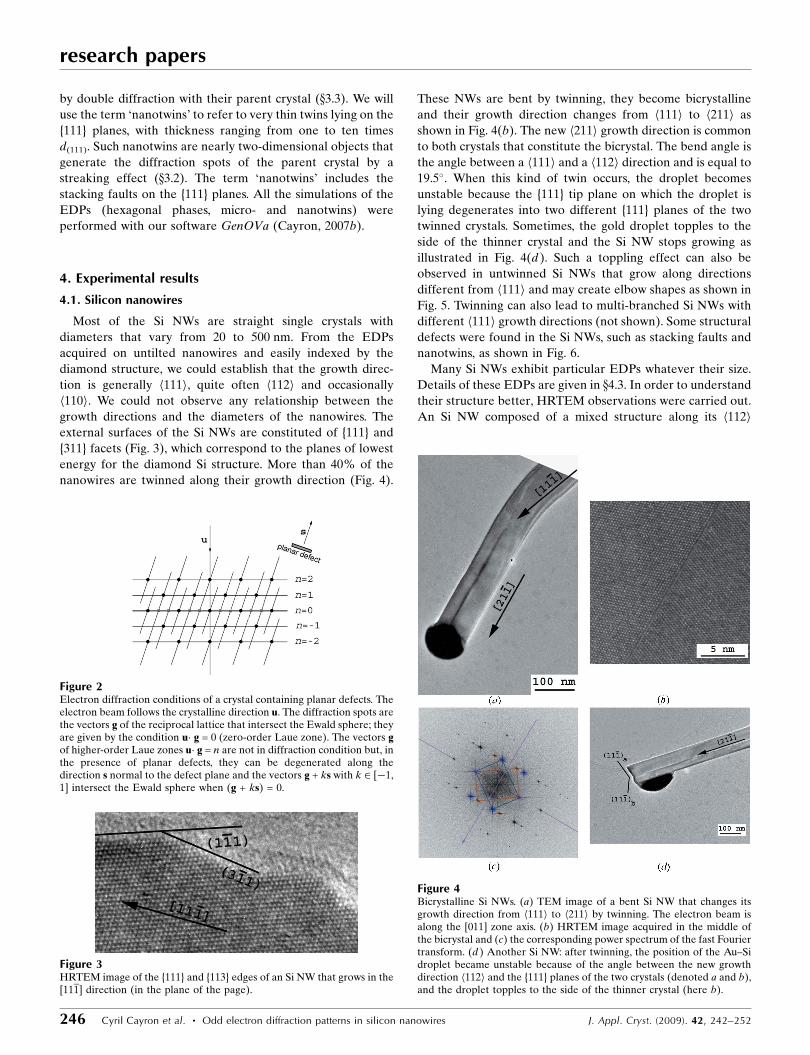
nanowires are twinned along their growth direction (Fig. 4).
These NWs are bent by twinning, they become bicrystalline
and their growth direction changes from h111i to h211i as
shown in Fig. 4(b). The new h211i growth direction is common
to both crystals that constitute the bicrystal. The bend angle is
the angle between a h111i and a h112i direction and is equal to
19.5�. When this kind of twin occurs, the droplet becomes
unstable because the {111} tip plane on which the droplet is
lying degenerates into two different {111} planes of the two
twinned crystals. Sometimes, the gold droplet topples to the
side of the thinner crystal and the Si NW stops growing as
illustrated in Fig. 4(d). Such a toppling effect can also be
observed in untwinned Si NWs that grow along directions
different from h111i and may create elbow shapes as shown in
Fig. 5. Twinning can also lead to multi-branched Si NWs with
different h111i growth directions (not shown). Some structural
defects were found in the Si NWs, such as stacking faults and
nanotwins, as shown in Fig. 6.
Many Si NWs exhibit particular EDPs whatever their size.
Details of these EDPs are given in x4.3. In order to understand
their structure better, HRTEM observations were carried out.
An Si NW composed of a mixed structure along its h112i
research papers
246 Cyril Cayron et al. � Odd electron diffraction patterns in silicon nanowires J. Appl. Cryst. (2009). 42, 242–252
Figure 3HRTEM image of the {111} and {113} edges of an Si NW that grows in the[111] direction (in the plane of the page).
Figure 4Bicrystalline Si NWs. (a) TEM image of a bent Si NW that changes itsgrowth direction from h111i to h211i by twinning. The electron beam isalong the [011] zone axis. (b) HRTEM image acquired in the middle ofthe bicrystal and (c) the corresponding power spectrum of the fast Fouriertransform. (d ) Another Si NW: after twinning, the position of the Au–Sidroplet became unstable because of the angle between the new growthdirection h112i and the {111} planes of the two crystals (denoted a and b),and the droplet topples to the side of the thinner crystal (here b).
Figure 2Electron diffraction conditions of a crystal containing planar defects. Theelectron beam follows the crystalline direction u. The diffraction spots arethe vectors g of the reciprocal lattice that intersect the Ewald sphere; theyare given by the condition u� g = 0 (zero-order Laue zone). The vectors gof higher-order Laue zones u� g = n are not in diffraction condition but, inthe presence of planar defects, they can be degenerated along thedirection s normal to the defect plane and the vectors g + ks with k 2 [�1,1] intersect the Ewald sphere when (g + ks) = 0.

growth direction is presented in Fig. 7; the two sides have a
normal Si structure, but the centre looks like a superstructure
with a periodicity of 3d(111). Similar periodic patterns with
clear atomic resolution were also obtained by HRSTEM
(Fig. 8). Such images could lead us to believe that a silicon
superstructure exists in the Si NWs, but we will see in the
following sections that this is not the case.
4.2. Silicon thin films
The Si thin films deposited onto a glass substrate covered by
an SiN layer are polycrystalline and contain many planar
defects. All the grains also exhibit odd EDPs. Details are given
in x4.3. HRTEM images, such as the one presented in Fig. 9,
are very informative on the nature of the defects. In the very
thin parts of the sample, alternating twins on the {111} planes
are clearly visible, but in the thicker parts the twins cannot be
observed anymore and are replaced by patterns that look like
the superstructure with the periodicity of 3d(111) already
observed in the Si NW. However, the ‘superstructure-like’
patterns in the Si thin films (Fig. 9) are not as clear and
research papers
J. Appl. Cryst. (2009). 42, 242–252 Cyril Cayron et al. � Odd electron diffraction patterns in silicon nanowires 247
Figure 5Formation of a 90� elbow in an Si NW. Such a shape can be explained by atoppling effect. First, the nanowire grows in the h110i direction, but,because of the angle between the {111} tip surface and the growthdirection, the droplet topples at the edge of the nanowire. The nanowirecontinues to grow in epitaxy with the h110i nanowire but in a h111idirection.
Figure 6Nanotwin in an Si NW in the [011] zone axis. (a) HRTEM image and (b)power spectrum of the image. The growth direction is [111] and the twinmirror plane is (111). The nanotwin has a thickness of nine (111) planes,which produces streaks in the power spectrum; one is marked by anarrow.
Figure 7Odd feature in an Si NW in the [011] zone axis. (a) HRTEM and (b)power spectrum. The superstructure-like pattern follows the [211] growthdirection of the NW. A periodicity of 3d(111) is clearly visible in both theimage and the power spectrum. It is shown in x5.2 that such a pattern is, infact, a Moire effect produced by overlapping twins.
Figure 8HRSTEM image of a superstructure-like pattern in an Si NW growingalong the [211] direction. The superlattice seems to have a periodicity of3d(111), and atomic columns inside the lattice are clearly resolved. In thetop right corner is a ‘simulation’ of this superstructure-like pattern thatconsists of a superposition of the twinned parts of Fig. 4(b), as explainedin x5.2.
Figure 9Cross section of an Si thin film in the [011] zone axis. (a) HRTEM imageand (b) power spectrum. The odd feature with a periodicity of 3d(111)
similar to Fig. 7 is visible in the thicker part of the sample (centre of theimage). Its left side, marked by the two inclined arrows, corresponds to avertical (131) plane. The atomic columns cannot be clearly distinguished.The feature is actually a Moire effect produced by the superposition oftwinned crystals. In the thinner parts of the sample, alternating (but notsuperposing) twins are indicated by the horizontal arrows.

periodic as those obtained in the Si NWs (Fig. 7) and, actually,
they look more like Moire patterns than real superstructure.
The interpretation is in x5. Other planar defects on the {113}
planes could also be identified by HRTEM in the thick parts of
the sample (Fig. 10). Such defects have already been identified
and studied by Parisini & Bourret (1993).
4.3. Odd EDPs in Si NWs and Si thin films
The odd experimental EDPs are presented in Figs. 11 and
12, in the first column for the Si NWs and in the second column
for the Si thin films. It is possible to see the great similarities
between the odd EDPs in these two materials. Some of these
patterns clearly correspond to the normal cubic Si structure,
but with additional spots (Fig. 11, column 1 or 2). Other EDPs
cannot be easily indexed with the diamond Si structure
(Fig. 12, column 1 or 2) because some
interplanar distances (such as 0.33 nm)
and angles (such as 61�) do not match
those of Si. The extra spots at 1/3{224}
that have been reported by other
authors (see end of x1) are visible in
Fig. 11, last line. As discussed in x1,
different explanations are possible. The
fact that the odd EDPs are observed
even for NWs larger than 100 nm and
the similarities between those obtained
on the Si NWs and on the Si thin films
allow us to conclude that these EDPs
are not due to size effects as suggested
by some authors (x1.1). This leaves the
possibilities that they are due to
diffraction artifacts produced by twins
(see x1.2) or to the existence of a new
structure of silicon (x1.3).
5. Simulations and discussion
5.1. Odd EDPs are not due to a siliconsuperstructure
At the start of this study, we believed
a hexagonal superstructure existed in
the Si NWs and we tried to determine it
according to the EDPs of Figs. 11 and 12
(first column). We quickly realized that
the wurtzite structure (2H) proposed by
some authors (Zhang et al., 1999; Font-
cuberta i Morral et al., 2007) was not
appropriate because of the very large
discrepancy in the positions of the
diffraction spots between the experi-
mental and theoretical patterns (> 5%)
and the impossibility of reproducing the
intensities in these patterns. The EDP
and the power spectrum obtained along
the h110i zone axis (Fig. 12, first column,
first line, and Fig. 7b) led us to attempt
research papers
248 Cyril Cayron et al. � Odd electron diffraction patterns in silicon nanowires J. Appl. Cryst. (2009). 42, 242–252
Figure 10{113} defects in an Si thin film. (a) HRTEM image in cross section in the[011] zone axis and (b) power spectrum. The defects are situated in the(311) plane as shown by the streaks in the power spectrum.
Figure 11Odd EDPs acquired on Si NWs (first column) and on Si thin films (second column), and theirsimulations with a hypothetical 12H* superstructure (third column) and with a normal cubic Sistructure with diffraction effects produced by microtwins and nanotwins (fourth column). In thesesimulations, we have considered that the four microtwin variants diffract (blue discs). The extraspots due to the streaking effects produced by the nanotwins have been calculated with a uniquedegeneracy vector s = 3g(111) (black dots). The four simulated zone axes are [211], [233], [411] and[111] (in the 3C cubic basis). The zone axes presented in this figure do not allow unambiguousdiscrimination between the two hypotheses (hexagonal superstructure or twin diffraction artifacts).

hexagonal structures with a ratio c/a = 3�, i.e. some phases
derived from the normal 3C cubic diamond phase, but without
success. Better agreement could be obtained with the 6H-Si
polytype structure (with the sequence ABCBAC) proposed by
Miyamoto & Hirata (1978), but some extra spots in the EDPs
of Fig. 11 (first column) were completely missing in the
simulations. We also tried to simulate the EDPs with a 9R-Si
structure because of the similarities of the HRTEM images of
Fig. 7 (or Figs. 8 and 9) with published images of 9R-GaN
polytypes (Selke et al., 2000), still without success. Finally, we
discovered that the most appropriate structure that repro-
duces all the positions of the diffraction spots of Figs. 11 and 12
with accuracy greater than 1% is a hexagonal structure with
lattice parameters aH = ð1=2Þ1=2a3C and cH = 12 � aH. However,
the 12H-Si polytype (with stacking sequence ABCABC-
BACBAC) does not explain the intensities of the experi-
mental EDPs. Thus, we imagined different superstructures
with c/a = 12�:
(i) By adding Si in interstitial positions in the tetrahedral
and hexagonal sites (Baryam & Joannopoulos, 1984). Super-
saturated Si is possible as a result of the high cooling rate of Si
at the Au–Si eutectic point.
(ii) By creating Si—H bonds.
Retained Si—H bonds in the Si NW are
conceivable if the silane gas is not
completely dissociated during the VLS
mechanism. Moreover, hydrogen-
induced platelets have already been
observed by HRTEM in Si on the {111}
planes by Muto et al. (1995). Many
different types of Si—H structures have
been reported in the literature (Main-
wood & Stoneham, 1984; Zhang &
Jackson, 1991).
More than 30 superstructures repre-
senting all the possibilities offered by
these hypotheses were simulated and
compared with the experimental EDPs.
Despite our efforts, no structure could
match the intensities. Moreover, addi-
tional Raman measurements were later
performed on our Si NWs, and neither
the Si—H nor the H2 peaks could be
detected at 2100 or 3600 cm�1, respec-
tively (Leitch et al., 1998; Ishioka et al.,
2003). Finally, we found that the ‘best’
superstructure with the ratio of lattice
parameters c/a = 12� is, in fact, a phase
very close to the normal cubic Si (3C)
with only an infinitesimal shift of the
atomic positions each 12(111) planes,
i.e. a structure with sequence
A*BCABCABCABC (the symbol *
meaning here ‘slightly shifted’) that will
be denoted 12H*. The zone axes of the
12H* structure were determined by (i)
ignoring the extra spots in the EDPs of
Fig. 11, (ii) indexing the EDPs with the
3C structure, (iii) determining the zone
axis in the 3C basis, and finally (iv)
transforming this zone axis in the
reference frame of the 12H* phase
according to the matrix of equation (1)
of x3.1. For example, we found that
[211]3C = [421]12H* and [233]3C =
[121]12H*. We have simulated the
experimental EDPs of Figs. 11 and 12
with the 12H* structure. A very good
research papers
J. Appl. Cryst. (2009). 42, 242–252 Cyril Cayron et al. � Odd electron diffraction patterns in silicon nanowires 249
Figure 12Odd EDPs acquired on Si NWs (first column) and on Si thin films (second column), and theirsimulations with a hypothetical 12H* superstructure (third column) and with a normal cubic Sistructure with diffraction effects produced by microtwins and nanotwins (fourth column). Themicrotwin diffraction spots are represented by blue discs and the nanotwin spots created bystreaking are represented by black dots. The spots generated by double diffraction between themicrotwins and the parent crystal are represented by grey discs. The simulated zone axes are [011],[211] and [123] (in the 3C cubic basis). The EDPs of lines 3 and 4 are very similar – both are EDPson the [123] zone axis. The only difference is the presence of doublets in the EDPs of line 4 due tothe presence of at least two twin variants. The intensities of the diffraction spots in this figure allowus to conclude unambiguously that the odd EDPs are due to the microtwins and nanotwins, and notto a hexagonal superstructure of silicon.

agreement is obtained between the experimental EDPs of
Fig. 11 and the simulations (compare the first or second
column with the third column). All the positions of the
diffraction spots in Figs. 11 and 12 are simulated with an
accuracy greater than 1%. However, we were still unable to
explain the intensities of some EDPs, as illustrated in Fig. 12
(compare the first or second column with the third column).
We have to conclude that neither a polytype nor any other
hexagonal superstructure of silicon could satisfactorily explain
the EDPs obtained in the Si thin films and Si NWs investigated
in our studies. It was mentioned in x1.3 that silicon polytypes
may exist in the Si thin films (and possibly in the Si NWs), but
they correspond only to local structures limited to a few
atomic planes at twin intersections (Dahmen et al., 1989) or to
short sequences of stacking faults (Cerva, 1991). We have seen
in this section that neither these polytypes nor other super-
structures can explain the odd EDPs. There are no massive
2H-Si or other Si polytypes in the Si thin films and Si NWs
presented in this study.
5.2. Odd EDPs are explained by micro- and nanotwinning
Now, let us consider the last hypothesis (x1.3). We have
simulated with GenOVa the experimental EDPs by assuming
that the grains in the Si thin films and in the nanowires are
constituted of crystals with an fcc Si structure that contains (i)
microtwins and (ii) nanotwins on the {111} planes. We have
also assumed that double diffraction is possible. Both posi-
tions and intensities are perfectly reproduced, as can be seen
in Figs. 11 and 12 by comparing the experimental EDPs (first
and second column) with the simulations (fourth column). In
Fig. 11, the simulations were performed by assuming the
existence of the four twinning variants and nanotwins on only
one of the four {111} planes, without double diffraction. The
zone axes of the twins were calculated according to the
matrices of equation (4) of x3.3.
In Fig. 11, the spots created by the four microtwin variants
superimpose exactly with the matrix spots. All the extra spots
on this figure come from the nanotwins (or stacking faults) and
not from the microtwins. Let us consider two examples. In the
first example (Fig. 11, last line), the extra spots 1/3{422} visible
in the [111] zone axis come from the degeneration of the
HOLZ spots along the reciprocal direction g(111) by the
equality 1/3(224) = (111)� 1/3(111), with (111) 2 FOLZ (first-
order Laue zone). This explanation confirms the hypothesis of
Kohno et al. (2003). We believe that the extra spots at 1/3{422}
observed by Carim et al. (2001) in the power spectrum of an Si
NW oriented along a [111] zone axis come from this streaking
effect (probably due to {111} planar defects) and not, as
assumed by these authors, from the microtwins sometimes
observed along the nanowires. We think that the extra spots at
1/3{422} that appear in their simulations are due, in fact, to an
excessively low diameter chosen for the nanowire which
produces a size effect by incomplete sequence packing (see
x1.1). Such size effects are not relevant in their (and our) Si
NWs because the diameters of the Si NWs observed experi-
mentally are larger than 80 nm. The streaking effect is simpler
than the notion of double diffraction without excited spots
suggested by Pashley & Stowell (1963), and we think that the
1/3{422} extra spots observed by these authors at grain
boundaries in gold thin films come, in fact, from a similar
streaking effect produced by nano-stepped interfaces between
the interpenetrated grains as represented in Fig. 1(b). In the
second example (Fig. 11, first line), the extra spots visible in
the [211] zone axis come from the degeneration of the HOLZ
spots along the reciprocal direction g(111) by the equality
1/2(131) = (111) + 1/2(111), with (111) 2 SOLZ (second-order
Laue zone), and not from diffraction of the twin variants as
assumed by Kohno et al. (2003).
Other EDPs cannot be explained by the streaking effect. In
these cases, the extra spots are due to the microtwins and
double diffraction. In Fig. 12, the simulations have been
performed by adjusting the number of variants (between one
and four) and by allowing double diffraction. Double
diffraction between a pair of twinned crystals explains the
[123] zone axis EDP presented in Fig. 12, third line, as already
proved by Dickson et al. (1964) and later by Kohno et al.
(2003). Sometimes, more than two twin variants can diffract to
form more complex EDPs, as shown in Fig. 12, fourth line
(please note the presence of double spots in contrast to the
same zone axis presented in the third line). Our simulations
also prove that the extra spots at 1/3(111) in the [110] zone
axis EDP (Fig. 12, last line) come from a double diffraction
between the Si crystal and one of its microtwins. This double
diffraction effect explains the superstructure-like Moire
patterns of Figs. 7, 8 and 9. The �3 misorientation between the
parent crystal and its microtwin is so exactly respected in the
Si NWs that the superposition of the twinned crystals mimics a
pattern that looks like a superstructure. Following this idea,
we could simulate the superstructure-like pattern of Fig. 8
simply by superposing, with the help of Photoshop, the two
parts of the twinned crystal of Fig. 4(b). The ‘simulation’ is
represented in the square at the top right of Fig. 8. The �3
misorientation is not so accurately respected in Si thin films
(probably because of the high stress level in these films), and
the HRTEM images are less misleading and can be directly
interpreted as Moire patterns (Haji et al., 1994). Other
complex EDPs can also be observed and simulated as a
superposition of an Si matrix with two twin variants, or by
twins of first and second orders, i.e. by crystals linked by �3
and �9 operators (figures not shown).
5.3. Stopping the microtwins
Double diffraction and the associated Moire effect
observed in the h110i zone axis are possible only if the twinned
crystals are superposed along their common h110i direction.
Such overlapping is unusual because, most often, the interface
plane is the (111) mirror plane and the common h110i direc-
tions belong to this plane, as is the case in Fig. 4(a). Therefore,
the interface plane between the twinned crystals observed in
the Si NWs (Figs. 7 and 8) and Si thin films (Fig. 9) is not the
usual (111) mirror plane. This then begs the question, which
plane is it? In order to clarify this point, an Si NW was
research papers
250 Cyril Cayron et al. � Odd electron diffraction patterns in silicon nanowires J. Appl. Cryst. (2009). 42, 242–252

prepared by FIB cross section. In Fig. 13, twins are clearly
visible and one of them stops inside the matrix without
peculiar microstructural obstacle. The stopping interface is
constituted of edges on the common {112} plane. However,
one cannot generalize this example. For example, in the Si NW
presented in Fig. 7, the contrast is continuous along the
common h112i growth direction, which implies that the
interface plane contains this direction: it can be {110} or {113}
but not {112}. The microtwins can also be blocked by the other
microtwins or nanotwins. In the Si thin films, it is probable that
the numerous {113} planar defects (Fig. 10) act as barriers for
the microtwins. A schematic representation is given in Fig. 14.
Further work is required to determine statistically the inter-
face planes of the overlapping twins in the Si NWs and Si thin
films.
6. Conclusion and perspectives
Some silicon nanowires grown via the VLS method and Si thin
films deposited by electron beam evaporation show odd
transmission electron diffraction patterns. Three distinct
explanations coexist in the literature and we decided to clarify
this issue. To this end, the microstructures of Si NWs and Si
thin films have been characterized by TEM, HRTEM and
HRSTEM. The Si NWs have different shapes: they can be
straight and monocrystalline with h111i or h110i growth
directions, bent and twinned along their h112i growth direc-
tion, or multi-branched and multiply twinned. The Si NWs
contain microtwins and also nanotwins, i.e. very thin twins
containing less than ten (111) planes. The polycrystalline Si
films contain many {113} planar defects. Both Si NWs and Si
thin films show comparable odd EDPs and superstructure-like
patterns in the HRTEM images. The similarities between
these two different silicon materials prove that the odd EDPs
are not artifacts resulting from the size of the objects, as
assumed by some authors.
We have simulated the EDPs according to the two
remaining hypotheses, i.e. existence of a hexagonal phase or
twinning effects. We found that most of the EDPs can be
simulated with a hexagonal structure with a ratio of lattice
parameters c/a = 12�; however, we were still unable to simu-
late the intensities of the diffraction spots. Finally, we estab-
lished that the odd EDPs are, in fact, explained by a normal
cubic silicon structure with additional twinning effects. There
are two kinds of extra spots. The first type are created by
double diffraction between the �3 microtwins superposed
along the electron beam direction. Such overlapped twins are
not easy to identify because the interface plane is not the usual
(111) mirror symmetry plane. The superstructure-like patterns
that are sometimes visible on the HRTEM and HRSTEM
images are, in fact, Moire patterns resulting from this super-
position. The other type of spots, such as the 1/3{422} spots, are
created by a streaking effect produced by the nanotwins. We
conclude that, despite what is widely accepted in the scientific
community, there is no bulk hexagonal phase in the Si NWs
and Si thin films. Such exotic phases reported in the literature
probably exist but are limited to an ordering of a few atomic
(111) planes and do not explain the odd EDPs.
This result improves our understanding of, and hence our
ability to optimize, the physical properties of the Si NWs and
Si thin films that will be integrated in the future solar cells and
thermoelectric devices. Micro- and nanotwins do not neces-
sarily have to be considered as defects; for example, Lu et al.
(2004) proved that it is possible to improve the mechanical
and physical properties of copper thin films by increasing the
twin densities. Moreover, �3{111} twins could probably be
used as electron/phonon filters in thermoelectric devices
thanks to their very low electrical resistivity in comparison
with a random grain boundary (Sutton & Balluffi, 1995) and
their probable influence as phonon barriers, although, to our
knowledge, there are no experimental data on this point.
Further experiments and simulations on phonon transport by
twins are required before considering �3 grain boundary
engineering as a new way of improving the thermoelectric
figure of merit of silicon.
research papers
J. Appl. Cryst. (2009). 42, 242–252 Cyril Cayron et al. � Odd electron diffraction patterns in silicon nanowires 251
Figure 14Cross-section schemes of overlapping twins in Si NWs and in Si thin films.In the Si NWs, the twins can freely terminate in the matrix or can bestopped by other microtwins or by nanotwins. In Si thin films, we thinkthat the twins are stopped by other microtwins or by {113} planar defects.The overlapping is at the origin of the superstructure-like patterns ofFigs. 7, 8 and 9.
Figure 13HRTEM image of a trench of a twinned Si NW prepared by FIB crosssection. The zone axis is [011]; it is also the NW growth direction. Themain interface plane between the matrix and its twin is the common (111)plane. A twin stops freely on a surface constituted of edges on thecommon (211) planes.

We would like to acknowledge D. Venet, A. Montani and V.
Salvador for the skilful cross-section and FIB sample
preparation. We are very grateful to P. Bayle-Guillemaud and
Ph. Brincard for their involvement in developing and
promoting the Centre of Analytical Microscopy in Minatec.
CC would like to acknowledge his chief N. Bardi. MDH also
acknowledges the European Community for funding under
the FP6 – Marie Curie Host Fellowships for Early Stage
Research Training (EST) ‘CHEMTRONICS’ contract No.
MEST-CT-2005-020513. We thank Thierry Baron (CNRS,
LTM, UMR 5129, CEA, Grenoble), Fabrice Oehler, Pascal
Gentile (CEA, INAC, SiNaPS, Grenoble) and Pierre Ferret
(CEA, LETI, DOPT, LPS, Grenoble) for the growth of the
nanowires shown in Figs. 5, 6 and 12. We thank Eirini Sari-
giannidou (INPG, LMGP, LTM – Minatec), Jens Kreisel
(INPG, LMGP, UMR 5628 – Minatec) and Denis Rouchon
(INPG, LEPMI – LETI) for help with the Raman measure-
ments.
References
Aberle, A. G. (2006). J. Cryst. Growth, 287, 386–390.Allen, J. E., Hemesath, E. R., Perea, D. E., Lensch-Falk, J. L., Li, Z. Y.,
Yin, F., Gass, M. H., Wang, P., Bleloch, A. L., Palmer, R. E. &Lauhon, L. J. (2008). Nat. Nanotechnol. 3, 168–173.
Bandet, J., Despax, B., Caumont, M. & Date, L. (2000). Jpn J. Appl.Phys. 39, L141–L142.
Baryam, Y. & Joannopoulos, J. D. (1984). Phys. Rev. Lett. 52, 1129–1132.
Bell, D. C., Wu, Y., Barrelet, C. J., Gradecak, S., Xiang, J., Timko, B. P.& Lieber, C. M. (2004). Microsc. Res. Technol. 64, 373–389.
Besson, J. M., Mokhtari, E. H., Gonzalez, J. & Weill, G. (1987). Phys.Rev. Lett. 59, 473–476.
Bollman, W. (1970). Crystal Defects and Interfaces. Berlin: Springer-Verlag.
Bollman, W. (1982). Crystal Lattices, Interfaces and Matrices.Published by the author.
Boukai, A. I., Bunimovich, Y., Tahier-Kheli, J., Yu, J. K., Goddard,W. A. III & Heath, J. R. (2008). Nature (London), 451, 168–171.
Brotherton, S. D., Ayres, J. R. & Young, N. D. (1991). Solid StateElectron. 34, 671–679.
Buffat, P. A., Flueli, M., Spycher, R., Stadelmann, P. & Borel, J. P.(1991). Faraday Discuss. 92, 173–187.
Carim, A. H., Lew, K. K. & Redwing, J. M. (2001). Adv. Mater. 13,1489–1491.
Cayron, C. (2007a). Acta Cryst. A63, 11–29.Cayron, C. (2007b). J. Appl. Cryst. 40, 1179–1182.Cerva, H. (1991). J. Mater. Res. 6, 2324–2336.Cesari, C., Nihoul, G., Marfaing, J., Marine, W. & Mutaftschiev, B.
(1985). J. Appl. Phys. 57, 5199–5204.Cherns, D. (1974). Philos. Mag. 30, 549–556.Cui, Y. & Lieber, C. M. (2001). Science, 291, 851–853.Dahmen, U., Hetherington, C. J., Pirouz, P. & Westmacott, K. H.
(1989). Scr. Met. 23, 269–272.Dickson, E. W., Jacobs, M. H. & Pashley, D. W. (1964). Philos. Mag.
10, 575–590.
Dickson, E. W. & Pashley, D. W. (1962). Philos. Mag. 7, 1315–1321.Fissel, A., Bugiel, E., Wang, C. R. & Osten, H. J. (2006). Mater. Sci.
Eng. B, 134, 138–141.Fontcuberta i Morral, A., Arbiol, J., Prades, J. D., Cirera, A. &
Morante, J. R. (2007). Adv. Mater. 19, 1347–1351.Gibson, J. M., Lanzerotti, M. Y. & Elser, V. (1989). Appl. Phys. Lett.
55, 1394–1396.Haji, L., Joubert, P., Stoemenos, J. & Economou, N. A. (1994). J. Appl.
Phys. 75, 3944–3952.Hendriks, M., Radelaar, S., Beers, A. M. & Bloem, J. (1984). Thin
Solid Films, 113, 59–72.Hochbaum, A., Chen, R., Delgado, R. D., Liang, W., Garnett, E. C.,
Najarian, M., Majumdar, A. & Yang, P. (2008). Nature (London),451, 163–168.
Ishioka, K., Umehara, N., Fukuda, S., Mori, T., Hishita, S., Sakaguchi,I., Haneda, H., Kitajima, M. & Murakami, K. (2003). Jpn J. Appl.Phys. 42, 5410–5414.
Kim, J. H. & Lee, J. Y. (1996). Mater. Lett. 27, 275–279.Kohno, H., Ozaki, N., Yoshida, H. & Takeda, S. (2003). Cryst. Res.
Technol. 38, 1082–1086.Korgel, B. A., Lee, D. C., Hanrath, T. H., Yacaman, M. J., Thesen, A.,
Matijevic, M., Kilaas, R., Kisielowski, C. & Diebold, A. C. (2006).IEEE Trans. Semicond. Manuf. 19, 391–396.
Kuchiwaki, I., Hirabayashi, T. & Fukushima, H. (2005). Mater. Sci.Forum, 475–479, 1673–1676.
Lassen, H. (1934). Phys. Z. 35, 172–178.Latu-Romain, L., Mouchet, C., Cayron, C., Rouviere, E. & Simonato,
J. P. (2008). J. Nanopart. Res. 10, 1287–1291. doi:10.1007/s11051-007-9350-3.
Leitch, A. W. R., Alex, V. & Weber, J. (1998). Phys. Rev. Lett. 81, 421–424.
Lu, L., Shen, Y., Chen, X., Qian, L. & Lu, K. (2004). Science, 304, 422–426.
Mainwood, A. & Stoneham, A. M. (1984). J. Phys. C Solid State Phys.17, 2513–2524.
Marfaing, J. & Marine, W. (1989). Philos. Mag. Lett. 59, 87–94.Miyamoto, Y. & Hirata, M. (1978). J. Phys. Soc. Jpn, 44, 181–190.Muller, P. & Pirouz, P. (1997). Mater. Sci. Eng. A, 233, 139–144.Muto, S., Takeda, S. & Hirata, M. (1995). Philos. Mag. A, 72, 1057–
1074.Nakhodkin, N. G., Kulish, N. P., Rodionova, T. V. & Strutinsky, A. M.
(2000). J. Cryst. Growth, 208, 297–302.Parisini, A. & Bourret, A. (1993). Philos. Mag. A, 67, 605–625.Parsons, J. R. & Hoelke, C. W. (1984). Philos. Mag. A, 50, 329–337.Pashley, D. W. & Stowell, M. J. (1963). Philos. Mag. 8, 1605–1632.Selke, H., Kirchner, V., Heinke, H., Einfeldt, S., Ryder, P. L. &
Hommel, D. (2000). J. Cryst. Growth, 208, 57–64.Stadelmann, P. (1987). Ultramicroscopy, 21, 131–145.Sutton, A. P. & Balluffi, R. W. (1995). Interfaces in Crystalline
Materials, pp. 684–688. Clarendon: Oxford University Press.Tian, B., Zheng, X., Kempa, T. J., Fang, Y., Yu, N., Yu, G., Huang, J. &
Lieber, C. M. (2007). Nature (London), 449, 885–890.Wagner, R. S. & Ellis, W. C. (1964). Appl. Phys. Lett. 4, 89–90.Wentorf, R. H. Jr & Kasper, J. S. (1963). Science, 139, 338–339.Zhang, Y., Iqbal, Z., Vijayalakshmi, S. & Grebel, H. (1999). Appl.
Phys. Lett. 75, 2758–2760.Zhang, Y., Iqbal, Z., Vijayalakshmi, S., Qadri, S. & Grebel, H. (2000).
Solid State Commun. 115, 657–660.Zhang, S. B. & Jackson, W. B. (1991). Phys. Rev. B, 43, 12142–12145.
research papers
252 Cyril Cayron et al. � Odd electron diffraction patterns in silicon nanowires J. Appl. Cryst. (2009). 42, 242–252