Embed Size (px)
Citation preview

PO0137Product Overview
PolarFire FPGAOctober 2019

PolarFire FPGA
51700137 PO0137 Product Overview Revision 1.6
Contents
1 Revision History ............................................................................................................................. 11.1 Revision 1.6 ........................................................................................................................................ 11.2 Revision 1.5 ........................................................................................................................................ 11.3 Revision 1.4 ........................................................................................................................................ 11.4 Revision 1.3 ........................................................................................................................................ 11.5 Revision 1.2 ........................................................................................................................................ 11.6 Revision 1.1 ........................................................................................................................................ 11.7 Revision 1.0 ........................................................................................................................................ 1
2 Overview ........................................................................................................................................ 22.1 Summary of Features ......................................................................................................................... 2
2.1.1 Low-Power Features ................................................................................................................................ 2
2.1.2 Reliability Features .................................................................................................................................. 2
2.1.3 Security Features ..................................................................................................................................... 2
2.1.4 Libero® SoC PolarFire FPGA Toolset ........................................................................................................ 3
2.2 Block Diagram ..................................................................................................................................... 32.3 Product Family Table .......................................................................................................................... 4
3 Non-Volatile FPGA Fabric ............................................................................................................... 53.1 Logic Element ..................................................................................................................................... 53.2 On-Chip Memory ................................................................................................................................ 53.3 LSRAM ................................................................................................................................................ 6
3.3.1 Dual-Port Mode ....................................................................................................................................... 6
3.3.2 Two-Port Mode ....................................................................................................................................... 6
3.4 µSRAM ................................................................................................................................................ 73.5 µPROM ............................................................................................................................................... 73.6 sNVM .................................................................................................................................................. 73.7 Math Block .......................................................................................................................................... 8
4 Clock Management ........................................................................................................................ 94.1 DLL ...................................................................................................................................................... 94.2 PLL ...................................................................................................................................................... 94.3 Clock Network .................................................................................................................................. 10
4.3.1 Global Clocks ......................................................................................................................................... 10
4.3.2 Regional Clocks ...................................................................................................................................... 10
5 I/Os .............................................................................................................................................. 115.1 Low-Power High-Speed Transceiver Lane ........................................................................................ 11
5.1.1 Low-Power Transceiver Lane Features .................................................................................................. 11
5.1.2 Transmitter ............................................................................................................................................ 12

PolarFire FPGA
51700137 PO0137 Product Overview Revision 1.6
5.1.3 Receiver ................................................................................................................................................. 12
5.1.4 Transceiver Lane Modes ........................................................................................................................ 12
5.1.5 Reference Clock ..................................................................................................................................... 13
5.1.6 Quad Lane Overlay Assignments ........................................................................................................... 14
5.2 Inputs/Outputs ................................................................................................................................. 155.3 I/O Digital ......................................................................................................................................... 16
5.3.1 I/O Digital Features ............................................................................................................................... 16
5.3.2 I/O Digital Modes .................................................................................................................................. 17
6 PCI Express ................................................................................................................................... 186.1 PCI Express Features ......................................................................................................................... 196.2 PCI Express DMA Engines ................................................................................................................. 19
7 PolarFire FPGA System Controller ............................................................................................... 207.1 System Services ................................................................................................................................ 20
8 Debug Probe System .................................................................................................................... 21
9 Programming ............................................................................................................................... 229.1 Dedicated SPI Programming Port ..................................................................................................... 22
10 Low Power .................................................................................................................................. 2310.1 Non-Volatile Technology ................................................................................................................ 2310.2 Low-Power Transceiver Lane .......................................................................................................... 2310.3 Lower Power "L" Devices ................................................................................................................ 23
11 Reliability .................................................................................................................................... 2411.1 FPGA Fabric .................................................................................................................................... 2411.2 LSRAM ............................................................................................................................................ 2411.3 µSRAM ............................................................................................................................................ 2411.4 Digests ............................................................................................................................................ 2411.5 System Controller Suspend Mode .................................................................................................. 25
12 Security ....................................................................................................................................... 2612.1 Design Security ............................................................................................................................... 26
12.1.1 Tamper Detectors ................................................................................................................................ 26
12.1.2 Tamper Responses .............................................................................................................................. 26
12.2 Data Security .................................................................................................................................. 27
13 PolarFire FPGA Device Offerings ................................................................................................. 29
14 Ordering Information .................................................................................................................. 30
15 Export Classification .................................................................................................................... 31
PolarFire FPGA
51700137 PO0137 Product Overview Revision 1.6 1
1 Revision HistoryThe revision history describes the changes that were implemented in the document. The changes are listed by revision, starting with the most current publication.
1.1 Revision 1.6Revision 1.6 was published in October of 2019. The following is a summary of changes.
Voltage glitch detectors were removed.I/O types and speeds were removed. Refer to the PolarFire Datasheet for I/O standard support byI/O type and corresponding rates.
1.2 Revision 1.5Revision 1.5 was published in March of 2019. The following is a summary of changes.
Flash*Freeze mode was removed from the sections , , I/Os (see page 11) Low Power (see page 23)and .System Services (see page 20)
1.3 Revision 1.4Revision 1.4 was published in September of 2018. The following is a summary of changes.
Flash*Freeze mode was removed.Export classification was added. For more information, see .Export Classification (see page 31)
1.4 Revision 1.3Revision 1.3 was published in June 2018. The following is a summary of changes.
Updated the block diagram. For more information, see the PolarFire FPGA Block Diagram (see page .3)
Updated sections to reflect changes in the preliminary datasheet. For more information, see section and section .I/Os (see page 11) Data Security (see page 27)
1.5 Revision 1.2Revision 1.2 was published in August 2017. The following is a summary of changes.
LVDS rates were changed to a max of 1.25G. For more information, see Differential I/O Standards.
1.6 Revision 1.1Revision 1.1 was published in May 2017. The following is a summary of changes.
The Product Family Table was updated. For more information, see Product Family Table (see page .4)
Information about the Dedicated SPI Programming Port was updated. For more information, see .Dedicated SPI Programming Port (see page 22)
The PolarFire FPGA Device Offerings were updated. For more information, see PolarFire FPGA .Device Offerings (see page 29)
1.7 Revision 1.0Revision 1.0 was published in February 2017. It was the first publication of this document.
PolarFire FPGA
51700137 PO0137 Product Overview Revision 1.6 2
2 OverviewPolarFire™ FPGAs are the fifth-generation family of non-volatile FPGA devices from Microsemi, built on state-of-the-art 28nm non-volatile process technology. Cost-optimized PolarFire FPGAs deliver the lowest power at mid-range densities. PolarFire FPGAs lower the cost of mid-range FPGAs by integrating the industry’s lowest power FPGA fabric, lowest power 12.7 Gbps transceiver lane, built-in low power dual PCI Express Gen2 (EP/RP), and, on select data security (S) devices, an integrated low-power crypto co-processor. PolarFire FPGAs can operate at 1.0 V and 1.05 V, offering the end user the ability to trade off power and performance to match the application requirements.
This document describes the features of the production PolarFire FPGA extended commercial (0 °C to 100 °C) and industrial (–40 °C to 100 °C) device offerings. Please refer to the datasheet for current silicon status and electrical characteristics.
2.1 Summary of FeaturesUp to 481K logic elements consisting of a 4-input look-up table (LUT) with a fractureable D-type flip-flop20 Kb dual- or two-port large static random access memory (LSRAM) block with built-in single error correct double error detect (SECDED)64 × 12 two-port µRAM block implemented as an array of latches18 × 18 math block with a pre-adder, a 48-bit accumulator, and an optional 16 deep x 18 coefficient ROMBuilt-in µPROM, modifiable at program time, readable at run time for user data storageHigh-speed serial connectivity with built-in multi-gigabit multi-protocol transceivers from 250 Mbps to 12.7 GbpsIntegrated dual PCIe for up to ×4 Gen2 endpoint (EP) and root port (RP) designsHigh-speed I/O (HSIO) supporting up to 1600 Mbps DDR4, 1333 Mbps DDR3L, and 1333 Mbps LPDDR3/DDR3 memories with integrated I/O digitalGeneral purpose I/O (GPIO) supporting 3.3 V, built-in CDR for serial gigabit Ethernet, 1067 Mbps DDR3, and 1600 Mbps LVDS I/O speed with integrated I/O digital logicLow-power phase-locked loops (PLLs) and delay-locked loops (DLLs) for high precision and low-jitter1.0 V and 1.05 V operating modes
2.1.1 Low-Power FeaturesLow device static powerLow inrush currentLow power transceivers
2.1.2 Reliability FeaturesFPGA configuration cells single event upset (SEU) immuneBuilt-in SECDED and memory interleaving on LSRAMsSystem controller suspend mode for safety-critical designs
2.1.3 Security FeaturesCryptography Research Incorporated (CRI)-patented differential power analysis (DPA) bitstream protectionIntegrated physically unclonable function (PUF)56 KBytes of secure non-volatile memory (sNVM)
Built-in tamper detectors and countermeasures

PolarFire FPGA
51700137 PO0137 Product Overview Revision 1.6 3
Built-in tamper detectors and countermeasuresDigest integrity check for FPGA, µPROM, and sNVMData security features in S devices—true random number generator, integrated Athena TeraFire EXP5200B Crypto Coprocessor, suite B capable, and CRI DPA countermeasure pass-through license
2.1.4 Libero® SoC PolarFire FPGA ToolsetComplete FPGA and embedded software development environmentIncludes Synplify Pro synthesis and Mentor ModelSim ME simulation
2.2 Block DiagramThe following illustration shows the functional blocks of PolarFire FPGAs.
Figure 1 • PolarFire FPGA Block Diagram

PolarFire FPGA
51700137 PO0137 Product Overview Revision 1.6 4
2.3 Product Family TableThe following table lists the product overview and packaging overview of the PolarFire FPGA product family.
Table 1 • PolarFire FPGA Product Family
Features MPF100T MPF200T MPF300T MPF500T
FPGA fabric K Logic elements (4 LUT + DFF) 109 192 300 481
Math blocks (18 x 18 MACC) 336 588 924 1480
LSRAM blocks (20 kbit) 352 616 952 1520
μSRAM blocks (64 x 12) 1008 1764 2772 4440
Total RAM (Mbits) 7.6 13.3 20.6 33
μPROM (Kbits 9-bit bus) 297 297 459 513
sNVM (K Bytes) 56 56 56 56
User DLLs/PLLs 8 8 8 8
High-speedI/O
250 Mbps to 12.7 Gbpstransceiver lanes
8 16 16 24
PCIe Gen2 endpoints/root ports
2 2 2 2
Total I/Os Total user I/Os 284 364 512 584
Packaging Type/size/pitch Total user I/Os (HSIO/GPIO), GPIO CDRs/Transceivers
FCSG325 0.5 mm11 mm x 11 mm,11 mm x 14.5 mm (MPF200T only)
170(84/86), 8/4 170(84/86), 8/4
FCSG536 0.5 mm16 mm x 16 mm
300(120/180),15/4
300(120/180),15/4
FCVG484 0.8 mm19 mm x 19 mm
284(120/164),14/4
284(120/164),14/4
284(120/164),14/4
FCG484 1.0 mm23 mm x 23 mm
244(96/148),13/8
244(96/148),13/8
244(96/148),13/8
FCG784 1.0 mm29 mm x 29 mm
364(132/232),20/16
388(156/232),20/16
388(156/232),20/16
FCG1152 1.0 mm35 mm x 35 mm
512(276/236),24/16
584(324/260),24/24
Notes:
Devices in the same package type are pin compatible.TS devices contain an Athena TeraFire F5200B Crypto-Coprocessor.TM
Extended Commercial and Industrial temperature grade devices are available in Green RoHS packages. Military temperature grade devices are available in leaded packages.

PolarFire FPGA
51700137 PO0137 Product Overview Revision 1.6 5
3 Non-Volatile FPGA FabricThe non-volatile FPGA fabric is built on state-of-the-art 28nm low power non-volatile process technology. The PolarFire FPGA fabric is composed of the following building blocks:
Logic elementOn-chip memory (LSRAM, μSRAM, sNVM, and μPROM)Math block
The FPGA fabric configuration cells are SEU immune, and are used to configure I/Os and other aspects of the device. Non-volatile FPGAs do not require the configuration process inherent in SRAM FPGAs. Non-volatile FPGAs power up quickly like an ASIC with minimal inrush current, and are ideal for root-of-trust first-up functionality in any system.
3.1 Logic ElementThe 4-input LUT can be configured either to implement any 4-input combinatorial function or to implement an arithmetic function where the LUT output is XORed with a carry input to generate the sum output.
The logic element has the following features.
A fully permutable 4-input LUT optimized for lowest powerA dedicated carry chain based on a carry look-ahead techniqueA separate flip-flop that can be used independently from the LUT
3.2 On-Chip MemoryPolarFire FPGAs integrate four different types of memories that allow the designer to optimize for power, functionality, and area. Two memory types are volatile, and two memory types are non-volatile.
Volatile memories include:
LSRAMµSRAM
The LSRAMs are 20-Kbit SRAMs with a built-in SECDED and interleaving to prevent multi-bit-upsets (MBUs). The µSRAMs are small distributed 64 x 12 RAMs, well suited for efficient implementation of small buffers, thereby reserving LSRAM usage for the wider and deeper memories.
Non-volatile memories (NVMs) include:
µPROMsNVM
The µPROM, constructed of SEU-immune FPGA configuration non-volatile cells, is readable at runtime and writable during device programming. It provides users with SEU-immune parameters, constants, IDs, and parametric or initialization data. The sNVM is accessible through system service calls. Data written to the sNVM can be protected by the PUF. The sNVM is readable and writable by the designer’s application during runtime and is an ideal storage location for the boot code for soft processors and user keys.
PolarFire FPGA
51700137 PO0137 Product Overview Revision 1.6 6
3.3 LSRAMEach LSRAM block consists of 20,480 bits of RAM and includes functionality to support dual-port and two-port modes. There are numerous configurations and features for each block. The Libero SoC PolarFire toolset has an LSRAM configurator that provides automated combining and cascading of several LSRAM blocks into larger memories.
LSRAM features include:
428 MHz operationTrue dual-port memoryTwo-port memory (one dedicated write port, one dedicated read port)Data widths of ×1, ×2, ×5, ×10, ×20, ×40, and ×33 with SECDED enabledMulti-bit-upset mitigationSynchronous operationIndependent port clocksByte enablesRegistered inputsOutput registers with separate enables and synchronous resetsRead enables to conserve power while retaining output dataPower switch to minimize static power when the LSRAM is not usedFast zeroization mode
3.3.1 Dual-Port ModeIn dual-port mode, the width of both ports is less than 33 and the ports are independent of each other. The write and read operations can occur independently of each other, at any location. On write collisions, while the write operations occur correctly, the read operations can return ambiguous results while the write completes. After completing the write operation, the read data reads the newly written write data correctly.
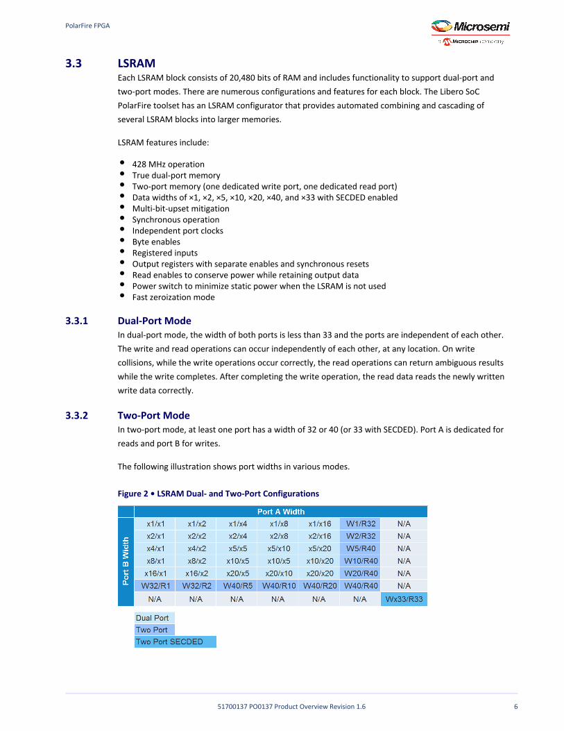
3.3.2 Two-Port ModeIn two-port mode, at least one port has a width of 32 or 40 (or 33 with SECDED). Port A is dedicated for reads and port B for writes.
The following illustration shows port widths in various modes.
Figure 2 • LSRAM Dual- and Two-Port Configurations

PolarFire FPGA
51700137 PO0137 Product Overview Revision 1.6 7
3.4 µSRAMThe µSRAM is a two-port memory embedded in the FPGA fabric, which is provided for an efficient low-power implementation for small buffers. On write collisions, the write operations occur correctly, while the read operations can return ambiguous results while the write completes. After completing the write operation, the read data reads the newly written write data.
The following are key features of the µSRAM block:
480 MHz operationTwo-port memory with 64 words of 12 bitsThe write port operates synchronouslyThe write port has a fixed widthThe read port operates asynchronously and supports synchronous and pipeline operations with the FPGA fabric flip-flopsThe Libero SoC PolarFire toolset provides automated combining and cascading for larger memoriesMultiple memory blocks can be combined to extend the depth or widthProvides a state-keeping, low-power suspend modeImplemented as an array of latches
3.5 µPROMThe µPROM is a single monolithic non-volatile memory that provides a PROM-like storage for a variety of purposes, including but not limited to: initialization data for other memories, user calibration data, and so on. The memory cells are constructed from the FPGA configuration cells and are updated when the device is programmed.
The following are key features of the µPROM:
10 ns read access timeProgrammed with the FPGA bitstreamAsynchronous or synchronous read access mode from the FPGA fabric
3.6 sNVMEach PolarFire FPGA has 56 KBytes of sNVM. The sNVM is organized into 221 pages of 236 or 252 bytes, depending on whether the data is stored as plain text or encrypted/authenticated data. It is accessible to users through system services calls to the PolarFire FPGA system controller. Pages within the sNVM can be marked as ROM during bitstream programming. The sNVM content can be used to initialize LSRAM and µSRAMs with secure data. The sNVM is only accessible through system service calls. Data written to the sNVM can be protected by the PUF.

PolarFire FPGA
51700137 PO0137 Product Overview Revision 1.6 8
3.7 Math BlockThe fundamental building block in any digital signal processing algorithm is the multiply-accumulate (MACC) operation. PolarFire FPGAs implement a custom 18 x 18 MACC block for an efficient low-power implementation of complex DSP algorithms such as finite impulse response (FIR) filters, infinite impulse response (IIR) filters, and fast fourier transform (FFT) for filtering and image processing applications. An optional 16-word coefficient ROM can be constructed from logic elements located near the math block.
The following are key features of the math block functionality:
500 MHz operation18 × 18 two's complement multiplier accumulator with an output width of 48 bitsPower-saving pre-adder to optimize linear phase FIR filter applications and reduce the math block usageOptional pipelining and dedicated buses for cascadingDot-product mode for complex multiplies
The following illustration shows the functional blocks of the math block.
Figure 3 • Math Block

PolarFire FPGA
51700137 PO0137 Product Overview Revision 1.6 9
4 Clock ManagementIn each PolarFire FPGA, there are eight DLLs and eight PLLs to provide flexible clock generation and management capabilities. In addition to these DLLs and PLLs, up to 15 transceiver lane transmit PLLs are also available.
The following are key highlights of the clock management architecture:
High-speed buffers and routing for low-skew clock distributionFrequency synthesis and phase shiftingLow-jitter clock generation and jitter filtering
4.1 DLLThe DLL provides a calculated PVT compensated delay to the I/O’s digital delay lines as well as delay or phase-shifted clocks to the FPGA fabric.
The following are the major modes to which the DLL can be configured.
Time reference mode—the DLL takes a single clock as an input and determines how many delay line buffer taps are required for a signal to pass through them to rotate a signal. The main use of time reference mode is to know how many delay taps are needed to delay the clock by 90 degrees. The value is then provided to the data strobe signal (DQS)/DQSn input signals for double data rate (DDR) memory controllers to delay all DQS/DQSn signals by the required 90-degree phase shift to capture the data from the memory devices. Multiple memory interfaces of the same clock rate can reuse the same DLL with lane level controls for PVT updates.Clock injection delay mode—the DLL can be used to compensate for the clock injection delay associated with the source synchronous receive interfaces. The DLL can match delays for the global, regional, and high-speed bank clocks. There are two outputs from the DLL in this mode: a x1 output fixed in time and another output that can be divided by x1, x2, or x4 and can be phase shifted.
4.2 PLLThe programmable delta-sigma low-jitter fractional PLLs are multi-function and general purpose frequency synthesizers, as shown in the following illustration. Wide input and output ranges along with the best-in-class jitter performance allow these PLLs to be used for almost any clocking application. With excellent supply noise immunity, the PLL is ideal for use in noisy FPGA environments.
The PLL output clock is available in eight phases with 45-degree phase differences. All eight phases are selectable to drive four separate outputs from the PLL, where each output can select any of the eight phases independent of other output selections and that each output can also be driven to a zero output when not used.Each of the four outputs from the PLL can then be divided independently for any value from 1 to 127. Each of the PLL outputs can have the output divider released by up to seven VCO/4 cycles. The delayed outputs can be set independently for each output clock.Fractional-N (24-bit accuracy) capability is added to the feedback divider to have the VCO frequency be a non-integer divide of the reference clock input frequency. The base frequency is applied to all PLL outputs.The PLL supports glitch-free start and stop on any one of the four outputs independently by either a register map or a fabric control. This capability also allows the output divider values and the VCO/4 phase selection to be modified glitch-free during the time that the clock is stopped.
For fine granularity phase control of the PLLs, they can be cascaded with DLLs located near the PLLs,

PolarFire FPGA
51700137 PO0137 Product Overview Revision 1.6 10
For fine granularity phase control of the PLLs, they can be cascaded with DLLs located near the PLLs, whereby the DLL delay lines can be used in a process, voltage, and temperature (PVT) compensated or non-PVT compensated mode to provide the phase control needed.
The following illustration shows the flow of the PLL functionality.
Figure 4 • PLL Block Diagram
4.3 Clock NetworkThe clock network is designed to route clocks and asynchronous reset signals to large sections of the fabric with limited skew. On occasion, the network can also be used for other high fanout signals that can tolerate long delays, such as non-timing-critical synchronous enables or resets. There are two main clock networks for the FPGA fabric, global and regional clocks.
4.3.1 Global ClocksThere are 24 clocks on the device with global low skew scope to all synchronous elements. The global can be divided into left and right sides of the device. Thus, the number of globals can increase to 48 total clocks with 24 in the left and 24 in the right.
4.3.2 Regional ClocksThere are up to 38 regional clock domains that interface to the edges of the device. The regional clocks provide a fixed number of logic elements based on the size of the device. Up to 14 clocks are available for the FPGA I/Os and up to 24 clocks for the transceiver lanes, one for each lane direction. These are the fast insertion clock networks used to move data in and out of the fabric.

PolarFire FPGA
51700137 PO0137 Product Overview Revision 1.6 11
5 I/OsPolarFire device user I/Os support multiple I/O standards while providing the high bandwidth needed to maximize the internal logic capabilities of the device and achieve the required system-level performance.
5.1 Low-Power High-Speed Transceiver LaneAll PolarFire FPGAs contain state-of-the-art low-power transceiver lane capabilities from speeds as low as 250 Mbps up to 12.7 Gbps. The PMA is designed to support multiple protocols (as listed in the following table) with state-of-the-art control and debug features. PCI Express Gen1 or Gen2 support is provided by a hard macro. All other protocols are implemented with a soft IP. Serial Gigabit Ethernet is also supported with GPIO 3.3 V LVDS differential pairs. A single transmit PLL can provide a high-speed clock up to four transceiver lanes.
Table 2 • Transceiver Lane Protocol Support
Protocol Data Rate (Gbps) Channels Bonded
PCIe 2.5, 5 1, 2, 4
Interlaken 6.375, 12.7 1–16
10GBASE-R/KR 10.3125–12.7 1
SGMII/QSGMII 1.25–5 1
XAUI 3.125 4
RXAUI 6.25 2, 3, 4, 6
HiGig/HiGig+/HiGiGII 3.75–4.065 4
CPRI 0.6144–12.165 1
Fiber channel 0.6144–12.165 1
SRIO 1.25–6.3 1, 2, 4, 8
SATA 1.5–6 1
JESD204B 0.5–12.5 1–4
Display port 2, 5, 8 4
SDI 0.277–11.88 1
5.1.1 Low-Power Transceiver Lane FeaturesThe following are low-power transceiver lane features:
Advanced low-power modesProgrammable transmit amplitude and emphasis controlLow-speed CDR operation with support for 270 Mbps SMPTE serial line ratesContinuous time linear equalization (CTLE) and decision feedback equalization (DFE) for long-reach or backplane applicationsAuto-adaption at receiver equalization and integrated eye monitor feature for easy serial link tuningEye monitor and/or equalization can be powered down to reduce power if not neededOut-of-band, electrical idle signaling capability for SAS, SATA, and PCIeMultiple loopback modes for test and debugTransmit jitter attenuation for loop timing applications (SyncE compatible)
Hot-socketing capable

PolarFire FPGA
51700137 PO0137 Product Overview Revision 1.6 12
Hot-socketing capableIEEE 1149.6 AC JTAGAdjacent channel loopback modes allow transceiver lane data streams to remain active during FPGA fabric programming
5.1.2 TransmitterThe transmitter is fundamentally a parallel-to-serial converter with a conversion ratio of 8, 10, 16, 20, 32, 40, 64, or 80 bits. It allows the designer to trade-off data path width for timing margin in high-performance designs. These transmitter outputs drive the PC board with a differential output signal. TX_CLK is the appropriately divided serial data clock available to the fabric, and can be used directly to register the parallel data coming from the internal logic. The transmit parallel data has additional hardware support for the 8b/10b, 64b/66b, or 64b/67b encoding schemes to provide a sufficient number of transitions. The bit-serial output signal drives two package pins with differential signals. The output signal pair supports a wide variety of serial protocols and has programmable signal swing as well as programmable pre- and post-emphasis to compensate for PC board losses and other interconnect characteristics. For shorter channels, the swing can be reduced to lower power consumption. Each transmit lane can be sourced by one of two transmit PLLs. Each transmit PLL can drive up to four transceiver lanes. Transmitter PLLs are state-of-the-art fractional frequency synthesizers with integrated jitter attenuation.
5.1.3 ReceiverThe receiver is fundamentally a serial-to-parallel converter with clock recovery changing the incoming bit-serial differential signal into a parallel stream of words of 8, 10, 16, 20, 32, 40, 64, or 80 bits. This allows the FPGA designer to trade off the internal data path width versus logic timing margin. The receiver takes the incoming differential data stream, feeds it through programmable linear and decision feedback equalizers (to compensate for PC board and other interconnect characteristics), and uses the reference clock input to initiate clock recognition. The data pattern uses non-return-to-zero (NRZ) encoding and optionally guarantees sufficient data transitions by using the selected encoding scheme. The outgoing parallel data has additional hardware support for the 8b/10b, 64b/66b, or 64b/67b encoding schemes to provide a sufficient number of transitions. Parallel data is transferred into the FPGA logic using the recovered clock (RX_CLK).
5.1.4 Transceiver Lane ModesThe transceiver lane supports five different modes of operations:
PMA—direct access to the PMA without any encoding8b/10b—8b/10b encoding/decoding is provided64b/6xb—64b/66b or 64/67b encoding/decoding with gearbox logic is providedPIPE—a PIPE interface supporting both PCIe Gen2 and SATA 3.0PCIe—direct connection to the embedded PCIe Gen2 controller

PolarFire FPGA
51700137 PO0137 Product Overview Revision 1.6 13
The following illustration shows the collaboration of five modes that transceiver lanes support.
Figure 5 • Transceiver Lane Modes
5.1.5 Reference ClockThe reference clock pins allow connections directly with the transceiver lane quads. The reference clock inputs provide flexibility to interface with both single-ended and differential clocks, and can drive up to two independent clocks per transceiver lane quad. These reference clocks can also be sources for the global and regional clock networks in the FPGA fabric of the device.

PolarFire FPGA
51700137 PO0137 Product Overview Revision 1.6 14
The following illustration shows the connectivity between the reference clock and transceiver lane quads.
Figure 6 • Reference Clock
5.1.6 Quad Lane Overlay AssignmentsThe transceiver lane either connects the parallel side of the interface to the PCIe Gen2 controller or to the fabric. The PCIe connections are fixed in the hardware and have a dedicated number of combinations between the two controllers. The fabric interface is used to support the PMA, 8b/10b,64b/6xb, and PIPE modes and have complete flexibility into the fabric connections.
The following table lists the combinations between the PCIe and fabric controllers.
Table 3 • Quad0 Lane Assignments
PCIe_0 Controller Quad0Lane 0
Quad0Lane 1
Quad0Lane 2
Quad0Lane 3
PCIe_1 Controller
x1 PCIe_0 Not available Not available PCIe_1 x1
x1 PCIe_0 Unused PCIe_1 PCIe_1 x2
x2 PCIe_0 PCIe_0 Not available PCIe_1 x1
x2 PCIe_0 PCIe_0 PCIe_1 PCIe_1 x2

PolarFire FPGA
51700137 PO0137 Product Overview Revision 1.6 15
PCIe_0 Controller Quad0Lane 0
Quad0Lane 1
Quad0Lane 2
Quad0Lane 3
PCIe_1 Controller
x4 PCIe_0 PCIe_0 PCIe_0 PCIe_0 Unused
x1 PCIe_0 Not available Fabric Fabric Unused
x2 PCIe_0 PCIe_0 Fabric Fabric Unused
Unused Fabric Fabric Not available PCIe_1 x1
Unused Fabric Fabric PCIe_1 PCIe_1 x2
Unused Fabric Fabric Fabric Fabric Unused
Note: Fabric includes PMA, 8b/10b, 64b/66b, 64b/67b, and PIPE modes.
5.2 Inputs/OutputsPolarFire FPGA I/Os are grouped into pairs to meet the differential I/O standards. Additionally, they are grouped in lanes of 12 buffers with a lane controller for memory interfaces, as shown in the following illustration.
Figure 7 • I/O Topology
The number of I/O pins varies depending on the device and package size. The persistent I/O feature preserves a state on an I/O without user intervention during programming mode. The PolarFire FPGAI/O buffers are constructed from the following main sub modules.
Transmit buffer (PVT compensated)Receive bufferTermination (Thevenin, Differential, Up, and Down)Weak pull mode logic (Up, Down, and Bus-Hold)
Each I/O is configurable and can comply with a large number of I/O standards. Please refer to the PolarFire FPGA datasheet for specific IO standard support and data rates. There two types of userI/Os in PolarFire FPGAs:
High-speed I/O (HSIO) optimized for DDR4 memories at speeds up to 1.6 Gbps and a maximum voltage of 1.8 V nominalGPIO capable of supporting multiple standards including 3.3 V with an integrated CDR to support SGMII Ethernet applications
The following table lists the GPIO LVTTL or LVCMOS receivers that are also designed to support a limited mixed mode of operation to provide greater board I/O design flexibility. For example, if VDDIO is set to 3.3 V, the I/O receivers can operate at the lower voltage of JEDEC standards.

PolarFire FPGA
51700137 PO0137 Product Overview Revision 1.6 16
Table 4 • GPIO Mixed Receiver Mode Operation Capability
VDDIO (V) LVCMOS33 LVCMOS25 LVCMOS18 LVCMOS15 LVCMOS12
3.3 Yes Yes Yes Not available Yes
2.5 Yes Yes Yes Yes Yes
1.8 Yes Yes Yes Yes Yes
1.5 Yes Yes Yes Yes Yes
1.2 Yes Yes Not available Yes Yes
The following table lists the HSIO mixed receiver mode capability.
Table 5 • HSIO Mixed Receiver Mode Capability
VDDIO (V) LVCMOS18 LVCMOS15 LVCMOS12
1.8 Yes Yes Yes
1.5 Yes Yes Yes
1.2 Not available Yes Yes
5.3 I/O DigitalThe PolarFire FPGA I/O digital logic is used to interface between the FPGA fabric and the I/O buffers. It interfaces between the high-speed I/O buffers and lower-speed FPGA fabric. The I/O digital block consists of the following:
A delay chain, for input or output delayRegisters and control logic for input modes and output modes
The I/O digital registers can be configured for both input and output DDR and shift register modes and combined DDR-shift register modes. It allows gearing up the output data rate and gearing down the input data rate. The PolarFire FPGA I/O digital logic works in conjunction with fast and low-skew clock distributions that are optimized for DDR applications, special clock dividers, and other support circuits to guarantee clock domain crossings.
5.3.1 I/O Digital FeaturesThe following are the I/O digital features:
Programmable input and/or output delay chainData eye monitor for detecting margin to clock edgesData eye position optimizerUp to 10:1 input deserializationUp to 10:1 output serializationSupport for DDR and SDR interfacesReceive slip control to facilitate word alignmentFast and low-skew lane clocks per 12 I/OsClock recovery for SGMII and similar interfaces (one per 12 I/Os)

PolarFire FPGA
51700137 PO0137 Product Overview Revision 1.6 17
5.3.2 I/O Digital ModesThe following table lists the associated memory interface, I/O data rate, FPGA clock rate, and its applications.
Table 6 • I/O Digital Modes
Interface Direction I/O Data Rate
I/O Clock Rate(MHz)
Gear Ratio
FPGA Clock Rate(MHz)
Applications
DDR4 BiDir 1.6 Gbps 800 8:1 200 Memory interface
DDR3 (L) BiDir 1.3 Gbps 650 8:1 162.5 Memory interface
LPDDR3 BiDir 1.3 Gbps 650 8:1 162.5 Low-power memory interface
QDRII+ Input/Output
1.1 Gbps 550 8:1 137.5 Low-latency memory interface
RLDRAM3 Input/Output
1.0 Gbps 500 8:1 125 Low-latency memory interface
7:1 LVDS Input 800 Mbps 400 7:1 114 Flatlink, Cameralink
CDR Input 1.25 Gbps 625 10:1 125 1000BASE-T, SGMII
MIPI-DPHY Input/Output
800 Mbps/500 Mbps
250 2:1 125 MIPI CSI, DSI

PolarFire FPGA
51700137 PO0137 Product Overview Revision 1.6 18
6 PCI ExpressEach PolarFire FPGA integrates two low-power built-in PCIe Gen2 controllers, allowing seamless and easy connectivity to one or more host processors. The two PCIe controllers are shared across two quads, as shown in the following illustration. All PLLs are jitter attenuation-capable, while the SSC label indicates spread spectrum clock (SSC) capability.
Figure 8 • PCI Express Hard Macro Lane Sharing

PolarFire FPGA
51700137 PO0137 Product Overview Revision 1.6 19
6.1 PCI Express FeaturesThe following are PCIe features:
×1, ×2, and ×4 lane supportSuitable for root port, native endpointPCI Express base specification revision 2.0 and 1.1 compliantAXI4 master and slave interfaces to the FPGA fabricSingle function capabilityAdvanced error reporting (AER) supportIntegrated clock domain crossing (CDC) to support user-selected AXI4 frequencyLane reversal supportLegacy PCI power management supportNative active state power management L0s and L1 state supportPower management event (PME message)MSI and legacy INT message supportLatency tolerance reporting (LTR)L1 PM sub-states with CLKREQAddress translation tables between the PCIe and AXI4 domains
6.2 PCI Express DMA EnginesEach PCIe controller supports the following built-in DMA modes, enabling low-power and efficient data transfer into the FPGA fabric.
Two DMA channelsEight outstanding read and write requestsCompletion reordering supportFlexible scatter-gather DMA modes, including dynamic DMA control per descriptorOptional DMA engine reporting to the descriptor to ease software managementFetching of up to three descriptors to optimize throughput

PolarFire FPGA
51700137 PO0137 Product Overview Revision 1.6 20
7 PolarFire FPGA System ControllerThe PolarFire FPGA system controller is based on the industry-standard ARM Cortex-M3 and is only used for FPGA powerup, secure DPA safe FPGA programming, and executing and responding to system services. All internal memories are SECDED protected with background scrubbing capabilities to remove single bit errors.
7.1 System ServicesSystem services provide the user with information about the state of the FPGA and allow the user to request the system controller to perform predefined functions using a standard Application Programming Interface (API).
Design services
Initialize fabric RAMBitstream authenticationIAP image authentication
Data services
sNVM read/writePUF emulation serviceNonce service
Device services
Serial numberJTAG user codeDesign version numberDevice certificate
FPGA fabric services
In-application programmingDigest check

PolarFire FPGA
51700137 PO0137 Product Overview Revision 1.6 21
8 Debug Probe SystemTwo specified user I/Os can be configured (at design capture stage) as either two single-ended live probes or one differential live probe. These live probes can provide read access to any register in the FPGA fabric, to the output pipeline registers in the LSRAMs, and to all the registers in the math block in real-time without having to re-instrument the code. A snapshot of all internal probe points can be created and read out asynchronously. The live-probe feature can be considered like a two-channel oscilloscope, whose two channels can be routed out to I/Os for external observation, and to internal ports to allow fabric design observation. Selecting different probe points within the PolarFire FPGA occurs dynamically through commands over the JTAG port using SmartDebug. Reprogramming of the FPGA is not required.
The debug probe system includes the following:
Active probe allows dynamic asynchronous read and write to a flip-flop or a probe point. This enables quick internal observation of the logic output or experimentation on how the logic will be affected by writing to a probe point.Memory debug allows dynamic asynchronous read and write to a µSRAM or a large SRAM block to quickly verify if the content of the memory is changing as expected.Probe insertion allows routing of nodes or debug points in the FPGA design externally through unused I/Os. An oscilloscope/logic analyzer can be attached to monitor them as live signals.
PolarFire FPGA
51700137 PO0137 Product Overview Revision 1.6 22
9 ProgrammingMicrosemi’s PolarFire FPGAs have multiple programming modes designed to enable various use models. All bitstreams are always encrypted and DPA safe. Each PolarFire FPGA can be programmed using a dedicated SPI peripheral and JTAG port. All PolarFire FPGAs are typically reprogrammed in less than 60 seconds. For device specific programming timings, see .DS0141: PolarFire FPGA Datasheet
The following programming modes are supported:
Slave Programming
JTAGSlave SPI—an external SPI master programs the FPGA
SPI Master Programming—In-Application Programming (IAP)
Auto update feature—the system controller on power-up checks for a new bitstream in an external SPI flash and programs the FPGA.Auto programming feature—on a blank device, the system controller on power-up checks for a bitstream in an external SPI flash and programs the FPGA.Programming recovery feature—if remote programming fails due to a power interruption, the system controller reprograms the FPGA on the next power-up cycle from a golden bitstream (located in an external SPI flash).
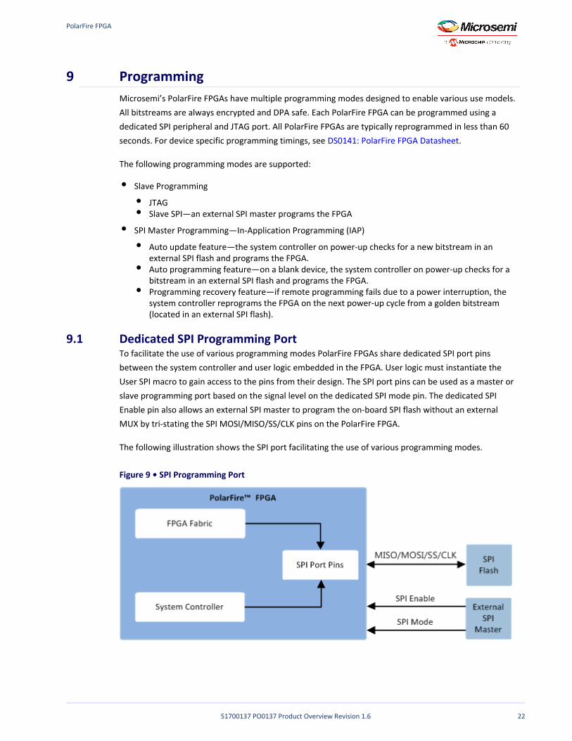
9.1 Dedicated SPI Programming PortTo facilitate the use of various programming modes PolarFire FPGAs share dedicated SPI port pins between the system controller and user logic embedded in the FPGA. User logic must instantiate the User SPI macro to gain access to the pins from their design. The SPI port pins can be used as a master or slave programming port based on the signal level on the dedicated SPI mode pin. The dedicated SPI Enable pin also allows an external SPI master to program the on-board SPI flash without an external MUX by tri-stating the SPI MOSI/MISO/SS/CLK pins on the PolarFire FPGA.
The following illustration shows the SPI port facilitating the use of various programming modes.
Figure 9 • SPI Programming Port
PolarFire FPGA
51700137 PO0137 Product Overview Revision 1.6 23
10 Low PowerPolarFire FPGAs offer a variety of techniques and capabilities to lower the total application power. Users can take advantage of these features to lower both capital and operational expenditures with smaller or no heat sinks, smaller or fewer fans, lower cooling costs, and so on. Additionally, the lower total power advantage can also allow the user to pack more compute operations into an existing thermal budget.
10.1 Non-Volatile TechnologyUsing a non-volatile complementary metal–oxide semiconductor (CMOS) technology for the FPGA configuration cells offers several power advantages over SRAM FPGA technology.
A non-volatile switch has lower power than a SRAM switch, leading to lower static power consumptionNo SRAM configuration in-rush currentsAn external configuration component is not necessary
10.2 Low-Power Transceiver LanePolarFire FPGAs’ low-power capability is also extended to the industry’s most power efficient transceiver lane, enabling 10GBASE-KR applications at less than 100 mW of power per lane. The transceiver lane has comprehensive power-down controls to optimize power consumption, including programmable amplitude and edge rate control.
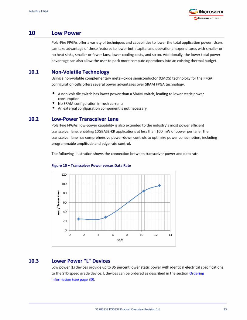
The following illustration shows the connection between transceiver power and data rate.
Figure 10 • Transceiver Power versus Data Rate
10.3 Lower Power "L" DevicesLow power (L) devices provide up to 35 percent lower static power with identical electrical specifications to the STD speed grade device. L devices can be ordered as described in the section Ordering
.Information (see page 30)

PolarFire FPGA
51700137 PO0137 Product Overview Revision 1.6 24
11 ReliabilityMicrosemi continues to offer the industry’s most reliable FPGAs for your mission and safety critical applications.
11.1 FPGA FabricPolarFire FPGA configuration cells are inherently immune to SEUs caused by neutrons. Contrary to popular belief, shielding does not prevent a neutron from passing through an electronic system or electronic device. As semiconductor device geometry shrinks to smaller lithography, the problem of MBUs starts appearing. SRAM FPGA scrubbing techniques might be inadequate in these circumstances and while scrubbing may help, an important point is that scrubbing detects an error after the fact. The error has already occurred and propagated throughout the system. The configuration of the PolarFire FPGA fabric provides worry-free operation against random events caused by SEUs.
11.2 LSRAMLSRAMs have built-in SECDED capability on a 32-bit word boundary. Seven additional bits are used for error correction. Two flags are provided to the user to indicate SECDED. Mitigation against multi-bit upsets is provided by keeping all cells in a word separated by a minimum distance. Applications that require scrubbing need to be accomplished with user logic. The error correction logic can be turned ON and OFF by the user to enable easy validation of the error correction operation.
11.3 µSRAMThe 64 × 12 µSRAMs are constructed from latches and are not as sensitive to SEUs as SRAMs are.
11.4 DigestsDigests verify the integrity of the programmed non-volatile data. Digests are a cryptographic hash of various data areas. Any digest that reports back an error raises the digest tamper flag.
The following are digestible non-volatile areas:
The FPGA fabric and consequently the µPROMsNVM marked as ROMUser key 1User key 2Factory parametric and key storage
PolarFire FPGA
51700137 PO0137 Product Overview Revision 1.6 25
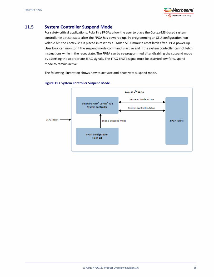
11.5 System Controller Suspend ModeFor safety critical applications, PolarFire FPGAs allow the user to place the Cortex-M3-based system controller in a reset state after the FPGA has powered up. By programming an SEU configuration non-volatile bit, the Cortex-M3 is placed in reset by a TMRed SEU immune reset latch after FPGA power-up. User logic can monitor if the suspend mode command is active and if the system controller cannot fetch instructions while in the reset state. The FPGA can be re-programmed after disabling the suspend mode by asserting the appropriate JTAG signals. The JTAG TRSTB signal must be asserted low for suspend mode to remain active.
The following illustration shows how to activate and deactivate suspend mode.
Figure 11 • System Controller Suspend Mode

PolarFire FPGA
51700137 PO0137 Product Overview Revision 1.6 26
12 SecurityToday’s demanding applications not only have to meet the functional requirements, but also to meet them in a secured way. Security starts during silicon manufacturing and continues through system deployment and operations. Microsemi’s PolarFire FPGAs represent the industry’s most advanced secure programmable FPGAs.
12.1 Design SecurityProtecting your design starts with wafer manufacturing and continues through the deployment of the end product. The following are key features that provide state-of-the-art supply chain assurance and IP protection benefits in all PolarFire FPGA devices:
Secure supply chain management through the use of hardware security modules (HSMs) during wafer test and packagingSupply chain assurance through the use of a 768-byte digitally signed x.509 FPGA certificate embedded in every FPGAAES256-encrypted CRI DPA countermeasures patent protected, bitstream, and key management protocolsBuilt-in tamper detectors: voltage monitors, temperature monitor, clock glitch detectors, voltage glitch detectors, protective meshes, and bus scramblingData integrity through built-in cryptographic digest capabilitiesZeroization capabilities for all on-chip memories and the FPGA fabricIntegrated PUF for the ultimate in key storage56 Kbytes of PUF protected sNVM
Secure reprogrammable keys using non-volatile memory
12.1.1 Tamper DetectorsMicrosemi’s PolarFire FPGAs integrate numerous on-chip tamper detectors, enabling users to monitor the environment and the operating parameters of the design. The user can respond to the events that are determined to be out-of-scope for proper operation. Tamper flags indicate that a tamper event has occurred and are available as signals to the FPGA fabric for users to process and respond. The following is a partial list of tamper detectors:
Clock glitch detectorsClock frequency detectorsVoltage monitor detectorsTemperature sensorJTAG active detectorMesh active detector
12.1.2 Tamper ResponsesAfter processing a detected event, the user can perform one of the following actions.
Disable I/Os—configurable on a per I/O basisSecurity lockdownResetZeroize

PolarFire FPGA
51700137 PO0137 Product Overview Revision 1.6 27
12.2 Data SecuritySelect Microsemi PolarFire FPGAs (TS FPGAs) build on the design security capabilities in all PolarFire FPGAs by enabling high-speed DPA safe cryptographic protocols at wire-line speeds. PolarFire data security FPGAs include the following additional features.
Integrated true random number generator for enabling modern cryptographic protocols capable of generating random numbers at greater than 100 Mbps189 MHz Athena TeraFire 5200B DPA safe Crypto Coprocessor capable of implementing Suite-B+ algorithmsCRI DPA pass-through licensing enabling DPA safe high-speed cryptographic designs in the FPGA fabric. A CRI license is included in the purchase price of the TS FPGA. There is no need to negotiate a separate license.NIST-certified protocols
The following are TeraFire EXP-F5200B supported protocols/features:
TRNG (integrated): SP800-90A CTR_DRBG-256, and SP800-90B(draft) NRBGAES-128/192/256 E/D (ECB, CBC, CTR, OFB, CFB, CCM, GCM, KeyWrap)
AES GCM mode is implemented through an application note.Note:
SHA-1/224/256/384/512HMAC-SHA-256/384/512; GMAC; CMACSHA-256 Key TreeECC-NIST P192/224/256/384/521 and Brainpool P256/384/512 curves with: KAS-ECC CDH; ECDSA-SigGen, SigVer, PKG, and PKVFFC: 1024/1536/2048/3072/4096-bits with: DSA SigGen and SigVer; and KAS-DHIFC: 1024/1536/2048/3072/4096/8192-bits with: RSA E/D; SSA_PKCS1_V1_5 SigGen and SigVer; and ANSI X9.31 SigGen and SigVer
PolarFire FPGA
51700137 PO0137 Product Overview Revision 1.6 28
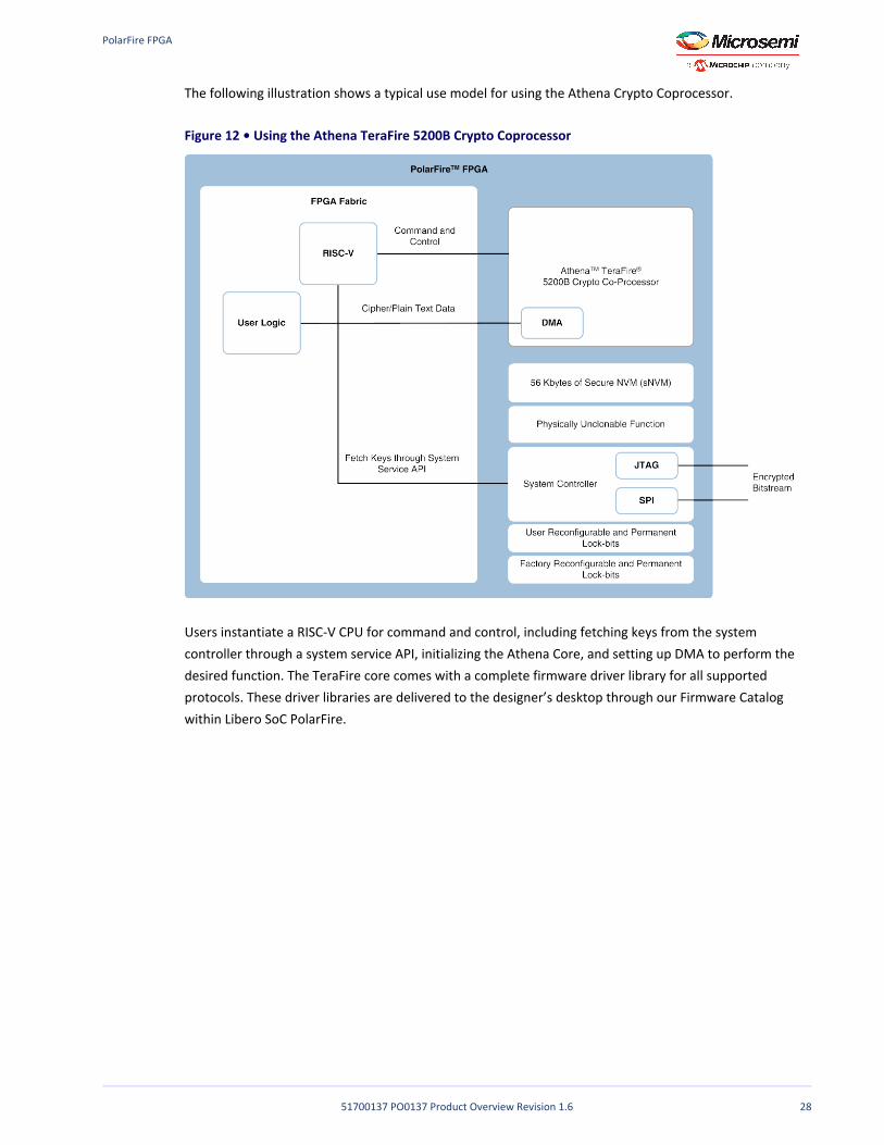
The following illustration shows a typical use model for using the Athena Crypto Coprocessor.
Figure 12 • Using the Athena TeraFire 5200B Crypto Coprocessor
Users instantiate a RISC-V CPU for command and control, including fetching keys from the system controller through a system service API, initializing the Athena Core, and setting up DMA to perform the desired function. The TeraFire core comes with a complete firmware driver library for all supported protocols. These driver libraries are delivered to the designer’s desktop through our Firmware Catalog within Libero SoC PolarFire.

PolarFire FPGA
51700137 PO0137 Product Overview Revision 1.6 29
13 PolarFire FPGA Device OfferingsPolarFire FPGAs offer low-power transceiver devices and various device offerings with transceivers, such as design security, data security, and low-power data security. All PolarFire FPGAs are integrated with multi-protocol industry-leading low-power transceivers. Low power (L) devices provide up to 35 percent lower static power with identical electrical specifications to the STD speed grade device. Also, data security (S) devices integrate a DPA-resistant crypto accelerator.
The following table lists the PolarFire FPGA device options using the MPF300T as an example. The MPF100T, MPF200T, and MPF500T device densities have identical offerings. Temperatures listed are junction temperatures.
Table 7 • PolarFire FPGA Offerings
DeviceOptions
Extended Commercial Temperature (E)0 °C–100 °C
Industrial Temperature (I)–40 °C–100 °C
STDSpeedGrade
–1SpeedGrade
Transceivers (T)
Lower Static Power (L)
Data Security (S)
MPF300T Yes Yes Yes Yes Yes
MPF300TL Yes Yes Yes Yes Yes
MPF300TS Yes Yes Yes Yes Yes
MPF300TLS Yes Yes Yes Yes Yes
The following table lists the planned military temperature offerings for the PolarFire FPGA device (data security "S", STD speed grade, leaded package, –55 °C–125 °C Tj). For availability, please contact your local Microsemi representative. Only Military Temperature grade devices are offered in a leaded package.
Table 8 • PolarFire FPGA Military Temperature Offering
Package Type MPF200TS MPF300TS MPF500TS
FCS325 (11x14.5, 0.5 mm) Yes
FCS536 (16x16, 0.5 mm) Yes
FCV484 (19x19, 0.8 mm) Yes
FC484 (23x23, 1.0 mm) Yes
FC784 (29x29, 1.0 mm) Yes
FC1152 (35x35, 1.0 mm) Yes

PolarFire FPGA
51700137 PO0137 Product Overview Revision 1.6 30
14 Ordering InformationPolarFire FPGAs are offered with multiple speed grades, temperatures, and package combinations. All FPGAs are equipped with low-power transceivers. All temperatures are specified as junction temperatures.
Figure 13 • Ordering Information

PolarFire FPGA
51700137 PO0137 Product Overview Revision 1.6 31
15 Export Classification
The following table lists the PolarFire FPGA export classification using the MPF300T as an example. The MPF100T, MPF200T, and MPF500T device densities have identical classifications. This table is applicable to extended commercial and industrial temperature grade devices.
Table 9 • PolarFire FPGA Export Classification
DeviceOptions
Data Security (S) ECCN
MPF300T No 3A991.d
MPF300TL No 3A991.d
MPF300TS Yes 5A002.a.1
MPF300TLS Yes 5A002.a.1

PolarFire FPGA
51700137 PO0137 Product Overview Revision 1.6 32
Microsemi HeadquartersOne Enterprise, Aliso Viejo,CA 92656 USAWithin the USA: +1 (800) 713-4113Outside the USA: +1 (949) 380-6100Sales: +1 (949) 380-6136Fax: +1 (949) 215-4996Email: [email protected]
© 2017-2019 Microsemi. All rights reserved. Microsemi and the Microsemi logo are trademarks of Microsemi Corporation. All other trademarks and service marks are the property of their respective owners.
Microsemi makes no warranty, representation, or guarantee regarding the information contained herein or the suitability of its products and services for any particular purpose, nor does Microsemi assume any liability whatsoever arising out of the application or use of any product or circuit. The products sold hereunder and any other products sold by Microsemi have been subject to limited testing and should not be used in conjunction with mission-critical equipment or applications. Any performance specifications are believed to be reliable but are not verified, and Buyer must conduct and complete all performance and other testing of the products, alone and together with, or installed in, any end-products. Buyer shall not rely on any data and performance specifications or parameters provided by Microsemi. It is the Buyer's responsibility to independently determine suitability of any products and to test and verify the same. The information provided by Microsemi hereunder is provided "as is, where is" and with all faults, and the entire risk associated with such information is entirely with the Buyer. Microsemi does not grant, explicitly or implicitly, to any party any patent rights, licenses, or any other IP rights, whether with regard to such information itself or anything described by such information. Information provided in this document is proprietary to Microsemi, and Microsemi reserves the right to make any changes to the information in this document or to any products and services at any time without notice.
Microsemi, a wholly owned subsidiary of Microchip Technology Inc. (Nasdaq: MCHP), offers a comprehensive portfolio of semiconductor and system solutions for aerospace & defense, communications, data center and industrial markets. Products include high-performance and radiation-hardened analog mixed-signal integrated circuits, FPGAs, SoCs and ASICs; power management products; timing and synchronization devices and precise time solutions, setting the world's standard for time; voice processing devices; RF solutions; discrete components; enterprise storage and communication solutions; security technologies and scalable anti-tamper products; Ethernet solutions; Power-over-Ethernet ICs and midspans; as well as custom design capabilities and services. Microsemi is headquartered in Aliso Viejo, California, and has approximately 4,800 employees globally. Learn more at www.microsemi.com.
51700137