Embed Size (px)
Citation preview

©On-Bright Electronics Confidential
OB_DOC_ DBM _2358A2 -1-
12W Adapter Module Using OB2358 AD12V1A2358.00
Subject
OB2358 Demo Board Manual Board Model: AD12V1A2358.00
Doc. No.: OB_DOC_DBM_2358A2
Key features:
Standby Power < 0.30W
Soft start to relax external component rating
requirement
OCP with line compensation
Frequency shuffling technology for improved EMI
performance
OCP/OVP/OLP/ SCP Protection Features
Audio noise free operation
Passed EN55022 Class B & FCC Part Class B
Revision History
Revise Date Version Reason/Issue
2007-09-28 A0 First issue
2008-03-03 A1 Update schematic, Bill of material
2008-05-22 A2 Update Bill of material(LF1 or Cancel)and EMI report
Page10:CEC test report in Lin END.
On-Brig
ht C
onfid
entia
l To
MMC
©On-Bright Electronics Confidential
OB_DOC_ DBM _2358A2 -2-
12W Adapter Module Using OB2358 AD12V1A2358.00
Contents Index 1. Adapter Module Specification ...................................................................................................4
1.1. Input Characteristics .........................................................................................................4 1.2. Output Characteristics.......................................................................................................4 1.3. Performance Specifications...............................................................................................4 1.4. Protection Features...........................................................................................................4 1.5. Environments ....................................................................................................................4
2. Adapter Module Information......................................................................................................5 2.1. Schematic .........................................................................................................................5 2.2. Bill of material....................................................................................................................5 2.3. PCB Gerber File................................................................................................................7 2.4. Adapter Module Snapshot.................................................................................................7 2.5. Transformer design ...........................................................................................................8 2.5.1. Transformer Specification ..................................................................................................8 2.5.2. Structure/Material...............................................................................................................8
3. Performance Evaluation ............................................................................................................9 3.1. Input Characteristics .......................................................................................................10 3.1.1. Standby power .................................................................................................................10 3.1.2. Efficiency .........................................................................................................................10 3.2. Output Characteristics.....................................................................................................10 3.2.1. Line Regulation & Load Regulation .................................................................................10 3.2.2. Ripple & Noise.................................................................................................................10 3.2.3. Over shoot & Under shoot ............................................................................................... 11 3.2.4. Dynamic Test ...................................................................................................................12 3.2.5. Time Sequence ( Full load)..............................................................................................13 3.3. EMI Test ..........................................................................................................................15 3.3.1. Conducted EMI Test ........................................................................................................15 3.3.1.1 EN55022 CLASS B @ full load report ............................................................................15 3.3.1.2 FCC CLASS B @ full load report....................................................................................15 3.3.2. Radiation EMI Test...........................................................................................................16 3.3.2.1.EN55022 CLASS B @ full load report ............................................................................16 3.3.2.2.FCC CLASS B @ full load report....................................................................................16
4. Protection..................................................................................................................................19 4.1. Over voltage protection ...................................................................................................19 4.2. Short circuit protection ....................................................................................................19 4.3. Over Loop Protection ......................................................................................................19
5. Thermal Testing........................................................................................................................20 6. Other important waveform.......................................................................................................21
6.1. Vdd, Sense& FB&Vds wave form @ no load /full load ....................................................21 6.2. MOSFET Vds waveform @ start/normal/output short .....................................................21
On-Brig
ht C
onfid
entia
l To
MMC

©On-Bright Electronics Confidential
OB_DOC_ DBM _2358A2 -3-
12W Adapter Module Using OB2358 AD12V1A2358.00
Figures Index Fig. 1 Measured ripple& noise waveform@90Vac/60HZ, no load. .................................................. 11 Fig. 2 Measured ripple& noise waveform@90Vac/60HZ, full load. ................................................. 11 Fig. 3 Measured ripple& noise waveform@264Vac/50HZ, no load................................................. 11 Fig. 4 Measured ripple& noise waveform@264Vac/50HZ, full load ................................................ 11 Fig. 5 Measured overshoot waveform@90Vac/60HZ, full load .......................................................12 Fig. 6 Measured overshoot waveform@90Vac/60HZ, no load........................................................12 Fig. 7 Measured overshoot waveform@264Vac/50HZ, full load........................................................12 Fig. 8 Measured overshoot waveform@264Vac/50HZ, no load......................................................12 Fig. 9 Output voltage waveform under Dynamic test @264Vac/50HZ ............................................13 Fig. 10 Output voltage waveform under Dynamic test@90Vac/60HZ .............................................13 Fig. 11 Turn on delay time measured waveform@100Vac/60HZ,full load.......................................13 Fig. 12 Turn on delay time measured waveform@240Vac/50HZ,full load.......................................13 Fig. 13 Hold-up time measured waveform@100Vac/60HZ,full load................................................14 Fig. 14 Rise time measured waveform@100Vac/60HZ,full load .....................................................14 Fig. 15 Rise time measured waveform@240Vac/50HZ,full load .....................................................14 Fig. 16 Fall time measured waveform@100Vac/60HZ,full load ......................................................14 Fig. 17 Fall time measured waveform@240Vac/50HZ,full load ......................................................14 Fig. 18 Output short, Vds waveform@264 Vac/50Hz, full load .......................................................19 Fig. 19 Vdd, Sense&FB&Vds waveform@90Vac/60Hz, ,full load ...................................................21 Fig. 20 Vdd,Sense &FB&Vds waveform @264Vac/50Hz, full load....................................................21 Fig. 21 Start, Vds waveform@90 Vac/60Hz, full load......................................................................21 Fig. 22 Start, Vds waveform@264 Vac/50Hz, full load....................................................................21 Fig. 23 Normal, Vds waveform@264 Vac/50Hz, full load................................................................21 Fig. 24 Output short, Vds waveform@264 Vac/50Hz,.....................................................................21
Tables Index Table. 1 Standby power...................................................................................................................10 Table. 2 Efficiency ...........................................................................................................................10 Table. 3 Line Regulation & Load Regulation ...................................................................................10 Table. 4 Ripple & Noise...................................................................................................................10 Table. 5 Over shoot & Under shoot measurement results............................................................... 11 Table. 6 Output voltage under dynamic test ....................................................................................12 Table. 7 Turn-on delay/hold-up/rise/fall time measurement results .................................................13 Table. 8 OVP @ no load..................................................................................................................19 Table. 9 OLP @ Full load ................................................................................................................19 Table. 10 Vds_max @ Full load / Output short................................................................................22
On-Brig
ht C
onfid
entia
l To
MMC

©On-Bright Electronics Confidential
OB_DOC_ DBM _2358A2 -4-
12W Adapter Module Using OB2358 AD12V1A2358.00
1. Adapter Module Specification
1.1. Input Characteristics
AC input voltage rating 100Vac ~ 240Vac
AC input voltage range 90Vac ~ 264Vac
AC input frequency range 47Hz ~ 63Hz
1.2. Output Characteristics Output Voltage 12V
Output Tolerance 5%
Min. load current 0A
Max. load current 1.0A
1.3. Performance Specifications Max. Output Power 12W
Standby Power <0.3W @ 264V/50Hz, no load, 25°C
Efficiency >75% @Ave. 25/50/75/100%Load, normal line, 25°C
Line Regulation 1% Max
Load Regulation 5% Max
Ripple & Noise 100 mV Max
Hold up Time 10m Sec. Min. @100Vac with full load
Turn on Delay Time 2 Sec. Max. @100Vac with full load
1.4. Protection Features Short circuit Protection Output shut down with automatic recovery
Over Voltage Protection Output shut down with automatic recovery
Over Load Protection Output shut down with automatic recovery
1.5. Environments Operating Temperature 0 to +40
Operating Humidity 20% to 90% R.H.
Storage Temperature -40 to +60
Storage Humidity 0% to 95% R.H.
On-Brig
ht C
onfid
entia
l To
MMC

©On-Bright Electronics Confidential
OB_DOC_ DBM _2358A2 -5-
12W Adapter Module Using OB2358 AD12V1A2358.00
2. Adapter Module Information
2.1.Schematic
2.2.Bill of material No. Position Description Quantity Remark1 L,N IEC-6 2Pin Socket 1 2 V+,V- Output cable 22AWG 1.2M 1 3 F1 FUSE,T1AH/250V 1 4 MOV1 MOVR 07D471K 1 5 T1 Transformer EF20 132:18:23 2.4mH 1
6 LF1 Filter;od:6.1/id:2.8/h:3.3 Ф0.45*2/9T, L=180uH Min Or N.C. (Or Cancel---JUMP 2pcs)
1
7 L1 Chock, DR6*8, Ф0.20x170T,600uH MIN 1 8 L2 Chock,Ф0.7x10.5T,1.7uH MIN 1 9 L3 Bead core(gap):Ф0.25x4T 1
10 C1,C2 E.C 10uF 400V 2 12 C3 C.C 222P 1KV DIP 1 12 C4 E.C 10uF 50V DIP 1 13 C5 SMD 360pF 50V 0805 1 14 C6 SMD 10nF 50V 0805 1 15 C8 SMD 102P 50V 0805 1 16 C9,C10 E.C 470uF 16V Low ESR 2 17 C12 SMD 22nF 50V 0805 1 18 R1,R2 SMD 1M 5% 1206 2
On-Brig
ht C
onfid
entia
l To
MMC

©On-Bright Electronics Confidential
OB_DOC_ DBM _2358A2 -6-
12W Adapter Module Using OB2358 AD12V1A2358.00
19 R3 CFR 100K 5% 1W 1 20 R4 SMD 62Ω 5% 0805 1 21 R5 SMD 5Ω1 5% 0805 1 22 R6 SMD 1K 5% 0805 1 23 R7 CFR 1.5Ω 5% 1W 1 24 R19 SMD 10Ω 5% 1206 1 25 R9 SMD 10Ω 5% 0805 1 26 R10 SMD 270Ω 5% 1206 1 27 R11 SMD 39K 5% 0805 1 28 R12 SMD 2K 5% 0805 1 29 R13,R14 SMD 10K 5% 0805 2 30 R17 SMD 0R 5% 1206 1 31 R18 SMD 2.4K 5% 1206 1 32 R8,R15,R16,C11,Z2 NC 0 31 D1-D6 Diode 1N4007 6 32 D7 SB diode SB3100(for D7 bead core) 1 33 U1 PWM OB2358 DIP 1 34 U2 Photo coupler 817C 1 35 U3 TL431 1 36 NTC,JMP1 JUMP 2 37 J1 SMD 0R 5% 0805 1 38 PCB OBPD12W-58L120A A1 FR-4, 1
On-Brig
ht C
onfid
entia
l To
MMC

©On-Bright Electronics Confidential
OB_DOC_ DBM _2358A2 -7-
12W Adapter Module Using OB2358 AD12V1A2358.00
2.3.PCB Gerber File
Top
Bottom Copper
2.4.Adapter Module Snapshot
Heat sink
On-Brig
ht C
onfid
entia
l To
MMC

©On-Bright Electronics Confidential
OB_DOC_ DBM _2358A2 -8-
12W Adapter Module Using OB2358 AD12V1A2358.00
2.5.Transformer design
2.5.1. Transformer Specification 1) Bobbin: EF20 (8Pin)
2) Core material: PC40 (TDK).
3) L(2-4) = 2.4mH+/-3% (10KHz,1V,25)
2.5.2. Structure/Material
Winging Material Start Turns Finish COPPER W=12mm 4
TAPE TAPE W=12mm (Y) 1 N1 0.23Φ*1 2UEW 2 44 C
TAPE TAPE W=12mm (Y) 1 N2 0.23Φ*1 2UEW C 44 D
TAPE TAPE W=12mm (Y) 1 N3 0.23Φ*1 2UEW D 44 4
TAPE TAPE W=12mm (Y) 2 COPPER W=12mm 4
TAPE TAPE W=12mm (Y) 3 N4 0.45Φ*1 三层绝缘线 A 18 B
TAPE TAPE W=12mm (Y) 1 N5 0.21Φ*2 2UEW 1 23 3
TAPE TAPE W=12mm (Y) 2 On-
Bright
Con
fiden
tial T
o MMC

©On-Bright Electronics Confidential
OB_DOC_ DBM _2358A2 -9-
12W Adapter Module Using OB2358 AD12V1A2358.00
3. Performance Evaluation This session presents the test results of OBPD12W module up to date. Results on inrush current and safety test are not included and will be added when they become available. Overall, the module meets design specifications. All data was measured at board Lin(AWG22# 1.5m)end. Performance Highlights
The standby power is about 0.23W @ 264Vac/50HZ no load. The average efficiency more than 75% @25/50/75/100% load, normal line. EMI passed EN55022 and FCC15 Class B test with more than 6dB margin.
Characterization Results Summary
Test Item Test result 1. Input characteristics
Input current (90V/60Hz, full load) 0.32A Max Standby power at no load (264Vac,) 0.23W Average Efficiency (264Vac, 25%/50%/75%/100%) 80%
2 .Output characteristics Line regulation 1% Load regulation 5% Ripple & noise 100mV Max Over shoot 5% Max Under shoot Dynamic test 415mV
3. Time sequence (100Vac with Full load) Turn on delay time 907.7mS Hold up time 23.33mS Rise time 7.90mS Fall time 11.20mS
Test Equipments
Item Vender Module AC Source WEST WEW1010
Digital Power Meter YOKOGAWA WT210
Electrical Load Prodigit 3315C
Oscilloscope LeCroy WS424
Multimeter VICTORY VC9807A
On-Brig
ht C
onfid
entia
l To
MMC

©On-Bright Electronics Confidential
OB_DOC_ DBM _2358A2 -10-
12W Adapter Module Using OB2358 AD12V1A2358.00
3.1. Input Characteristics
3.1.1. Standby power
Table. 1 Standby power Input voltage Pin(mW) Vo(V) Specification Test result90Vac/60HZ 100 12.19115Vac/60HZ 130 12.19230Vac/50HZ 190 12.19264Vac/50HZ 228 12.19
<300mW Pass
3.1.2. Efficiency Table. 2 Efficiency
Input voltage 25% 50% 75% 100% Aver. Eff. EPS2.090Vac/60HZ 79.49 80.60 80.26 79.42 79.94 115Vac/60HZ 78.48 81.65 81.55 80.61 80.57 230Vac/50HZ 74.41 79.07 80.67 80.40 78.64 264Vac/50HZ 73.55 78.17 79.38 79.09 77.55
>77.76%
3.2.Output Characteristics
3.2.1. Line Regulation & Load Regulation Table. 3 Line Regulation & Load Regulation
Input voltage No load Half load Full load Specification Test
result 90Vac/60HZ 12.186 12.156 12.138 115Vac/60HZ 12.186 12.156 12.138 230Vac/50HZ 12.186 12.156 12.138 264Vac/50HZ 12.186 12.156 12.138
Line Regulation 0.000% <1% Load Regulation 0.001% <5%
3.2.2. Ripple & Noise Table. 4 Ripple & Noise
R&N (mV) Input voltage
No load Full load Remark 90Vac/60HZ 11.9mV 38mV Fig. 1,2
115Vac/60HZ 11.2mV 42mV
180Vac/50HZ 13mV 35mV
264Vac/50HZ 13mV 36mV Fig. 3,4
Note: Ripple& noise was measured at board end without probe cap and ground clip. Measurement bandwidth was limited to 20MHZ.
On-Brig
ht C
onfid
entia
l To
MMC

©On-Bright Electronics Confidential
OB_DOC_ DBM _2358A2 -11-
12W Adapter Module Using OB2358 AD12V1A2358.00
Fig. 1 Measured ripple& noise waveform@90Vac/60HZ, no load. Fig. 2 Measured ripple& noise waveform@90Vac/60HZ, full load.
Fig. 3 Measured ripple& noise waveform@264Vac/50HZ, no load Fig. 4 Measured ripple& noise waveform@264Vac/50HZ, full load
3.2.3.Over shoot & Under shoot Over shoot and under shoot were measured under below conditions. a. AC input switch on for over shoot and off for under shoot. b. Input voltage ranges from 90Vac/60HZ~264Vac/50HZ. Table. 5 Over shoot & Under shoot measurement results
Input load Remark over shoot Fig. 5
Full load under shoot over shoot Fig. 6
90V/60HZ No load
under shoot over shoot Fig. 7
Full load under shoot over shoot Fig. 8
264V/50HZ No load
under shoot
On-Brig
ht C
onfid
entia
l To
MMC
©On-Bright Electronics Confidential
OB_DOC_ DBM _2358A2 -12-
12W Adapter Module Using OB2358 AD12V1A2358.00
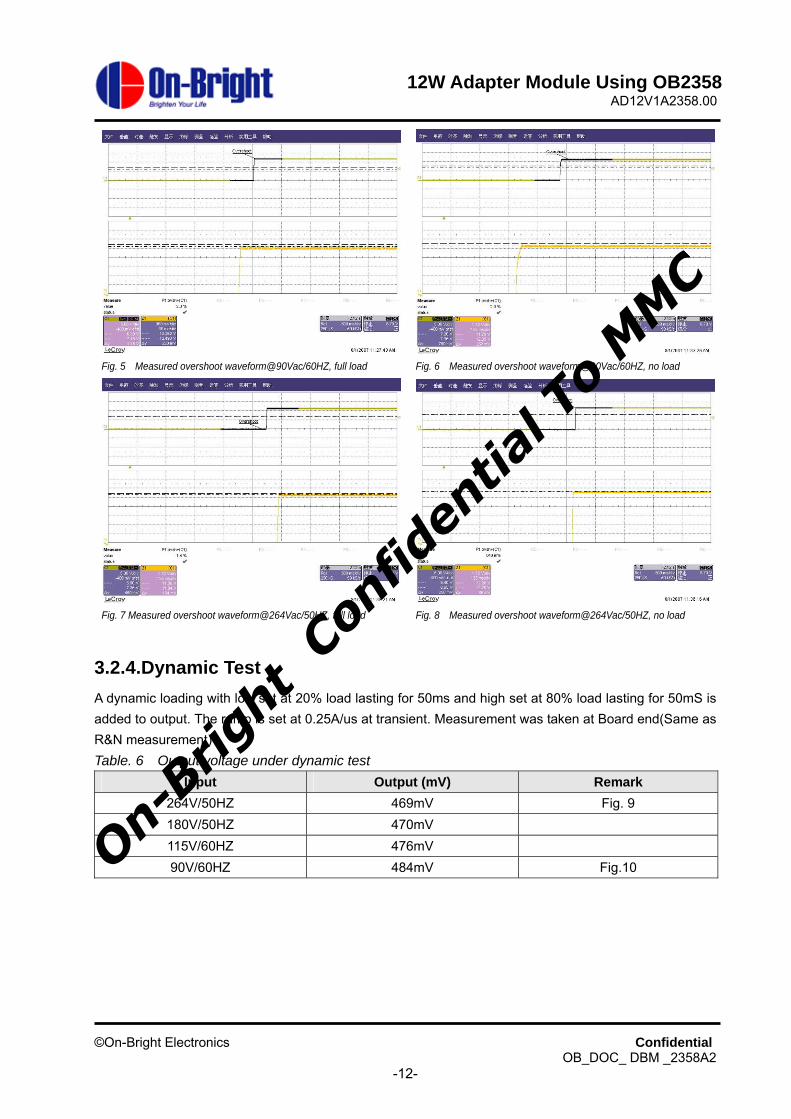
Fig. 5 Measured overshoot waveform@90Vac/60HZ, full load Fig. 6 Measured overshoot waveform@90Vac/60HZ, no load
Fig. 7 Measured overshoot waveform@264Vac/50HZ, full load Fig. 8 Measured overshoot waveform@264Vac/50HZ, no load
3.2.4.Dynamic Test A dynamic loading with low set at 20% load lasting for 50ms and high set at 80% load lasting for 50mS is added to output. The ramp is set at 0.25A/us at transient. Measurement was taken at Board end(Same as R&N measurement) Table. 6 Output voltage under dynamic test
Input Output (mV) Remark 264V/50HZ 469mV Fig. 9 180V/50HZ 470mV 115V/60HZ 476mV 90V/60HZ 484mV Fig.10
On-
Bright
Con
fiden
tial T
o MMC

©On-Bright Electronics Confidential
OB_DOC_ DBM _2358A2 -13-
12W Adapter Module Using OB2358 AD12V1A2358.00
Fig. 9 Output voltage waveform under Dynamic test@264Vac/50HZ Fig. 10 Output voltage waveform under Dynamic test@90Vac/60HZ
3.2.5.Time Sequence ( Full load) Table. 7 Turn-on delay/hold-up/rise/fall time measurement results
Item Input voltage Meas. Data Test spec. Test results Remark 100V/60HZ 907.7mS Pass Fig. 11 Turn-on delay
time 240V/50HZ 223.2mS <2S
Pass Fig. 12 100V/60HZ 23.33mS Pass Fig. 13
Hold-up time 240V/50HZ 75.98mS
>10mS
100V/60HZ 12.42mS Pass Fig. 14 Rise Time
240V/50HZ 7.90mS
Pass Fig. 15 100V/60HZ 11.21mS Pass Fig. 16
Fall Time 240V/50HZ 11.08mS
Pass Fig. 17
Fig. 11 Turn on delay time measured waveform@100Vac/60HZ,full
load
Fig. 12 Turn on delay time measured waveform@240Vac/50HZ,full
load
On-Brig
ht C
onfid
entia
l To
MMC

©On-Bright Electronics Confidential
OB_DOC_ DBM _2358A2 -14-
12W Adapter Module Using OB2358 AD12V1A2358.00
Fig. 13 Hold-up time measured waveform@100Vac/60HZ,full load Fig. 14 Rise time measured waveform@100Vac/60HZ,full load
Fig. 15 Rise time measured waveform@240Vac/50HZ,full load Fig. 16 Fall time measured waveform@100Vac/60HZ,full load
Fig. 17 Fall time measured waveform@240Vac/50HZ,full load
On-Brig
ht C
onfid
entia
l To
MMC
©On-Bright Electronics Confidential
OB_DOC_ DBM _2358A2 -15-
12W Adapter Module Using OB2358 AD12V1A2358.00
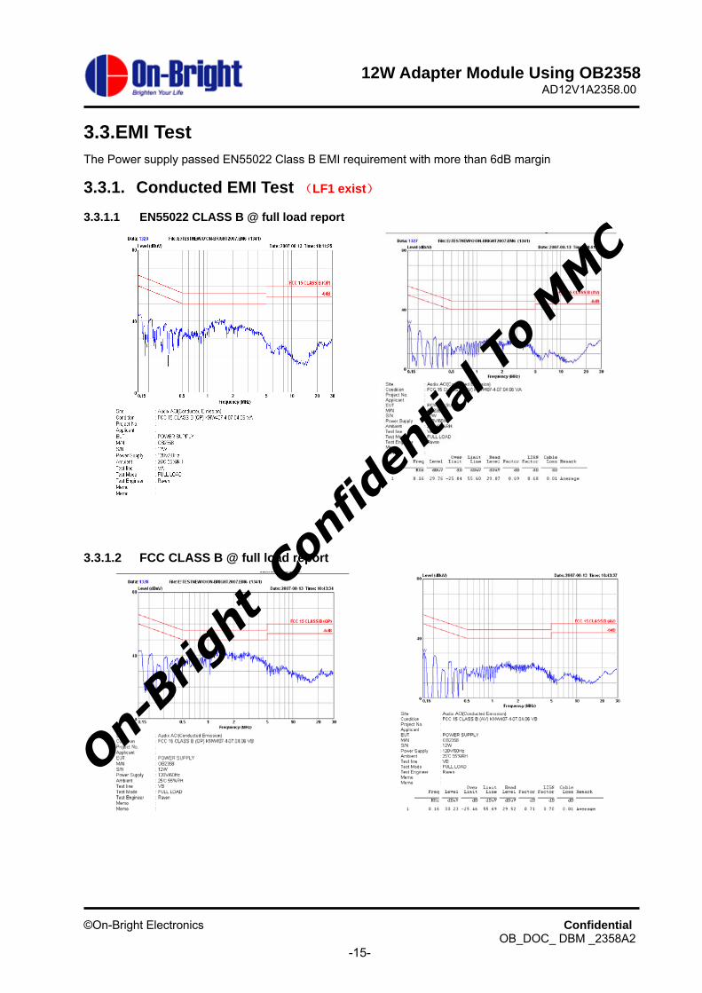
3.3.EMI Test The Power supply passed EN55022 Class B EMI requirement with more than 6dB margin
3.3.1. Conducted EMI Test (LF1 exist)
3.3.1.1 EN55022 CLASS B @ full load report
3.3.1.2 FCC CLASS B @ full load report
On-Brig
ht C
onfid
entia
l To
MMC

©On-Bright Electronics Confidential
OB_DOC_ DBM _2358A2 -16-
12W Adapter Module Using OB2358 AD12V1A2358.00
3.3.2. Radiation EMI Test (LF1 exist) 3.3.2.1.EN55022 CLASS B @ full load report
3.3.2.2.FCC CLASS B @ full load report
On-Brig
ht C
onfid
entia
l To
MMC

©On-Bright Electronics Confidential
OB_DOC_ DBM _2358A2 -17-
12W Adapter Module Using OB2358 AD12V1A2358.00
3.3.3. Conducted EMI Test (NO LF1)
3.3.3.1 EN55022 CLASS B @ full load report
3.3.3.2 FCC CLASS B @ full load report
On-Brig
ht C
onfid
entia
l To
MMC

©On-Bright Electronics Confidential
OB_DOC_ DBM _2358A2 -18-
12W Adapter Module Using OB2358 AD12V1A2358.00
3.3.4. Radiation EMI Test (NO LF1) 3.3.4.1 EN55022 CLASS B @ full load report
3.3.4.2 FCC CLASS B @ full load report
On-Brig
ht C
onfid
entia
l To
MMC

©On-Bright Electronics Confidential
OB_DOC_ DBM _2358A2 -19-
12W Adapter Module Using OB2358 AD12V1A2358.00
4. Protection
4.1. Over voltage protection Table. 8 OVP @ no load
Input OVP Protection 115Vac/60Hz OK 230Vac/50Hz OK
4.2. Short circuit protection The system is protected during output short circuit condition and recovered when short circuit condition is removed.
Fig. 18 Output short, Vds waveform@264 Vac/50Hz, full load
4.3. Over Load Protection Table. 9 OLP @ Full load
Input OLP Protection 115Vac/60Hz OK 230Vac/50Hz OK
On-Brig
ht C
onfid
entia
l To
MMC

©On-Bright Electronics Confidential
OB_DOC_ DBM _2358A2 -20-
12W Adapter Module Using OB2358 AD12V1A2358.00
5. Thermal Testing
Vin Po Environment IC Transformer
(winding ) 85Vac 12W(load1A) 40 96.1 85.2
Case: Φ72.5mmX27.3mmX42mm
On-Brig
ht C
onfid
entia
l To
MMC

©On-Bright Electronics Confidential
OB_DOC_ DBM _2358A2 -21-
12W Adapter Module Using OB2358 AD12V1A2358.00
6. Other Important Waveform 6.1. Vdd, Sense& FB&Vds wave form @ no load /full load
Fig. 19 Vdd, Sense&FB&Vds waveform@90Vac/60Hz, ,full load Fig. 20 Vdd,Sense &FB&Vds waveform @264Vac/50Hz, full load
6.2. MOSFET Vds waveform @ start/normal/output short
Fig. 21 Start, Vds waveform@90 Vac/60Hz, full load Fig. 22 Start, Vds waveform@264 Vac/50Hz, full load
Fig. 23 Normal, Vds waveform@264 Vac/50Hz, full load Fig. 24 Output short, Vds waveform@264 Vac/50Hz,
On-Brig
ht C
onfid
entia
l To
MMC

©On-Bright Electronics Confidential
OB_DOC_ DBM _2358A2 -22-
12W Adapter Module Using OB2358 AD12V1A2358.00
Table. 10 Vds_max @ Full load / Output short
Input Vds_max(V)
264Vac/50Hz @No load 563
264Vac/50Hz @ Full load 538
264Vac/50Hz @ Output short 513
Disclaimer On-Bright Electronics reserves the right to make corrections, modifications, enhancements, improvements, and other changes to its documents, products and services at any time and to discontinue any product or service without notice. Customers should obtain the latest relevant information before placing orders and should verify that such information is current and complete. This document is under copy right protection. Non of any part of document could be reproduced, modified without prior written approval from On-Bright Electronics.
On-Brig
ht C
onfid
entia
l To
MMC