Embed Size (px)
Citation preview

IJECT Vol. 6, IssuE 4, oCT - DEC 2015 ISSN : 2230-7109 (Online) | ISSN : 2230-9543 (Print)
w w w . i j e c t . o r g 52 InternatIonal Journal of electronIcs & communIcatIon technology
Low Power Design Techniques for Reduction of Leakage Power in CMOS VLSI Circuits using Modified Sleepy Keeper
1Achala Yadav, 2Ritish Kumar1,2Dept, of VLSI Engineering, Shobhit University, Meerut, Uttar Pradesh
AbstractScaling of transistor features sizes has improves performance, increase transistor density and reduces the power consumption. A chip’s maximum power consumption depends on its technology as well as its implementation. As technology scales down and CMOS circuits are powered by lower supply voltages, standby leakage current becomes significant. As the threshold voltage is reduced due to scaling, it leads to increase in sub threshold leakage current and hence increase in static power dissipation. This paper presents performance analysis of inverter using conventional CMOS, stack and dual threshold transistor stacking, sleepy stack, sleepy keeper technique etc. The performance analyses of inverter were analyzed in 90nm technology using Virtuoso software (cadence). In order to reduce the static power dissipation, one has to sacrifice circuit performance and area. This paper presents the comparative study of all the approaches. In the proposed circuit the utilization of the sleepy keeper approach with stacking of transistor is incorporated for further reduction of the leakage power.
KeywordsCMOS Inverter, Cadence, Static Power, Sleepy Keeper, Threshold Voltage, Transistor Stacking.
I. IntroductionThe power is emerging as the most critical and vital issues in system on chip design today and management of power in every category of design is becoming an increasingly urgent problem. In early 1970’s, providing high speed operation with minimum area were main aim of design. Many design tools are concentrated to achieve these goals.
Fig. 1: Design Parameters
However, introducing the third parameter of power dissipation made the designers to change the flow as shown fig. 1.In CMOS VLSI circuits, power dissipation is basically due to the three important and major components: dynamic, static and short circuit. The switching activity is given by [8].
(1)Where Fi is input signal frequency, Cpd dynamic power dissipation capacitance, V is the supply voltage. Due to the growing demand of battery operated devices, the power consumption has become a vital and major problem of integrated circuit designer. Scaling has result exponential increase in the leakage current [8]. The subthreshold leakage current Ileakage can be given as:
(2)
Where,
Cox is the gate oxide capacitance, (W/L) is the width to length ratio of the MOS device, μ0 is the zero bias mobility, Vgs is the gate to source voltage, VT is the thermal voltage and η is the sub threshold coefficient. Several techniques have been proposed to reduce leakage power. One important thing in CMOS VLSI circuit design is to lower the power dissipation while maintaining the high performance of the circuit to maintain the performance of the circuit. To maintain the circuit performance it is needed to scale the threshold voltage. For low threshold age transistors which are fast have high threshold leakage current are used to implement the logic. High threshold which are slow and have low sub threshold leakage current. The propagation delay is given by [8].
(3)
Where C is the total load capacitance Vdd is the supply voltage, Vt is the threshold voltage and α model short channel effect.ITRS reported that leakage power consumption may come to dominate total chip power consumption as technology feature size shrinks [6, 8]. It can observe be that static consumption tends to increase over the year as dynamic power consumption [11]. The increasing prominence of portable systems and the need to limit power consumption in very high density ULSI chips have lead to rapid and innovative development in low power design. Due to power sensitive portable devices, low power is very important requirement of all high performance application where power is one of the important design constraints.
Fig. 2: Power Consumption Prediction by the ITRS
In today’s era of VLSI, power consumption control and management has become a key challenge and critical issue in electronics industry. The advancement in VLSI technology allows integrating a complete system on chip (SoC) providing facility to develop a portable system. Power dissipation is a critical parameter in battery operated portable device. The limited battery Lifetime typically imposed very strict demands on the overall

IJECT Vol. 6, IssuE 4, oCT - DEC 2015
w w w . i j e c t . o r g InternatIonal Journal of electronIcs & communIcatIon technology 53
ISSN : 2230-7109 (Online) | ISSN : 2230-9543 (Print)
power consumption of the portable systems. Power consumption is one of the important factors of VLSI circuit design for CMOS is the primary technology. The power consumption has become a fundamental problem in VLSI circuit design. Therefore, reducing the power consumption of integrated circuits through design improvement is a major challenge in portable system design. To solve the power consumption problem, many different techniques from circuit level to device level and above have been proposed by researchers. However, there is no straight forward ways to meetthe tradeoff between power, delay and area. The designers are required to choose appropriate techniques that satisfy the application and product needs [3]. Reducing power dissipation varies from application to application. The key objective in reducing power consumption is to reduce the overall cost the product. One of the most challenging problem is to find out new and effective circuit design technique to reduce the overall power dissipation without compromising the performance of the device. Scaling advanced CMOS technology improves high performance and high transistor density. The power dissipation of a chip depends not only on its technology but also on its implementation i.e on size, circuit style, operating frequency and so on. Because of this technology trends transistor leakage power has increased exponentially supply voltage scaling increases sub-threshold leakage current, increases leakage power and pose numerous leakage in the VLSI design. Therefore static power has become a significant portion of the total power consumption. There are several VLSI techniques to reduce leakage power. Different techniques provide an efficient way to reduce leakage power, but disadvantages of each technique limit the application of each technique. In this paper an efficient sub-threshold leakage current reduction and optimization methods are presented and result are given for 90nm generic process design kit technology using virtuoso schematic editor.
II. Subthreshold Leakage Power Reduction TechniquesFig. 3, shows that sub threshold leakage current (power) is becoming the primary source of power dissipation is CMOS below 90nm. At smaller geometries, management of leakage current can greatly impact design and implementation choices [9]. Till now, primary concerned were improving the performance of design and reducing silicon area to lower the cost. Now power is replacing performance as the key metric for VLSI design.
Fig. 3: Process Technology vs. Leakage and Dynamic Power
A. Conventional CMOS TechniqueFig. 4, shows the block diagram of digital circuit using conventional CMOS techniques. In this technique, a fully complementary CMOS circuit has an nMOS pull down network to connect the output to ’0’ (GND) and pMOS pull up network to connect the output to ’1’ (VDD).
Fig. 4: Base Case (Conventional CMOS) Circuit Structure
B. Stack TechniqueThis technique is based on the fact that natural stacking of MOS-FET helps in achieving leakage current. The leakage through two series OFF transistor is much lower than that of single transistor because of stack effect [4]. An effective way to reduce leakage power in active mode is stacking of transistor [1].
Fig. 5: Stack Technique Circuit Structure
Fig. 6: Circuit Schematic of Forced Stack Technique

IJECT Vol. 6, IssuE 4, oCT - DEC 2015 ISSN : 2230-7109 (Online) | ISSN : 2230-9543 (Print)
w w w . i j e c t . o r g 54 InternatIonal Journal of electronIcs & communIcatIon technology
The subthreshold leakage is exponentially related to the threshold voltage of the device and threshold voltage changes due to body effect. The source of the nMOS device N1 is connected to ground. Transistor N2 source is connected to drain of N1. The source of N2 is not grounded and it can acquire voltages close to Vdd while its substrate is connected to ground. Therefore the condition Vsb=0 will not hold in bias cases for transistor N2. The device N1 will experience higher Vth due to the difference in the voltage between the source and body. The voltage between drain and source also decreased since the intermediate node has a voltage above the ground resulting reduction in DIBL affect and hence effective saving of leakage power. For turned off the single transistor, leakage current Isub0 can be expressed as follows [3, 8]:
(4)
(5)
(6)
n=sub-threshold coefficient V=thermal voltage Vgs0; Vth0; Vbs0 and Vds0 are the gate-to-source voltage, the zero-bias threshold voltage, the base -to-source voltage and the drain-to-source voltage respectively. γ is the bodybias effect coefficient, and η is the Drain Induced Barrier Lowering (DIBL) coefficient. μ is zero-bias mobility, Cox is the gate-oxide capacitance, W is the width of the transistor, and Leff is the effective channel length. Two transistor are turned off together (M1=M2). So,
(7)
(8)
Where Vx is the voltage at the node between M1 and M2. Now consider X is the factor of Isub0 and Isub1 (== Isub2)
If Isub1 = Isub2 the above form of equation can be written as:
The threshold voltage can be controlled by body bias effect.
(12)
Changing the substrate voltage causes the threshold voltage to change. So the different kind of effect is arises for changing the substrate voltage like Zero-Body Bias, Reverse-Body Bias and Forward-Body Bias. This Phenomenon is frequently used for con trolling the threshold voltage. Constant dependent on the transistor parameter and the technology feature size. By controlling body biasing effect with changing the constant term can easily control the leakage power [3,7].
Fig. 7: Circuit Schematic of Forced Stack Technique
Fig. 7, shows the leakage current trends of each stacked transistor as a function of number of stacked transistor.
C. Sleep Transistor TechniqueThis technique uses the sleep transistor between both VDD and the pull up network and between GND and pull down network [3]. The sleep transistor turn off the circuit by cutting off the power rails in idle mode thus can reduce leakage power effectively.In this technique we have floating values and thus will lose state during sleep mode. The Wakeup time and energy of the sleep technique have significant impact [3]. The technique in which high Vth sleep transistor are used called Multithreshold voltage CMOS (MTCMOS) proposed by Motoh et al. [3].
Fig. 8: Sleep Transistor Technique Structure
D. Dual Threshold Transistor Stacking TechniqueThis new technique called dual threshold transistor stacking hybrid version of stack and MTCMOS. It takes the advantage of both techniques i.e sleep transistors are redesigned with stack effect. The size of sleep transistor is reduced. The sleep transistors are designed as a high threshold voltage [1]. Fig. 9, shows the circuit schematic of dual threshold transistor stacking technique.

IJECT Vol. 6, IssuE 4, oCT - DEC 2015
w w w . i j e c t . o r g InternatIonal Journal of electronIcs & communIcatIon technology 55
ISSN : 2230-7109 (Online) | ISSN : 2230-9543 (Print)
Fig. 9: Dual Threshold Transistor Stacking Technique Structure
E. Sleepy Stack Transistor Technique
Fig. 10: Sleepy Stack Technique Structure
The forced stack and the sleep transistor techniques are combined to get the sleepy stack structure. The function of sleep transistors in sleepy stack is same as of the sleep transistor in sleep transistor technique. During sleep mode, sleep transistors are turned off and stacked transistors suppress leakage current [3][9]. The drawback of this technique is increase in area.
F. Sleepy Keeper Approach
Fig. 11: Sleepy Keeper Structure
Sleepy keeper uses leakage feedback technique [9]. PMOS transistors are not efficient at passing GND and NMOS transistors are not efficient at passing VDD. In this technique, a PMOS transistor is placed in parallel to the sleep transistor (s) and a NMOS transistor is placed parallel to the sleep transistor (s’). The sleep transistors are turned off during sleep mode and transistor in parallel to sleep transistor keep the contact with the appropriate power rail [9].
G. Variable Body Biasing Technique
Fig. 12: Structure of Variable Body Biasing Technique

IJECT Vol. 6, IssuE 4, oCT - DEC 2015 ISSN : 2230-7109 (Online) | ISSN : 2230-9543 (Print)
w w w . i j e c t . o r g 56 InternatIonal Journal of electronIcs & communIcatIon technology
in sleep mode to reduce the leakage current. For this in sleepy keeper technique a PMOS and NMOS is added. During sleep mode PMOS is OFF so the body to source voltage of the pull up PMOS is higher than in the active mode. From equation (7), the leakage current decreases as Vsb1 increases. The body effect, vth also increases due to which performance gets degrade [9]. As shown in Figure 12, this technique uses two parallel sleep transistors in pull up network and two parallel sleep transistors in pull down network. For body biasing effect, the source of one of the PMOS sleep transistor is connected to the body of the other PMOS sleep transistor. On the other hand the source of the NMOS sleep transistor is connected to the body of other NMOS sleep transistor. The variable body biasing techniques uses PMOS transistor in GND and NMOS transistor in VDD, both are in paralleled to the sleep transistor for maintaining exact logic state during the sleep mode [9].
III. Simulation ResultsSimulations have been performed using virtuoso (cadence) in 90 nanometer (nm) gpdk CMOS technology with supply
Fig. 13: Inverter With Conventional Technique
Fig. 14: Input and Output Waveform of Inverter With Conventional Technique
voltage 1.2V to estimate power consumption. The static power consumption, dynamic power consumption and propagation delay measured for different design techniques. Fig. 13, to Fig. 24, shows the resulting schematic diagram, input-output waveforms of each technique. Fig. 23, shows the static power consumption, Fig. 25, shows the dynamic power consumption and Fig. 26, shows the propagation delay comparison chart.
Fig. 15: Inverter With Stack Technique
Fig. 16: Input and Output Waveform of Inverter With Stack Technique

IJECT Vol. 6, IssuE 4, oCT - DEC 2015
w w w . i j e c t . o r g InternatIonal Journal of electronIcs & communIcatIon technology 57
ISSN : 2230-7109 (Online) | ISSN : 2230-9543 (Print)
Fig. 17: Inverter with Sleep Transistor Technique
Fig. 18: Input and Output waveform of Inverter with Sleep Transistor Technique
Fig. 19: Inverter with Dual Threshold Stack Transistor Technique
Fig. 20. Input and Output Waveform of Inverter With Dual Threshold Stack Transistor Technique
Fig. 21: Inverter With Sleepy Keeper Technique
Fig. 22: Input and Output Waveform of Inverter With Sleepy Keeper Technique

IJECT Vol. 6, IssuE 4, oCT - DEC 2015 ISSN : 2230-7109 (Online) | ISSN : 2230-9543 (Print)
w w w . i j e c t . o r g 58 InternatIonal Journal of electronIcs & communIcatIon technology
Fig. 23: Inverter With Sleepy Stack Technique
Fig. 24: Input and Output Waveform of Inverter With Sleepy Stack Technique
Fig. 25: Static Power Comparison
Fig. 26: Dynamic Power Comparison
Fig. 27: Propagation Delay Comparison
Fig. 28: Chain of Inverter With Base Case Approach

IJECT Vol. 6, IssuE 4, oCT - DEC 2015
w w w . i j e c t . o r g InternatIonal Journal of electronIcs & communIcatIon technology 59
ISSN : 2230-7109 (Online) | ISSN : 2230-9543 (Print)
Fig. 29: Input and Output Waveform of Chain of Inverter With Base Case Approach
Fig. 30: Chain of Inverter with Sleep Transistor Technique
IV. Proposed WorkIn this section, a new Modified Sleepy Keeper with Stacking of the Transistor with High Vth Low Vth Transistor has been proposed. The proposed circuit is compared with well-known previous approaches, i.e., Basic NAND Gate, Forced stacking, Sleep transistor with Low Vth, Sleep transistor with High Vth Sleepy Keeper. Firstly the proposed NAND gate circuit operation is explained. In sleep mode, the sleep transistors are off, i.e. transistor M1, M2 and Y1,Y2 are off. We do so by making S=0 and hence S’=1. Now see that the working of the basic NAND gate the output of the NAND gate is one either input is Zero with different combination of the input vector. In the proposed Circuit the utilization of the sleepy keeper Approach with Stacking of the transistor is incorporated for further reduction of the Leakage power in the circuit.
Fig. 31: Proposed Technique With High Vth Transistors
Fig. 32: Output Waveform of the Proposed Circuit
A. Results and DiscussionSimulation is performed of various leakage reduction technique like basic 2 3 input NAND gate, sleep approach, sleepy keeper and sleepy stack and proposed approach using BISM4 Cadence virtuoso with 1V supply at 65nm channel length for reduction of average power delay and calculation of leakage current. The circuits are simulated with high threshold and low threshold NMOS and PMOS transistors.
IJECT Vol. 6, IssuE 4, oCT - DEC 2015 ISSN : 2230-7109 (Online) | ISSN : 2230-9543 (Print)
w w w . i j e c t . o r g 60 InternatIonal Journal of electronIcs & communIcatIon technology
Fig. 33: Layout Diagram of Proposed Circuit
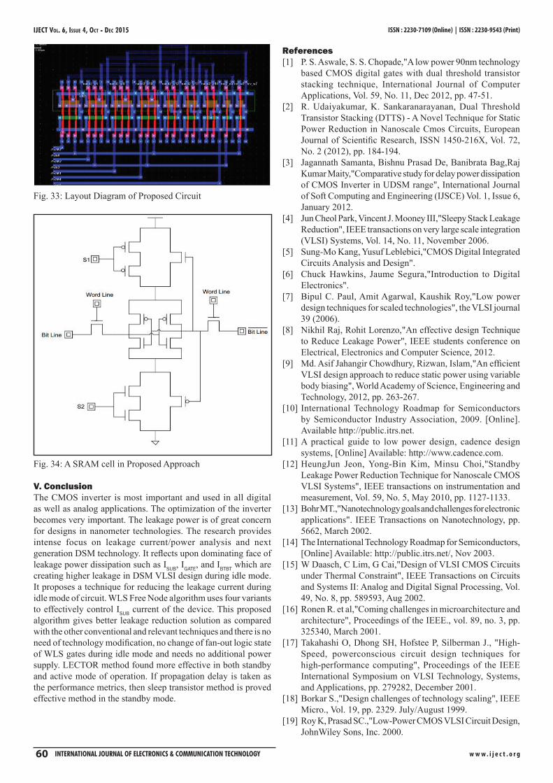
Fig. 34: A SRAM cell in Proposed Approach
V. ConclusionThe CMOS inverter is most important and used in all digital as well as analog applications. The optimization of the inverter becomes very important. The leakage power is of great concern for designs in nanometer technologies. The research provides intense focus on leakage current/power analysis and next generation DSM technology. It reflects upon dominating face of leakage power dissipation such as ISUB, IGATE, and IBTBT which are creating higher leakage in DSM VLSI design during idle mode. It proposes a technique for reducing the leakage current during idle mode of circuit. WLS Free Node algorithm uses four variants to effectively control ISUB current of the device. This proposed algorithm gives better leakage reduction solution as compared with the other conventional and relevant techniques and there is no need of technology modification, no change of fan-out logic state of WLS gates during idle mode and needs no additional power supply. LECTOR method found more effective in both standby and active mode of operation. If propagation delay is taken as the performance metrics, then sleep transistor method is proved effective method in the standby mode.
References[1] P. S. Aswale, S. S. Chopade,"A low power 90nm technology
based CMOS digital gates with dual threshold transistor stacking technique, International Journal of Computer Applications, Vol. 59, No. 11, Dec 2012, pp. 47-51.
[2] R. Udaiyakumar, K. Sankaranarayanan, Dual Threshold Transistor Stacking (DTTS) - A Novel Technique for Static Power Reduction in Nanoscale Cmos Circuits, European Journal of Scientific Research, ISSN 1450-216X, Vol. 72, No. 2 (2012), pp. 184-194.
[3] Jagannath Samanta, Bishnu Prasad De, Banibrata Bag,Raj Kumar Maity,"Comparative study for delay power dissipation of CMOS Inverter in UDSM range", International Journal of Soft Computing and Engineering (IJSCE) Vol. 1, Issue 6, January 2012.
[4] Jun Cheol Park, Vincent J. Mooney III,"Sleepy Stack Leakage Reduction", IEEE transactions on very large scale integration (VLSI) Systems, Vol. 14, No. 11, November 2006.
[5] Sung-Mo Kang, Yusuf Leblebici,"CMOS Digital Integrated Circuits Analysis and Design".
[6] Chuck Hawkins, Jaume Segura,"Introduction to Digital Electronics".
[7] Bipul C. Paul, Amit Agarwal, Kaushik Roy,"Low power design techniques for scaled technologies", the VLSI journal 39 (2006).
[8] Nikhil Raj, Rohit Lorenzo,"An effective design Technique to Reduce Leakage Power", IEEE students conference on Electrical, Electronics and Computer Science, 2012.
[9] Md. Asif Jahangir Chowdhury, Rizwan, Islam,"An efficient VLSI design approach to reduce static power using variable body biasing", World Academy of Science, Engineering and Technology, 2012, pp. 263-267.
[10] International Technology Roadmap for Semiconductors by Semiconductor Industry Association, 2009. [Online]. Available http://public.itrs.net.
[11] A practical guide to low power design, cadence design systems, [Online] Available: http://www.cadence.com.
[12] HeungJun Jeon, Yong-Bin Kim, Minsu Choi,"Standby Leakage Power Reduction Technique for Nanoscale CMOS VLSI Systems", IEEE transactions on instrumentation and measurement, Vol. 59, No. 5, May 2010, pp. 1127-1133.
[13] Bohr MT.,"Nanotechnology goals and challenges for electronic applications". IEEE Transactions on Nanotechnology, pp. 5662, March 2002.
[14] The International Technology Roadmap for Semiconductors, [Online] Available: http://public.itrs.net/, Nov 2003.
[15] W Daasch, C Lim, G Cai,"Design of VLSI CMOS Circuits under Thermal Constraint", IEEE Transactions on Circuits and Systems II: Analog and Digital Signal Processing, Vol. 49, No. 8, pp. 589593, Aug 2002.
[16] Ronen R. et al,"Coming challenges in microarchitecture and architecture", Proceedings of the IEEE., vol. 89, no. 3, pp. 325340, March 2001.
[17] Takahashi O, Dhong SH, Hofstee P, Silberman J., "High-Speed, powerconscious circuit design techniques for high-performance computing", Proceedings of the IEEE International Symposium on VLSI Technology, Systems, and Applications, pp. 279282, December 2001.
[18] Borkar S.,"Design challenges of technology scaling", IEEE Micro., Vol. 19, pp. 2329. July/August 1999.
[19] Roy K, Prasad SC.,"Low-Power CMOS VLSI Circuit Design, JohnWiley Sons, Inc. 2000.

IJECT Vol. 6, IssuE 4, oCT - DEC 2015
w w w . i j e c t . o r g InternatIonal Journal of electronIcs & communIcatIon technology 61
ISSN : 2230-7109 (Online) | ISSN : 2230-9543 (Print)
[20] Flynn MJ, Hung P, Rudd KW., Deep submicron microprocessor design issues", IEEE Microelectronics Journal., Vol. 19, pp. 1122, July/August 1999
[21] Borkar S.,"Obeying Moores law beyond 0.18 micron", Proceedings of the IEEE International ASIC/SOC Conference, pp. 2631, September 2000.