Embed Size (px)
Citation preview
doc.: IEEE 802.15-12-0621November 2012
Project: IEEE P802.15 Working Group for Wireless Personal Area Networks (WPANs)Project: IEEE P802.15 Working Group for Wireless Personal Area Networks (WPANs)Project: IEEE P802.15 Working Group for Wireless Personal Area Networks (WPANs)Project: IEEE P802.15 Working Group for Wireless Personal Area Networks (WPANs)
Submission Title: The Next Frontier for Circuit Designers: CMOS THz Systems Date Submitted: 13 November 2012Source: Ehsan Afshari Company: Cornell UniversityAddress 424 Phillips Hall, Cornell university, Ithaca, NY 14850Voice:[607-255-0603], FAX: [6072544208], E-Mail: [email protected] Re: /Re: n/a
Abstract: There has been a growing interest in mm-wave and Terahertz frequencies for communication, imaging and sensing applications In this talk we will look into recent advances in CMOS implementationimaging, and sensing applications. In this talk, we will look into recent advances in CMOS implementation of various building blocks. First, we show how to implement mW-level signals up to 500GHz. Then we show different amplifiers as well as two transmitters at 260GHz and 350GHz.
P I f ti t IEEE 802 15 IG THPurpose: Information to IEEE 802.15 IG THzNotice: This document has been prepared to assist the IEEE P802.15. It is offered as a basis for discussion and is not binding on the contributing individual(s) or organization(s). The material in this document is subject to change in form and content after further study The contributor(s) reserve(s) the rightdocument is subject to change in form and content after further study. The contributor(s) reserve(s) the right to add, amend or withdraw material contained herein.Release: The contributor acknowledges and accepts that this contribution becomes the property of IEEE and may be made publicly available by P802.15.
Submission Ehsan Afshari (Cornell University)Slide 1

Ehsan Afshari Cornell University
(http://unic.ece.cornell.edu)
November 2012
The Next Frontier for Circuit Designers: CMOS THz Systems

Acknowledgement
• The people who actually make it happen!

Our Research
High FrequencyTHz OscillatorTHz AmplifierTHz MultiplierTHz Imaging
Noise SqueezingCoupled Systems
Low NoiseOscillator
VCOAmplifier
Noise SqueezingADC
Low powerHigh Speed
Biological Systems
New Science New Techniques

Other Projects
• Low phase noise oscillators: – Dual mode,
– Quadrature.
• Wideband low phase noise VCO: – 2.4GHz – 5.6GHz that satisfies ALL cellular specifications
• Low power, high speed ADC – 8GS/sec, 4b with 32mW
– 1.2GS/sec, 4b with 2mW
• Narrow pulse generation on CMOS – 1.6ps pulse on standard 65nm CMOS
• A 260GHz Amplifier – 9.2dB gain
– -4dBm Psat
Cc
Cc
LM
CLC
Gmc
Gmc
-Gm
Gmc
Gmc
-Gm

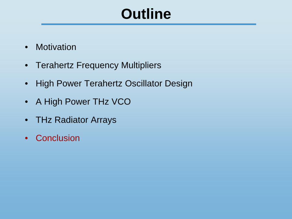
Outline
• Motivation
• Terahertz Frequency Multipliers
• High Power Terahertz Oscillator Design
• A High Power THz VCO
• THz Radiator Arrays
• Conclusion

• Imaging (e.g., detection of concealed weapon, cancer diagnosis, and semiconductor wafer inspection )
• Compact range radars
• High data rate communication (e.g.,100 Gbps)
High power is needed for these applications
Application of THz Systems

• Skin cancer detection:
– Large tumors can extend 15mm beyond the visible border
– Significant number occur on face
– Existing techniques can have high false negative rates and is time and personnel intensive
– At 700GHz, we can have 40µm depth resolution and 1mm penetration
• Tooth decay:
– Small cavities are hard to detect
– Earlier detection equates to better outcomes
– X-ray has limited resolution
Application of THz Systems

• Corneal hydration sensing: – Diseases and procedures:
• Corneal Graft surgery • Fuch’s Dystrophy • Keratoconus • Glaucoma • LASIK
– Current methods based on ultrasonic or optical thickness measurements
– Thickness measurement very accurate (~ 9 um) – Mapping from thickness to hydration very inaccurate
(+/- 5% by volume) – Physiologic variation confounds measurement – Listed diseases and procedures need hydration
sensitivity in the range of 0.8% - 3% depending on application
– THz imaging results in better than 0.2% sensitivity
Application of THz Systems
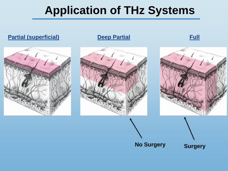
Application of THz Systems
Partial (superficial) Deep Partial Full
No Surgery Surgery
Application of THz Systems
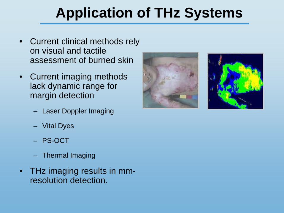
• Current clinical methods rely on visual and tactile assessment of burned skin
• Current imaging methods lack dynamic range for margin detection
– Laser Doppler Imaging
– Vital Dyes
– PS-OCT
– Thermal Imaging
• THz imaging results in mm-resolution detection.

Fundamental Challenges: • Transistors offer no power gain above fmax • Limited power efficiency of devices • Limited break down voltage • Quality factor of passives is low
High power signal generation is the main challenge in realizing CMOS THz systems.
Challenge
Electronic Source progress Optical Source
progress
Solid-State THz Sources (CW)
Electronic Source progress Optical Source
progress

Terahertz Electronic Sources
• Travelling electron beams – Example: BWO – Up to 1 mW around 1 THz – Very bulky and expensive
• Josephson arrays – Quantum tunneling in superconductors – Cryogenic temperatures – < 1µW power levels
• Solid-state devices – Limited by electron scattering – InP devices: 100 µW to 1 mW around 400 GHz

Solid-State Devices for Terahertz
• Diodes (Gunn, IMPATT, Tunneling, etc.) • Compound semiconductor transistors (InP HBT, GaN
HEMT, etc.) Large breakdown voltages (i.e. GaN > 20 V) High cut-off frequency (fmax ~ 1 THz) x Expensive material x Not suitable for large scale integration
• CMOS transistors Cheap and versatile technology x Low supply voltage (~ 1.2 V) x Low cut-off frequency (fmax< 0.25 THz)
A CMOS Terahertz solution is highly desirable but challenging

Signal Generation Above Cut-off
• A nonlinear process generates harmonics of the fundamental frequency above fmax .
• Device nonlinearity can be exploited – Diodes: IMPATT, Gun, Tunneling, Schottky – Transistors: HBT, HEMT, CMOS
• Two approaches: Multiplier : a high power source is normally
provided off-chip. Harmonic oscillator : The oscillator is
implemented on chip • On-chip implementation is the ultimate
solution
fo N x fo
High PowerOff-chip Nonlinearity
DC N x fosc
Active device

Outline
• Motivation
• Terahertz Frequency Multipliers
• High Power Terahertz Oscillator Design
• A High Power THz VCO
• THz Radiator Arrays
• Conclusion

• Effective harmonic generation and combining
Zoωo
Cd
Vout
Lg
A
RLBias-T
Ld
Cg
Cm
Lm
Basic Idea

• Effective harmonic generation and combining
Zo
Cd
Vout
Lg
A
RLBias-T
Ld
Cg
Cm
Lm-R @ ωo
Matched @ nωo
ωo• Efficient loss cancellation
Basic Idea

Theory
2Zo
ωo= 2πfo
Lg
ALg/2
φ phase shift
V1=cos(ωot)+cos(ωot - k- φ - k ) V2=cos(ωot- k)+cos(ωot - k- φ)
V2V1
I2=a1V2+a2V22=…+a2cos(2ωot - 2k- φ)+...I1=a1V1+a2V2
2=…+a2cos(2ωot - 2k- φ)+...
ggCLk °= ω
reflected
incident
reflected
incident
• The second harmonics add in phase at the output • The basic principle is independent of frequency
W
fo
Lin
Lg
A
Cg

Zin
Ld
-4
-2
0
2
4
120 125 130 135 140 145 150
Ld=68 pH
Ld=60 pH
Ld=53 pH
Ld=46 pHLd=40 pH
Input Frequency (GHz)
Rea
l(Zin
) (Ω
)
• There is a trade-off between better output matching and higher input voltage swing.
Negative Input Impedance
1)gR
CC(CωL
m
gddsgd
2d <++
Real(Zin) < 0

Implementation
• The power and frequency test setups
250 µm
200
µm
Vin
Vout
DUT
Cascade i325-GSG Probe
WR-3.0 waveguide
Harmonic mixer
OMLWR-3.0
Diplexer OMLIF
LO
Signal Generator
4 - 7 GHz
(Agilent E8257D)
(Agilent 8564E)
Spectrum Analyzer
Bias-tee
Power Supply
VddVGS
GGB 140-GSG Probe
WR-8.0 waveguide
VDIWR-8.0X3
Frequency Tripler
Signal Generator
36 - 47 GHz
(Agilent E8257D)
Amplifier(Centellax A4MVM3)
DUT
Cascade i325-GSG Probe
WR-3.0 waveguide
Bias-tee
VGS
GGB 140-GSG Probe
WR-8.0 waveguide
VDIWR-8.0X3
Frequency Tripler
Signal Generator
36 - 47 GHz
(Agilent E8257D)
Amplifier(Centellax A4MVM3) Power Supply
Vdd
WR-3.0 to WR-10 tapered waveguide
Power-meter(Erickson PM4)
Sensor head
µW

Results
220 230 240 250 260 270 280-30
-25
-20
-15
-10
-5
5
10
15
20
25
30
P out
@ 2
f 0 (d
Bm
)
Frequency (GHz)
Con
vers
ion
loss
(dB)
• In this case the input power is kept at 3dBm

Results
-8 -6 -4 -2 0 2 4 6-30
-25
-20
-15
-10
-5
10
12
14
16
18
20
P out
(dBm
) @ 24
4 G
Hz
Pin (dBm) @ 122 GHz
Conv
ersi
on lo
ss (d
B)
• The output power is not saturated • A maximum of -6.6dBm is achieved at 244GHz

• Main structure: a compact partially-coupled ring
• Simultaneous matching at fundamental (input) and 2nd harmonic (output)
– Pads are part of the input/output matching
– Rp1 and Rp2: leakage paths for accumulative charge to avoid oxide breakdown
A 480 GHz Doubler

Experimental Results
– 65nm Bulk LP CMOS

Outline
• Motivation
• Terahertz Frequency Multipliers
• High Power Terahertz Oscillator Design
• A High Power THz VCO
• THz Radiator Arrays
• Conclusion

Fundamental Limit?
• Most of the fundamental oscillators have the oscillation
frequency in the order of the half of the fmax of the
transistors. Why not higher?
• What is the maximum oscillation frequency of a circuit
topology, considering the quality factor of the passive
components?
• For a fixed frequency, what is the topology that results in
maximum output power?

Fundamental Limit • Example: IBM 130 nm CMOS process:
– fmax: simulated: 174 GHz
– fmax: measured: ~135 GHz
• Regular Cross-Coupled oscillator: – Maximum achievable frequency (simulation): 120 GHz
– This is with IDEAL inductors! VDD

Activity Condition
• Normalized real power flowing out of the device:
I2
V2
+
−
I1
V1
+
−
[ ]
=
2
1
2
1
VV
YII
))(cos()( 2112211222111
21
ϕ++∠+−+−==⇒ ∗∗− YYYYAGGAVV
PG Rm
)()(
2222
1111
YrealGYrealG
==
)(&1
2
1
2
VV
VVA ∠== ϕ
• Gm is the maximum conductance that can be placed across the transistor and maintain the oscillation.

Maximum Activity
• Optimum gain and phase conditions for maximum generated power (maximum oscillation frequency)
22
11
GGAA opt ==)()12( *
2 11 2 YYko p t +∠−+== πϕϕ
φ opt
(deg
ree)
Aopt
0.1
0.2
0.3
0.4
0.5
0.6
0.7
0.8
0.9
1
1.1
1.2
100
110
120
130
140
150
160
170
180
Frequency (GHz)
0 25 50 75 100 125 150 175 200

Higher Frequency: Harmonics
• In order to achieve higher frequencies, we need to generate
strong harmonics
• This means we should maximize the swing at the fundamental
frequency
• It might be better to back off from the maximum possible
oscillation frequency to boost the harmonic generation
• We need to maximize “Gm”

Optimum Conditions
• Optimum phase and voltage conditions in a 65nm process • Target frequency is 450 GHz
50 100 150 200 250 300
145
150
155
160
165
170
175
Frequency (GHz)
1.0
0.8
0.6
0.4
0.2
Opt
imum
ϕ (d
egre
e)
Opt
imum
Α
+
−
+
−V2V1

Triple Push Oscillator
Ld
W
Vout
RL=50 Ω
Lg
Bia
s-te
e
ZD
ZG
+
-V1
+
-
V2
optAVVA ≅=
1
2
optVV ϕϕ ≅∠= )(
1
2
• The gate inductor helps
with both amplitude
and phase conditions:
– It resonates with Cgs to
boost the gate-source
voltage, resulting in
lower A across the
device
– It also delays the voltage
to increase the phase
shift from 120.

Implementation
200 µm
110
µm
VoutDUT
Cascade i500-GSG Probe
WR-2.2 waveguide
Bias-tee
Power Supply
Vdd
WR-2.2 to WR-10 tapered waveguide
Power-meter(Erickson PM4)
Sensor head
DUT
Cascade i500-GSG Probe
WR-2.2 waveguide
Harmonic mixer
VDIWR-2.2 EHM
Diplexer
VDIIF
LO
Signal Generator
20 - 40 GHz
(Agilent E8257D)
(Agilent 8564E)
Spectrum Analyzer
µW
Bias-tee
Power Supply
Vdd
• The power and frequency test setups

Results: Spectrum
• The second harmonic is 15.5dB lower than the third harmonic • Output frequency is 482GHz

Results: Power
• Measured output power using both setups
-20
-18
-16
-14
-12
-10
-8
-6
-4
0 10 20 30 40 50 60 70
DC Power (mW)
Cal
ibra
ted
Out
put
Pow
er (d
Bm
)
-2
0
Measured with power meter
Measured with harmonic mixer and spectrum analyzer

Outline
• Motivation
• Terahertz Frequency Multipliers
• High Power Terahertz Oscillator Design
• A High Power THz VCO
• THz Radiator Arrays
• Conclusion

Challenge: Terahertz VCO
At mm-wave and terahertz frequencies it is challenging to get high tunability with varactors due to dominance of device parasitics
Varactors are very lossy at mm-wave and are not desirable in mm-wave and terahertz signal generation
Ref. Technology Fundamental (GHz)
Output frequency (GHz)
Power (dBm) Tunability
JSSC ’06 130nm CMOS 102GHz 102 GHz -25 dBm 0.2%
ISSCC 09 32nm CMOS SOI 102GHz 102GHz N/A 4.2%
ISSCC `08 45nm CMOS 205GHz 410GHz -47 dBm -
ISSCC ’11 45nm CMOS 150GHz 300GHz -19 dBm -
JSSC ‘11 65nm CMOS 160GHz 480GHz -8 dBm -

Coupling: Adler’s Model
• Adler’s model assumes sinusoidal weak coupling. • A good coupling model around resonance. • Two oscillators with close center frequencies will
frequency lock. • Depending on the original frequency difference, a phase
lag (lead) is developed between the source and core.
Vinj
Vcore
Vinj
ω ω0
Vcore
∆ω
∆φ
Adler’s equation*:
In locking mode:

Tuning the Locking Frequency
• Observation : If the locking phase shift is modified, the locking frequency will be different.
• A injection locking scheme enforces the frequency and phase shift.
• We propose a structure with additional degrees of freedom to control the phase shift.
Vinj
Vcore
Vinj
ω ω0
Vcore
∆ω
∆φ

Delay Coupled Oscillators
• N core oscillators coupled in a unidirectional ring
• N oscillators and N coupling blocks are similar
• The tuning mechanism is based on tuning the coupling block
• We assume weak coupling close to resonance
Governing dynamic equations φ3
φ4
φN-1φc
φ2
φc
φc
φc
φc
Vinjφ1

Approach to Frequency Tuning
In a given coupling mode Ψ is fixed Changing Φc results in change in the locking frequency
-π -π/2 π/2 π 3π/2
π/2
π
-π/2
φc
Ψ
-3π/2
-π
Ψ1
Ψ2
Ψ0
Ψ3
Ψ2o
o
o
o
o
N=4
φc
φcφc
φc
Ψ = Ψ1
Φc
o

A Terahertz Tunable Source
• Features of the proposed source Efficient harmonic generation Power combining from multiple sources Tuning separated from power
generation A scalable scheme
• Design steps – Choose the best harmonic frequency – Select the number of cores (N) – Design the coupling and combing
blocks φ3
φ4
φN-1φc
φ2
φc
φc
φc
φc
THz source
Vinjφ1

Silicon Prototype
• Standard 65nm LP bulk CMOS
• Grounded CPW for lines • Ground shielding between
blocks • Two versions are measured
– A 290 GHz source – A 320 GHz source
Core
Combining CoreCore
Core
CouplingCoupling
CouplingCoupling
600µm
600µ
m3.4µm
4.2µm
4µm 6µm6µm

Measurement Setup
• Two setups for power and frequency. a) Frequency setup
b) Power setup
DUTCascade i325-
GSG Probe
WR-3.4 waveguide
Harmonic mixer
VDIWR-3.4
EHMDiplexer
VDI IF
LO
Signal Generator
0 - 40 GHz
(Agilent E8257D)
(Agilent 8564E)
Spectrum Analyzer
Bias-tee
Power SupplyVdd
DUTCascade i325-
GSG Probe
WR-3.4 waveguide
Bias-tee
Power SupplyVdd WR-3.4 to WR-10
tapered waveguide
Power-meter(Erickson
PM4)
Sensor head
µWWR-3.4 bend

The 290 GHz Source
• Chip performance summary
-7-6-5-4-3-2-10
140 180 220 260 300 340 380 420 460Core DC Power (mW)
Peak
Out
put P
ower
(dB
m)
-12-10.5
-9-7.5
-6-4.5
-3
0
-0.25 0 0.25 0.5 0.75 1 1.25 1.5 1.75Control Voltage (V)
Out
put P
ower
(dB
m) -1.5
282
286
290
294
298
296
292
288
284
Freq
uenc
y (G
Hz)
Center frequency 0.29 THz
Tuning range 13 GHz
Peak power 0.76 mW
Phase noise (@ 1 MHz offset) -78 dBc/Hz
DC power 325 mW
Core supply 1.3 V
Coupling supply 1.1 V

The 320 GHz Source
• Chip performance summary
-7
-6
-5
-4
-3
-2
220 260 300 340 380 420 460Core DC Power (mW)
Peak
Out
put P
ower
(d
Bm
)
-14.5-13
-11.5-10
-8.5-7
-5.5
-2.5
-0.25 0 0.25 0.5 0.75 1 1.25 1.5 1.75Control Voltage (V)
Out
put P
ower
(dB
m) -4
314
318
322
326
330
316
320
324
328
Freq
uenc
y (G
Hz)
Center frequency 0.32 THz
Tuning range 8.4 GHz
Peak power 0.46 mW
Phase noise (@ 1 MHz offset) -77 dBc/Hz
DC power 339 mW
Core supply 1.3 V
Coupling supply 1.1 V

Outline
• Motivation
• Terahertz Frequency Multipliers
• High Power Terahertz Oscillator Design
• A High Power THz VCO
• THz Radiator Arrays
• Conclusion

A 2x2 Phased Array
• 4 coupled cores radiate separately
• Output power is spatially combined
• Consider two cases Equal change in all Φc’s:
Frequency control Differential change in Φc’s:
Phase control
φ0
φ1
φ2
φ4
φc1
φc2
φc3
φc4
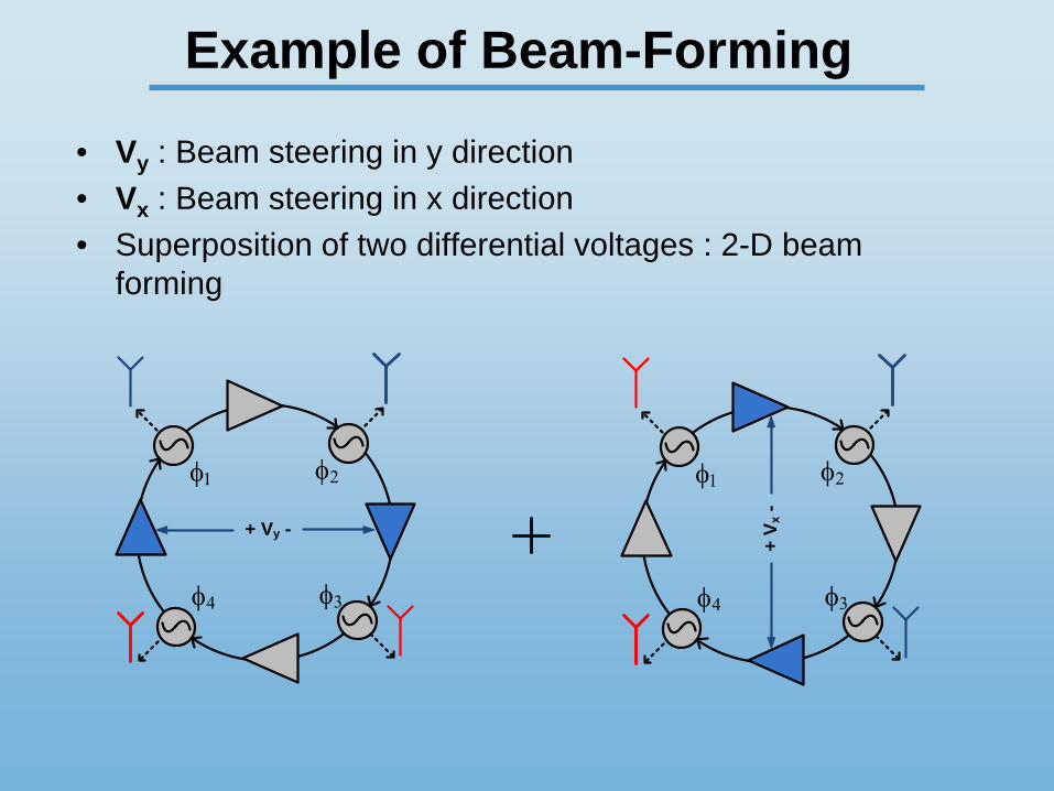
Example of Beam-Forming
• Vy : Beam steering in y direction • Vx : Beam steering in x direction • Superposition of two differential voltages : 2-D beam
forming
φ2φ1
φ3φ4
+ Vy -
φ2φ1
φ3φ4
+ V x
-

Scalable Architectures
• Scalability and stability
• Coupling topology
• 2-D beam forming
• Frequency tuning
0.5
0.5
0.5
0.5
0.5
0.5 0.5
0.5
0.5
0.50.5
0.50.5
0.5
0.5
0.5
1
1
1
1
1
1
1
1
0.5
0.5
0.5
0.5
0.5
0.5 0.5
0.5
0.5
0.50.5
0.50.5
0.5
0.5
0.5
1
1
1
1
1
1
1
1
-Vx
+Vx
+Vy -Vy

A 4x4 Terahertz Phased Array
Chip fabricated in a CMOS 65nm GP bulk process. Simulation results
– Center frequency: 350 GHz – Tuning range: 8% – Generated power: 3.2 mW – Radiated power: 1.4 mW – EIRP > 100 mW
2-D beam forming Highly scalable No global routing

260-GHz Broadband Array
90°
180°
270°
0°
180°
270°
0°
90°
270°
90°
180°
270°
180°
90°
0°
S/W
0°
S/W
DPG
DPG
DPG
DPG
S/W
S/W
2f0
2f0
f0
DPG Digital Pulse Generator
S/W Varactor-Based Switch
QuadratureOscillator
High-Power Oscillator
Integrated Slot Antenna

260-GHz Broadband Array

260-GHz Broadband Array
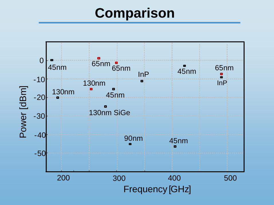
Comparison Po
wer
[dB
m]
200 300
0
Frequency [GHz]
-10
-20
-30
-40
-50
90nm
400
45nm
130nm130nm
500
65nm
130nm SiGe
InP
45nm
InP
45nm45nm 65nm65nm
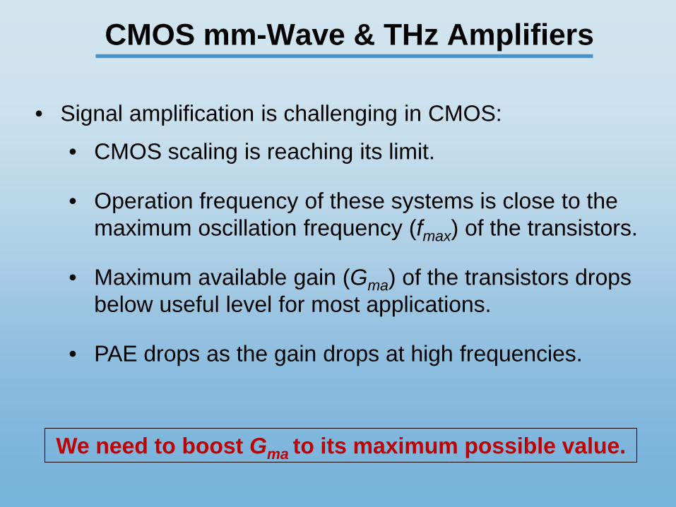
CMOS mm-Wave & THz Amplifiers
• Signal amplification is challenging in CMOS:
• CMOS scaling is reaching its limit.
• Operation frequency of these systems is close to the maximum oscillation frequency (fmax) of the transistors.
• Maximum available gain (Gma) of the transistors drops below useful level for most applications.
• PAE drops as the gain drops at high frequencies.
We need to boost Gma to its maximum possible value.

Optimum Conditions
Gain is maximized by providing optimum voltage gain and phase conditions for the device.
Assuming most of the input power flows from source to port 1 of the device and most of the output power flows to the load:
))(cos()(21 21122112222
1111
ϕ++∠+−+−+≅ ∗∗ YYYYAGAGG
Gain
)()12( *2112 YYkopt +∠−+= πϕ
22
2112
2||
GYYAopt
∗+=

Chip Photo
780 µm
460 µm
Vdd
VoutVin
GND
• Inductors are implemented using microstrip transmission lines.
• Capacitors are implemented using metal finger capacitors or the capacitance pads.

S-Parameter Measurement
• Power gain of 12.5 dB is achieved at 107 GHz. • Input and output reflection coefficients are -13 dB and
-19 dB, respectively. • DC power consumption is 31 mW.
|S-p
aram
eter
| (dB
)
Frequency (GHz) 90 95 100 105 110-30
-20
-10
0
10
20
S22 S12
S11
S21
Outline
• Motivation
• Terahertz Frequency Multipliers
• High Power Terahertz Oscillator Design
• A High Power THz VCO
• THz Radiator Arrays
• Conclusion

Summary
• It is critical to have a good device understanding to squeeze
out the maximum power/gain
• E/M modeling is critical
• Built-in self test is highly desirable
• RF engineers need to learn more microwave/device physics
• For some applications CMOS is not sufficient and compound
semiconductors (especially GaN) show great potential.

Ehsan Afshari Cornell University
(http://unic.ece.cornell.edu)
November 2012
The Next Frontier for Circuit Designers: CMOS THz Systems


![Project: IEEE 802.15 Working Group for Wireless Personal Area Networks (WPANs) Submission Title: [IEEE 802.15 Report at BT Decvon] Date Submitted: [09july00]](https://img.dokumen.tips/doc/110x75/5514b766550346f06e8b6521/project-ieee-80215-working-group-for-wireless-personal-area-networks-wpans-submission-title-ieee-80215-report-at-bt-decvon-date-submitted-09july00.jpg)