Embed Size (px)
Citation preview

Novel Automated Software System for Arcing Simulation inSpacecraft on-Board Electronics
V. Kozhevnikov1, V. Karaban2, D. Kosov2, A. Kozyrev1, A. Batrakov1, N. Semeniuk1, L. Zjulkova1
1Institute of High Current Electronics, Tomsk, Russia2Tomsk State University of Control Systems and Radioelectronics, Tomsk, Russia
Abstract
In our project, we propose an innovative software solution to the problem of electricalarcing risk prediction in high-voltage on-board electronic equipment intended for long-term self-contained use, like spacecraft conditions. As modern on board equipment is notvacuumed the appearance of arcing leads to considerable damages due to high energeticoutput from arcs. In spacecraft, this problem has been current since 1995 when BoeingSatellite Systems offered the BSS 702 platform with high-voltage bus connected to 100 Vstabilized power source. Possible further increase of operating voltages (e.g. due changein standard) will only escalate the problem.
Arcing simulation is a monumental challenge because it represents an attempt ofnumerical solution to the multiscale discharge plasma problem. The main trouble is thatseveral small regions of possible arcing at large PCB location require incredible computerperformance. The newest entry in this field is the decomposition approach [1, 2]. Here wepropose the software implementation for it. The major effort aims to locate potentiallyvulnerable regions for complex electronics. Our software allows analyzing various regimesof arcing w.r.t. multiple parameters changes.
We implement the computational methodology in the Application Builder of the COMSOLMultiphysics® software and AC/DC Module, Plasma Module and CAD Import Module. Ourdesigned software consists of "Three-dimensional macro-model" and "Processing core"modules. Simulation starts with "Three dimensional macro-model" providing necessarypreprocessing as internal definition/import of device geometry from CAD software,definition of operating parameters, grid meshing, imposition of boundary conditions, etc.PCB layout import is carried out from an electrical computer-aided design system in .PCBformat (ASCII). We implement our own data import module using Application Builder toextend import capabilities. Importing of basic 3D geometric structures is available in STEP,IGES, Parasolid®, ACIS®, Inventor®, PTC® Creo® Parametric™, and SOLIDWORKS®formats.
"Processing core" module performs main computations separated into followingsequential steps:1. Electrostatic problem solution for complete device to identify specific field enhancementregions or probable PCB defects (so called "critical regions");

2. Automatic decomposition of the geometrical model from 3D into set of simplified 2Dmodels of critical regions;3. DC-discharge simulation for each critical region with parametric sweep by a set ofparameters (pressure, initial ionization, emission, etc.)
The novel computational algorithm implemented in our software significantly (ten times ascompared to full-scale simulation for particular case) reduces computation cost. It makespossible to solve large diagnostic routines without high performance computing. Theeffectiveness is based on the dimensionality reduction that turns large-scale 3D-simulation into limited set of fast 2D simulations. The majority of pre- and post-processingoperations are automated in order to simplify diagnostics to end user. As a result ofcomputations we obtain the locations of possible electric arcs (critical regions) and criticalranges of operating parameters. Our working prototype can be easily applied todiagnostics of electronic devices operated under wide range of parameters.
Reference
[1] V. Yu. Kozhevnikov et al., Design and Diagnostics of Arc-resistant Electronics for SatelliteTelecommunication Systems, 18th Mediterranean Electrotechnical Conference MELECON2016, Limassol, Cyprus, p. 1 (2016)[2] V. Yu. Kozhevnikov et al., Diagnostics of Primary Arcing in Electronics of SatelliteTelecommunication Systems, 23th Telecommunications forum TELFOR 2015, Belgrade,Serbia, p. 615 (2015) [3] S. A. Onischenko et al., Influence of a Thin Dielectric Film on Electrical Insulation inVacuum Gaps at the Pulse Voltage, 2014 International Symposium on Discharges andElectrical Insulation in Vacuum (ISDEIV), Mumbai, India, p. 49 (2014)[4] A. V. Kozyrev et al., Theoretical Simulation of a Gas Breakdown Initiated by ExternalPlasma Source in the Gap With Combined Metal-Dielectric Electrodes, IEEE Transactionson Plasma Science, Vol. 43, p. 2294, (2015)
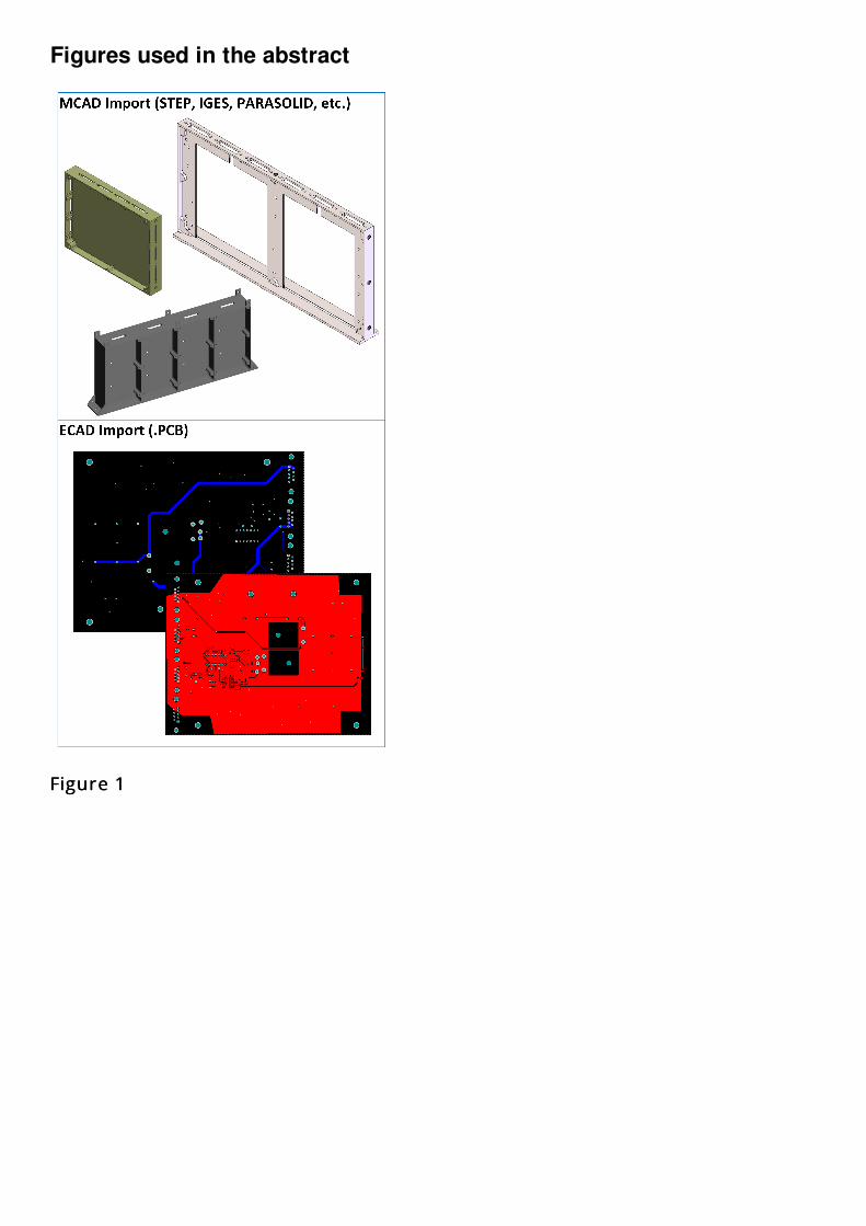
Figures used in the abstract
Figure 1Figure 1

Figure 2Figure 2
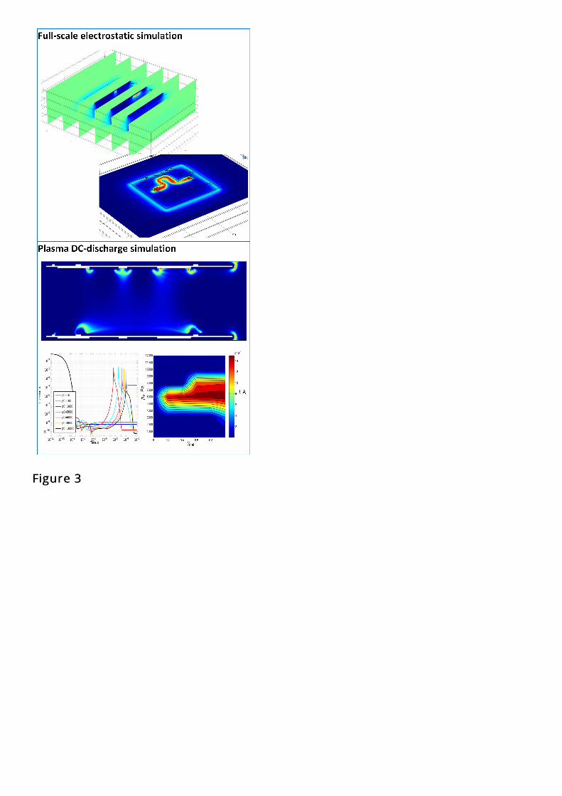
Figure 3Figure 3