Embed Size (px)
Citation preview
NIS5132 Document number: DS36457 Rev. 5 - 3
1 of 12 www.diodes.com
May 2017 © Diodes Incorporated
NIS5132
NOT RECOMMENDED FOR NEW DESIGN NO ALTERNATE PART
2 2
7
9
3.6A 12V RESETTABLE ELECTRONIC FUSE
Description The NIS5132 is a self-protected resettable electronic fuse designed
for consumer applications such as hard disk drives, to industrial
applications to enhance system reliability against catastrophic and
shutdown failures.
Pin Assignments
(Top View)
To support a wide range of demanding applications, the design has
been optimized to operate over the supply range of 9.0V to 18V. For
robustness and protections, the device integrates a low RDS(ON)
NMOS buffer power device along with an undervoltage lockout,
overvoltage clamp, a current limit, a dv/dt control and a thermal
shutdown circuits. The overvoltage circuit limits the output voltage
without shutting the device down to allow the load to continue
operating during over voltage. Thermal shutdown can be either
latching type (NIS5132MN1) or auto-retry type (NIS5132MN2).
Features
9.0 to 18V Operating Input Voltage
GND 1
dv/dt 2
Enable/Fault 3
ILIMIT 4
NC 5
Applications
Hard Drives
10
9
NIS5132MN1 8
NIS5132MN2
7
6
U-DFN3030-10
Source
Source
Source
Source
Source
Integrated NMOS Power Device with RDS(ON) of 30mΩ Typical
Internal Current Limit - No External Current Sense Resistor in
Load Path
Under Voltage Lockout
Over Voltage Clamp (NIS5132MN1 and NIS5132MN2)
Thermal Shutdown
-40C to +150C Operating Junction Temperature
ESD Ratings: HBM > 1500V; MM 200V
Small Low Profile U-DFN3030-10 Package
UL Recognized, Report E322375-20140529
Lead-Free Finish; RoHS Compliant (Notes 1 & 2)
Halogen and Antimony Free. “Green” Device (Note 3)
Mother Board Power Management
Printer Load Power Management
Notes: 1. EU Directive 2002/95/EC (RoHS) & 2011/65/EU (RoHS 2) compliant. All applicable RoHS exemptions applied. 2. See http://www.diodes.com/quality/lead_free.html for more information about Diodes Incorporated’s definitions of Halogen- and Antimony-free, "Green" and Lead-free. 3. Halogen- and Antimony-free "Green” products are defined as those which contain <900ppm bromine, <900ppm chlorine (<1500ppm total Br + Cl) and <1000ppm antimony compounds.
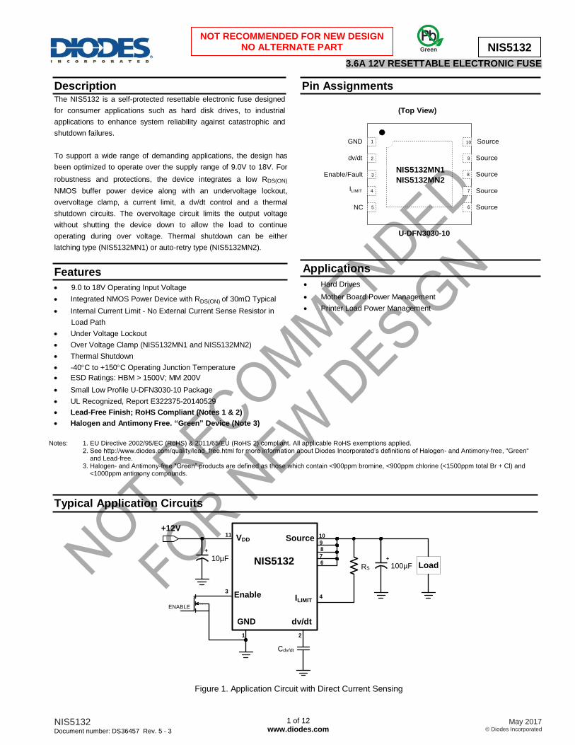
Typical Application Circuits
+12V 11 VDD
+
10µF
Source 10
8
NIS5132 6
+
RS 100µF
Load
ENABLE
3 Enable
GND
ILIMIT 4
dv/dt
1 2
Cdv/dt
Figure 1. Application Circuit with Direct Current Sensing
Green

NIS5132 Document number: DS36457 Rev. 5 - 3
2 of 12 www.diodes.com
May 2017 © Diodes Incorporated
NIS5132
NOT RECOMMENDED FOR NEW DESIGN NO ALTERNATE PART
7
2
5V
9
9
Typical Application Circuits (Cont.)
+12V 11 VDD
+
10µF
Source 10
8
NIS5132 6
+
100µF
Load
ENABLE
3
Enable
GND
RS
ILIMIT 4
dv/dt
1 2
Cdv/dt
Figure 2. Application Circuit with Kelvin Current Sensing
1 Source
3
VDD 11 12V
11 VDD
Source 10
8 7
Load
COUT
RS
4
5
7 ILIMIT
NIS5135
8
Enabe
CIN CIN NIS5132
3
Enable
6
4
ILIMIT
RS C
OUT
Load
dv/dt
GND
ENABLE
GND
dv/dt
9 10
Cdv/dt
1 2
Cdv/dt
Figure 3. Application Circuit with Common Thermal Shutdown
Pin Descriptions
Package: U-DFN3030-10
Pin Number Pin Name Function
1 GND Ground pin
2
dv/dt
Internal NMOS power device turn-on time adjustment pin:
If this pin is left unconnected, the internal capacitor ensures the turn-on ramp is over a period of 2ms typical. If an additional delay is required, connect a capacitor from this pin to the ground.
3
Enable/Fault
Tri-state bi-directional interface pin:
The output can be disabled by pulling this pin to ground through an open drain or an open collector. Additionally, this pin output goes to an intermediate state to indicate that the device is in thermal shutdown state. This pin can also be connected together with other NIS5132 devices to cause a system-wide simultaneous shutdown during thermal events.
4
ILIMIT
Current limit setting pin:
A resistor between Source pins and this pin sets the overload and short-circuit current limit thresholds.
5 NC No connection
6 to 10
Source
The internal NMOS power device’s Source pins:
These pins are the Source of internal power device and also the output terminal of the electronic fuse
Exposed PAD VDD Positive input voltage to the device

NIS5132 Document number: DS36457 Rev. 5 - 3
3 of 12 www.diodes.com
May 2017 © Diodes Incorporated
NIS5132
NOT RECOMMENDED FOR NEW DESIGN NO ALTERNATE PART
Functional Block Diagram
Enable/ Fault
Enable Charge Pump
Source
Thermal
Shutdown
UVLO Voltage Clamp
Current Limit
dv/dt Control
ILIMIT
dv/dt
Figure 4. Block Diagram
GND
Enable/Fault
4.3V
12µA
1.4V
SD
Startup
Blanking
Thermal
2.64V
0.58V
+
-
-
+
Thermal Reset
Enable SD
Shutdown
Thermal SD
Figure 5. Enable/Fault Function Circuit
VDD

NIS5132 Document number: DS36457 Rev. 5 - 3
4 of 12 www.diodes.com
May 2017 © Diodes Incorporated
NIS5132
NOT RECOMMENDED FOR NEW DESIGN NO ALTERNATE PART
Absolute Maximum Ratings (Note 4) (@TA = +25°C, unless otherwise specified.)
Symbol Characteristic Value Unit
VDD
Input Voltage in Steady State Operating Conditions (Note 5) -0.6 to +18
V Input Voltage - Transient (100ms) -0.6 to +25
JA
Junction to Air Thermal Resistance 0.1 in2 (Note 6) 227
°C/W
0.5 in2 (Note 6) 95
JL Junction to Lead Thermal Resistance 27
JC Junction to Case Thermal Resistance 20
PDMAX Package Power Dissipation at TA= +25°C 1.3 W
— Thermal Derating Above +25°C 10.4 mW/°C
TS Storage Temperature Range -55 to +155 °C
TJ Operating Junction Temperature (Note 7) -40 to +150 °C
TL Lead Temperature During Soldering (10s) +260 °C
Notes: 4.Stresses greater than the 'Absolute Maximum Ratings' specified above may cause permanent damage to the device. These are stress ratings only; functional operation of the device at these or any other conditions exceeding those indicated in this specification is not implied. Device reliability may be affected by exposure to absolute maximum rating conditions for extended periods of time. 5. Negative voltage will not damage the device provided that the power dissipation is within the package dissipation rating. 6. 1 oz copper on double sided FR-4 PCB. 7. Thermal limit is set above the maximum thermal rating. It is not recommended to operate the device at temperature above the maximum rating for extended period.
Recommended Operating Conditions
Symbol Characteristic Test Condition Rating Unit
VDD Supply Voltage Operating 9.0 to 18.0 V
TJ Operating Junction Temperature Range Operating -40 to +150 °C

NIS5132 Document number: DS36457 Rev. 5 - 3
5 of 12 www.diodes.com
May 2017 © Diodes Incorporated
NIS5132
NOT RECOMMENDED FOR NEW DESIGN NO ALTERNATE PART
Electrical Characteristics (VDD = 12V, CL = 100µF, dv/dt pin open, RLIMIT = 10Ω, and TA = +25°C, unless otherwise noted.)
Symbol Characteristic Test Condition Min Typ Max Unit
Device
IBIAS Bias Current Device operational — 0.8 1.5 mA
IBIAS_SD Bias Current During Shutdown Device shutdown — 0.4 — mA
VDD_MIN Minimum Operating Voltage Once
Successfully Started Up — — — 7.6 V
NMOS Power Device
tDLY Chip Enable Delay Time Enabling of the IC to ID = 100mA
(with 1A resistive load) — 220 — µs
RDS(ON) NMOS Drain to Source Kelvin ON
Resistance (Note 8)
NMOS fully on 20 30 40 mΩ
NMOS fully on, TJ = +140°C — 45 —
VOUT_OFF Off State Output Voltage VDD = 18V, VGS = 0V, RL = ∞ — 0.19 0.3 V
ID Continuous Current (Note 9) TA = +25°C, 0.5 in.
2 pad — 3.6 —
A TA = +80°C, min copper — 1.7 —
— Output Capacitance VDS = 12V, VGS = 0V, f = 1MHz — 250 — pF
dv/dt Ramp
tSLEW Output Voltage Ramp Time Device enable to VDS = 11.7V 1.5 1.8 2.5 ms
VC_MAX Maximum Capacitor Voltage — — — VDD V
Under/Over Voltage Protection
VUVLO Undervoltage Lockout Threshold Turn on, Voltage rising 7.7 8.5 9.3 V
VUVLO_HYST Undervoltage Lockout Hysteresis — — 0.80 — V
VCLAMP Overvoltage Clamp Limit (Note 10) During overvoltage protection,
VDD = 18V 14 15 16.2 V
Current Limit
ILIMIT_SS Kelvin Short Circuit Current Limit
(Note 11) RLIMIT = 15.4Ω 2.75 3.44 4.25 A
ILIMIT_OL Kelvin over Load Current Limit
(Note 11) RLIMIT = 15.4Ω 3.5 4.6 6.0 A
Thermal Protection
TSD Thermal Shutdown Junction Temperature
Threshold (Note 9) Temperature rising +150 +175 +200 C
TSD_HYST Thermal Shutdown Hysteresis in Non
Latching Devices — — +45 — C
Enable/Fault
VEN_LOW Enable Logic Level Low Voltage Output disabled 0.35 0.58 0.81 V
VEN_MID Enable Logic Level Mid Voltage Output disabled, Thermal fault 0.82 1.4 1.95 V
VEN_HI Enable Logic Level High Output enabled 1.96 2.64 3.3 V
VEN_MAX High State Maximum Voltage — 3.4 4.3 5.3 V
IEN_SINK Logic Low Sink Current VENABLE = 0V — -17 -25 µA
IEN_LKG Logic High Leakage Current for External
Switch VENABLE = 3.3V — — 1.0 µA
Fanout
Maximum Fanout – Number of Device
that can be Connected Together to this
Pin for Simultaneous Shutdown
— — — 3.0 Units
Notes: 8. Pulse test with pulse width of 300µs, duty cycle 2%. 9. This parameter is not tested in production. It is guaranteed by design, process control and characterization. 10. Over voltage clamp feature is available on in NIS5132MN1 and NIS5132MN2 versions. 11. Refer to application note on explanation on short circuit and overload conditions.

NIS5132 Document number: DS36457 Rev. 5 - 3
6 of 12 www.diodes.com
May 2017 © Diodes Incorporated
NIS5132
NOT RECOMMENDED FOR NEW DESIGN NO ALTERNATE PART
Volt
age
(V)
Volt
age
(V)
Cu
rren
t (A
) H
YS
T (
V)
Performance Characteristics
9 0.88
8.8
0.86
8.6
8.4
8.2
8
7.8
7.6
0.84
0.82
0.8
0.78
0.76
7.4
-50 -25 0 25 50 75 100 125 150
Temperature (oC)
0.74
-50 -25 0 25 50 75 100 125 150
Temperature (oC)
Figure 6. UVLO Turn-On Voltage vs. Temperature Figure 7. UVLO Hysteresis vs. Temperature
15.3
15.2
15.1
15
14.9
14.8
14.7
14.6
14.5
-50 -25 0 25 50 75 100 125 150
Temperature (oC)
(oC)
Figure 8. Output Clamp Voltage vs. Temperature Figure 9. Output Voltage dv/dt Ramp Time vs. Temperature
Figure 10. Input Transient Response
1.80
1.60
1.40
1.20
1.00
0.80
0.60
0.40
0.20
0.00
400.00 500.00 600.00 700.00 800.00 900.00 1000.00
Forward Voltage (V)
Figure 11. Body Diodes Forward Characteristics

NIS5132 Document number: DS36457 Rev. 5 - 3
7 of 12 www.diodes.com
May 2017 © Diodes Incorporated
NIS5132
NOT RECOMMENDED FOR NEW DESIGN NO ALTERNATE PART
On
R
esis
tan
ce (
m
)
Cu
rren
t (A
) C
urr
ent
(A)
Cu
rren
t (A
) C
urr
ent
(A)
Cu
rren
t (A
)
Performance Characteristics (Cont.)
35 10
32.5
30
OL
SC 27.5 1
25
22.5
20
7 8 9 10 11 12 13 14 15
VCC (V)
0.1
10 100 1000
RSENSE ( )
Figure 12. Power Device ON Resistance (RDS(ON)) vs. VCC Figure 13. Current Limit vs. RSENSE for Direct Current
Sensing
10
4.5
4
3.5
3
2.5
2
1.5
1
1
OL OL
SC SC
0.5
0
-50 -30 -10 10 30 50 70 90
Temperature (oC)
Figure 14. Direct Current Sensing Level vs. Temperature
(RSENSE = 27Ω)
0.1
1 10 100
RLIMIT ()
Figure 15. Current Limit vs. RSENSE for Kelvin Current
Sensing
6 4
5.5
5
3.5
OL
SC 3
4.5 2.5
4
3.5
2
OL
1.5 SC
3
-40 -20 0 20 40 60 80 100
Temperature (oC)
1
-40 -20 0 20 40 60 80 100
Temperature (oC)
Figure 16. Kelvin Current Sensing Levels vs.
Temperature (RSENSE = 15)
Figure 17. Kelvin Current Sensing Levels vs. Temperature
(RSENSE = 33Ω

NIS5132 Document number: DS36457 Rev. 5 - 3
8 of 12 www.diodes.com
May 2017 © Diodes Incorporated
NIS5132
NOT RECOMMENDED FOR NEW DESIGN NO ALTERNATE PART
Application Note
Theory of Operation
The NIS5132 is a self-protected, resettable electronic fuse. It monitors the input and output voltage, the output current and the die temperature.
When the NIS5132 is powered up it will ramp up the output voltage based on the dv/dt setting (see description below) and current will begin to flow.
The device current limit can be set with an external resistor, the ramp rate (dv/dt) can be adjusted with an external capacitor. The Overvoltage
Clamp, Undervoltage Lockout and Thermal Protection are internally set.
Power Supply Considerations
Placing a high-value electrolytic capacitor or X7R (X5R) ceramic capacitor between VDD to GND (10µF) and Source to GND (100µF) as close to
the device as possible is highly recommended. This precaution reduces power-supply transients that may cause ringing on the input and load
transients that may cause output voltage falls below input voltage resulting device over-heat.
Current Limit
The NIS5132 incorporates a sensefet with a reference and amplifier to control the current in the device. The sensefet uses a small fraction of the
load current to measure the actual current. This reduces the losses as a smaller sense resistor can be used. The current can be measured direct
with the Rs resistor connected between the load and the ILIMIT pin (see Figure 1). That method includes the resistance of the bond wires in the
current limiting circuit. Or a Kelvin connection (see Figure 2) can be used, in that case one of the 5 source pins will be used and the voltage is
measured on the die eliminating the bond wire resistance. That reduces the source pins to the load to four and with that increases the on
resistance of the effuse to the load.
Overvoltage Clamp
The NIS5132MN1 and NIS5132MN2 monitor the input voltage and clamp it once it exceeds 15V. This will allow for transient on the input for short
periods of time. If the input voltage stays above 15V for extended time the voltage drop across the FET with the load current will increase the die
temperature and the thermal shutdown feature will protect the device and shut it down.
Undervoltage Lock Out
The input voltage of the NIS5132 is monitored by an UVLO circuit (undervoltage lockout) if the input voltage drops below this threshold the output
transistor will be pulled into a high impedance state.
dv/dt
The NIS5132 has an integrated control circuit that forces a linear ramp on the output voltage raise regardless of the load impedance. Without
connecting a capacitor on the dv/dt pin the ramp time is roughly 2ms. Adding an external capacitor can increase this ramp rate. The internal
current source of 90µA will charge the external capacitor at a slow rate. It is recommended to utilize a ceramic capacitor.
The ramp time can be determined with the following equation
Cext in Farad
tramp in seconds
The ramp up circuit is discharged and VOUT starts from 0V when the units shut down after a fault, enable shutdown or input power cycle.
Enable/Fault
The NIS5132 has a tri state Enable/Fault pin. It is used to turn on and off the device with high and low signals from a GPIO, but can also indicate a
thermal fault. When the Enable/Fault pin is pulled low the output is turned off, when the Enable/Fault pin is pulled high the output is turned on. In
the event of a thermal fault the Enable/Fault pin will be pulled low to an intermediate voltage by an internal circuit. This can be used to chain up to
4 NIS5132 together that during a thermal shut down the linked devices turn off as well.
Due to this fault indication capability it should not be connected to any type of logic with an internal pull up device.
The NIS5132MN1 connected to a 2
nd device will latch-off until the Enable/Fault pin has been pulled to low and then allowed to go back up to a high
signal, or if the power has been cycled. Once the part starts up again it will go through the startup ramp determined by the internal circuit or based
on the externally connected capacitor on pin dv/dt.
The MN2 devices will auto restart once the part that indicated a thermal shutdown has cooled down. It will also go through the startup ramp.

NIS5132 Document number: DS36457 Rev. 5 - 3
9 of 12 www.diodes.com
May 2017 © Diodes Incorporated
NIS5132
NOT RECOMMENDED FOR NEW DESIGN NO ALTERNATE PART
Application Note (Cont.)
Enable/Fault (Cont.)
Figure 18. Enable/Fault Signal Levels
Thermal Protection
The NIS5132 has an integrated temperature sensing circuit that protects the die in the event of over temperature. The trip point has been
intentionally set high at +175˚C to allow for increase trip time during high power transient events. The NIS5132 will shut down current flow to the
output when the die temperature reaches +175°C. The NIS5132MN1 will restart after the Enable pin has been toggled or the input power has
been cycled. The NIS5132MN2 will auto restart after the die temperature has been reduced by -45°C.
Even that the thermal trip point has been set high to allow for high current transients the circuit design should accomplish best thermal
performance with good thermal layout of the PCB. It is not recommended to operate NIS5132 above +150°C over extended periods of time.
Ordering Information
NIS5132 XXX - XXX - 7
PackingPackage
FN : U-DFN3030-10 7 : Tape & Reel
Feature Option
MN1 : Thermal latching with VCLAMP
MN2 : Thermal auto-retry with VCLAMP
Part Number Package
Code Packaging
7” Tape and Reel
Quantity Part Number Suffix
NIS5132MN1-FN-7 FN U-DFN3030-10 3,000/Tape & Reel -7
NIS5132MN2-FN-7 FN U-DFN3030-10 3,000/Tape & Reel -7

NIS5132 Document number: DS36457 Rev. 5 - 3
10 of 12 www.diodes.com
May 2017 © Diodes Incorporated
NIS5132
NOT RECOMMENDED FOR NEW DESIGN NO ALTERNATE PART
Marking Information
(1) Package Type: U-DFN3030-10
( Top View )
XX Y : Year : 0~9
X : A~Z : Internal code
XX : Identification Code
W : Week : A~Z : 1~26 week;
a~z : 27~52 week; z represents52 and 53 week
Y W X
Part Number Package Identification Code
NIS5132MN1 U-DFN3030-10 M2
NIS5132MN2 U-DFN3030-10 N2
Package Outline Dimensions Please see http://www.diodes.com/package-outlines.html for the latest version.
U-DFN3030-10
U-DFN3030-10
Dim Min Max Typ
A 0.57 0.63 0.60
A1 0 0.05 0.02
A3 - - 0.15
b 0.20 0.30 0.25
D 2.90 3.10 3.00
D2 2.30 2.50 2.40
e - - 0.50
E 2.90 3.10 3.00
E2 1.50 1.70 1.60
L 0.25 0.55 0.40
z - - 0.375
All Dimensions in mm
Suggested Pad Layout Please see http://www.diodes.com/package-outlines.html for the latest version. U-DFN3030-10
Dimensions Value (in mm)
Z 2.60
G 0.15
X 1.80
X1 0.60
Y 0.30
C 0.50
SEATING PLANE
A3A
A1
Pin#1 ID
L
E E2
DD2
bez
CY
Z
X
X1
G
G

NIS5132 Document number: DS36457 Rev. 5 - 3
11 of 12 www.diodes.com
May 2017 © Diodes Incorporated
NIS5132
NOT RECOMMENDED FOR NEW DESIGN NO ALTERNATE PART
Taping Orientation
(1) Package Type: U-DFN3030-10
Note: 12. The taping orientation of the other package type can be found on our website at http://www.diodes.com/datasheets/ap02007.pdf.

NIS5132 Document number: DS36457 Rev. 5 - 3
12 of 12 www.diodes.com
May 2017 © Diodes Incorporated
NIS5132
NOT RECOMMENDED FOR NEW DESIGN NO ALTERNATE PART
IMPORTANT NOTICE DIODES INCORPORATED MAKES NO WARRANTY OF ANY KIND, EXPRESS OR IMPLIED, WITH REGARDS TO THIS DOCUMENT, INCLUDING, BUT NOT LIMITED TO, THE IMPLIED WARRANTIES OF MERCHANTABILITY AND FITNESS FOR A PARTICULAR PURPOSE (AND THEIR EQUIVALENTS UNDER THE LAWS OF ANY JURISDICTION). Diodes Incorporated and its subsidiaries reserve the right to make modifications, enhancements, improvements, corrections or other changes without further notice to this document and any product described herein. Diodes Incorporated does not assume any liability arising out of the application or use of this document or any product described herein; neither does Diodes Incorporated convey any license under its patent or trademark rights, nor the rights of others. Any Customer or user of this document or products described herein in such applications shall assume all risks of such use and will agree to hold Diodes Incorporated and all the companies whose products are represented on Diodes Incorporated website, harmless against all damages. Diodes Incorporated does not warrant or accept any liability whatsoever in respect of any products purchased through unauthorized sales channel. Should Customers purchase or use Diodes Incorporated products for any unintended or unauthorized application, Customers shall indemnify and hold Diodes Incorporated and its representatives harmless against all claims, damages, expenses, and attorney fees arising out of, directly or indirectly, any claim of personal injury or death associated with such unintended or unauthorized application. Products described herein may be covered by one or more United States, international or foreign patents pending. Product names and markings noted herein may also be covered by one or more United States, international or foreign trademarks. This document is written in English but may be translated into multiple languages for reference. Only the English version of this document is the final and determinative format released by Diodes Incorporated.
LIFE SUPPORT Diodes Incorporated products are specifically not authorized for use as critical components in life support devices or systems without the express written approval of the Chief Executive Officer of Diodes Incorporated. As used herein: A. Life support devices or systems are devices or systems which: 1. are intended to implant into the body, or
2. support or sustain life and whose failure to perform when properly used in accordance with instructions for use provided in the labeling can be reasonably expected to result in significant injury to the user.
B. A critical component is any component in a life support device or system whose failure to perform can be reasonably expected to cause the failure of the life support device or to affect its safety or effectiveness. Customers represent that they have all necessary expertise in the safety and regulatory ramifications of their life support devices or systems, and acknowledge and agree that they are solely responsible for all legal, regulatory and safety-related requirements concerning their products and any use of Diodes Incorporated products in such safety-critical, life support devices or systems, notwithstanding any devices- or systems-related information or support that may be provided by Diodes Incorporated. Further, Customers must fully indemnify Diodes Incorporated and its representatives against any damages arising out of the use of Diodes Incorporated products in such safety-critical, life support devices or systems. Copyright © 2017, Diodes Incorporated www.diodes.com