Embed Size (px)
Citation preview

Northwestern University, Dept. of ECE, Technical Report, 1996.
Software Technologies for Reconfigurable SystemsScott Hauck Anant AgarwalDepartment of ECE Department of EECSNorthwestern University Massachusetts Institute of TechnologyEvanston, IL 60208 USA Cambridge, MA 02139 [email protected] [email protected]
Abstract
FPGA-based systems are a significant area of computing, providing a high-performance implementationsubstrate for many different applications. However, the key to harnessing their power for most domainsis developing mapping tools for automatically transforming a circuit or algorithm into a configuration forthe system. In this paper we review the current state-of-the-art in mapping tools for FPGA-basedsystems, including single-chip and multi-chip mapping algorithms for FPGAs, software support forreconfigurable computing, and tools for run-time reconfigurability. We also discuss the challenges forthe future, pointing out where development is still needed to let reconfigurable systems achieve all oftheir promise.
1.0 Introduction
Reconfigurable computing is becoming a powerful methodology for achieving high-performance implementationsof many applications. By mapping applications into FPGA hardware resources, extremely efficient computationscan be performed. In [Hauck98] we presented numerous reconfigurable systems, and described the varied roles ofthese systems. However, hardware is only one part of a complete system. In order for multi-FPGA systems toachieve widespread use, they not only require an efficient hardware implementation medium, but also a complete,automatic software flow to map circuits or algorithms onto the hardware substrate. Similar to a compiler for astandard programming language, the mapping software for a multi-FPGA system takes in a description of thecircuit to be implemented, and through a series of transformations creates an implementation of the circuit in thebasic primitives of the hardware system. In a multi-FPGA system, this implementation is programming files orbitstreams for the FPGAs in the system.
For the developers and users of reconfigurable systems there is a tradeoff to be made between hand mapping to thesystem, creating high-quality implementations but requiring a very hardware-savvy user, and automatic toolswhich free the user from some implementation details, but which can (sometimes substantially) impact theresulting quality. In this paper we focus primarily on software tools to partially or completely automate themapping process. While these algorithms are still in their infancy, our hope is that they will lead to an efficient,automatic mapping solution for reconfigurable systems. However, it is important to realize that there will alwaysbe a role for hand-mapped implementations, just as in the compiler-dominated world of general-purposecomputing there is still a role for assembly-language programming where the required quality demands the highestperformance implementation possible.
Before we discuss the specific steps necessary to map onto a multi-FPGA system, it is necessary to consider someof the features of a multi-FPGA system that impact this software flow. One of the most important concerns inmulti-FPGA systems is that while the FPGAs are reprogrammable, the connections between the FPGAs are fixedby traces on the circuit board. Thus, not all FPGAs may be interconnected, and communication between FPGAsmust be carried on these limited resources. If the source and destination of a route are on different FPGAs, and theFPGAs are not directly connected, this signal will need to traverse one or more intermediate FPGAs. This addsextra delay to the routing, and uses up multiple FPGA I/O pins. This latter constraint can be the major bottleneckin multi-FPGA systems, with I/O resource constraints in some cases (especially logic emulation) limiting achievedlogic utilization of FPGAs to 10%-20%. Thus, the primary concern of mapping tools for a multi-FPGA system islimiting the amount of I/O resources needed by a mapping. Not only does this mean that most signals should bekept within a single FPGA, but also that those signals that need to be communicated between FPGAs should becommunicated between neighboring FPGAs. Thus, the mapping tools need to understand the topology of themulti-FPGA system, and must optimize the mapping to fit within this routing topology. Note that some topologies
2
use crossbars or FPICs1, devices meant to ease this I/O bottleneck. However, even these chips have finite I/Oresources, and the connections between them and the FPGAs are fixed. Thus the restrictions of a fixed topologyoccur even in these systems.
Not only must the tools optimize to a fixed topology, but in some circumstances they must also be fully automatic.In the case of logic emulation, the user of the system has no desire to learn all the details of a multi-FPGA system,and will be unwilling to hand-optimize their complex design to a multi-FPGA system. The system is meant tospeed time-to-market of the system under validation, and without an automatic mapping solution the speed benefitsof emulation will be swamped by the mapping time and human effort. Also, for a multi-FPGA system targeted togeneral software acceleration, the users of the system will be software programmers, not hardware designers.While there are situations where a hand-optimized solution may be the right answer, for many other domains acomplete, automatic mapping system is a necessity. Merging these two demands together, developing an automaticsystem with the ability to also take user input to partially or completely guide the mapping process will be animportant concern for reconfigurable systems.
Structural Circuit
Description
Programming Files
Logic Restructuring
Partitioning & Global Placement
Global Routing
Pin Assignment
FPGA Routing
FPGA Placement
Tech Mapping
FPGA Routing
FPGA Placement
Tech Mapping
FPGA Routing
FPGA Placement
Tech Mapping
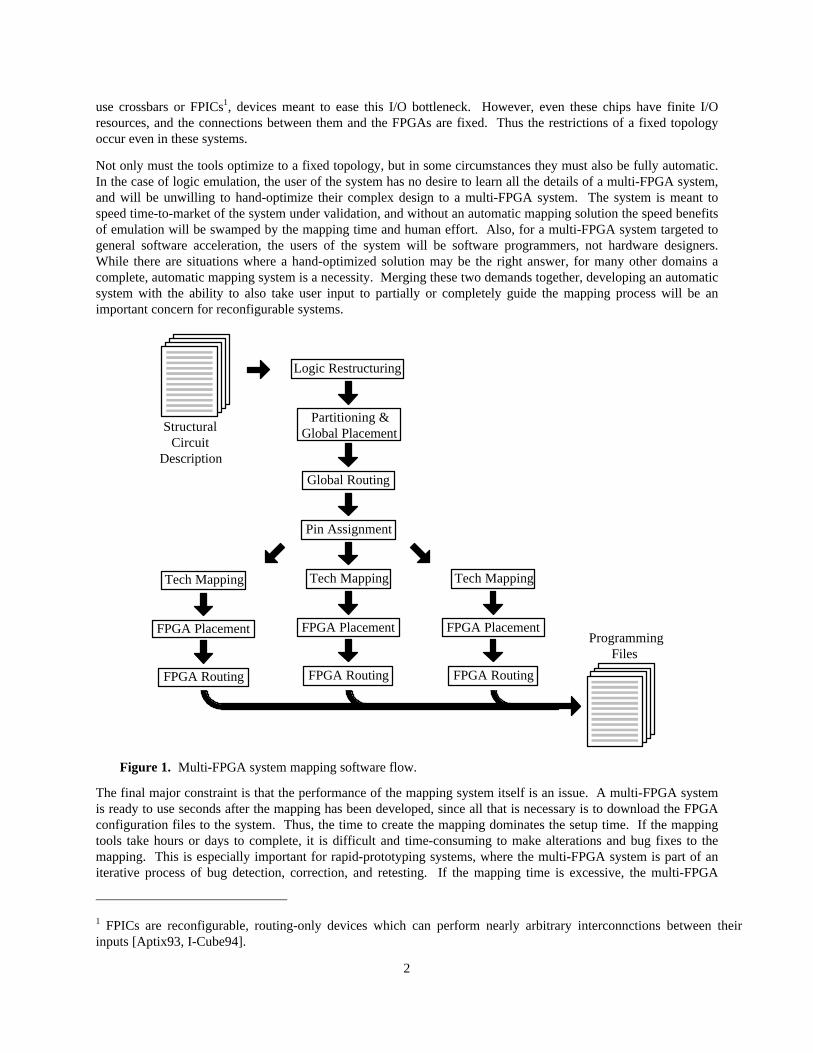
Figure 1. Multi-FPGA system mapping software flow.
The final major constraint is that the performance of the mapping system itself is an issue. A multi-FPGA systemis ready to use seconds after the mapping has been developed, since all that is necessary is to download the FPGAconfiguration files to the system. Thus, the time to create the mapping dominates the setup time. If the mappingtools take hours or days to complete, it is difficult and time-consuming to make alterations and bug fixes to themapping. This is especially important for rapid-prototyping systems, where the multi-FPGA system is part of aniterative process of bug detection, correction, and retesting. If the mapping time is excessive, the multi-FPGA
1 FPICs are reconfigurable, routing-only devices which can perform nearly arbitrary interconnctions between theirinputs [Aptix93, I-Cube94].
3
system will be used relatively late in the design cycle (where bugs are few), which greatly limits their utility. Witha mapping process that takes only minutes, it becomes possible to use the benefits of logic emulation much earlierin the design cycle, increasing the usefulness of a multi-FPGA system.
2.0 Overview
The input to the multi-FPGA mapping software may be a description in a hardware description language such asVerilog or VHDL, a software programming language such as C or C++, or perhaps a structural circuit description.A structural circuit description is simply a representation of a circuit where all the logic is implemented in basicgates (ANDs, ORs, latches, etc.), or in specific, premade parts (i.e., microprocessors, memories, etc.).Programming language descriptions (Verilog, VHDL, C) differ from structural descriptions in that the logic maybe described more abstractly, or “behaviorally”, with the functions described by what needs to be done, not by howit should be implemented. Specifically, an addition operation in a behavioral description would simply say thattwo values are added together to form a third number, while a structural description would state the exact logicgates necessary to perform this computation. To implement the behavioral descriptions, there are automaticmethods for converting such descriptions into structural circuit descriptions. Details of such transformations canbe found elsewhere [McFarland90]. Our discussion of the mapping process starts with structural circuitdescriptions, while sections 5 and 6 will overview methods for handling higher level specifications.
To convert from a structural circuit description to a multi-FPGA realization requires a series of mapping steps(Figure 1). These steps include logic restructuring, partitioning & global placement, global routing, pinassignment, and FPGA technology mapping, placement and routing. FPGA technology mapping, placement androuting are identical to the tools used for single FPGAs. In the pages that follow, we will first give a brief overviewof the process. A more in-depth discussion of each of the steps appears later in this paper.
The first mapping step is logic restructuring. Logic restructuring alters the input netlist so that it can be mapped tothe multi-FPGA system. Asynchronous components and gated clocks may need to be carefully considered orisolated, and RAM usage must be made to fit into the physical RAM chips available in the system.
After logic restructuring, partitioning takes the single input circuit description and splits it into pieces smallenough to fit into the individual FPGAs in the system. The partitioner must ensure not only that the partitions itcreates are small enough to fit the logic capacity of the FPGAs, but must also ensure that the inter-FPGA routingcan be handled within the constraints of the multi-FPGA routing topology. Commonly global placement, theprocess of assigning partitions to specific FPGAs in the system, is combined with the partitioning stage.Otherwise, it is unclear where a given partition resides within the multi-FPGA topology, and thus it can be difficultto properly optimize the interpartition connectivity.
After partitioning and global placement, global routing handles the routing of inter-FPGA signals (i.e., the signalsthat need to be communicated between partitions). This phase can be broken up into abstract global routing anddetailed global routing (pin assignment). Abstract global routing (hereafter referred to simply as global routing)determines through which FPGAs an inter-FPGA signal will be routed. Pin assignment then decides whichspecific I/O pins on each of the FPGAs will carry the inter-FPGA signals.
Once partitioning, global placement, global routing, and pin assignment are completed, all that is left is thetechnology mapping, placement and routing of the individual FPGAs in the system. When these steps arecompleted, there will be configuration files prepared for each FPGA in the system. Downloading these files to themulti-FPGA system then customizes the multi-FPGA system, creating a complete realization of the desiredfunctionality.
In the sections that follow, we will discuss techniques for implementing each of these operations. Section 3 coverssingle-chip mapping tools, reviewing techniques from standard FPGAs for use in reconfigurable systems. Then,section 4 discusses multi-chip tools, showing what techniques are necessary to convert the multi-FPGA mappingproblem into a set of independent single-chip mappings. Finally, we consider tools and techniques specialized forFPGA-based computation, including reconfigurable computing techniques in section 5, and run-time

4
reconfigurability in section 6. We then sum up the paper, providing an overview of current systems, as well as adescription of areas for future innovation.
3.0 Single-Chip Mapping Tools
While some circuits are designed by hand, in many cases automatic mapping software is critical to logicdevelopment. This is particularly true for technologies such as FPGAs, where in general the complete mappingprocess is carried out by mapping software. In the following sections we will discuss some of the most importantsteps in mapping to LUT (lookup-table) based FPGAs. Note that the process is similar, but not identical, for othertypes of FPGAs. First is technology mapping, which restructures the input netlist into the logic blocks of theFPGA. Next, placement decides which specific logic blocks inside the FPGA will contain the logic functionscreated by technology mapping. Finally, routing determines what routing resources inside the FPGA will be usedto carry the signal from where they are generated to where they are used. A more detailed treatment of all of thesetasks can be found elsewhere [Venkateswaran94]. These single-chip FPGA mapping tools provide a method forimplementing arbitrary logic within an FPGA, and form an important part of all mapping methodologies forFPGA-based systems.
3.1 Technology Mapping
The user of an FPGA provides as input a circuit specified as some interconnection of basic logic gates andfunctions. These functions may have more or less inputs than the LUTs in the FPGA that will implement them.When the logic gate has too many inputs, it must be split into smaller functions which can fit inside the LUTs inthe FPGA. If the gates have too few inputs, several interconnected gates could be combined to fit into a singleLUT, decreasing the amount of LUTs needed to handle the mapping. By reducing the number of LUTs, more logiccan be fit in the same sized FPGA, or a smaller FPGA could be used. The process of restructuring the logic to bestfit the logic blocks in an FPGA is called technology mapping.
A B
D E F G H I J K L M N
C X
Y
Z
1
2
3 4
5
9
7
A B
D E
C
F G H
I J K L M N
X
Y
Z
1
2
3 4
5
6
7
8
9
LUT 1
LUT 2
LUT 3
LUT 4
Figure 2. Example of 5-input LUT technology mapping. The input circuit (left) is restructured andgrouped together into 5-input functions (right). The gray loops at right indicate individual LUTs. Thenumbers on the gates are for identification.
There are many different methods and approaches to the technology mapping of circuits for FPGA implementation[Brown92a, Vincentelli93]. An example of this process is shown in Figure 2. The circuit at left is restructured

5
into four 5-input LUTs, designated by the gray loops at right. Some of the logic functions, such as gate 7 at left,have more inputs than the LUT can handle. Thus, the gate will be split (“decomposed”) into two gates (7 and 8 atright). Then, the gates are grouped together (“covered”) into LUTs, while trying to minimize the total number ofLUTs required. Note that this grouping can be complex. For example, even though gates 1 and 3 each have threeinputs, and thus should not fit into a single LUT with gate 2, since input C is shared between the two gates a single5-input LUT can handle all three gates. Finding this reconvergent fanout can be difficult. Also, this groupingprocess can cause the logic to be restructured. For example, gate 5 at left is duplicated, creating gates 5 and 6 atright. Although this seems like it would increase the hardware cost, replicating the logic can actually reduce thelogic cost. In the example shown, if gate 5 was not replicated, it could not be grouped with either of its fanouts,since by grouping a gate with its fanout the gate’s output is no longer available to other functions. However, byduplicating the gate, the duplicates can each be grouped with one of the fanouts, reducing the total LUT count.
Many approaches and optimizations are possible for technology mapping. For example, Chang et al. [Chang96]provides an approach that is capable of optimizing either the number of lookup tables or the latency of the resultingcircuit. Similarly, methods for area and speed optimization are found in [Abouzeid93]. Instead of just mappingfor LUT count, some algorithms optimize for performance or routeability (i.e., how easy it is to route the logicgenerated by technology mapping). Also, real FPGAs usually have logic blocks that are more complex than asingle n-input LUT, and thus require more complex mapping algorithms. Recognizing that the use of LUT-basedfunction units and restricted interconnect requires non-traditional logic synthesis approaches, Hwang et al.[Hwang94] present a logic synthesis technique based on communication complexity analysis. Numerousapproaches to these and other mapping issues are presented in the literature, including work on logicdecomposition [Murgai94, Chen95, Huang95a, Sawada95, Shen95, Stanion95, Wurth95, Legl96], covering[Cong92, Cong93, Farrahi94], and combined approaches [Francis90, Murgai90, Francis91a, Francis91b,Murgai91a, Murgai91b].
1
2 3 4
A
B
C
D
E
F
G H I J K L M N
Figure 3. Placement of the circuit from Figure 2. The numbers are the number of the LUT (from thetechnology mapping) assigned to each logic block, while the letters are the assignment of input signals toI/O blocks.
6
Technology mapping can fit at several points within a complete multi-chip mapping system. As one exampletechnology mapping can be performed after all multi-chip mapping steps (partitioning, global routing, and pinassignment) are completed. This allows the technology-mapping of the FPGAs to be performed in parallel(perhaps distributed across a set of workstations), speeding up the mapping process. However, if a circuit ispartitioned before it is technology mapped, the partitioner must rely on estimates of circuit and component sizes,perhaps introducing inaccuracy into the mapping process. Recent work [Hauck95a] demonstrates that thisinaccuracy is more than made up for by the added flexibility that pre-technology mapping partitioning can exploit,and thus we believe that technology mapping should in fact be performed only after all multi-chip mapping stepsare completed.
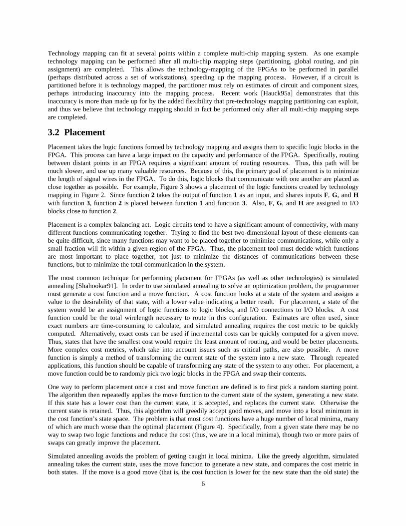
3.2 Placement
Placement takes the logic functions formed by technology mapping and assigns them to specific logic blocks in theFPGA. This process can have a large impact on the capacity and performance of the FPGA. Specifically, routingbetween distant points in an FPGA requires a significant amount of routing resources. Thus, this path will bemuch slower, and use up many valuable resources. Because of this, the primary goal of placement is to minimizethe length of signal wires in the FPGA. To do this, logic blocks that communicate with one another are placed asclose together as possible. For example, Figure 3 shows a placement of the logic functions created by technologymapping in Figure 2. Since function 2 takes the output of function 1 as an input, and shares inputs F, G, and Hwith function 3, function 2 is placed between function 1 and function 3. Also, F, G, and H are assigned to I/Oblocks close to function 2.
Placement is a complex balancing act. Logic circuits tend to have a significant amount of connectivity, with manydifferent functions communicating together. Trying to find the best two-dimensional layout of these elements canbe quite difficult, since many functions may want to be placed together to minimize communications, while only asmall fraction will fit within a given region of the FPGA. Thus, the placement tool must decide which functionsare most important to place together, not just to minimize the distances of communications between thesefunctions, but to minimize the total communication in the system.
The most common technique for performing placement for FPGAs (as well as other technologies) is simulatedannealing [Shahookar91]. In order to use simulated annealing to solve an optimization problem, the programmermust generate a cost function and a move function. A cost function looks at a state of the system and assigns avalue to the desirability of that state, with a lower value indicating a better result. For placement, a state of thesystem would be an assignment of logic functions to logic blocks, and I/O connections to I/O blocks. A costfunction could be the total wirelength necessary to route in this configuration. Estimates are often used, sinceexact numbers are time-consuming to calculate, and simulated annealing requires the cost metric to be quicklycomputed. Alternatively, exact costs can be used if incremental costs can be quickly computed for a given move.Thus, states that have the smallest cost would require the least amount of routing, and would be better placements.More complex cost metrics, which take into account issues such as critical paths, are also possible. A movefunction is simply a method of transforming the current state of the system into a new state. Through repeatedapplications, this function should be capable of transforming any state of the system to any other. For placement, amove function could be to randomly pick two logic blocks in the FPGA and swap their contents.
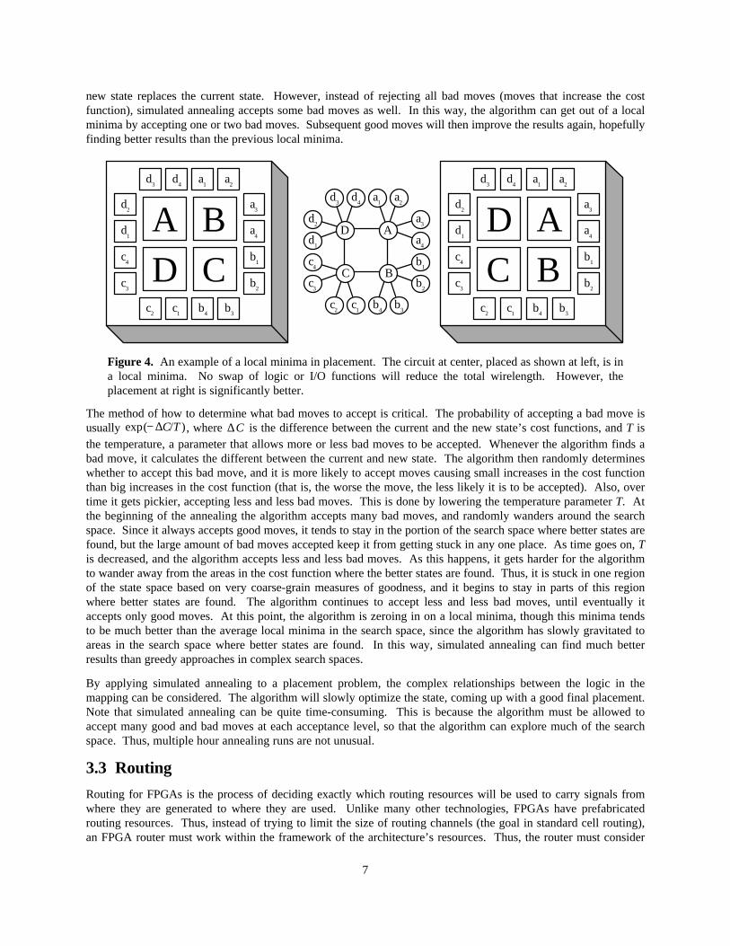
One way to perform placement once a cost and move function are defined is to first pick a random starting point.The algorithm then repeatedly applies the move function to the current state of the system, generating a new state.If this state has a lower cost than the current state, it is accepted, and replaces the current state. Otherwise thecurrent state is retained. Thus, this algorithm will greedily accept good moves, and move into a local minimum inthe cost function’s state space. The problem is that most cost functions have a huge number of local minima, manyof which are much worse than the optimal placement (Figure 4). Specifically, from a given state there may be noway to swap two logic functions and reduce the cost (thus, we are in a local minima), though two or more pairs ofswaps can greatly improve the placement.
Simulated annealing avoids the problem of getting caught in local minima. Like the greedy algorithm, simulatedannealing takes the current state, uses the move function to generate a new state, and compares the cost metric inboth states. If the move is a good move (that is, the cost function is lower for the new state than the old state) the
7
new state replaces the current state. However, instead of rejecting all bad moves (moves that increase the costfunction), simulated annealing accepts some bad moves as well. In this way, the algorithm can get out of a localminima by accepting one or two bad moves. Subsequent good moves will then improve the results again, hopefullyfinding better results than the previous local minima.
D A
BC
d4
d2
d1
c4
c3
c2
c1
b4
b3
b2
b1
a4
a3
a2
a1
d3
A BD C
d2
d1
c4
c3
c2
c1
b4
b3
d3
d4
a1
a2
a3
a4
b1
b2
D AC B
d2
d1
c4
c3
c2
c1
b4
b3
d3
d4
a1
a2
a3
a4
b1
b2
Figure 4. An example of a local minima in placement. The circuit at center, placed as shown at left, is ina local minima. No swap of logic or I/O functions will reduce the total wirelength. However, theplacement at right is significantly better.
The method of how to determine what bad moves to accept is critical. The probability of accepting a bad move isusually exp(− ∆C/T ), where ∆C is the difference between the current and the new state’s cost functions, and T isthe temperature, a parameter that allows more or less bad moves to be accepted. Whenever the algorithm finds abad move, it calculates the different between the current and new state. The algorithm then randomly determineswhether to accept this bad move, and it is more likely to accept moves causing small increases in the cost functionthan big increases in the cost function (that is, the worse the move, the less likely it is to be accepted). Also, overtime it gets pickier, accepting less and less bad moves. This is done by lowering the temperature parameter T. Atthe beginning of the annealing the algorithm accepts many bad moves, and randomly wanders around the searchspace. Since it always accepts good moves, it tends to stay in the portion of the search space where better states arefound, but the large amount of bad moves accepted keep it from getting stuck in any one place. As time goes on, Tis decreased, and the algorithm accepts less and less bad moves. As this happens, it gets harder for the algorithmto wander away from the areas in the cost function where the better states are found. Thus, it is stuck in one regionof the state space based on very coarse-grain measures of goodness, and it begins to stay in parts of this regionwhere better states are found. The algorithm continues to accept less and less bad moves, until eventually itaccepts only good moves. At this point, the algorithm is zeroing in on a local minima, though this minima tendsto be much better than the average local minima in the search space, since the algorithm has slowly gravitated toareas in the search space where better states are found. In this way, simulated annealing can find much betterresults than greedy approaches in complex search spaces.
By applying simulated annealing to a placement problem, the complex relationships between the logic in themapping can be considered. The algorithm will slowly optimize the state, coming up with a good final placement.Note that simulated annealing can be quite time-consuming. This is because the algorithm must be allowed toaccept many good and bad moves at each acceptance level, so that the algorithm can explore much of the searchspace. Thus, multiple hour annealing runs are not unusual.
3.3 Routing
Routing for FPGAs is the process of deciding exactly which routing resources will be used to carry signals fromwhere they are generated to where they are used. Unlike many other technologies, FPGAs have prefabricatedrouting resources. Thus, instead of trying to limit the size of routing channels (the goal in standard cell routing),an FPGA router must work within the framework of the architecture’s resources. Thus, the router must consider
8
the congestion of signals in a channel, making sure than no more routes are made through a region than there areresources to support them. Otherwise, if too many resources are required the routing fails, while in othertechnologies the region could just be enlarged.
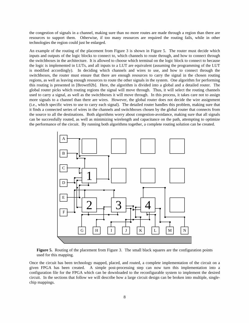
An example of the routing of the placement from Figure 3 is shown in Figure 5. The router must decide whichinputs and outputs of the logic blocks to connect to, which channels to route through, and how to connect throughthe switchboxes in the architecture. It is allowed to choose which terminal on the logic block to connect to becausethe logic is implemented in LUTs, and all inputs to a LUT are equivalent (assuming the programming of the LUTis modified accordingly). In deciding which channels and wires to use, and how to connect through theswitchboxes, the router must ensure that there are enough resources to carry the signal in the chosen routingregions, as well as leaving enough resources to route the other signals in the system. One algorithm for performingthis routing is presented in [Brown92b]. Here, the algorithm is divided into a global and a detailed router. Theglobal router picks which routing regions the signal will move through. Thus, it will select the routing channelsused to carry a signal, as well as the switchboxes it will move through. In this process, it takes care not to assignmore signals to a channel than there are wires. However, the global router does not decide the wire assignment(i.e., which specific wires to use to carry each signal). The detailed router handles this problem, making sure thatit finds a connected series of wires in the channels and switchboxes chosen by the global router that connects fromthe source to all the destinations. Both algorithms worry about congestion-avoidance, making sure that all signalscan be successfully routed, as well as minimizing wirelength and capacitance on the path, attempting to optimizethe performance of the circuit. By running both algorithms together, a complete routing solution can be created.
1
2 3 4
A
B
C
D
E
F
G H I J K L M N
Figure 5. Routing of the placement from Figure 3. The small black squares are the configuration pointsused for this mapping.
Once the circuit has been technology mapped, placed, and routed, a complete implementation of the circuit on agiven FPGA has been created. A simple post-processing step can now turn this implementation into aconfiguration file for the FPGA which can be downloaded to the reconfigurable system to implement the desiredcircuit. In the sections that follow we will describe how a large circuit design can be broken into multiple, single-chip mappings.
9
4.0 Multi-Chip Systems
FPGA vendors have provided tools that can take a mapping intended for a single FPGA, and automatically create aconfiguration file, and thus an FPGA-based realization of the design. However, many FPGA-based systems do notconsist of simply a single FPGA, but may have multiple FPGAs connected together into a multi-FPGA system, aswell as perhaps memory devices and other fixed resources. Mapping a circuit to such a system is much morecomplex than the single-chip mapping process, including considerations and constraints not found within a singleFPGA. In this section we discuss techniques for solving these problems, presenting the current state-of-the-art inmulti-FPGA mapping. These techniques, in conjunction with those described in the previous section, are capableof taking a complex circuit (one that is much larger than the capacity of a single FPGA) and create a completeimplementation.
4.1 Software Assist for the Hand-Mapping Process
Perhaps the simplest method for mapping to a multi-FPGA system (at least from the tool developer’s standpoint) isto have the user produce the mapping from scratch, specifying the complete implementation details. This requiresthe user to have a good understanding of their application and the reconfigurable system, but will potentially allowthe user to create a much better implementation than is possible with an automatic mapping system.
Producing a mapping completely from scratch, with no software support, is often impossible. At a minimum, formost FPGAs it is necessary to rely on a software tool to create the bit patterns to load into the FPGA from a placedand routed circuit, since the information to do this by hand is often not provided by the FPGA vendors. However,there are several other ways in which software automation can help in even a hand-mapping environment. Forexample, when laying out a regular structure like an adder circuit, a user need not specify the exact location ofeach individual adder cell, and would much rather just state that the adder cells are placed next to one-anotherdown a specific column in the FPGA. Also, a user may wish to create a specific hardware template for acommonly occurring component in their design and then replicate it as needed. Several such systems, which act asassistants to the hand-mapping process, and automate some of the less critical portions of the mapping process,have been produced [Gokhale95, Vuillemin96]. These systems remove some of the complexity of the hand-mapping process, allowing the designer to concentrate on the more important aspects of the design. However,these systems do not replace the designer, and require a user with a high degree of knowledge and sophistication.For less experienced users, or less demanding tasks, higher levels of automation are often essential.
In the rest of the paper we concentrate on the automation of the mapping process, attempting to develop a“compiler” for an FPGA-based system. However, with each of these systems it is important to realize that hand-mapping is often an alternative, and the quality losses due to software automation must be balanced against thedesign complexity of performing that optimization by hand. It is important to note that most high-performancesystems based on FPGAs have largely been mapped to manually. Hopefully, in the decade to come we willtransition to a model more in line with general-purpose computing, where most programs are translated from ahigh-level language into machine instructions via a completely automatic mapping process, though where there isstill the potential for assembly-language programming (the hand-mapping of the software world) in situationswhere the performance gains are large enough or important enough to make such efforts worthwhile.
4.2 Partitioning and Global Placement
The user of a multi-FPGA system usually specifies the desired functionality as a single, large structural circuit.This circuit is almost always too large to fit into a single FPGA, and must instead be split into pieces small enoughto fit into multiple FPGAs. When the design is split up, there will be some signals that need to be communicatedbetween FPGAs because two or more logic elements connected to this signal reside on different FPGAs. Thiscommunication is a problem for a multi-FPGA system, because the amount of I/O resources on the FPGAs tends tobe used up long before the logic resources are filled.
Because I/O resources are the main limitation on logic capacity in a multi-FPGA system, the primary goal of thepartitioner, the tool that splits logic up into FPGA-sized partitions, is to minimize the communication betweenpartitions. There have been many partitioning algorithms developed that have as a primary goal the reduction of

10
inter-partition communication, and which can split a design into multiple pieces, including algorithms designedspecifically to map into multiple FPGAs [Kuznar93, Woo93, Kuznar94, Weinmann94, Chan95, Huang95b,Kuznar95, Fang96]. One such algorithm [Chou94] is also designed to efficiently handle the large circuitsencountered during logic emulation. Instead of partitioning the entire circuit, it instead focuses only on a smallportion of the circuit at a time. Although this speeds up the partitioning, it may cause the algorithm to ignore moreglobal concerns, including assigning logic to more than one partition. To fix these problems, the algorithm uses antechnique inspired by the ESPRESSO II logic minimization package [Brayton85] to recombine and restructure thepartitioning. If logic is assigned to multiple partitions, the algorithm will restructure the partitions to remove theoverlap. Also, more global concerns will be handled by breaking the partitions initially created into smallerportions and recombining them into (hopefully) a better final partitioning.
Unfortunately, many previous multiple-FPGA algorithms are not designed to work inside a fixed topology.Specifically, most multi-way partitioning algorithms, algorithms that break a mapping into more than 2 parts,assume that there is no restriction on which partitions communicate. They only seek to minimize the total amountof that communication, measured as either the total number of nets connecting logic in two or more partitions (thenet-cut metric), or the total number of partitions touched by each of these cut nets (the pin-cut metric). These arereasonable goals for when the partitioner is run before the chips are interconnected, and is used in cases wheresomeone is building a custom multi-FPGA system for a specific application. However, most multi-FPGA systemsare prefabricated, with the FPGAs connected in a routing topology designed for general classes of circuits, andthese connections cannot be changed. Thus, some FPGAs may be interconnected in the topology, while others willnot, and the partitioner needs to understand that the cost of sending a signal between pairs of FPGAs depends onwhich FPGAs are communicating. Even when the multi-FPGA system is custom designed for an application, latermodifications to the circuit will require similar, topology-aware partitioning tools.
3 41 2
Figure 6. Example system for topological effects on multi-FPGA system partitioning.
For an example of topological issues in multi-FPGA system partitioning, consider a linear array of 4 FPGAs,numbered 1-4 (Figure 6). A signal communicated between FPGAs 1 & 2 will consume two I/Os, one on eachFPGA, since the FPGAs are directly connected. A signal between FPGAs 1 & 4 will consume six I/Os, twobetween 1 & 2, two between 2 & 3, and two between 3 & 4. Thus, when partitioning onto this linear array ofFPGAs, it is better to have two signals being communicated, one between 1 & 2, and one between 2 & 3, than it isto have a single signal communicated between 1 & 4. In order to do a reasonable job of partitioning onto a multi-FPGA system, the partitioner needs to be aware of the topology onto which it is partitioning. For this reason thestep of global placement, the assigning of partitions to specific FPGAs in the system, is often done simultaneouslywith partitioning. Otherwise it is hard for a partitioner to understand the cost of communication within a giventopology if it does not know where the partitions it is creating lie within this topology.
One method for performing partitioning onto a multi-FPGA systems is to handle it as a placement problem.Specifically, we can apply simulated annealing to the partitioning problem, allowing the tool to assign logic tospecific FPGAs in a multi-FPGA system [Roy94, Roy-Neogi95]. Just as in placement for single FPGAs, the toolrandomly assigns logic to functional units, which in this case are the logic-bearing FPGAs. The logic assigned toan FPGA is restricted to the FPGA’s capacity. The partitioner then uses the simulated annealing algorithm to seekbetter placements through random moves under an annealing schedule. However, one problem with partitioningonto a multi-FPGA topology is that it can be difficult to estimate the routing costs of a given assignment. In anFPGA, routing distances tend to obey a simple geometric cost metric, with the physical distance between sourceand sink directly relating to the routing costs. In a multi-FPGA system, there may be an arbitrary connectionpattern between FPGAs, with no simple geometric cost metric accurately capturing the actual routing complexity.However, in meshes and other regular architectures, geometric routing cost metrics can be developed, andsimulated annealing or other algorithms can be applied. Another possibility for such a system is the partitioner forthe Anyboard system [Thomae91, Van den Bout92, Van den Bout93], which applies a variant of the Kernighan-

11
Lin algorithm [Kernighan70] to a bus-structured multi-FPGA system where interconnect costs are easilydetermined.
In order to handle the partitioning problem on topologies that do not admit a simple routing cost metric, it isnecessary to come up with some other method of estimating routing complexity. One method is to model therouting problem as a multicommodity flow problem and use this as part of the partitioning process [Vijayan90].The multicommodity flow problem can estimate the routing complexity on a general graph, meaning that thisapproach can be used on an arbitrary multi-FPGA topology. However, the flow calculation can be very complex,and thus cannot be used in the inner loop of a complex partitioning algorithm. Thus, the flow calculation is onlyrun after a significant number of iterations of a normal algorithm, which uses the previous flow calculation as anestimate of current routing conditions. However, even with this modification, their algorithm has an exponentialworst-case complexity.
Although the approaches discussed previously can develop reasonably accurate estimates of partitioning quality,they take a significant amount of runtime to complete. The approach in [Vijayan90] has an exponential worst-casecomplexity, and simulated annealing is notoriously slow. An alternative to both of these algorithms is to adapt thestandard partitioning algorithms [Alpert95], which ignore interconnection limitations, to partitioning onto atopology. For crossbar topologies, multi-way partitioning algorithms can be directly applied. In a crossbartopology [Hauck98] routing costs are adequately captured by the amount of inter-FPGA signals connected to eachlogic-bearing FPGA in the system, which is the optimization metric of many multi-way partitioning algorithms.For a hierarchical crossbar (which has multiple standard crossbar topologies connected together by higher levels ofcrossbar interconnections) multi-way partitioning algorithms can be recursively applied. In a hierarchical crossbarthere are N subsets of the topology interconnected in the highest level in the crossbar. Minimizing thecommunication between these N subsets is the primary concern in a hierarchical crossbar, because the connectionsat the highest level of a hierarchical crossbar tend to be the primary routing bottleneck. Thus, a multi-waypartitioning algorithm can split the circuit into N pieces, one per subset of the topology, and optimize for thisbottleneck. At this point each of these subsets can be handled independently, either as a crossbar or a smallerhierarchical crossbar. In this way, standard multi-way partitioning algorithms can be recursively applied to ahierarchical crossbar, yielding a fairly fast partitioning algorithm.
B C
DA
F E
H I
JG
L K
N O
PM
R Q
23
1
56
4
89
7
B C
DA
F E
H I
JG
L KN O
PM
R Q
2
31 5
64 8
971
2
3
Figure 7. An example of the suboptimality of recursive bipartitioning. We are partitioning to the multi-FPGA system at middle, and the best first cut is shown at left (gray line). The next partitioning wouldhave to cut nine signals. We can instead partition as shown at right, cutting a total of two signals.
A similar recursive partitioning approach can be applied to other multi-FPGA system topologies. A split in themulti-FPGA topology is chosen that breaks the system into two or more subsets, and the logic is split into a similarnumber of pieces. These subsets are then subdivided repeatedly until the mapping has been broken into N pieces,one per FPGA in the system. By using a fast bipartitioning or multi-way partitioning algorithm, a complete

12
partitioning of the circuit onto the multi-FPGA topology can be performed. Such an approach has been used toquickly partition circuits onto the Teramac system [Snider95].
There are two problems with recursive bipartitioning onto a multi-FPGA system: it is greedy (overlooking moreglobal concerns), and it ignores the multi-FPGA topology. It is greedy because the first bipartitioning attempts tofind the best possible bipartitioning. While it may find a good way to split a mapping if it is only going to bebroken into two parts, it may be a poor choice as a starting point for further cuts. The first split may require only asmall amount of communication between the two halves of the system, but later cuts may require much morecommunication. We may have been better served having a somewhat larger initial cut, which might easecongestion on later cuts, and thus minimize the overall amount of inter-partition communication. An example ofthis is shown in Figure 7.
CBA
GFE
D
H1
CBA
GFE
D
H
CBA
GFE
D
H1
2CBA
GFE
D
H1
2
3 3
A B C D
E F G H
Circuit ABEF CDGH
EF GH
AB CD
Figure 8. Example of iterative bipartitioning. The circuit (top left) is partitioned onto the multi-FPGAtopology (bottom left) in a series of steps. Each partitioning corresponds to the most critical bottleneckremaining in the multi-FPGA system, and after each partitioning the placement of the logic is restricted toa subset of the topology (labeling on circuit partitions).
The greediness of iterative bipartitioning can be taken advantage of in order to map onto a specific multi-FPGAtopology [Hauck95b]. Specifically, the multi-FPGA topology itself will have some bottleneck in its topology, someplace where the expected communication is much greater than the routing resources in the multi-FPGA topology.For example, going back to the linear array of FPGAs discussed earlier (Figure 6), it is clear that if the number ofwires connecting adjacent FPGAs is the same throughout the system, then the wires between the middle FPGAs,numbers 2 & 3, will be the most heavily used, since with an equal number of FPGAs on either side of this pair ofFPGAs the communication demand should be the highest. Not all multi-FPGA systems will be linear arrays ofFPGAs, but within most of them will be some set of links that are the critical bottleneck in the system. If weiteratively partition the circuit being mapped onto a topology such that the first cut in the circuit falls across thiscritical bottleneck, with the logic in one partition placed on one side of the bottleneck, and the other partition onthe other side of the bottleneck, then this greedy early cut is performed exactly where the best cut is necessary. Wecan continue this process, performing partitionings corresponding to the remaining bottlenecks in the system. Inthis way we take advantage of the greedy nature of iterative bipartitioning, performing the early, greedy cuts wherenecessary to relieve the most significant bottlenecks in the topology, while later cuts (which are hurt by thegreediness of earlier cuts) are performed where lower quality cuts can be tolerated, since they correspond tolocations that are not critical bottlenecks in the system. An example of this process is shown in Figure 8. Whilethis does not totally avoid the suboptimality of iterative bipartitioning, it does help limit it.
There are other ways of improving on the basic hierarchical greedy scheme. In [Kim96], Kim and Shin presentalgorithms in which a first cut hierarchical partitioning phase is followed by a second pass iterative optimizationphase in which all constraints are satisfied. Chou et al. [Chou94] present a scheme that uses a local ratio-cutclustering followed by a set covering partitioning method. [Kuznar94] uses functional replication to improve thequality of partitioning.
13
4.2.1 Partitioning for VirtualWires
The gate versus IO requirements for partitioned blocks are often mismatched with the gate versus IO balance incommercial FPGAs. Generally, experience has shown that for a given number of gates, partitioned blocks tend tohave more IOs than FPGAs do. A compilation technique called VirtualWires [Babb93] attempts to bridge this gapthrough a multiplexing and pipelining approach that enables superfluous gates on FPGAs to be traded for pins,thus allowing more efficient use of FPGA resources. The basic idea is that when the number of logical signals thatmust cross partitioned boundaries is greater than the number of physical pins on an FPGA, the VirtualWirestechnique multiplexes and pipelines several logical signals on each physical FPGA pin. Consequently, themultiplexors allow more logical signals to cross FPGA boundaries, but incur a gate cost that is proportional to thenumber of logical signals and largely independent of the number of physical pins. Multiplexing and pipelining ofmultiple logical signals onto a single physical pin is orchestrated against a discrete time-base provided by a newclock called the virtual clock. A VirtualWires compiler schedules both logic evaluation and communication onspecific cycles of the virtual clock. Scheduling is discussed further in Section 4.3.3.
Partitioning algorithms for VirtualWires are modified forms of those used in traditional systems, differing largelyin the cost constraints or the optimization criteria they use during the optimization process [Agarwal95]. Let usrepresent partitioning constraints as follows. Suppose Gi is the number of gates in partition i, and Pi is the numberof pins in partition i. Also suppose that Gmax and Pmax are the maximum number of gates and pins (respectively)that an FPGA can support.
In a traditional system, the constraints faced by the partitioner are: Gi � Gmax and Pi � Pmax. The constraints aregraphically represented in the left hand side of Figure 9 showing the feasible partitioning region in terms of gatesand pins. Partitioning attempts to divide a set of gates into the minimum number of partitions that satisfy theabove constraints. Typically, the traditional process involves dividing the number of gates into some number ofpartitions in a manner that satisfies the gate constraint, and then moving gates between partitions to minimize thenumber of pins in an attempt to satisfy pin constraints.
Now, let us consider the VirtualWires case. Let c denote the “cost” in terms of logic gates of a virtual wire. Inother words, let c represent the average number of overhead logic gates in a VirtualWires system that are requiredto implement a single logic signal that must be sent or received by an FPGA (for simplicity, we assume that bothinputs and outputs cost the same). In our experience c is roughly four gates. In a VirtualWires system, theconstraint faced by the partitioner is Gi + c Pi � Gmax. The resulting constraint space for the VirtualWires case isdenoted in Figure 10. As can be seen, because pin constraints can be folded into a gate constraint, the feasiblespace is larger with VirtualWires. The intuition why the feasible space is larger is that gates can be traded forpins. If a given partition has more pins than the others, then the increased number of pins can be compensated forby placing fewer gates on that FPGA.
As before, partitioning attempts to divide a set of gates into the minimum number of partitions that satisfy theabove constraint. VirtualWires partitioning involves dividing the number of gates into some number of partitionsand then moving gates between partitions to reduce the number of IO so that the above gate constraint is satisfiedfor each partition. The partitioning algorithm itself can be one of those described earlier.
4.2.2 Global Placement
The placement of partitions on FPGAs can be accomplished as a separate, standalone phase in the compilationprocess, or it can be combined with partitioning. A separate placement phase simplifies the software system, butthe overall results are generally poorer. The placement process assigns partitions to FPGAs. Placement attemptsto put partitions that communicate intensely or partitions that are in timing critical paths as close together aspossible. Because the placer must attempt to optimize several criteria, such as global communication volume andthe critical path length, simulated annealing is a commonly used technique.

14
Gi Gmax<
200 400 600 800 1000
800
1600
2400
3200
4000
Pins
Pi Pmax<
Gat
es
Figure 9. Constraints used by a traditional partitioner.
200 400 600 800 1000
800
1600
2400
3200
4000
Pins
Gmax<Gi + c Pi
Gat
es
Figure 10. Constraints used by a VirtualWires partitioner.
To apply simulated annealing to the multi-FPGA placement problem requires both a cost function and a move function. The move function for a multi-FPGA system usually involves simply swapping the contents of two FPGAs. Developing a cost function for this problem is more difficult, since considerations such as critical path length and routing congestion must often be considered.
An important factor in such algorithms is that the move generator be able to estimate the move cost quickly - a move function that requires recalculating the routing of the entire system after each move is impractical. Unfortunately, to compute the true routing complexity or critical path length for a given configuration of the system requires just such an action - the swap of two partitions between FPGAs can significantly change most routing-related costs. Estimates can be made by ignoring congestion, and assuming all routes can take the minimum path between FPGAs. However, if there is routing congestion due to a given placement of the logic, this routing estimator will ignore this effect, and yield an overly optimistic cost metric. Thus, the simplicity of separating the partitioning and global routing steps must be balanced against the potential for lower-quality results due to inaccurate cost metrics.

15
4.3 Global Routing
Global routing is the process of determining through which FPGAs or interconnection switches to route inter-FPGA signals. Note that the related problem of determining which specific pins to use to carry a signal is oftenhandled separately; it will be discussed later in this paper. In cases where a signal needs to connect between onlytwo directly connected FPGAs, this step is usually simple. No intermediate FPGA is needed to carry this signal,and the routing can be direct. However, in some cases the wires that directly connect these FPGAs may be used upby other signals. The signal will need to take alternate routes, routes that may lead through other FPGAs. Forlong-distance routing, there may be many choices of FPGAs to route through. A global router attempts to chooseroutes in order to make the most direct connections, thus minimizing delay and resource usage, while making surethat there are sufficient routing resources to handle all signals.
Routing is a problem in numerous domains, including standard cells, gate arrays, circuit board layout, and singleFPGAs. Global routing for multi-FPGA systems is similar to routing for single FPGAs. Specifically, in an FPGAthe connections are fixed and finite, so that the router cannot add resources to links that are saturated, and theconnections may not obey strict geometrical distance metrics. The same is true for a multi-FPGA system. In thecases of standard cells and gate arrays, the size of routing channels can (usually) be increased, and in circuit boardrouting extra layers can be added. Thus, for multi-FPGA global routing many of the techniques from single-FPGArouting are also applicable.
In the sections that follow we will discuss routing algorithms for several different types of systems, includingcrossbar and direct-connect systems. We will also consider global routing for Virtual Wires systems.
DCBA
ZYXW
Figure 11. Crossbar routing topology. The chips at top are used purely for routing, while the FPGAs atbottom handle all the logic in the system.
4.3.1 Global Routing for Crossbar Topologies
In a crossbar topology (Figure 11), a signal that needs to be routed between FPGAs will always start and end atlogic-bearing FPGAs, since routing-only chips have no logic in them. Thus, routing any signal in the system,regardless of how many FPGAs it needs to connect to, requires routing through exactly one other chip, and thatchip can be any of the routing-only chips. This is because each routing-only chip connects to every logic-bearingFPGA, and the routing-only chips have exactly the same connectivity. Thus, routing for a crossbar topologyconsists simply of selecting which routing-only chip an inter-FPGA signal should route through, and a routingalgorithm seeks only to route the most number of signals. Note that this does require some effort, since someassignments of signals to routing-only chips allow much less communication than others. For example, assumethat each of the connections between chips in Figure 11 consist of 3 wires, and assume that we are attempting toroute three-terminal wires, with connections evenly distributed between the logic-bearing FPGAs. If we routesignals between FPGAs ABC through W, ABD through X, ACD through Y, and BCD through Z, we will be ableto route three signals through each routing-only chip, for a total of 12 signals. At this point, no further routing can
16
be performed, even of two-terminal wires. We can instead route one ABC, one ABD, one ACD, and one BCDwire through each of the routing-only chips, achieving a total of 16 routed signals.
There have been several algorithms proposed for the routing of signals in crossbar topologies. [Mak95b] presentsan algorithm that is optimal for 2-terminal routing, as well as proof that routing for multi-terminal nets is NP-Complete. The routing algorithm is based on the idea that if too many routes are assigned to a given routing-onlychip, there must be some routing-only chip that is underutilized. Otherwise, there would be no possible routing forthis mapping. Given this fact, the routes going through these two chips can be balanced, so that there is almost anidentical number of nets going to each of these routing-only chip from each logic-bearing chip. Thus, to performthe routing for a crossbar topology, simply assign all of the nets to a single routing-only chip, and then iterativelybalance the demand on routing-only chips until the routing is feasible. Since the problem of routing multi-terminalnets in a crossbar topology is NP-Complete, heuristic algorithms have been proposed [Butts91, Kadi94]. Thesegreedily route signals through routing-only chips based on their current utilization. Because of this, they may notalways find a routing solution in situations where such a solution exists, even in the case of purely 2-terminalrouting. Thus, there may be some benefit in combining a heuristic approach to multi-terminal net routing with theoptimal approach to 2-terminal net routing, though it is not clear how this could be done. An alternative is tobreak all multi-terminal nets into a spanning tree of only two-terminal nets. Then, the optimal algorithm can beapplied to routing these 2-terminal nets. [Mak95a] proposes an algorithm which will perform such adecomposition, as well as make sure that the I/O capacity of the FPGAs are not violated by the splitting of multi-terminal nets. However, this decomposition requires extra I/O resources on some FPGAs in the system toaccomplish this splitting, and if such resources are not available, this algorithm cannot find a routing, even thoughsuch a routing may in fact exist for non-decomposed multi-terminal nets.
4.3.2 Global Routing in Direct-Interconnect Systems
Thus far we have looked at routing for indirect interconnects. Indirect interconnection systems are those in whichlogic bearing FPGAs are distinct from FPGAs or switches that handle routing tasks. Routing with directinterconnects is a little more complicated. In a direct interconnect hardwire system, routing is the problem ofselecting the set of FPGAs through which to route a signal between a pair of partitions. The following algorithmdescribes a routing approach for direct interconnect hardwire systems. We first present a simple approach andthen suggest methods to improve the route quality.
This routing method begins by constructing the FPGA channel graph. This is a directed graph that represents theFPGA topology in which each node represents an FPGA and each directed edge represents a channel. A channel isthe set of directed connections from one FPGA to another. Each channel has a width representing the number ofphysical wires in the channel. The use of directed channels with predetermined widths is a simplification becausethe IO pins in typical FPGAs can be configured to behave as either outputs or inputs. Figure 12 shows an exampleinput circuit that we wish to map onto a mesh connected FPGA topology. The channel graph for the FPGAtopology is shown in Figure 13. The latter figure also shows the initial values of the available channel capacities.

17
FPGA F0
FPGA F1
FPGA F3
FPGA F2
D Q
D Q
a
bc
Figure 12. Input circuit (left) and FPGA topology (right).
F0
2F
1
1
F3
2F
2
1
1 12 2
Figure 13. FPGA channel graph showing the initial values of the available channel capacities.
The algorithm also relies on a distance weight and the available channel capacity of each channel in the channelgraph. For channel C, let Cd represent the distance weight, let Cw represent the physical channel width, and let Ca
represent the available channel capacity. Distance weights are used to turn off channels that are full. Assign adefault distance weight of 1 to each channel and initialize the available channel capacity to the channel width. Inother words, initialize,
Cd = 1
Ca = Cw
The algorithm works by repeated applications of the following step: pick a wire and find a route comprising asequence of channels from its source partition to its destination partition. If a net has d > 1 destination terminals,then the router can treat the net as d two-terminal wires, each of which connects the source terminal to one of thedestination terminals.
More specifically, the algorithm applies the following step until all nets have been assigned a route.
1. Pick a wire and find the partition that sources the net. Let s denote the source partition and let sf denote theFPGA on which the source partition is placed. Similarly, let d be the destination partition for the net and let df
be the FPGA on which the destination partition lies.
2. Find the shortest path Psd (using a standard shortest path algorithm, where id

Cia = 0 , for any i = 0 … n-1, then set Ci
d = ∞ .
4. Associate the path Psd with the wire and mark the wire so it is not picked again.
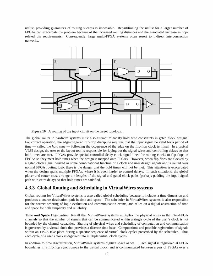
As an example, suppose the design in Figure 12 is partitioned and placed as in Figure 14. Also suppose that thewire a is the first wire picked to be routed. The source FPGA sf for this wire is F1 and the destination FPGA df isF3. The initial state of the channel graph is as shown in Figure 13. The state of the graph after wire a is routed isshown in Figure 15. Figure 16 shows a possible routing of all the nets.
F3
F2
F0
F1
D Q
a
b c
D Q
Figure 14. A partition and placement of the input circuit.
F0
2F
1
1
F3
1F
2
1
1 02 2
Figure 15. Channel graph showing available channel capacities after routing the net a.
The above algorithm can be optimized in many ways. For example, consider this optimization for multi-terminalwires n that are represented as d two-terminal wires n1, n2, n3, … nd. Suppose that the two-terminal wires n1, n2, …ni-1 have been previously routed, and we are attempting to route wire ni. We can choose as the source FPGA for ni
any of the FPGAs that are connected by wires n1, n2, … ni-1, potentially saving valuable channel capacity.
In a direct-interconnect system, the channels can sometimes run out of capacity and the global router can fail tofind any path to route a given wire. The router can attempt to make further progress by ripping out one or morepreviously assigned routes to make space in the congested channel and unmarking the related wires. However,because pin usage for routing hops in a direct interconnect system is related to the characteristics of the input
19
netlist, providing guarantees of routing success is impossible. Repartitioning the netlist for a larger number ofFPGAs can exacerbate the problem because of the increased routing distances and the associated increase in hop-related pin requirements. Consequently, large multi-FPGA systems often resort to indirect interconnectionnetworks.
F3
F2
F0
F1
D Q
a
bc
D Q
Figure 16. A routing of the input circuit on the target topology.
The global router in hardwire systems must also attempt to satisfy hold time constraints in gated clock designs.For correct operation, the edge-triggered flip-flop discipline requires that the input signal be valid for a period oftime — called the hold time — following the occurrence of the edge on the flip-flop clock terminal. In a typicalVLSI design, the user or the layout tool is responsible for laying out the signal wires and controlling delays so thathold times are met. FPGAs provide special controlled delay clock signal lines for routing clocks to flip-flops inFPGAs so they meet hold times when the design is mapped onto FPGAs. However, when flip-flops are clocked bya gated clock signal derived as some combinational function of a clock and user design signals and is routed overnormal FPGA routing logic there is the danger that the hold times will not be met. This situation is exacerbatedwhen the design spans multiple FPGAs, where it is even harder to control delays. In such situations, the globalplacer and router must arrange the lengths of the signal and gated clock paths (perhaps padding the input signalpath with extra delay) so that hold times are satisfied.
4.3.3 Global Routing and Scheduling in VirtualWires systems
Global routing for VirtualWires systems is also called global scheduling because it includes a time dimension andproduces a source-destination path in time and space. The scheduler in VirtualWires systems is also responsiblefor the correct ordering of logic evaluation and communication events, and relies on a digital abstraction of timeand space for both simplicity and reliability.
Time and Space Digitization Recall that VirtualWires systems multiplex the physical wires in the inter-FPGAchannels so that the number of signals that can be communicated within a single cycle of the user’s clock is notbounded by the channel capacities. Sharing of physical wires and scheduling of computation and communicationis governed by a virtual clock that provides a discrete time-base. Computations and possible registration of signalswithin an FPGA take place during a specific sequence of virtual clock cycles prescribed by the scheduler. Thuseach cycle of a user's clock is digitized into multiple virtual clock cycles.
In addition to time discretization, VirtualWires systems digitize space as well. Each signal is registered at FPGAboundaries in a flip-flop synchronous to the virtual clock, and is communicated between a pair of FPGAs over a
20
physical wire on a given virtual clock cycle. Thus, all combinational timing paths are entirely within individualFPGAs. Timing paths also involve inter-FPGA crossings between directly connected FPGA pairs. Such a digitalspace abstraction not only provides a simple model to the scheduler, but yields system composability in which localtiming correctness guarantees global timing correctness.
Timing Resynthesis To facilitate complete event ordering control, all clocked elements in the system areresynthesized to use the virtual clock or signals synchronous to the virtual clock. As part of its routing process, thescheduler establishes the specific virtual cycle on which each storage element is enabled.
The TIERS Routing Approach The goal of the scheduler is to orchestrate all events in the system. In otherwords, it must prescribe the specific set of virtual clock cycles and the physical channels on which inter-FPGAsignals are communicated. Because a physical channel wire is allocated to a given signal only during a specifiedvirtual clock cycle, and not dedicated for all time, the scheduler must also determine the virtual cycle on which thegiven signal reaches its legal value and can be sampled for transmission outside the chip. The following is asimplified version of the TIERS algorithm for scheduling VirtualWires systems. For more details on TIERS(Topology Independent Pipelined Routing and Scheduling) see [Selvidge95].
The TIERS routing approach comprises the following steps:
1. Construct the FPGA channel graph.
2. Order inter-partition wires through a dependence analysis.
3. Determine the time-space path for each wire.
As with direct-interconnect systems, we first construct the FPGA channel graph. Each channel comprises a givennumber of wires. Although each wire is assumed to be able to carry a single signal during a given virtual clockcycle, each wire has an unbounded temporal extent. In other words, a given wire can transmit more signals byusing additional virtual cycles. Because channels can yield more capacity by using more virtual clock cycles, thesimplest VirtualWires scheduling algorithm does not require distance weights on the channels. Recall the distanceweights are used by hardwire routers to disconnect full channels.
FPGA F0 FPGA F1
FPGA F3 FPGA F2D Q
D Q
a
bc
d
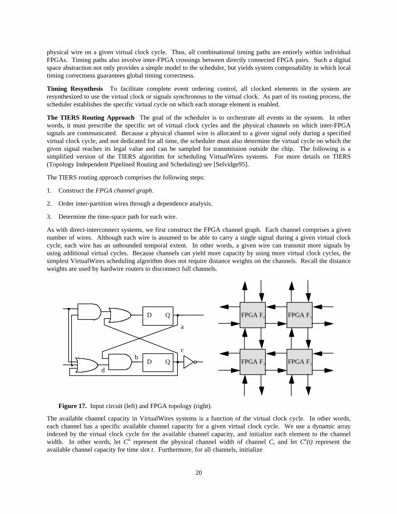
Figure 17. Input circuit (left) and FPGA topology (right).
The available channel capacity in VirtualWires systems is a function of the virtual clock cycle. In other words,each channel has a specific available channel capacity for a given virtual clock cycle. We use a dynamic arrayindexed by the virtual clock cycle for the available channel capacity, and initialize each element to the channelwidth. In other words, let Cw represent the physical channel width of channel C, and let Ca(t) represent theavailable channel capacity for time slot t. Furthermore, for all channels, initialize

21
C a(t) = Cw ∀t
Consider the same input circuit as before, but a FPGA topology with fewer physical connections as in Figure 17.The channel graph for this topology for use in VirtualWires routing is shown in Figure 18.
F0
[1,1,1...]F
1
[1,1,1...]
F3
[1,1,1...]F
2
[1,1,1...]
[1,1,1...][1,1,1...][1,1,1...]
[1,1,1...]
Figure 18 FPGA channel graph showing the initial values of the available channel capacities as afunction of the virtual cycle. Initially, C a(t) for each channel is 1 for all values of t.
User Clock Virtual Clock Wire d Wire a Wire b
Tr
Td
Ts
Tan
Tr
1 Td
Ts
Tan
Tr
1
d
a b
Figure 19. The relationship between the various scheduling times for signals a, d, and b. Wire b dependscombinationally upon a and d, and a is produced as the output of a flip flop.
The second step involves ordering inter-partition wires through a dependence analysis. In a discrete event system,the scheduler must guarantee that signals that are inputs to a combinational logic block must be available beforethe outputs of the combinational logic block can be routed. It does so by routing all input wires before routing anyof the output wires of any combinational block. System input wires and flip-flop output wires comprise the initialconditions for the recursive process implied by the above precedence constraint. A routing order consistent withthe above constraint is facilitated by creating a sorted list of inter-partition wires in which a wire wi precedesanother wire wj only if wi does not depend combinationally on wj. We also associate with each output wire of apartition the set of partition input wires on which it depends. As an example, wire a (shown in Figure 17) must bescheduled before wire b because b depends combinationally upon a.
The third step involves finding time-space routes for inter-partition wires. The routing algorithm does so byperforming the following sequence of operations to wires picked in order from the sorted list of wires, until allwires have been assigned a time-space route. A time-space route comprises a sequence of channel and virtual-cycle pairs from the source FPGA to the destination FPGA. As before, the router treats a net with d > 1 destinationterminals as d two-terminal wires, each of which connects the source terminal to one of the destination terminals.
1. Find the partition that sources the wire. Let s denote the source partition and let sf denote the FPGA onwhich the source partition is placed. Similarly, let d be the destination partition for the wire and let df bethe FPGA on which the destination partition lies.
2. Find the shortest path Psd (using a standard shortest path algorithm) between FPGAs sf and df. Psd issimply the sequence of channels Ci: i = 0 … n-1 in the shortest path between FPGAs sf and df.

22
The next set of steps determines the scheduling of the signals along the sequence of channels, and establishesthe ready time, arrival time, and send time for the signal (see Figure 19).
3. Determine the ready time Tr for the wire. The ready time of a wire is the earliest virtual cycle on whichthe wire attains its legal value. The ready times on system input wires and wires sourced by flip-flops isinitialized to 1. The ready times for other wires is one plus the maximum of the arrival times of the wireson which they depend. The one extra cycle allows for local combinational computation and registration ofthe signal in a flip-flop just prior to transmission through an FPGA output pin.
The arrival time Ta of a wire at an FPGA is the time (or virtual cycle) at which the signal on the wire willarrive at that FPGA. Assuming there are no combinational cycles in the circuit, picking wires accordingto the order in the sorted wire list guarantees their ready time can be calculated.
4. Compute the departure delay Td for the wire. The departure delay is the number of cycles the wire isdelayed at the FPGA as it waits for the availability of a sequence of available time slots along the path Psd.
One variant of the routing algorithm [Selvidge95] adds delays to a wire only at the source FPGA. That is,once a signal is scheduled for routing it suffers no additional delays till it reaches its destination FPGA.With the source-delay algorithm, a workable route can be obtained by looking for available channelcapacity in each of the channels in Psd during successive time slots starting with the ready time Tr of thewire (i.e., for Td = 0). If the signal is not routable starting at Tr, then the departure delay is increased untila workable route is found.
More formally, a wire is routable with departure delay Td if the following is true:
Cia(Tr + Td + i ) ≥ 0 , i = 0Kn − 1
The above assumes the each hop is accomplished in one virtual cycle.
5. Compute the send time Ts for the wire. The send time for a wire is the sum of the ready time and thedeparture delay for the net.
Ts = Tr + Td
6. Compute the arrival time of the net at the destination FPGA. Because our routing model assumes thatdelays are added only at the source, the arrival time is simply the sum of the send time and the number ofhops n. In other words, if the number of channels in Psd is n,
Ta = Ts + n
7. Decrement the available channel capacity for each channel in Psd for the time slot on which it is used bythe net.
Cia(Ts + i) = Ci
a (Ts + i) − 1 , i = 0Kn − 1
When the available channel capacity of any channel i during a time slot t is exhausted, i.e., Cia(t) = 0 Ca(t)
= 0, that channel will not be selected for further routing during time slot t.
8. Associate the path Psd, the send time Ts, and the arrival time Ta with the net. The Ts time is needed by afuture VirtualWires synthesis step that actually implements FPGA-specific state machines and enablesappropriate flip-flops and multiplexing logic on the appropriate virtual cycle. Ta, on the other hand, isneeded to compute the ready time of other nets that depend on it.
As an example, consider wires a, b, and c shown in Figure 17. One possible ordering of the wires in the dependsorted wire list is a, c, b. Tr for both a and c is 1 because both are sourced by a flip flop in the original design.Since both can be scheduled for transmission immediately Td for both is 0, and therefore Ts for both is 1 Asdepicted in Figure 21, the wire a can be scheduled on the channel from F1 to F2 on virtual cycle 1 and on the

23
channel from F2 to F3 on the following virtual cycle. Thus, Ta for a is 3 since n (the number of hops) is 2. Thechannel graph following the scheduling of a is as shown in Figure 20. Similarly, wire c can be scheduled on thechannel from F2 to F3 on virtual cycle 1. Tr for wire b can be calculated as 3 (one plus the arrival time for a).Because the channel from F3 to F2 is available, Td for b is 0, and b can be scheduled on virtual cycle 3.
F0
[1,1,1...]F
1
[1,1,1...]
F3
[1,0,1...]F
2
[1,1,1...]
[1,1,1...][0,1,1...][1,1,1...]
[1,1,1...]
Figure 20. FPGA channel graph showing the values of the available channel capacities after wire a hasbeen scheduled.
As part of its routing process, the scheduler also establishes the specific virtual cycles on which the resynthesizedstorage elements must sample their inputs. It particular, it uses the arrival times of signals at an FPGA to computethe ready times of signals at inputs of storage elements, and thereby obtains a lower bound on the time thosestorage can sample their inputs. Similarly, it also ensures that flip flops hold their values at least until the sendtime Ts of the corresponding signal. Because the scheduler exercises complete control on when flip flops areenabled for gated-clock designs, and when signals arrive as inputs to flip-flops, hold time problems are alsoeliminated [Selvidge95]. See [Agarwal95] for a more detailed discussion on this material.
F3
F2
F0
F1
D Q
a
b c
D Q
Virtual Clock
User Clock
V1
V2
V3
V4
V1
V2
V1
a
c
Figure 21. Virtual routing of wires a and c. On virtual cycle V1, the signal on wire a is routed from F1to intermediate hop F2, and the signal on wire c is routed from F2 to F3. The figure also shows themultiplexing and hop logic introduced by VirtualWires to implement the routing and scheduling.
Improvements to the basic routing technique discussed above are described in [Selvidge95]. One improvement,called critical path sensitive routing, attempts to route critical path nets before other nets. Recall that the wires arescheduled in dependence partial order. When several candidate wires are routable according to the partial order,critical path sensitive routing selects the wire with the greatest depth, that is, one that belongs to a combinationalpath with the largest number of FPGA crossings. Experience has shown that critical path sensitive TIERS

24
typically produces schedules that come close to the lower bound established by the length of the longest criticalpath in the design.
4.4 Pin Assignment
Pin assignment is the process of deciding which I/O pins to use for each inter-FPGA signal. Since pin assignmentoccurs after global routing, the FPGAs through which long-distance routes will pass have already been determined.Thus, if we include simple buffering logic in these intermediate FPGAs (this buffering logic can simply be inputand output pads connected by an internal signal), all inter-FPGA signals now move only between adjacent FPGAs.Thus, pin assignment does not do any long-distance routing, and has no concerns of congestion-avoidance orresource consumption.
The problem of pin assignment has been studied in many other domains, including routing channels in ASICs[Cai91], general routing in cell-based designs [Yao88, Cong91], and custom printed circuit boards (PCBs)[Pförtner92]. Unfortunately, these approaches are unsuitable to the multi-FPGA pin assignment problem. First,these algorithms seek to minimize the length of connections between cells or chips, while in a multi-FPGA systemthe connections between chips are fixed. The standard approaches also assume that pin assignment has no effecton the quality of the logic element implementations, while in the multi-FPGA problem the primary impact of a pinassignment is on the quality of the mapping to the logic elements (individual FPGAs in this case). Because ofthese differences, there is no obvious way to adapt existing pin assignment approaches for other technologies to themulti-FPGA system problem.
A B
D C
FPIC 1
BA
CD
EFPIC 4
FPIC 1
FPIC 3
FPIC 2
H
G
C
D
F E
A B
FPIC 3
FPIC 4
FPIC 2
FPIC 1
Figure 22. Multi-FPGA topologies with simple pin assignments.

25
There are several methods of pin assignment for multi-FPGA topologies. The most obvious is for systemsconnected only through a single FPIC, crossbar chip, or routing-only FPGA (Figure 22 top left). In thesesituations, it is assumed that the routing chip can handle equally well any assignment of signals to its I/O pins, andthus the only consideration for pin assignment is the routeability of the logic-bearing chips. Since no logic-bearingchips are directly connected, because all routing is through the single routing chip, we can place these FPGAsindependently. These placement runs can be almost completely unconstrained, allowing inter-FPGA signal pinsthe freedom to be assigned to any I/O pin going to the routing chip. Once the individual placements havecompleted, the pin assignments created by the placement tools induce a pin assignment onto the routing chip. Thatis, pins on the routing chip must be assigned such that they lie on the opposite end of the board trace connected tothe appropriate pin on the FPGAs. In general this is a trivial problem, since there are one-to-one connectionsbetween FPGA pins and routing chip pins. Since the routing chip is capable of handling any pin connectionpattern equally well, the routing chip need only be configured to handle this connection pattern, and the mappingto the multi-FPGA system is complete. A similar approach works for two-level topologies [Hauck98] where thereare multiple routing chips, but no two logic-bearing chips are directly connected, and no logic-bearing chip isconnected to more than one routing chip (Figure 22 right). Again, the logic-bearing chips can be placedindependently, and this induces a pin assignment onto the routing-only chips.
In a multi-FPGA topology where no two logic-bearing chips are directly connected, but with logic-bearing FPGAsconnected to two or more routing-only chip (Figure 22 bottom left), the algorithm must be modified slightly.Depending on which I/O pin on an FPGA a signal is assigned, it may go to a different routing-only chip.However, its ultimate destination may only be connected to one of these routing-only chips, and so the choice ofwhich chip to route through is critical. Even if the destination of the route is connected to the same chips as thesource, if the placements of these two FPGAs independently choose different routing-only chips through which tosend the signal, there will need to be an additional connection between these routing-only chips. Such connectionsmay not exist, or the chips may be too heavily congested to handle this routing. Thus, the placements cannot befree to choose the routing-only chip to which to connect a signal. However, this is not a problem. The globalrouting step determines through which chips to route inter-FPGA signals, and is capable of picking which routing-only chip is the best to use for any given route. Thus, all that is necessary is to make sure the pin assignmentrespects these connections. This is easy to accomplish, since it is clear which I/O pins on a logic-bearing FPGAare connected to which routing-only chip. This establishes constraints on the placement tool, telling it to assignindividual logic pins to certain subsets of the chip’s I/O pins. In this way, we can again place all the FPGAsindependently, and let their placement induce a pin assignment on the routing-only chips.
As described in [Chan93], there are some topologies that can avoid the need to have global routing determine therouting-only chip through which to route, and instead everything can be determined by the placement tool. Thesimplest such topology is a crossbar topology with two logic-bearing and two routing-only chips (Figure 23 left).The pin connection pattern of the logic-bearing chips has alternating connections to the two different routing-onlychips (Figure 23 right), so that each connection to one routing-only chip is surrounded by connections to the otherrouting-only chip.
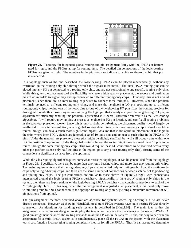
26
A
1 2
B
21 2 1 2 1
1 2 1 2 12
212121
121212
Figure 23. Topology for integrated global routing and pin assignment (left), with the FPGAs at bottomused for logic, and the FPGAs at top for routing only. The detailed pin connections of the logic-bearingFPGAs are given at right. The numbers in the pin positions indicate to which routing-only chip that pinis connected.
In a topology such as the one described, the logic-bearing FPGAs can be placed independently, without anyrestriction on the routing-only chip through which the signals must move. The inter-FPGA routing pins can beplaced into any I/O pin connected to a routing-only chip, and are not constrained to any specific routing-only chip.While this gives the placement tool the flexibility to create a high quality placement, the source and destinationpins of an inter-FPGA signal may end up connected to different routing-only chips. Obviously, this is not a validplacement, since there are no inter-routing chip wires to connect these terminals. However, since the problemterminals connect to different routing-only chips, and since the neighboring I/O pin positions go to differentrouting-only chips, moving one of the logic pins to one of the neighboring I/O pins fixes the routing problem forthis signal. While this move may require moving the logic pin that already occupies the neighboring I/O pin, analgorithm for efficiently handling this problem is presented in [Chan93] (hereafter referred to as the Clos routingalgorithm). It will require moving pins at most to a neighboring I/O pin location, and can fix all routing problemsin the topology presented above. Since this is only a slight perturbation, the placement quality should largely beunaffected. The alternate solution, where global routing determines which routing-only chip a signal should berouted through, can have a much more significant impact. Assume that in the optimum placement of the logic inthe chip, where inter-FPGA signals are ignored, a set of 10 logic pins end up next to each other in the FPGA’s I/Opins. Under the method just presented, these pins might be slightly shuffled, but will still occupy pins within oneI/O pin position of optimum. Under the global router solution, the router might have assigned these 10 pins to berouted through the same routing-only chip. This would require these I/O connections to be scattered across everyother pin position (since only half the pins in the region go to any given routing-only chip), forcing some of theconnections a significant distance from the optimum.
While the Clos routing algorithm requires somewhat restricted topologies, it can be generalized from the topologyin Figure 23. Specifically, there can be more than two logic-bearing chips, and more than two routing-only chips.The main requirements are that the logic-bearing chips are connected only to routing-only chips, the routing-onlychips only to logic-bearing chips, and there are the same number of connections between each pair of logic-bearingand routing-only chips. The pin connections are similar to those shown in Figure 23 right, with connectionsinterspersed around the logic-bearing FPGA’s periphery. Specifically, if there are N routing-only chips in thesystem, then there are N-pin regions on the logic-bearing FPGA’s periphery that contain connections to each of theN routing-only chips. In this way, when the pin assignment is adjusted after placement, a pin need only movewithin this group to find a connection to the appropriate routing-only chip, yielding a maximum movement of N-1pin positions from optimal.
The pin assignment methods described above are adequate for systems where logic-bearing FPGAs are neverdirectly connected. However, as show in [Hauck98], most multi-FPGA systems have logic-bearing FPGAs directlyconnected. An algorithm for handling such systems is described in [Hauck94]. The main idea is that pinassignment is just a process designed to simplify the interaction between the placements of connected FPGAs. Agood pin assignment balances the routing demands in all the FPGAs in the systems. Thus, one way to perform pinassignment for a multi-FPGA system is to simultaneously place all the FPGAs in the system, with the placementtool’s cost function incorporating routing complexity metrics for all the FPGAs. Thus, it can accurately determine

27
whether the benefit of a pin positioning in one FPGA is worth the routing problems it causes in connected FPGAs.However, since placement of a single FPGA is a very complex, time-consuming process, complete placement oftens to thousands of FPGAs simultaneously is intractable. The solution adopted is to simplify the placementprocess during the pin assignment stage, retaining only enough information to produce a reasonable assignment.After this step is done the individual FPGA mappings are developed independently by standard FPGA placementand routing tools, since once pin assignment is completed all inter-chip issues have been resolved.
The placement simplification process for pin assignment is based on properties of force-directed placement. Force-directed placement is a circuit placement technique that attempts to minimize wirelength by replacing all nets inthe system by springs, and then seeking the minimum net force placement [Shahookar91]. This tends to make thesprings shorter, which tends to make the nets shorter. In [Hauck94] it is shown that by removing the restrictionthat logic must be put into exact, unique function block locations, the rules of physics can be used to remove all thelogic from the mapping. In this process, the springs connected to a logic node during force-directed placement canbe replaced with springs connected only to the logic node’s neighbors. However, these neighbors see exactly thesame forces as if the logic block was still part of the mapping. Thus, by repeated application of these springreduction rules, all of the logic blocks can be removed from consideration. This leaves IOBs (connections from anFPGA to the rest of the system) interconnected by springs as if the entire mapping was still there. Thus, force-directed placement can then be applied to this simplified mapping quite efficiently, and a good quality pinassignment can be developed. Note that by removing the restriction on logic node placement, this pin assignmentapproach uses an inexact placement model. However, this reduction in local accuracy tends to be more than madeup for in the ability to seek the global optimum. Also, subsequent single-FPGA placement runs will be made to fixup this inaccuracy.
4.5 Logic Resynthesis
Multi-FPGA systems often require a logic resynthesis step before the other mapping phases. One view of logicresynthesis is that it is akin to technology mapping. Logic resynthesis is a transformation step that attempts tocreate a match between components in the user design and those available in the multi-FPGA hardware substrate.For example, user designs typically contain wide, deep, multiported memories, while those available in thehardware substrate are often single ported and narrow. This section discusses typical logic restructuringtransformations for memory and tristate nets.
In many systems, small single-ported memories can be treated much like any other combinational block to bemapped to the system (for example, see [Sample94, Butts91]). Memory can be implemented using either FPGAmemory capabilities or external RAMs. However, memory sometimes presents implementation difficulties when itis too wide, multiported, or deep to fit within the memory of an FPGA.
When deep memories do not fit within the FPGA memory limits, external RAMs must be used. This can oftenexacerbate pin limits. Wide memories can sometimes be handled by slicing wide memories into many narrowermemories, each of which is implemented in a narrower physical RAM and associated FPGAs. Slicing distributesthe data signals to multiple FPGAs, and can reduce the pin requirements of individual FPGAs. Slicing stillnecessitates the address to be routed to multiple FPGAs and memories. Multiported memories can be implementedin physical multiported memories, or they can be implemented by making multiple copies of the physical memoryto allow simultaneous access. Karchmer and Rose [Karchmer94] describe packaging algorithms for area efficientand delay-minimal packing of logical memories into physical memories.
An alternative approach might make use of a memory clock to simulate the effect of a multiported memory from asingle physical memory. The memory clock makes multiple transitions during each cycle of the user's design clockand allows a port to be accessed on each memory clock cycle. The memory clock can also be used to simulate awide memory using a narrower physical memory. Note, however, that systems must support the full width of thememory bus between the clocked memory system and the user's logic, and also provide a mechanism forsynchronizing user access with the memory clock.
VirtualWire systems tightly integrate memories with the virtual clock and multiplex the FPGA-memory path[Agarwal95]. Memories have an impact on various stages of VirtualWire systems software. A wide, multiported

28
user memory is first sliced into many multiported memory slices, each of which has a data bus width that is thesame as that of the physical RAMs. The address bus and control signals are connected to each of the slices. Theplacer locates the memory slices in physical RAMs and a corresponding associated FPGA that is physicallyconnected to the RAM. The placer must satisfy the constraint that the sum of the logical memory sizes assigned toeach physical memory do not exceed the size of physical memory.
The VirtualWire scheduler integrates memory scheduling into the normal scheduling and routing flow. When theaddress is available on the FPGA physically connected to the RAM, the compiler schedules memory-slice read orwrite cycles. The memory scheduler is also responsible for collecting the full memory word potentially frommultiple slices from multiple physical RAMs into a VirtualWire register and routing the data word so it isavailable where needed. The associated memory scheduling logic and state machines created according to thescheduling step are placed in FPGAs that are physically connected to the RAMs.
Memories are not the only components of an input netlist that may need to be altered to fit into a multi-FPGAsystem. Inside an FPGA, most signals are unidirectional, with a single source. In an input netlist, some signals(particularly buses and other tristate structures) may have multiple possible sources, and mapping such structuresdirectly to a multi-FPGA system may be difficult, especially if the sources of the net are computed on differentchips. Butts and Batcheller [Butts91] present a method for translating tristate nets into unidirectional nets.Suppose each tristate gate driving a tristate bus has a signal output O and a tristate enable signal E. All outputs Oof the tristate gates are combined into a single net. Such tristate nets are restructured using AND-OR gates, byreplacing each tristate gate with an AND gate whose inputs are E and O, and whose output is connected to theinput of a wide OR gate (see Figure 24). The output of the OR gate becomes the value of the tristate signal. In thisway, non-unidirectional signals can be fit into normal FPGA routing structures.
E1
I1
O1
E2
I2
O2
E3
I3
O3
E1
I1
O1
E2
I2
O2
E3
I3
O3
Figure 24. Tristate buses (left) in circuits mapped to multi-FPGA systems can be converted to a logicstructure with only single-source nets (right) [Butts91].
5.0 Software Support for Reconfigurable Computing
Normally, digital hardware designers create circuits by manipulating Boolean logic, by interconnecting logic gatesor transistors, or perhaps by writing a program in a hardware description language such as Verilog or VHDL.These methods of expressing hardware concepts are all applied to FPGA implementation. Each of thesedescription methods is designed to represent hardware concepts efficiently, and can model most important aspectsof circuit functionality.
Reconfigurable systems offer the ability to create extremely high-performance implementations for many differenttypes of applications. While techniques such as logic emulation provide a new tool specifically for logic designers,many other uses of FPGA-based systems serve as high-performance replacements for standard computers andsupercomputers. For such applications, the creators of these implementations will largely be softwareprogrammers, not hardware designers. However, if these systems hope to be useable by software programmers, thesystems must be capable of translating applications described in standard software programming languages intoFPGA realizations. Thus, mapping tools that can synthesize hardware implementations from C, C++, FORTRAN,or assembly language descriptions must be developed.
Although techniques exist to transform specifications written in hardware description languages into electroniccircuits, translating a standard software program into hardware presents extra challenges. Hardware description

29
languages focus mainly only constructs and semantics that can be efficiently translated into hardware (though eventhese languages allow the creation of non-synthesizeable specifications). Software programming languages haveno such restrictions. For example, hardware is inherently parallel, and hardware description languages have anexecution model that easily expresses concurrency. Most standard software languages normally have a sequentialexecution model, with instructions executing one after another. This means that a hardware implementation of asoftware program is either restricted to sequential operation, yielding an extremely inefficient circuit, or themapping software must figure out how to parallelize an inherently sequential specification. Also, there areoperations commonly found in software programs that are relatively expensive to implement in hardware. Thisincludes multiplication and variable-length shifts, as well as floating point operations. Although hardware can besynthesized to support these operations, software that makes extensive use of these operations will result inextremely large designs. Finally, software algorithms operate on standard-sized data values, using 8, 16, 32, or 64bit values even for operations that could easily fit into smaller bit-widths. By using wider than necessary operands,circuit datapaths must be made wider, increasing the hardware costs. Thus, because we are using a languagedesigned for specifying software programs to create hardware implementations the translation software faces amapping process more complex than for standard hardware description languages.
There have been many research projects that have developed methods for translating code in C [Athanas93,Wazlowski93, Agarwal94, Wo94, Galloway95, Isshiki95, Peterson96, Clark96, Yamauchi96], C++ [Iseli95], Ada[Dossis94], Occam [Page91, Luk94], data parallel C [Gokhale93, Guccione93], Smalltalk [Pottier96], Assembly[Razdan94a, Razdan94b] or other special hardware description languages [Singh95, Brown96] into FPGArealizations. These systems typically take software programs written in a subset of the programming language,translate the data computations into hardware operations, and insert multiplexing, latches and control statemachines to recreate the control flow. As mentioned earlier, software programming languages contain constructsthat are difficult to handle efficiently in FPGA logic. Because of this, each of the previous techniques restricts thelanguage constructs that can be present in the code to be translated. Most do not allow multiplication, division, orfloating point operations. Some ban the use of structures, pointers, or arrays [Wazlowski93, Agarwal94,Galloway95], eliminate recursion [Galloway95] or do not support function calls [Wo94] or control flow constructssuch as case, do-while, and loops without fixed iteration counts [Athanas93]. Some techniques, which areintended primarily to compile only short code sequences, may restrict data structures to only bitvectors [Iseli95], ornot support memory accesses at all [Razdan94a, Razdan94b]. Other techniques, such as that of Bertin and Touati[Bertin94], extend C++ for use as a hardware description language.
Translating straight-line code from software languages into hardware is relatively simple. Expressions in the codehave direct implementations in hardware that can compute the correct result (they must, since a processor onwhich the language is intended to run must have hardware to execute it). Variables could be stored in registers,with the result from each instruction latched immediately, and one instruction executing at a time. However, thisloses the inherent concurrency of hardware. We can instead combine multiple instructions together, only latchingthe results at the end of the overall computation. For example, the instructions “A = B + C; D = A - E;” can betranslated into “A = B + C; D = B + C - E;”, with all instructions occurring within a single clock cycle. Thecomputation of A could also be dropped if it is not used later in the code. Note that the reassignment of a value toa variable already used, such as “B = A + 1; A = A - C; D = A + 3;”, can be a problem, since the value of A in thefirst and third instruction are different. Renaming is a standard compiler technique for parallelizing such code, avariant of which is contained in the Transmogrifier C compiler [Galloway95]. The compiler moves sequentiallythrough a straight-line code sequence, remembering the logic used to create the value of each assignment.Variables in an assignment that comes from outside this piece of code draw their values from registers for thatvariable. Variables that have been the target of an assignment in the code sequence are replaced with the outputfrom the logic that computes its value earlier in the sequence. Thus, the sequence “B = A + 1; A = A - C; D = A +3;” becomes “B = A + 1; A’ = A - C; D = (A - C) + 3;”. With this logic construction the computation for allvariables can occur simultaneously. All the results would then be latched simultaneously, allowing them to bestored for further computations.
Because of the way assignments are handled, simple “if” statements can also be folded into a logic equation. Forexample, the C statement “if (condition) A = B;” becomes “A’ = (condition and B) or (not(condition) and A);”.The condition of the “if” statement turns into a multiplexor, assigning the result of the “then” clause to the variable

30
if the condition is true, or the “else” clause (or old value if there is no “else” clause) if the condition is false. In thisway, the jumps that would be necessary to implement the “if” statement are removed, increasing the size of straightline code segments. Obviously, if the “if” clause contains function calls or memory accesses (operations whichmay have side effects) this transformation cannot be done, and the “if” statement must be handled as more generalcontrol flow.
Loop unrolling can be used to turn loops with a constant number of iterations into straight line code. If a loop willbe executed N times, it is converted into N copies of the loop body, concatenated from iteration 1 to iteration N. Ifthe loop index is used inside the code, the index is assigned the appropriate value before each loop body. Also,local variables may need to be renamed within each loop body. The transformations described above can then beapplied to execute all of the instructions from the loop bodies in parallel.
For more complex control flow, such as loops which execute a variable number of times or “if” statementscontaining function calls, control state machines must be implemented (see Figure 25). The code is broken intoblocks of straight-line code. Each of these code segments is represented by a separate state in the control statemachine. The straight-line code is converted into logic functions as described above, with the series of operationscollapsed into a combinational circuit. Variables whose scope spans code segments are held in registers. Theinput to the register is a mux which combines the logic for assignment statements from different code sequences.For example, if the assignment statement “A = X;” is in code sequence 1, and “A = Y;” is in code sequence 2, thenthe logic driving the mux is “A = (X and state1) or (Y and state2) or (A and not (state1 or state2));”, where state1is the state corresponding to code sequence 1, and state2 corresponds to code sequence 2. If a given code sequenceuses that variable, the register’s output is fed to the corresponding logic.
/* state s1 */ x = y; while (x) { /* state s2 */ x = x - 2; } /* state s3 */ x = 12;
x == 0
x != 0
s3
s1
s2
x != 0
x == 0
000 100 010 001
s1 s2 s3
XY
subtract212
Figure 25. Example of variables and complex control flow. The code segment (left) is converted into acontrol state machine (center) and logic for controlling the variable’s register (right). Although the statesare shown in the code, these are automatically inferred from the control flow.
The control state machine is constructed to mimic the control flow in the source code. A “for” loop (where theloop test is executed before every iteration of the loop, including the first) is translated into a state for the codebefore the loop, one for the loop test, another for the loop body, and a final state for the code following the loop.The state machine has the test state always following both the pre-loop and loop body state, while the loop bodystate follows the test state if the loop test is true, and the post-loop state follows the test state if the test is false. Inthis way, loops without fixed loop bounds can be directly implemented in hardware. Complex “if” statements canbe handed similarly; The “then” and “else” bodies each have their own state, with the “then” state occurring afterthe pre “if” state if the clause is true, and the “else” state occurring otherwise. Both of these states then lead to thepost “if” state.
Function calls in the code require more careful construction. One might be tempted just to inline the function,making it part of the caller’s code. However, this means that some frequently used code sequences will beduplicated in many places, increasing the size of the hardware. An alternative is contained in the TransmogrifierC compiler [Galloway95]. Each function has its own control state machine, with a unique entry and exit state.The caller has a state before and after the function call, and once it reaches the state before the function call it tellsthe function’s state machine to start in its entry state. The caller then waits for the function to reach its exit state,at which point the caller moves on to its state for after the function call. Although multiple callers will all see thefunction reach its exit state, since only one of the callers will be active in its pre function call state, only the currentcaller will proceed to its next state. Recursion is normally not allowed because of this construction (since multiple

31
callers of the same function might be waiting in the function call state at the same time), as well as the need tohave separate logic for each recursive call to the function body.
func (int X, int Y) { /* state f1 */ x = y; /* state f2 */ } main() { /* state s1 */ func(a, 12); /* state s2 */ . . . /* state s100 */ func (b, 19); /* state s101 */ }
s100
s101
f2
!f2
s1
s2
f2
!f2
f1
f2
s1 s100
Figure 26. A code segment with a function call (left) is converted into a separate FSM for each procedure(right), with appropriate communication between components.
Once the controller for the hardware is constructed, techniques can be applied to simplify this state machine[Agarwal94]. States can be combined together sequentially or in parallel, allowing greater concurrency in thehardware, as well as minimizing the hardware cost of the controller. However, an even more important issue is thesimplification of the datapath, something that hasn’t yet been adequately addressed. In the construction givenabove every operation in the source code generates unique hardware. For simple computations this is fine.However, complex operations such as multiplication and division will be scattered throughout the source code,implying that a huge amount of hardware will be needed to implement all of these computations. However, each ofthe multipliers will only be used within the state corresponding to that portion of the source code, and otherwisewill sit idle. The circuit’s size could be greatly reduced if these hardware multipliers were reused in differentplaces in the code. A single hardware multiplier can be used for many separate multiplication operations from thesource code, as long as each of the multiplications occurs in different states. Thus, a 1000 line program, which has50 multiplications, would require 50 separate hardware multipliers in the current scheme. However, the 1000 lineprogram might be broken into 100 different states, with at most 4 multiplications occurring in any one state. Withthe proper muxing of the inputs to the hardware multipliers based on the state, only 4 hardware multipliers areactually required. Methods for performing such alterations are already available for the compilation of hardwaredescription languages, and similar transformations are important for efficiently converting software programminglanguages into FPGA realizations.
There are several different systems that convert code sequences in software programming languages into hardwarerealizations. While they all support the translation of control flow and datapath operations into circuits, they differon the amount of code they convert, and the model of operation they assume. Perhaps the most straightforward isthe Transmogrifier C system [Galloway95]. This system takes a complete program written in the C programminglanguage and translates it into a circuit directly implementable in the CLBs of Xilinx FPGAs. Special pragma(compiler directive) statements are included to declare external inputs and outputs, including the assignment ofthese communications to specific FPGA pins. This yields a system where the resulting hardware implementation isexpected to be a complete, self-contained system implementing the entire functionality of the desired behavior.
Most of the systems for translating software programs into hardware algorithms assume that only the most time-critical portions of the code are mapped to the FPGAs [Athanas93, Wazlowski93, Agarwal94, Razdan94a,Razdan94b, Wo94, Iseli95, Clark96]. These systems use the FPGA(s) as a coprocessor to a standard CPU. Theprocessor implements most of the program, handling much of the operations that are necessary to implement
32
complex algorithms, but which contribute little to the total computation time. The truly time-critical portions ofthe algorithm are translated into hardware, using the FPGA to implement the small fraction of the total codecomplexity which accounts for most of the overall runtime. In this way the strengths of both FPGAs and standardprocessors are combined into a single system. Processors can easily implement a large variety of operations byworking through a complex series of instructions stored in high-density memory chips. Mapping all of theseinstructions into FPGA logic means that the complete functionality of the entire program must be availablesimultaneously, using a huge amount of circuit space. However, we can implement only the most frequently usedportions of code inside the FPGA, achieving a significant performance boost with only a small amount ofhardware. During the execution of the program the processor executes the software code until it hits a portion ofthe code implemented inside the FPGA coprocessor. The processor then transfers the inputs to the function to theFPGA coprocessor and tells it to begin computing the correct subroutine. Once the FPGA has computed thefunction, the results are transferred back to the processor, which continues on with the rest of the software code.An added benefit of the coprocessor model is that the software to hardware compiler does not have to support alloperations from the software programming language, since complex functions such as multiplication or memoryloads can be handled instead by the host processor. This does limit the portions of the code that can be translatedinto hardware. However, a system which converts the complete program into hardware must either convert theseoperations into FPGA realizations, yielding much larger area requirements, or must ban these constructs from thesource code, limiting the types of operations and algorithms that can be supported.
Although compiling only the critical regions of a software algorithm can reduce the area requirements, and avoidhardware-inefficient operations, it does introduce problems unique to these types of systems. One problem is thatthere must be some mechanism introduced for communicating operands and results between the processor and thecoprocessor. For systems like PRISC [Razdan94a, Razdan94b], which view the FPGA as merely a mechanism forincreasing the instruction set of the host processor, instructions are restricted to reading from two source registers,and writing one result register, just like any other instruction on the processor. However, other systems have muchless tightly coupled FPGAs, and require protocols between the two systems. In the PRISM systems [Athanas93,Wazlowski93, Agarwal94] up to 64 bits may be sent across the bus to the coprocessor, which then beginscomputing. In both of these systems, the communication mechanism puts a hard limit on the amount ofinformation that can be communicated, and thus the amount of the computation that can be migrated to hardware.For example, if only two input words and a single output word are allowed, there is obviously only so much usefulcomputation that can be performed in most circumstances.
A second important issue with compiling only a portion of a program into hardware is determining which portionsof the code to so map. Obviously, the code that gets mapped to the hardware needs to contain a large portion of theruntime of the overall algorithm if we hope to achieve significant performance improvements. However, it isdifficult to determine where the critical portions of a program are strictly from the source code. In general, thesolutions are to profile the execution of the software on a sample input set to find the most frequently executed codesequences [Razdan94a, Razdan94b], or to have the user pick the code sequences to use by hand [Athanas93,Wazlowski93, Agarwal94, Wo94]. However, simply identifying the most often executed code sequences may notyield the best speedups. Specifically, some code sequences will achieve higher performance improvements thanothers when mapped to hardware. For example, even though a given code sequence occurs twice as much asanother, if the achieved speedup is only a quarter of what is possible for the other sequence the other sequence isthe better routine to optimize. Also, some code sequences may be too complex to map into hardware, not fittingwithin the logic resources present in the FPGA. The PRISC compiler [Razdan94a, Razdan94b] performs somesimple checks to see whether a given code sequence will fit in the FPGA resources, and will reduce the amount ofcode translated if the current selection will not fit. However, in general greater automation of this decision processis necessary.
6.0 Software Support for Run-Time Reconfigurability
Perhaps one of the types of systems most unique to FPGAs is run-time reconfigurability. The idea is that since anFPGA is reconfigurable, its programming can be changed while the system is still executing. Thus, like the virtualmemory in a normal processor, a run-time-reconfigurable FPGA can be viewed as “Virtual Hardware”, paging

33
hardware into the FPGA only when it is needed, and allowing large systems to be squeezed into a relatively smallamount of physical hardware.
While the concept of run-time reconfigurability is quite promising, there are many issues that must be consideredin developing such a system. Since the configuration of an FPGA can change dynamically, and in fact someportions of the FPGA may be changing while others are performing useful work, it becomes difficult to understandthe exact behavior of the system. The logic must be designed so that it only accesses those logic subcircuits thatare currently loaded into the FPGA, and must properly ignore spurious signals from unconfigured or reconfiguringsections of the FPGA.
TASK_A
TASK_B
TASK_D
TASK_A
TASK_C
TASK_D
Figure 27. Conceptual diagram of a run-time reconfigurable system, with fixed logic tasks “A” and “D”,and tasks “B” and “C” which are swapped in and out during the operation of the circuit [Lysaght96].
As an aid in the development of run-time reconfigurable systems, Lysaght and Stockwood have developed asimulation approach for these systems [Lysaght96]. In their methodology, a circuit’s VHDL description isannotated with information on what signals will cause a given subcircuit to be loaded into hardware, and how longthe reconfiguration process takes. This initial description is then automatically transformed into a new descriptionwith explicit isolation switches between the subcircuits controlled by schedulers based upon the circuit annotations.Whenever a given component should not be present in the FPGA, or has not yet been completely loaded into thechip, these isolation switches set the value of all of that subcircuit’s signals to unknown (“X”). Thus, any circuitrythat is (erroneously) sensitive to the value of signals from circuitry that is not currently loaded will also go to theunknown state, demonstrating the logical flaw. When the circuit is properly loaded into the FPGA, the isolationswitches simply forward on all signal values. This new representation of the circuit can now be simulatednormally, allowing standard software simulators to support the execution of run-time-reconfigurable systems.Another method for simulating run-time reconfigurable systems in VHDL has been proposed by Kwait and Debany[Kwait96].
Scheduler
TASK_BTASK_A
TASK_CTASK_D
Figure 28. Simulation model for the circuit of Figure 27. Isolation switches (grey squares) and areconfiguration scheduler are added to the base VHDL description to mimic the reconfigurationoperations [Lysaght96].
The modeling of unconfigured or reconfiguring outputs with the unknown value allows the user to test the logicalcorrectness of their design. However, one issue that is not addressed by this is the electrical correctness of a circuit.Specifically, in many FPGAs there are long-distance communication lines which have tristate drivers allowingmultiple different logic blocks to drive the line. Normally, when developing a configuration for an FPGA thedesign software ensures that at most one logic block is configured to drive a given wire. Otherwise, with multiplewriters to a single wire a direct power-ground connection can be set up, potentially overheating and destroying thechip. However, with dynamic reconfiguration the writer of the wire may change, since different configurationsmay require a different interconnection scheme. As long as configurations with different writers to the same lineare never allowed to coexist in the chip, this is a legal design. However, it may be difficult to determine whether

34
two configurations, with conflicting writer assignments, will ever coexist in the chip. Even worse, when thesystem switches between configurations, parts of the new and the old configuration may coexist briefly, sincereconfiguring an FPGA is not an instantaneous, atomic process. To deal with this, the Lysaght and Stockwoodwork [Lysaght96] suggests that an old configuration first be overwritten by a “safe” configuration before loadingthe new configuration. Thus, this “safe” configuration would turn off all drivers to shared resources, avoiding thepartial configuration conflicts. However, the more general issue of how to ensure that two configurations withconflicting writer assignments are never loaded simultaneously is still an important open problem.
There are many other open problems in the design of run-time reconfigurable systems, with almost no currentsolutions. Current software support for standard reconfigurable systems is largely useless for this domain, sincethey do not have any support for time-varying mappings. To some extent, the challenges of run-timereconfigurability are similar to those of self-modifying code. Since the configuration changes over time, under thecontrol of the configuration itself, there needs to be some way to make sure that the system behaves properly for allpossible execution sequences. This is in general a challenging problem to address.
Beyond just issues of making sure that a run-time reconfigurable system behaves properly, producing a functionallyand electrically correct implementation of the desired behavior, there are some major issues in how to produce thebest possible implementation of the functionality. With normal FPGA-based systems, one wants to map the logicspatially so that it occupies the smallest area, and produces results as quickly as possible. In a run-timereconfigurable system one must also consider the time to reconfigure the system, and how this impacts theperformance of the system. Configuration can take a significant amount of time, and thus reconfiguration shouldbe kept to a minimum. Thus, it will be critical to group logic together properly so that a given configuration cando as much work as possible, allowing a greater portion of the task to be completed between reconfigurations. Onepossibility already implemented is to group together all instructions from the same function in a software algorithmand put them into their own separate context [Gokhale95]. However, what to do when function boundaries are toolarge or too small is still unclear. Techniques also need to be developed for limiting the amount of data that mustbe changed during reconfiguration. One possibility is to better encode the configuration information, requiringfewer bits to configure the FPGA, and thus reduce the reconfiguration time [DeHon96]. Another is to maximizesimilarity between configurations. For example, if several configurations all require an 8-bit multiplier, and thatmultiplier is placed into the same location in the FPGA in all configurations, then this portion of the FPGA willnot need to be reconfigured when switching between these configurations. Such techniques may be able tosignificantly reduce the reconfiguration overhead, improving the performance of run-time reconfiguration, andthus increasing its applicability.
7.0 Conclusions
While hardware substrates are an important area of research for reconfigurable computing, efficient softwaresupport for automatically mapping applications to these systems is critical to their being widely accepted. Forsome of these tasks standard single-FPGA mapping tools can be harnessed for reconfigurable systems.Reconfigurable systems must perform technology mapping, placement and routing, which requires similaroptimizations to normal FPGAs. However, for complete reconfigurable systems other optimizations must beperformed, and these optimizations must handle the constraints of reconfigurable systems. For example, multi-FPGA systems have fixed inter-FPGA routing structures, requiring careful consideration of partitioning, globalplacement, and global routing tasks. Also, logic restructuring may need to be performed to alter the input netlistinto a form that can be accommodated within the reconfigurable system. Finally, limited inter-chip bandwidth andscalability considerations may require special optimizations, such as the VirtualWires methodology for time-multiplexing FPGA I/O pins and scheduling signals according to a discrete time base.
Reconfigurable mapping software differs from standard hardware compilers and CAD algorithms not just becauseof the constraints of FPGA-based implementations, but also due to the types of users these systems hope to support.For reconfigurable computing, a reconfigurable system is used as a replacement for a standard computer, providinga high-performance implementation medium. Accordingly, these systems must support input formats familiar tosoftware programmers, including C and other standard software languages. As we discussed, there are severalsystems for converting standard software algorithms into FPGA-based implementations. However, most of these

35
systems are quite restricted, limiting the constructs allowed in the input. Also, for systems which include bothreconfigurable and standard microprocessor components, tools are needed to determine which parts of analgorithm should be mapped into hardware, and which should remain software; Currently, such techniques havenot been completely developed.
Run-time reconfigurable systems face even greater challenges. Allowing the configuration of the FPGAs in asystem to change over time, even to the level of changing subregions of the FPGA while the rest of the systemcontinues operating, creates many new issues for software tools to address. While there have been some toolsdeveloped for simulating these systems, methods for detecting erroneous configurations, automatically schedulingreconfiguration, and placing logic to minimize the amount of reconfiguration necessary, all still need to bedeveloped.
In general, there are significant opportunities for future innovating in software support for reconfigurable systems.Techniques must be developed for performing partitioning and global routing in arbitrary topologies. Current toolstend to be focused on specific topologies (primarily crossbars and partial crossbars), limiting the types of systemsthat can be supported. Mapping tools for structured netlists may also be able to greatly improve reconfigurablesystems; Current tools treat the input circuit as random logic, missing opportunities for optimization based on thestructure of regular datapaths, hierarchical circuits, and other non-random components.
Perhaps one of the most unique considerations of reconfigurable systems, as opposed to standard hardwareimplementations, is the need for high-performance mapping tools. Normal VLSI implementations take months todevelop the circuit design, and weeks for the fabrication. Thus, mapping times of a few days are acceptable. Forreconfigurable systems, systems which can be programmed to implement a desired behavior in a matter ofmicroseconds, mapping times of days limit the usefulness of these systems. For logic emulation systems, which areused in a testing-debug-retesting methodology, mapping times of a day or more are common, and thus limit theturnaround time for design changes. For custom computing systems, software programmers accustomed tocompile times of minutes to tens of minutes may be unwilling to accept mapping times an order of magnitudelonger. Thus, along with the development of algorithms to support tasks not covered by current software,development of faster mapping times will be a primary concern for future reconfigurable system compilers.Techniques such as incremental update, where small changes in an input circuit cause only minor recompilation ofthe mapping, can greatly speed up mapping tools. Also, tools which can trade quality for compile time may beuseful for this domain, allowing the circuit developer the choice of how long to wait for their implementation. Ofcourse, new FPGA architectures that admit better compile times and are better suited for reconfigurable computingmust also be developed.
The move towards automating the mapping process must always strike a balance between ease of design and thequality degradation of the results. In a system like a logic emulator it is clear that a fully automatic mappingsystem is the only reasonable method for using such a system. However, for custom-computing devices there willalways be room for hand-mapping of applications, just as in general-purpose software development some criticalcomponents will always be written in assembly language. The hope in the FPGA-based computing community isto develop mapping tools that achieve a level of quality approaching that of hand-mapping, and transition manyFPGA-based systems to a partially or wholly automatic mapping system. How successful such efforts are dependslargely on the quality of the results generated. However, without such an automatic mapping solution for at leastsome designs, the benefits of FPGA-based systems will be denied to a large user base that is unwilling to learn howto perform the complete hand-mapping of applications to this substrate.
In summary, the challenges of reconfigurable systems are unlike those of other systems. Their restrictedinterconnect, demand for fast compile times, and scheduling concerns of run-time reconfiguration provideoptimization goals different from standard hardware implementations, while their fine-grained parallelism and lowlevel programmability are much different from the implementation realities of standard processors. While therehas been significant work on software tools specifically optimized to reconfigurable systems, there are manyremaining issues in the development of a complete hardware and software reconfigurable system.

36
References[Abouzeid93] P. Abouzeid, B. Babba, M. C. de Paulet, G. Saucier, “Input-Driven Partitioning Methods and
Application to Synthesis on Table-Lookup-Based FPGA's”, IEEE Transactions on Computer-Aided Design of Integrated Circuits and Systems, Vol. 12, No. 7, July 1993.
[Adé94] M. Adé, R. Lauwereins, M. Engels, J. A. Peperstraete, “Communication Primitives on FPGAsin a Heterogeneous Multi-processor Emulation Environment”, in W. Moore, W. Luk, Eds.,More FPGAs, Oxford, England: Abingdon EE&CS Books, pp. 170-181, 1994.
[Agarwal91] A. Agarwal, “Limits on Interconnection Network Performance”, IEEE Transactions onParallel and Distributed Systems, Vol. 2, No. 4, pp. 398-412, October, 1991.
[Agarwal94] L. Agarwal, M. Wazlowski, S. Ghosh, “An Asynchronous Approach to Efficient Execution ofPrograms on Adaptive Architectures Utilizing FPGAs”, IEEE Workshop on FPGAs for CustomComputing Machines, pp. 101-110, 1994.
[Agarwal95] A. Agarwal, "VirtualWires: A Technology for Massive Multi-FPGA Systems",http://www.ikos.com/products/virtualwires.ps, 1995.
[Alpert95] C. J. Alpert, A. B. Kahng, "Recent Directions in Netlist Partitioning: A Survey", Integration:the VLSI Journal, Vol. 19, No. 1-2, pp. 1-81, 1995.
[Aptix93] Aptix Corporation, Data Book, San Jose, CA, February 1993.[Arnold94] J. M. Arnold, D. A. Buell, “VHDL Programming on Splash 2”, in W. Moore, W. Luk, Eds.,
More FPGAs, Oxford, England: Abingdon EE&CS Books, pp. 182-191, 1994.[Athanas93] P. M. Athanas, H. F. Silverman, “Processor Reconfiguration Through Instruction-Set
Metamorphosis”, IEEE Computer, Vol. 26, No. 3, pp. 11-18, March, 1993.[Babb93] J. Babb, R. Tessier, A. Agarwal, “Virtual Wires: Overcoming Pin Limitations in FPGA-based
Logic Emulators”, IEEE Workshop on FPGAs for Custom Computing Machines, pp. 142-151,1993.
[Bertin94] P. Bertin, H. Touati, “PAM Programming Environments: Practice and Experience”,Proceedings of the Second IEEE Workshop on FPGAs for Custom Computing Machines, pp.133-138, April 1994.
[Brayton85] R. Brayton, G. Hachtel, C. McMullen, A. Sangiovanni-Vincentelli, Logic MinimizationAlgorithms for VLSI Synthesis, Kluwer Academic, MA, 1985.
[Brown92a] S. D. Brown, R. J. Francis, J. Rose, Z. G. Vranesic, Field-Programmable Gate Arrays, Boston,Mass: Kluwer Academic Publishers, 1992.
[Brown92b] S. Brown, J. Rose, Z. G. Vranesic, “A Detailed Router for Field-Programmable Gate Arrays”,IEEE Transactions on Computer-Aided Design, Vol. 11, No. 5, pp. 620-628, May 1992.
[Brown96] G. Brown, A. Wenban, “A Software Development System for FPGA-Based Data AcquisitionSystems”, Proceedings of the Fourth IEEE Workshop on FPGAs for Custom ComputingMachines, April 1996.
[Butts91] M. R. Butts, J. A. Batcheller, Method of Using Electronically Reconfigurable Logic Circuits,United States Patent 5,036,473, July 30, 1991.
[Cai91] Y. Cai, D. F. Wong, “Optimal Channel Pin Assignment”, IEEE Transaction on Computer-Aided Design, Vol. 10, No. 11, pp. 1413-1424, Nov. 1991.
[Chan93] P. K. Chan, M. D. F. Schlag, “Architectural Tradeoffs in Field-Programmable-Device-BasedComputing Systems”, IEEE Workshop on FPGAs for Custom Computing Machines, pp. 152-161, 1993.
[Chan95] P. K. Chan, M. D. F. Schlag, J. Y. Zien, “Spectral-Based Multi-Way FPGA Partitioning”,ACM/SIGDA International Symposium on Field Programmable Gate Arrays, pp. 133-139,1995.
[Chang96] S.-C. Chang, M. Marek-Sadowska, T.-T. Hwang, “Technology Mapping for TLU FPGA'sBased on Decomposition of Binary Decision Diagrams”, IEEE Transactions on Computer-Aided Design of Integrated Ciruciuts and Systems, Vol. 15, No. 10, October 1996.
[Chen95] C.-S. Chen, Y.-W. Tsay, T.-T. Hwang, A. C.H. Wu, Y.-L. Lin, “Combining TechnologyMapping and Placement for Delay-Minimization in FPGA Designs", IEEE Transactions onComputer-Aided Design of Integrated Circuits and Systems, Vol. 14, No. 9, September 1995.

37
[Chou94] N.-C. Chou, L.-T. Liu, C.-K. Cheng, W.-J. Dai, R. Lindelof, “Circuit Partitioning for HugeLogic Emulation Systems”, Proceedings of the 31st Design Automation Conference, pp. 244-249, 1994.
[Clark96] D.A. Clark, B.L. Hutchings, “The DISC Programming Environment”, Proceedings of theFourth IEEE Workshop on FPGAs for Custom Computing Machines, April 1996.
[Cong91] J. Cong, “Pin Assignment with Global Routing for General Cell Designs”, IEEE Transactionon Computer-Aided Design, Vol. 10, No. 11, pp. 1401-1412, Nov. 1991.
[Cong92] J. Cong, Y. Ding, “An Optimal Technology Mapping Algorithm For Delay Optimization InLookup-Table Based FPGA Design”, International Conference on Computer-Aided Design,1992.
[Cong93] J. Cong, Y. Ding, “On Area/Depth Trade-off in LUT-Based FPGA Technology Mapping”,Design Automation Conference, pp. 213-218, 1993.
[DeHon96] A. DeHon, “Entropy, Couting, and Programmable Interconnect”, International Symposium onField Programmable Gate Arrays, pp. 73-79, 1996.
[Dossis94] M. F. Dossis, J. M. Noras, G. J. Porter, “Custom Co-processor Compilation”, in W. Moore, W.Luk, Eds., More FPGAs, Oxford, England: Abingdon EE&CS Books, pp. 202-212, 1994.
[Fang96] W.-J. Fang, A. C.-H. Wu, “A Hierarchucal Functional Structuring and Partitioning Approachfor Multiple-FPGA Implementations”, International Conference on Computer-Aided Design,pp. 638-643, 1996.
[Farrahi94] A. H. Farrahi, M. Sarrafzadeh, “Complexity of the Look-up Table Minimization Problem forFPGA Technology Mapping”, IEEE Transactions on Computer Aided Design, Vol. 13, No. 11,pp. 1319-1332, November 1994.
[Francis90] R. Francis, J. Rose, K. Chung, “Chortle: A Technology Mapping Program for Lookup Table-Based Field Programmable Gate Arrays”, Design Automation Conference, pp. 613-619, 1990.
[Francis91a] R. Francis, J. Rose, Z. Vranesic, “Chortle-crf: Fast Technology Mapping for Lookup Table-Based FPGAs”, Design Automation Conference, pp. 227-233, 1991.
[Francis91b] R. Francis, J. Rose, Z. Vranesic, “Technology Mapping for Lookup Table-Based FPGAs forPerformance”, International Conference on Computer-Aided Design, pp. 568-571, 1991.
[Frankle92] J. Frankle, “Iterative and Adaptive Slack Allocation for Performance-driven Layout and FPGARouting”, Design Automation Conference, pp. 539-542, 1992.
[Galloway95] D. Galloway, “The Transmogrifier C Hardware Description Language and Compiler forFPGAs”, IEEE Symposium on FPGAs for Custom Computing Machines, 1995.
[Gokhale93] M. Gokhale, R. Minnich, “FPGA Programming in a Data Parallel C”, Proceedings of the FirstIEEE Workshop on FPGAs for Custom Computing Machines, pp. 94-102, April 1993.
[Gokhale95] M. Gokhale, A. Marks, “Automatic Synthesis of Parallel Programs Targetted to DynamicallyReconfigurable Logic Arrays”, in W. Moore, W. Luk, Eds., Field-Programmable Logic andApplications, Berlin, Germany: Springer, pp. 399-408, 1995.
[Guccione93] S. A. Guccione, M. J. Gonzalez, “A Data-Parallel Programming Model for ReconfigurableArchitectures", Proceedings of the First IEEE Workshop on FPGAs for Custom ComputingMachines, pp. 79-87, 1993.
[Hauck94] S. Hauck, G. Borriello, “Pin Assignment for Multi-FPGA Systems (Extended Abstract)”, IEEEWorkshop on FPGAs for Custom Computing Machines, pp. 11-13, April, 1994. The completepaper appears as University of Washington, Dept. of CSE Technical Report #94-04-01, 1994.
[Hauck95a] S. Hauck, G. Borriello, “An Evaluation of Bipartitioning Techniques”, Chapel Hill Conferenceon Advanced Research in VLSI, pp. 383-402, March, 1995.
[Hauck95b] S. Hauck, G. Borriello, “Logic Partition Orderings for Multi-FPGA Systems”, ACM/SIGDAInternational Symposium on Field-Programmable Gate Arrays, pp. 32-38, February, 1995.
[Hauck98] S. Hauck, “The Roles of FPGAs in Reprogrammable Systems”, Proceedings of the IEEE, Vol.86, No. 4, pp. 615-639, April 1998.
[Huang95a] J. Huang, J. Jou, and W. Shen, “Compatible Class Encoding in Roth-Karp Decomposition forTwo-Output LUT Architectures”, International Conference on Computer-Aided Design, pp.359-363, 1995.

38
[Huang95b] D. J.-H. Huang, A. B. Kahng, “Multi-Way System Partitioning into a Single Type or MultipleTypes of FPGAs”, ACM/SIGDA International Symposium on Field Programmable GateArrays, pp. 140-145, 1995.
[Hwang94] T.-T. Hwang, R. M. Owens, M. J. Irwin, K. H. Wang, “Logic Synthesis for Field-Programmable Gate Arrays”, IEEE Transactions on Computer-Aided Design of IntegratedCircuits and Systems, Vol. 13, No. 10, October 1994.
[I-Cube94] I-Cube, Inc., “The FPID Family Data Sheet”, Santa Clara, CA, February 1994.[Iseli95] C. Iseli, E. Sanchez, “A C++ Compiler for FPGA Custom Execution Units Synthesis”, IEEE
Symposium on FPGAs for Custom Computing Machines, 1995.[Isshiki95] T. Isshiki, W. W.-M. Dai, “High-Level Bit-Serial Datapath Synthesis for Multi-FPGA
Systems”, ACM/SIGDA Symposium on Field-Programmable Gate Arrays, pp. 167-173, 1995.[Kadi94] M. Slimane-Kadi, D. Brasen, G. Saucier, “A Fast-FPGA Prototyping System That Uses
Inexpensive High-Performance FPIC”, ACM/SIGDA Workshop on Field-Programmable GateArrays, 1994.
[Karchmer94] D. Karchmer, J. Rose, “Definition and Solution of the Memory Packing Problem for Field-Programmable Systems”, Proceedings of ICCAD, pp. 20-26, 1994.
[Kernighan70] B. W. Kernighan, S. Lin, “An Efficient Heuristic Procedure for Partitioning of ElectricalCircuits”, Bell Systems Technical Journal, Vol. 49, No. 2, pp. 291- 307, February 1970.
[Kim96] C. Kim, H.Shin, “A Performance-Driven Logic Emulation Systems: FPGA Network Designand Performance-Driven Partitioning", IEEE Transactions on Computer-Aided Design ofIntegrated Circuits and Systems, Vol. 15, No. 5, May 1996.
[Kuznar93] R. Kuznar, F. Brglez, K. Kozminski, “Cost Minimization of Partitions into Multiple Devices”,Proceedings of the 30th Design Automation Conference, pp. 315-320, 1993.
[Kuznar94] R. Kuznar, F. Brglez, B. Zajc, “Multi-way Netlist Partitioning into Heterogeneous FPGAs andMinimization of Total Device Cost and Interconnect”, Design Automation Conference, pp.238-243, 1994.
[Kuznar95] R. Kuznar, F. Brglez, “PROP: A Recursive Paradigm for Area-Efficient and PerformanceOriented Partitioning of Large FPGA Netlists”, International Conference on Computer-AidedDesign, pp. 644-649, 1995.
[Kwait96] K. Kwait, W. Debany, “Reconfigurable Logic Modeling”, Integrated Systems Design, Vol. 8,Issue 90, pp. 18-28, December 1996.
[Legl96] C. Legl, B. Wurth, K. Eckl, “An Implicit Algorithm for Support Minimization DuringFunctional Decomposition”, European Design and Test Conference, 1996.
[Luk94] W. Luk, D. Ferguson, I. Page, “Structured Hardware Compilation of Parallel Programs”, in W.Moore, W. Luk, Eds., More FPGAs, Oxford, England: Abingdon EE&CS Books, pp. 213-224,1994.
[Luk95] W. Luk, “A Declarative Approach to Incremental Custom Computing”, Proceedings of theThird IEEE Workshop on FPGAs for Custom Computing Machines, pp. 164-172, April 1995.
[Lysaght96] p. Lysaght, J. Stockwood, “A Simulation Tool fpr Dynamically Reconfigurable FieldProgrammable Gate Arrays”, IEEE Transactions on VLSI Systems, Vol. 4, No. 3, pp. 381-390,September 1996.
[Mak95a] W.-K. Mak, D. F. Wong, “Board-Level Multi-Terminal Net Routing for FPGA-based LogicEmulation”, International Conference on Computer-Aided Design, pp. 339-344, 1995.
[Mak95b] W.-K. Mak, D. F. Wong, “On Optimal Board-Level Routing for FPGA-based LogicEmulation”, Design Automation Conference, 1995.
[Mathur95] A. Mathur, C. K. Chen, C. L. Liu, “Applications of Slack Neighborhood Graphs to TimingDriven Optimization Problems in FPGAs”, ACM/SIGDA International Symposium on FieldProgrammable Gate Arrays, pp. 118-124, 1995.
[McFarland90] M. C. McFarland, A. C. Parker, R. Camposano, “The High-Level Synthesis of DigitalSystems”, Proceedings of the IEEE, Vol. 78, N0. 2, pp. 301-318, February 1990.
[Murgai90] R. Murgai, Y. Nishizaki, N. Shenoy, R. K. Brayton, A. Sangiovanni-Vincentelli, “LogicSynthesis Algorithms for Programmable Gate Arrays”, Design Automation Conference, pp.620-625, 1990.

39
[Murgai91a] R. Murgai, N. Shenoy, R. K. Brayton, A. Sangiovanni-Vincentelli., “Improved Logic SynthesisAlgorithms for Table Look Up Architectures”, Design Automation Conference, pp. 564-567,1991.
[Murgai91b] R. Murgai, N. Shenoy, R. K. Brayton, A. Sangiovanni-Vincentelli, “Performance DirectedSynthesis for Table Look Up Programmable Gate Arrays”, International Conference onComputer-Aided Design, pp. 572-575, 1991.
[Murgai94] R. Murgai, R. K. Brayton, and A. Sangiovanni-Vincentelli, “Optimum FunctionalDecomposition Using Encoding”, Design Automation Conference, pp. 408-414, 1994.
[Page91] I. Page, W. Luk, “Compiling Occam into FPGAs”, in W. Moore, W. Luk, Eds., FPGAs,Abingdon, England: Abingdon EE&CS Books, pp. 271-283, 1991.
[Peterson96] J.B. Peterson, R.B. O'Connor, P.M. Athanas, “Scheduling and Partitioning ANSI-C Programsonto Multi-FPGA CCM Architectures”, Proceedings of the Fourth IEEE Workshop on FPGAsfor Custom Computing Machines, April 1996.
[Pförtner92] T. Pförtner, S. Kiefl, R. Dachauer, “Embedded Pin Assignment for Top Down System Design”,European Design Automation Conference, pp. 209-214, 1992.
[Pottier96] B. Pottier, J. Llopis, “Revisiting Smalltalk-80 blocks: A logic generator for FPGAs”,Proceedings of the Fourth IEEE Workshop on FPGAs for Custom Computing Machines, April1996.
[Raman94] S. Raman, C. L. Liu, L. G. Jones, “A Delay Driven FPGA Placement Algorithm”, EURO-DAC, pp. 277-82, 1994.
[Razdan94a] R. Razdan, PRISC: Programmable Reduced Instruction Set Computers, Ph.D. Thesis, HarvardUniversity, Division of Applied Sciences, 1994.
[Razdan94b] R. Razdan, M. D. Smith, “A High-Performance Microarchitecture with Hardware-Programmable Functional Units”, International Symposium on Microarchitecture, pp. 172-180, 1994.
[Roy-Neogi95] K. Roy-Neogi, C. Sechen, “Multiple FPGA Partitioning with Performance Optimization”,ACM/SIGDA Symposium on Field-Programmable Gate Arrays, pp. 146-152, 1995.
[Roy94] K. Roy, A Timing-Driven Multi-Way Partitioning System for Integrated Circuits and Multi-Chip Systems, Ph.D. Thesis, University of Washington, Dept. of EE, 1994.
[Sample94] S. J. Sample, M. R. D'Amour, T. S. Payne, Reconfigurable Hardware Emulation System,United States Patent 5,329,470, July 12, 1994.
[Sawada95] H. Sawada, T. Suyama, A. Nagoya, “Logic Synthesis for Lookup Table Based FPGAs UsingFunctional Decomposition and Support Minimization”, International Conference onComputer-Aided Design, pp. 353-358, 1995.
[Selvidge95] C. Selvidge, A. Agarwal, M. Dahl, J. Babb, “TIERS: Topology IndependEnt Pipelined Routingand Scheduling for VirtualWire™ Compilation”, ACM/SIGDA International Symposium onField-Programmable Gate Arrays, pp. 25-31, 1995.
[Shahookar91] K. Shahookar, P. Mazumder, “VLSI Cell Placement Techniques”, ACM Computing Surveys,Vol. 23, No. 2, pp. 145-220, June 1991.
[Shen95] W. Shen, J. Huang, S. Chao, “Lambda Set Selection in Roth-Karp Decomposition for LUT-Based FPGA Technology Mapping”, Design Automation Conference, pp. 65-69, 1995.
[Singh95] S. Singh, “Architectural Descriptions for FPGA Circuits”, Proceedings of the Third IEEEWorkshop on FPGAs for Custom Computing Machines, pp. 145-154, April 1995.
[Snider95] G. Snider, P. Kuekes, W. B. Culbertson, R. J. Carter, A. S. Berger, R. Amerson, “The TeramacConfigurable Compute Engine”, in W. Moore, W. Luk, Eds., Field-Programmable Logic andApplications, Berlin, Germany: Springer, pp. 44-53, 1995.
[Stanion95] T. Stanion, C.~Sechen, “A Method for Finding Good Ashenhurst Decomposition and itsApplication to FPGA Synthesis”, Design Automation Conference, pp. 60-64, 1995.
[Thomae91] D. A. Thomae, T. A. Petersen, D. E. Van den Bout, “The Anyboard Rapid PrototypingEnvironment”, Advanced Research in VLSI 1991: Santa Cruz, pp. 356-370, 1991.
[Togawa94] N. Togawa, M. Sato, T. Ohtsuki, “A Simultaneous Placement and Global Routing Algorithmfor Symmetric FPGAs”, ACM/SIGDA International Workshop on Field Programmable GateArrays, 1994.

40
[Van den Bout92] D. E. Van den Bout, J. N. Morris, D. Thomae, S. Labrozzi, S. Wingo, D. Hallman, “Anyboard:An FPGA-Based, Reconfigurable System”, IEEE Design & Test of Computers, pp. 21-30,September, 1992.
[Van den Bout93] D. E. Van den Bout, “The Anyboard: Programming and Enhancements”, IEEE Workshop onFPGAs for Custom Computing Machines, pp. 68-77, 1993.
[Venkateswaran94] R. Venkateswaran, P. Mazumder, “A Survey of DA Techniques for PLD and FPGA BasedSystems”, Integration, the VLSI Journal, Vol. 17, No. 3, pp. 191-240, 1994.
[Vijayan90] G. Vijayan, “Partitioning Logic on Graph Structures to Minimize Routing Cost”, IEEE Trans.on CAD, Vol. 9, No. 12, pp. 1326-1334, December 1990.
[Vincentelli93] A. Sangiovanni-Vincentelli, A. El Gamal, J. Rose, “Synthesis Methods for FieldProgrammable Gate Arrays”, Proceedings of the IEEE, Vol. 81, No. 7, pp. 1057-1083, 1993.
[Vuillemin96] J. Vuillemin, P. Bertin, D. Roncin, M. Shand, H. Touati, P. Boucard, “Programmable ActiveMemories: Reconfigurable Systems Come of Age”, IEEE Transactions on VLSI Systems, Vol.4, No. 1, pp. 56-69, March, 1996.
[Wazlowski93] M. Wazlowski, L. Agarwal, T. Lee, A. Smith, E. Lam, P. Athanas, H. Silverman, S. Ghosh,“PRISM-II Compiler and Architecture”, IEEE Workshop on FPGAs for Custom ComputingMachines, pp. 9-16, 1993.
[Weinmann94] U. Weinmann, “FPGA Partitioning under Timing Constraints”, in W. R. Moore, W. Luk, Eds.,More FPGAs, Oxford: Abingdon EE&CS Books, pp. 120-128, 1994.
[Wo94] D. Wo, K. Forward, “Compiling to the Gate Level for a Reconfigurable Co-processor”, IEEEWorkshop on FPGAs for Custom Computing Machines, pp. 147-154, 1994.
[Woo93] N.-S. Woo, J. Kim, “An Efficient Method of Partitioning Circuits for Multiple-FPGAImplementations”, Design Automation Conference, pp. 202-207, 1993.
[Wurth95] B. Wurth, K. Eckl, K. Antreich, “Functional Multiple-output Decomposition: Theory and anImplicit Algorithm”, Design Automation Conference, pp. 54-59, 1995.
[Yamada94] K. Yamada, H. Nakada, A. Tsutsui, N. Ohta, “High-Speed Emulation of CommunicationCircuits on a Multiple-FPGA System”, 2nd International ACM/SIGDA Workshop on Field-Programmable Gate Arrays, 1994.
[Yamauchi96] T. Yamauchi, S. Nakaya, N. Kajihara, “SOP: A Reconfigurable Massively Parallel System andIts Control-Data-Flow based Compiling Method”, Proceedings of the Fourth IEEE Workshopon FPGAs for Custom Computing Machines, April 1996.
[Yao88] X. Yao, M. Yamada, C. L. Liu, “A New Approach to the Pin Assignment Problem”, DesignAutomation Conference, pp. 566-572, 1988.