Embed Size (px)
Citation preview

P/NO : MFL68962211(1601-REV00) Printed in China
COLOR MONITORSERVICE MANUAL
North/Latin America http://aic.lgservice.comEurope/Africa http://eic.lgservice.comAsia/Oceania http://biz.lgservice.com
CAUTIONBEFORE SERVICING THE UNIT, READ THE SAFETY PRECAUTIONS IN THIS MANUAL.
CHASSIS NO. : LM55H
MODEL: 27UD68P
Internal Use Only

- 2 -Copyright © 2010 LG Electronics. Inc. All right reserved.Only for training and service purposes
LGE Internal Use Only
CONTENTS
CONTENTS .............................................................................................. 2
PRECAUTION............................................................................................3
SERVICING PRECAUTIONS.....................................................................4
SPECIFICATIONS......................................................................................6
TIMING CHART .......................................................................................11
ADJUSTMENT .........................................................................................14
BLOCK DIAGRAM...................................................................................18
TROUBLE SHOOTING ............................................................................19
EXPLODED VIEW .................................................................................. 22
SVC. SHEET ...............................................................................................

- 3 -Copyright © 2010 LG Electronics. Inc. All right reserved.Only for training and service purposes
LGE Internal Use Only
PRECAUTIONWARNING FOR THE SAFETY-RELATED COMPONENT.
• There are some special components used in LCD monitor thatare important for safety. These parts are marked on theschematic diagram and the Exploded View. It is essentialthat these crit ical parts should be replaced with themanufacturer’s specified parts to prevent electric shock, fire orother hazard.
• Do not modify original design without obtaining writtenpermission from manufacturer or you will void the original partsand labor guarantee.
TAKE CARE DURING HANDLING THE LCD MODULE WITHBACKLIGHT UNIT.
• Must mount the module using mounting holes arranged in fourcorners.
• Do not press on the panel, edge of the frame strongly or electricshock as this will result in damage to the screen.
• Do not scratch or press on the panel with any sharp objects,such as pencil or pen as this may result in damage to the panel.
• Protect the module from the ESD as it may damage theelectronic circuit (C-MOS).
• Make certain that treatment person’s body are groundedthrough wrist band.
• Do not leave the module in high temperature and in areas ofhigh humidity for a long time.
• The module not be exposed to the direct sunlight.
• Avoid contact with water as it may a short circuit within themodule.
• If the surface of panel become dirty, please wipe it off with asoftmaterial. (Cleaning with a dirty or rough cloth may damagethe panel.)
WARNING
BE CAREFUL ELECTRIC SHOCK !
• If you want to replace with the new backlight (CCFL) or LIPSpart, must disconnect the AC power because high voltageappears at inverter circuit about 650Vrms.
• Handle with care wires or connectors of the inverter circuit. Ifthe wires are pressed cause short and may burn or take fire.
Leakage Current Hot Check Circuit
CAUTIONPlease use only a plastic screwdriver to protect yourselffrom shock hazard during service operation.
1.5 Kohm/10W
To Instrument'sexposed METALLIC PARTS
Good Earth Groundsuch as WATER PIPE,CONDUIT etc.
AC Volt-meter
When 25A is impressed between Earth and 2nd Groundfor 1 second, Resistance must be less than 0.1*Base on Adjustment standard
Ω
0.15uF

- 4 -Copyright © 2010 LG Electronics. Inc. All right reserved.Only for training and service purposes
LGE Internal Use Only
SERVICING PRECAUTIONSCAUTION: Before servicing receivers covered by this servicemanual and its supplements and addenda, read and follow theSAFETY PRECAUTIONS on page 3 of this publication.
NOTE: If unforeseen circumstances create conflict between thefollowing servicing precautions and any of the safety precautions onpage 3 of this publication, always follow the safety precautions.Remember: Safety First.
General Servicing Precautions1. Always unplug the receiver AC power cord from the AC power
source before;a. Removing or reinstalling any component, circuit board
module or any other receiver assembly.b. Disconnecting or re-connecting any receiver electrical plug or
other electrical connection.c. Connecting a test substitute in parallel with an electrolytic
capacitor in the receiver.CAUTION: A wrong part substitution or incorrect polarityinstallation of electrolytic capacitors may result in anexplosion hazard.
2. Test high voltage only by measuring it with an appropriate highvoltage meter or other voltage measuring device (DVM,FETVOM, etc) equipped with a suitable high voltage probe.Do not test high voltage by "drawing an arc".
3. Do not spray chemicals on or near this receiver or any of itsassemblies.
4. Unless specified otherwise in this service manual, cleanelectrical contacts only by applying the following mixture to thecontacts with a pipe cleaner, cotton-tipped stick or comparablenon-abrasive applicator; 10% (by volume) Acetone and 90% (byvolume) is opropyl alcohol (90%-99% strength)CAUTION: This is a flammable mixture.Unless specified otherwise in this service manual, lubrication ofcontacts in not required.
5. Do not defeat any plug/socket B+ voltage interlocks with whichreceivers covered by this service manual might be equipped.
6. Do not apply AC power to this instrument and/or any of itselectrical assemblies unless all solid-state device heat sinks arecorrectly installed.
7. Always connect the test receiver ground lead to the receiverchassis ground before connecting the test receiver positivelead.Always remove the test receiver ground lead last.
8. Use with this receiver only the test fixtures specified in thisservice manual.CAUTION: Do not connect the test fixture ground strap to anyheat sink in this receiver.
Electrostatically Sensitive (ES) DevicesSome semiconductor (solid-state) devices can be damaged easilyby static electricity. Such components commonly are calledElectrostatically Sensitive (ES) Devices. Examples of typical ESdevices are integrated circuits and some field-effect transistors andsemiconductor "chip" components. The following techniquesshould be used to help reduce the incidence of componentdamage caused by static by static electricity.
1. Immediately before handling any semiconductor component orsemiconductor-equipped assembly, drain off any electrostaticcharge on your body by touching a known earth ground.Alternatively, obtain and wear a commercially availabledischarging wrist strap device, which should be removed toprevent potential shock reasons prior to applying power to theunit under test.
2. After removing an electrical assembly equipped with ESdevices, place the assembly on a conductive surface such asaluminum foil, to prevent electrostatic charge buildup orexposure of the assembly.
3. Use only a grounded-tip soldering iron to solder or unsolder ESdevices.
4. Use only an anti-static type solder removal device. Some solderremoval devices not classified as "anti-static" can generateelectrical charges sufficient to damage ES devices.
5. Do not use freon-propelled chemicals. These can generateelectrical charges sufficient to damage ES devices.
6. Do not remove a replacement ES device from its protectivepackage until immediately before you are ready to install it.(Most replacement ES devices are packaged with leadselectrically shorted together by conductive foam, aluminum foilor comparable conductive material).
7. Immediately before removing the protective material from theleads of a replacement ES device, touch the protective materialto the chassis or circuit assembly into which the device will beinstalled.CAUTION: Be sure no power is applied to the chassis or circuit,and observe all other safety precautions.
8. Minimize bodily motions when handling unpackagedreplacement ES devices. (Otherwise harmless motion such asthe brushing together of your clothes fabric or the lifting of yourfoot from a carpeted floor can generate static electricitysufficient to damage an ES device.)
General Soldering Guidelines1. Use a grounded-tip, low-wattage soldering iron and appropriate
tip size and shape that will maintain tip temperature within therange or 500ºF to 600ºF.
2. Use an appropriate gauge of RMA resin-core solder composedof 60 parts tin/40 parts lead.
3. Keep the soldering iron tip clean and well tinned.4. Thoroughly clean the surfaces to be soldered. Use a mall wire-
bristle (0.5 inch, or 1.25cm) brush with a metal handle.Do not use freon-propelled spray-on cleaners.
5. Use the following unsoldering techniquea. Allow the soldering iron tip to reach normal temperature.
(500ºF to 600ºF)b. Heat the component lead until the solder melts.c. Quickly draw the melted solder with an anti-static, suction-
type solder removal device or with solder braid.CAUTION: Work quickly to avoid overheating the circuitboard printed foil.
6. Use the following soldering technique.a. Allow the soldering iron tip to reach a normal temperature
(500ºF to 600ºF)b. First, hold the soldering iron tip and solder the strand against
the component lead until the solder melts.c. Quickly move the soldering iron tip to the junction of the
component lead and the printed circuit foil, and hold it thereonly until the solder flows onto and around both thecomponent lead and the foil.CAUTION: Work quickly to avoid overheating the circuitboard printed foil.
d. Closely inspect the solder area and remove any excess orsplashed solder with a small wire-bristle brush.

- 5 -Copyright © 2010 LG Electronics. Inc. All right reserved.Only for training and service purposes
LGE Internal Use Only
IC Remove/ReplacementSome chassis circuit boards have slotted holes (oblong) throughwhich the IC leads are inserted and then bent flat against thecircuit foil. When holes are the slotted type, the following techniqueshould be used to remove and replace the IC. When working withboards using the familiar round hole, use the standard techniqueas outlined in paragraphs 5 and 6 above.
Removal1. Desolder and straighten each IC lead in one operation by gently
prying up on the lead with the soldering iron tip as the soldermelts.
2. Draw away the melted solder with an anti-static suction-typesolder removal device (or with solder braid) before removing theIC.
Replacement1. Carefully insert the replacement IC in the circuit board.2. Carefully bend each IC lead against the circuit foil pad and
solder it.3. Clean the soldered areas with a small wire-bristle brush.
(It is not necessary to reapply acrylic coating to the areas).
"Small-Signal" Discrete TransistorRemoval/Replacement1. Remove the defective transistor by clipping its leads as close as
possible to the component body.2. Bend into a "U" shape the end of each of three leads remaining
on the circuit board.3. Bend into a "U" shape the replacement transistor leads.4. Connect the replacement transistor leads to the corresponding
leads extending from the circuit board and crimp the "U" withlong nose pliers to insure metal to metal contact then soldereach connection.
Power Output, Transistor DeviceRemoval/Replacement1. Heat and remove all solder from around the transistor leads.2. Remove the heat sink mounting screw (if so equipped).3. Carefully remove the transistor from the heat sink of the circuit
board.4. Insert new transistor in the circuit board.5. Solder each transistor lead, and clip off excess lead.6. Replace heat sink.
Diode Removal/Replacement1. Remove defective diode by clipping its leads as close as
possible to diode body.2. Bend the two remaining leads perpendicular y to the circuit
board.3. Observing diode polarity, wrap each lead of the new diode
around the corresponding lead on the circuit board.4. Securely crimp each connection and solder it.5. Inspect (on the circuit board copper side) the solder joints of
the two "original" leads. If they are not shiny, reheat them and ifnecessary, apply additional solder.
Fuse and Conventional ResistorRemoval/Replacement1. Clip each fuse or resistor lead at top of the circuit board hollow
stake.2. Securely crimp the leads of replacement component around
notch at stake top.3. Solder the connections.
CAUTION: Maintain original spacing between the replacedcomponent and adjacent components and the circuit board toprevent excessive component temperatures.
Circuit Board Foil RepairExcessive heat applied to the copper foil of any printed circuitboard will weaken the adhesive that bonds the foil to the circuitboard causing the foil to separate from or "lift-off" the board. Thefollowing guidelines and procedures should be followed wheneverthis condition is encountered.
At IC ConnectionsTo repair a defective copper pattern at IC connections use thefollowing procedure to install a jumper wire on the copper patternside of the circuit board. (Use this technique only on ICconnections).
1. Carefully remove the damaged copper pattern with a sharpknife. (Remove only as much copper as absolutely necessary).
2. carefully scratch away the solder resist and acrylic coating (ifused) from the end of the remaining copper pattern.
3. Bend a small "U" in one end of a small gauge jumper wire andcarefully crimp it around the IC pin. Solder the IC connection.
4. Route the jumper wire along the path of the out-away copperpattern and let it overlap the previously scraped end of the goodcopper pattern. Solder the overlapped area and clip off anyexcess jumper wire.
At Other ConnectionsUse the following technique to repair the defective copper patternat connections other than IC Pins. This technique involves theinstallation of a jumper wire on the component side of the circuitboard.
1. Remove the defective copper pattern with a sharp knife.Remove at least 1/4 inch of copper, to ensure that a hazardouscondition will not exist if the jumper wire opens.
2. Trace along the copper pattern from both sides of the patternbreak and locate the nearest component that is directlyconnected to the affected copper pattern.
3. Connect insulated 20-gauge jumper wire from the lead of thenearest component on one side of the pattern break to the leadof the nearest component on the other side.Carefully crimp and solder the connections.CAUTION: Be sure the insulated jumper wire is dressed so theit does not touch components or sharp edges.

Copyright © 2010 LG Electronics. Inc. All right reserved. - 6 - LGE Internal Use OnlyOnly for training and service purposes
SPECIFICATIONS1. General Specification
1 Customer BRAND
2 User Model Name 27UD68P
3 Sale region Worldwide
4 Feature 27” LCD MONITOR(UHD)
5 Chassis Name LM55H
6 General
Scope
External SW
& Adj. 5-way joystick switch
Function
PBP, Picture Mode, Ratio, S.E.S, Six Color, On Screen
Control, Dual Controller
Gamma calibration
7 Power Cord Length : 1.00±0.05 M / Shape : Wall-out / Color : Black
Weight : 0.16kg
Power cord can be changed
according to region.
If wall-mount adapter is
applied, Power cord doesn’t
apply to the BOM
HDMI
Length : 1.5m / Shape : Detachable Type / Color : Black
Weight : 0.091kg SET accessory /
P/N : EAD00926125 CABLE : 100Ω±10Ω
CONNECTOR : 100Ω±15Ω
DisplayPort
Length : 1.8m / Shape : Detachable Type / Color : Black
Weight : 0.095kg SET accessory /
P/N : EAD63127603 CABLE : 100Ω±5Ω
CONNECTOR : 100Ω±10Ω
9 Power
Input: AC100~240V 50~60Hz,1.1A Max
Output: DC 19V 2.1A
40W Adapter
Weight : 203g (EAY63190003)
14 Applying module list P/No Specification Support FreeSync function
New Blade 27” Module EAJ63750201 LM270WR3-SSA1

Copyright © 2010 LG Electronics. Inc. All right reserved. - 7 - LGE Internal Use OnlyOnly for training and service purposes
2. Mechanical specification
No Item Content Remark
1 Product
Dimension
Width (W) Length (D) Height (H)
Before Packing 829.9 252.4 428.9 mm, With Stand
829.9 49.2 379.8 mm, Without Stand
After Packing 98.3 21.2 52.9 mm
2 Product
Weight
Only SET 8.0kg/5.9kg With Stand / Without Stand
With BOX 10.8kg
Only Stand / Accessory 0.5±5%/0.4±5%
3 Container
Loading
Quantity
Individual or
Palletizing
20ft 40ft
EA Indi. Pallet Indi. Pallet
200 200 600 440
4
Stand
Assy
Type Base detachable
Size (W x D x H) 504.3*252.4*418.8 mm
Tilt Degree -5(+1/-5) ~ 20(+1/-5) degree
Tilt force 1.0~3.0 kgf
Folding Degree N/A
Height length 120±2 mm
5 Appearance General
Middle Cabinet : Black Glossy
Back cover : Black Glossy
Stand Body : Black hairline and Glossy Stand
Base : Black hairline and Glossy

Copyright © 2010 LG Electronics. Inc. All right reserved. - 8 - LGE Internal Use OnlyOnly for training and service purposes
3. Optical Character
1 Viewing Angle <CR≥10>
Horizontal(R/L) : +89º/-89º ( (Typ.)
Vertical(Top/Bottom) : +89º/-89º (Typ.)
2 Luminance(휘도) Average Luminance (cd/m2)
250(min), 300 (Typ.) (Full white pattern, 0.7V)
Warm (6500K)
Average Luminance (cd/m2)
220 (min) (Full white pattern, 0.7V)
Medium (8000K)
Average Luminance (cd/m2)
190 (min) (Full white pattern, 0.7V)
Cool (9300K)
Luminance Uniformity
75%(min),
3 Contrast Ratio(명암
비) 700(MIN), 1000(TYP), DFC 1,000,000:1(min), 5,000,000:1(Typ.)
DFC test condition : Full black pattern (MSPG 126 timing) DFC : ON (Picture>Picture Adjust)
4 Response Time TGTG(Gray to Gray): 14ms(Typ.), 25ms(Max)
5 CIE Color
Coordinates (색 좌표)
Minimum Normal Maximum
White WX
Typ-0.03 0.313
Typ+0.03 Warm
(6500K) WY 0.329
White WX
Typ-0.03 0.295
Typ+0.03 Medium (8000K) WY 0.305
White WX
Typ-0.03 0.283
Typ+0.03 Cool
(9300K) WY 0.298
6 Color Coordinate White signal reader mode
WX Typ-0.02
0.365 Typ+0.02
Full white pattern -
Warm(6500K)WY 0.360
7 Color weakness Red signal WX
Typ-0.03 0.490
Typ+0.03 Full red patternWY 0.250
8 RGB COLOR coordi
nates
RED Rx
Typ-0.03
0.652
Typ+0.03
Ry 0.334
GREEN Gx 0.307 Gy 0.637
BLUE
Bx 0.150
By 0.060

- 9 -Copyright © 2010 LG Electronics. Inc. All right reserved.Only for training and service purposes
LGE Internal Use Only
4. Engineering Specification
2 Operating Frequency
Single
HDMI Horizontal 30 ∼ 135kHz
Vertical 56 ∼ 61 Hz HDMI2.0 Native : 60Hz
DP
Horizontal 30 ∼ 135kHz
Vertical 56 ∼ 61 Hz Native : 60Hz, FreeSync Range :
40-60Hz
PBP
HDMI Horizontal 30 ∼ 135kHz
Vertical 56 ∼ 61 Hz Native : 60Hz
DP
Horizontal 30 ∼ 135kHz
Vertical 56 ∼ 61 Hz Native : 60Hz, PBP mode can’t
support FreeSync
3 Resolution
Single
HDMI Max. 3840×2160 @ 60Hz
Recommend 3840×2160 @ 60Hz
DP Max. 3840×2160 @ 60Hz
Recommend 3840×2160 @ 60Hz
PBP
HDMI Max. 1920×2160 @ 60Hz
Recommend 1920×2160 @ 60Hz
DP Max. 1920×2160 @ 60Hz
Recommend 1920×2160 @ 60Hz
4 Input Voltage Voltage :100 – 240 Vac, 50 or 60Hz
5 Color depth DisplayPort 10-bit color
HDMI1 / HDMI2 Deep Color(10bit, 12bit)
6 Impedance Pattern HDMI 100 ohm(-+10%)
DP 100 ohm(-+10%)

- 10 -Copyright © 2010 LG Electronics. Inc. All right reserved.Only for training and service purposes
LGE Internal Use Only
7 Inrush Current Cold Start : 50 A Hot : 120 A
8
Operating Condition
Sync
(H/V) Video LED Wattage
On Mode On/On Active
White
41W(Typ)
48W(Max)
- Adapter input /
UHD@60Hz, Full white,
Outgoing Condition
29W
- Manual/spec-sheet spec :
EPA6.0
condition+250nit+110%(mar
gin)
White
Max 19V,
1.9A
- Refer to measurement
condition(1) – page 21 /
Adapter output
48W - Adapter input
Sleep Mode
Off/On
On/Off
Off/Off
Off White
Blinking0.5W
PC : Stand-by Mode.
Off Mode Off 0.3W DC Switch Off
EPA On/On Test video White 66.31W EPA6.0 test standard
ERP On/On Test video White 30.2W ERP A class / Condition :
Outgoing condition
Power rating - - - 19V 2.0A
SMART ENERGY
SAVING On/Off - -
Efficiency
low : 15
+/- 5%
high : 25
+/- 5%
Test with outgoing
condition(출하조건)
-. Backlight 100 / Test video
-. Refer to measurement
condition(2) – page 17
9
MTBF 30,000 HRS with 90% confidence level Lamp Life : 30,000
Hours(Min)
10
Using Altitude 5,000 m (for Reliability) 3,000m(for FOS)

- 11 -Copyright © 2010 LG Electronics. Inc. All right reserved.Only for training and service purposes
LGE Internal Use Only
11
Environ
ment
Conditi
on
operating Temperature 0°C ~ 40°C
Humidity Less than 80%
Storage Temperature -20 C ~ 60 C
Humidity Less than 85%
OSD
Menu
Quick
Settings
Brightness 1 – 100
Contrast 1 – 100
Volume 1 – 100, Mute
Input HDMI1 / HDMI2 / DP
Ratio Wide / Original / 1:1
PBP
SUB Off / HDMI1 / HDMI2 / DP
Sound out Main Audio / Sub Audio
Swap
Sub Full
Ratio Main Wide / Original
Sub Wide / Original
Picture
Picture Mode
Custom / Reader / Photo / Cinema
/ sRGB /
Color weakness / FPS Game1/FPS
Game 2 / RTS Game/Custom(Game)
Picture
Adjust
Super
Resolution
+
High/ Middle/ Low / Off /
Sharpness 0 – 100
Black Level High / Low
HDMI HD
UHD Deep
Color
On / Off
When UHD Deep
Color on,
screen noise/flicker
could be occurred
with some HDMI
device.
DFC On / Off
Game FreeSync On / Off

- 12 -Copyright © 2010 LG Electronics. Inc. All right reserved.Only for training and service purposes
LGE Internal Use Only
Adjust Black
Stabilizer 0-100
Response
Time High / Middle / Low / Off
Color
Adjust
Gamma Gamma 0 / Gamma 1 / Gamma 2 /
OFF
Color TempManual 5000 - 10000
Custom -
Red 0 -100
Green 0 - 100
Blue 0 -100
Six Color
Red Hue / Saturation : 0 – 100
Green Hue / Saturation : 0 – 100
Blue Hue / Saturation : 0 – 100
Cyan Hue / Saturation : 0 – 100
Magenta Hue / Saturation : 0 – 100
Yellow Hue / Saturation : 0 – 100
Reset Reset / Cancel
General
Language
English, Germanic, French, Spanish,
Italian, Swedish, Finnish, Portuguese,
Portuguese(brazil), Polish, Russian,
Greek, Ukrainian, Chinese,
Japanese, Korean
Smart Energy Saving Off / Low /High
FreeSync On / Off
Power LED On / Off
Automatic Standby Off / 4H / 6H / 8H
DP 1.2 Enable / Disable
Buzzer On/Off
OSD Lock On / Off

-13 -Copyright © 2010 LG Electronics. Inc. All right reserved.Only for training and service purposes
LGE Internal Use Only
Reset Reset / Cancel
5.2 Open Source License
If Need Open Source Use
Manual License (in Web) Source (in Web)
O O O

- 14 -Copyright © 2010 LG Electronics. Inc. All right reserved.Only for training and service purposes
LGE Internal Use Only
(1) Standard Measurement Condition• Ambient Luminance Level : dark ( < 10 lux)• Ambient Temperature : Normal Temperature(10ºC ~ 25ºC)• warm-up Time : More than 30 min (at Full White Pattern)• Input Signal : VESA 1920 X 1080 @ 60 Hz• Contrast : 70 (But, the contrast is 100 when we check response time)• Brightness : Max. 100• Color Temp : CUSTOM• Clock/Clock Phase : The Best Setting
(2) Another Spec.: Product Specification Standard( LG(55)G1-1034 ) C (3) Cosmetic Spec. : LCD Module IIS Spec.
Active area 5.1 Display Area
A 1) Active Display Area of the LCD Monitor Should be within Cabinet’s Bezel.2) Distance Difference between Active Area and Bezel A A B
| A-B|<1.0 mm , | C-D|<1.0 mmA: The Distance from The Left of Active Area to the Bezel Bezel B: The Distance from The Right of Active Area to the Bezel C: The Distance from The Top of Active Area to the Bezel D: The Distance from The Bottom of Active Area to the Bezel
D
5. Applying module Character
1
LCD
Module
Feature
Maker LGD
Type IPS
Active Display Area 27.0 inches(68.47cm) (Aspect ratio 16:9)
Pixel Pitch [mm] 0.1554 [mm] X 0.1554 [mm]
Electrical Interface eDP
Color Depth 1.07 Billion colors, 10 Bit(8bit+A-FRC)
Size (Outline) [mm] 608.8(H)x355.3(V)x12.8(D)mm (Typ.)
Surface Treatment Advanced Anti-glare treatment of the front
polarizer(3H)
Operating Mode Transmissive mode, normally Black
Color Gamut sRGB 99%
Back light Unit White LED

- 15-Copyright © 2010 LG Electronics. Inc. All right reserved.Only for training and service purposes
LGE Internal Use Only
6. EDID
6.1 Single EDID Information
No Item Content 16진 Data
HDMI1/2 : 23304 085B 2 Product ID
DP : 23305 095B
3 Year 2015 19
4 Version 1
HDMI : 3 HDMI : 3 5 Revision
DP : 4 DP : 4
6 Serial Number Refer to variable data file Refer to variable data file
7 Week Refer to variable data file Refer to variable data file
8 Model Name LG Ultra HD -
9 Check Sum Refer to variable data file Refer to variable data file
10 Special Item
6.1.1.1 HDMI1 EDID (HDMI1.4)
1) Physical Address : HDMI1=10

- 16-Copyright © 2010 LG Electronics. Inc. All right reserved.Only for training and service purposes
LGE Internal Use Only
2.1.1.2 HDMI2 EDID (HDMI1.4)
1) Physical Address : HDMI2=20
2.1.1.3 HDMI1 EDID (HDMI2.0)

- 17-Copyright © 2010 LG Electronics. Inc. All right reserved.Only for training and service purposes
LGE Internal Use Only
2.1.1.4 HDMI2 EDID (HDMI2.0)
2.1.2 DP EDID (DP1.2)

- 18-Copyright © 2010 LG Electronics. Inc. All right reserved.Only for training and service purposes
LGE Internal Use Only
2.1.3 DP EDID Of FREE-SYNC ON

- 19-Copyright © 2010 LG Electronics. Inc. All right reserved.Only for training and service purposes
LGE Internal Use Only
2.2 PBP EDID Information
No Item Content 16진 Data
1 Manufacturer ID GSM 1E 6D
2 Product ID HDMI1/2 : 23304
DP : 23305
085B
095B
3 Year 2015 19
4 Version 1
5 Revision HDMI : 3
DP : 4
HDMI : 3
DP : 4
6 Serial Number Refer to variable data file Refer to variable data file
7 Week Refer to variable data file Refer to variable data file
8 Model Name LG Ultra HD -
9 Check Sum Refer to variable data file Refer to variable data file
2.2.1.1HDMI PBP EDID
2.2.1.2 HDMI2 PBP EDID

- 20-Copyright © 2010 LG Electronics. Inc. All right reserved.Only for training and service purposes
LGE Internal Use Only
** HDMI Physical address
HDMI1 : 10 CHECKSUM 3F
HDMI2 : 20 CHECKSUM 2F
2.2.1.3 DP PBP EDID

- 21 -Copyright © 2010 LG Electronics. Inc. All right reserved.Only for training and service purposes
LGE Internal Use Only
TIMING CHART(1) Signal(Video & Sync)
V i d e o
BC
S y n c
D E F
A
Mode section polarity
DOT
CLOCK[
MHz]
Frequency
[kHz]/[Hz]
Total
Period(E)
Display
(A)
Front
Porch(D)
Sync.
(C)
Back
Porch(B) Resolution
1 H(Pixels) -
25.175 31.469 800 640 16 96 48
640 x 480 V(Lines) - 59.94 525 480 10 2 33
2 H(Pixels) +
40 37.879 1056 800 40 128 88
800 x 600 V(Lines) + 60.317 628 600 1 4 23
3 H(Pixels) -
65 48.363 1344 1024 24 136 160
1024 x 768 V(Lines) - 60 806 768 3 6 29
4 H(Pixels) +
79.99 54.347 1472 1152 32 96 192
1152 x 864 V(Lines) + 60.05 905 864 1 3 37
5 H(Pixels) +
74.250 45.00 1650 1280 110 40 220
1280 x 720 V(Lines) + 60.00 750 720 5 5 20
6 H(Pixels) +
108 63.981 1688 1280 48 112 248
1280 x 1024 V(Lines) + 60.02 1066 1024 1 3 38
7 H(Pixels) +
108.00 60.00 1800 1600 24 80 96
1600 x 900 V(Lines) + 60.00 1000 900 1 3 96
8 H(Pixels) +
148.5 67.5 2200 1920 88 44 148
1920 x 1080 V(Lines) - 60 1125 1080 4 5 36
91) H(Pixels) +
277.25 133.32 2080 1920 48 32 160
1920 x 2160 V(Lines) - 60 2222 2160 54 5 3
10 H(Pixels) +
266.64 66.66 4000 3840 8 144 8
3840 x 2160 V(Lines) - 30 2222 2160 54 5 3
112) H(Pixels) +
533 133.32 4000 3840 8 144 8
3840 x 2160 V(Lines) - 60 22
1) PBP Recommended Timing (Only Supported at PBP mode.)
2) Main Recommended Timing
22 2160 54 5 3
6.1.1 Signal(Video & Sync) - < DisplayPort >

- 22 -Copyright © 2010 LG Electronics. Inc. All right reserved.Only for training and service purposes
LGE Internal Use Only
2) Main Recommended Timing
Mode section polarity
DOT
CLOCK[M
Hz]
Frequency
[kHz]/[Hz]
Total
Period(E)
Display
(A)
Front
Porch(D)
Sync.
(C)
Back
Porch(B) Resolution
1 H(Pixels) -
25.175 31.469 800 640 16 96 48
640 x 480 V(Lines) - 59.94 525 480 10 2 33
2 H(Pixels) +
40 37.879 1056 800 40 128 88
800 x 600 V(Lines) + 60.317 628 600 1 4 23
3 H(Pixels) -
65 48.363 1344 1024 24 136 160
1024 x 768 V(Lines) - 60 806 768 3 6 29
4 H(Pixels) +
79.99 54.347 1472 1152 32 96 192
1152 x 864 V(Lines) + 60.05 905 864 1 3 37
5 H(Pixels) +
74.250 45.00 1650 1280 110 40 220
1280 x 720 V(Lines) + 60.00 750 720 5 5 20
6 H(Pixels) +
108 63.981 1688 1280 48 112 248
1280 x 1024 V(Lines) + 60.02 1066 1024 1 3 38
7 H(Pixels) +
108.00 60.00 1800 1600 24 80 96
1600 x 900 V(Lines) + 60.00 1000 900 1 3 96
8 H(Pixels) +
148.5 67.5 2200 1920 88 44 148
1920 x 1080 V(Lines) - 60 1125 1080 4 5 36
91) H(Pixels) +
277.25 133.29 2080 1920 48 32 160
1920 x 2160 V(Lines) - 60 2222 2160 54 5 3
10 H(Pixels) +
297 67.5 4400 3840 176 88 296
3840 x 2160 V(Lines) - 30 2250 2160 8 10 72
112) H(Pixels) +
594 135 4400 3840 176 88 296
3840 x 2160 V(Lines) - 60 2250 2160 8 10 72
< HDMI>
1) PBP Recommended Timing (Only Supported at PBP mode.)
ADJUSTMENT
Copyright © 2010 LG Electronics. Inc. All right reserved. - 23 - LGE Internal Use OnlyOnly for training and service purposes
1. Application 1.1 This document is applied to LM55H chassis 27” LCD Monitor which is manufactured in Monitor Factory or is produced on
the basis of this data.
1.2 Manufacturing Type : Set
2. Designation 2.1 The adjustment is according to the order which is designated and which must be followed, according to the plan which can be
changed only on agreeing.
2.2. Power Adjustment: Free Voltage
2.3. Magnetic Field Condition: Nil.
2.4. Input signal Unit: Product Specification Standard
2.5. Reserve after operation: Above 5 Minutes (Heat Run)
Temperature : at 25℃±5°C / Relative humidity : 65 ±10% / Input voltage : 100 ~ 240V, 50/60Hz
2.6. Adjustment equipments: Color Analyzer (CA-210 or CA-110, UA-10), DDC Adjustment Jig equipment,
3. Main PCB check process * APC - After Manual-Insult, executing APC
3.1 ADC Process - 27UD68 doesn’t need ADC process because it has only digital input like DisplayPort and HDMI.
3.2 Main PCB Function test - Check display/audio according to interface 4. Total Assembly line process
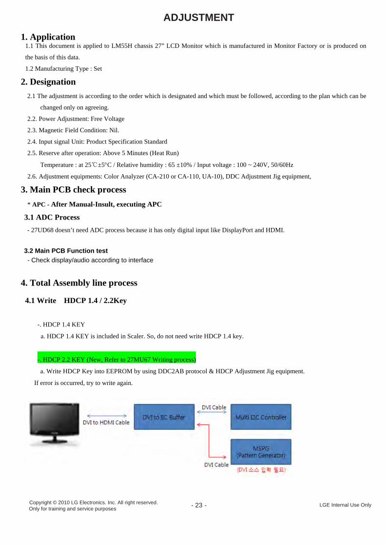
4.1 Write HDCP 1.4 / 2.2Key
-. HDCP 1.4 KEY
a. HDCP 1.4 KEY is included in Scaler. So, do not need write HDCP 1.4 key.
-. HDCP 2.2 KEY (New, Refer to 27MU67 Writing process)
a. Write HDCP Key into EEPROM by using DDC2AB protocol & HDCP Adjustment Jig equipment.
If error is occurred, try to write again.

Copyright © 2010 LG Electronics. Inc. All right reserved. - 24 - LGE Internal Use OnlyOnly for training and service purposes
b. Write HDCP2.2 Key with IIC protocol.
c. Verification method :
Check OSD with aging on mode or using Master Signal generator with HDCP On and connect to Monitor with HDMI
4.2 White balance check and Factory calibration -. Before the factory calibration, check the White balance according to below specification.
HDMI 1920x1080, Full White
Tolerance : -/+0.015 / Luminance Spec(min) : 250
Check condition : custom mode(out-going condition)
Aging Time [min] x y
0~10 0.316 0.335
10~30 0.313 0.332
30~ 0.313 0.329
a. Factory Calibration : Gamma, dE, Color Temperature(6500k)
- Reference Model : 27MU67
- Input : HDMI1/2 , Gray Pattern with Gamma correction using command using “Adjustment Command”
Gamma calibration and verify
*Note : Manual W/B process
1) When in DC OFF Condition
2) and push the Menu Button and On Button at the same time for about 3 secoemd

- 25 -Copyright © 2010 LG Electronics. Inc. All right reserved.Only for training and service purposes
LGE Internal Use Only
3) In Service Menu.
※ When doing Adjustment, Please make circumstance as below.
4.3 DPM Operation check ■ Measurement Condition: 100~240V@ 50/60Hz 1) Set Input to DisplayPort/MiniDP, HDMI1, HDMI2 2) Turn off the source device.
3) Check DPM operation refer to the below table.
Operating Condition Sync (H/V)
or Video
EUT
(MSPG6100)LED(SET) Wattage(W)
Sleep mode Off/Off Off White blinking 0.5W
Off mode - - Off Mech. Switch off
Off 0.3W DC Switch Off
5. Shipping condition
No. Item Content& Outgoing Condition 비고
2 Outgoing Condition
SOURCE HDMI1
Power S/W OFF Brightness 100
OSD Menu
Contrast 70
Volume 30

- 26 -Copyright © 2010 LG Electronics. Inc. All right reserved.Only for training and service purposes
LGE Internal Use Only
Operating. Time
Input HDMI1 *Input Save ad last condition Ratio Wide PBP Off Picture Mode Custom Black Stabilizer 50 Super Resolution+ Off Sharpness 50
Black Level Depends on video signal - Low : RGB limit / YUV - High : RGB Full
Black level enable at HDMI input
UHD Deep Color Off DFC Off Response Time Middle Gamma 2.2 Color Temp Custom (Manual:6500K) Red 50 Green 50 Blue 50
Six Color Hue : 50 Saturation : 50
Language Depend on the sale region Super Energy Saving Low DAS Mode On Power LED Off Automatic Standby Europe : 4H, Others: OFF DisplayPort 1.2 Enable OSD Lock Off Operating Time Within 2Hours
Make sure to do FACTORY RESET at the final process.
- 27 -Copyright © 2010 LG Electronics. Inc. All right reserved.Only for training and service purposes
LGE Internal Use Only
6. Signal composition for adjustment
6.1 I2C (100K BPS) 6.2 COMMUNICATION START
#Until ACK BIT goes LOW, Repeat it. 6.3 Command form.
Command form use DDC2AB standard communication protocol. START 6E A 50 A LEN A 03 A CMD A 00 A VAL A CS A STOP
a. LEN : DATA BYTE number to send.
b. CMD : Command language that monitor executes.
c. VAL : FOS DATA
d. CS : Dada’s CHECHSUM that transmit
e. DELAY : 50MS
f. A : Acknowledge
6.4 Screen adjust command (LENGTH = 84)
No. Adjustment contents CMD(hex
) ADR VAL(hex) Explanation
1 EEPROM ALL INITIAL E4 00 00 adjustment Initialization 2 EEPROM READ E7 Slave
add At EEPROM Read
3 EEPROM WRITE E8 Slave add
Data Write data at EEPROM
4 R GAIN 16 00 00-64 Tune Gain 5 G GAIN 18 00 00-64
6 B GAIN 1A 00 00-64 7 BRIGHT(Backlight) 10 00 00-64 Tune Analog Bright 8 FACTORY RESET F0 00 00 Factory reset 9 AUTO_COLOR_ADJUST F1 00 0 AUTO COLOR Tuning
0:Auto color
10 COLOR_MODE_CHANGE F2 00
01 6500K 02 9300K
11 Elapsed time Clear E9 00 00 Aging off &Clear elapsed time
12 Aging On/Off F3 00 FF/00 FF:ON / 00:OFF
13 Input Select F4 00 0xD0 0x90 0x91
1:DisplayPort 2:HDMI1 3:HDMI2
14 SYSTEM RESET F5 00 00 Restart System
15 Select Language 68 00 0x00 ~
0x0F
00:English,
01: German
02: French
START 6E A STOP 50Ms

- 28 -Copyright © 2010 LG Electronics. Inc. All right reserved.Only for training and service purposes
LGE Internal Use Only
03: Spanish
04: Italian
05: Swedish,
06:Finnish
07: Portuguese
08: Brazil
09: Polish
0A: Russian
0B: Greek
0C: Ukrainian
0D: Chinese
0E:Japanese
0F: Korean
EDID SN UPDATE 0x77 0 0x01~0x020x01 : HDMI1
0x02 : HDMI2
6.5. EEPROM Data Write
6.5.1 Siganl TABLE
LEN : 84h+Bytes
CMD : E8h
ADH : E2PROM Slave Address(A0,A2,A4,A6,A8,AA,AC,AE), Not 00h(Reserved by Buffer To EEPROM)
ADL : E2PROM Sub Address(00~FF)
Data : Write data
Delay : 20ms
6.5.2. Command Set
No. Adjustment contents CMD(hex) LEN Explanation
1 EEPROM WRITE E8 94 16-Byte Write
2 (84+n) n-byte Write
* Use FOS Default write :
<14mode data> write
SyncFlags,HPeriodH, HPeriodL, VtotalH,VtotalL, SrcHTotalH, SrcHTotalL
SrcHStartH, SrcHStartL, SrcVStartH,SrcVStartL, HsyncPhase Temporary Data write: Write to particular address of EEPROM.
STOP
AAA AA 50 6E 03 CMD ADH84+n START ADL A
CS
A
AData_1 A . . . Data_n A Delay 20m

- 29 -Copyright © 2010 LG Electronics. Inc. All right reserved.Only for training and service purposes
LGE Internal Use Only
6.6 E2PROM Data Read
6.6.1 Signal TABLE
----------------------------------------------------------------------
128 Bytes
6.6.2 COMMAND SET
No. Adjustment contents CMD(hex
)
ADH(hex) ADL(hex) Explanation
1 EEPROM READ E7 A0 0 0-Page 0~7F Read
2 80 0-Page 80~FF Read
3 A2 0 1-Page 0~7F Read
4 80 1-Page 80~FF Read
5 A4 0 2-Page 0~7F Read
6 80 2-Page 80~FF Read
7 A6 0 3-Page 0~7F Read
8 80 3-Page 80~FF Read
9 A8 0 4-Page 0~7F Read
10 80 4-Page 80~FF Read
11 AA 0 5-Page 0~7F Read
12 80 5-Page 80~FF Read
13 AC 0 6-Page 0~7F Read
14 80 6-Page 80~FF Read
15 AE 0 7-Page 0~7F Read
16 80 7-Page 80~FF Read
6.6.3 Use Read E2PROM’s specific area as unit of 128(80h)-byte. ( 84h )
6.6.4 EDID Write
EEPROM access by using DDC2B protocol 1-Byte write
L : 0x00~0x7F
D : data 8-byte write
L : 0x00,0x10,….0x70
STOPA A D1 6F
STOP
START
A
A
A
Dn
A A A 50 6E 03 CMD ADH84 START A A ADL A CS
Delay 150ms
STOP
STOPAAA
A
A
L
L
A0
A0 …. Data8
D
Data1
START
START A
A A
- 30 -Copyright © 2010 LG Electronics. Inc. All right reserved.Only for training and service purposes
LGE Internal Use Only
6.6.5 EDID Read
DDC2B Command.(A0/A1)
- 128 Byte transfer of EDID Buffer of MICOM
STOPA 00A0START A A CS A Data1A1START . . . Data128

BLOCK DIAGRAM (Main)
- 31 -Copyright © 2010 LG Electronics. Inc. All right reserved.Only for training and service purposes
LGE Internal Use Only

TROUBLESHOOTING GUIDE
-32 -Copyright © 2010 LG Electronics. Inc. All right reserved.Only for training and service purposes
LGE Internal Use Only
1. NO POWER
`
No power issue
Check JK400 PIN 4
Is IC401 PIN2(19V),PIN
3(5V)
CHECK ADAPTER
CHECK IC401
Is IC 400 PIN2(3.3V) CHECK IC400
Is IC200 PIN95,PIN96
PULSECHECK CRYSTAL X200
YES
YES
YES
NO
NO
NO
NO
CHECK IC200
IC401-#2 IC401-#3 IC400 X200

-33 -Copyright © 2010 LG Electronics. Inc. All right reserved.Only for training and service purposes
LGE Internal Use Only
2. NO RASTER (OSD IS NOT DISPLAYED) – MAIN
No Raster(OSD is not displayed)
Check P201 PIN1(10V)
IC200 PIN95,96 12MHz
CHECK IC402 PIN3(10V)
1.CHECK 2002. Trouble in IC200
Is IC200 PIN3 PIN4 I2C
YES
YES
NO
NO
NO
Trouble in cable or LCD module
CHECK CONNECTION From HDMI TO IC200

-34 -Copyright © 2010 LG Electronics. Inc. All right reserved.Only for training and service purposes
LGE Internal Use Only
3. Trouble in DPM
CHECK Signal cable connection
Trouble in DPM
Check Signal cable DET pin
CHECK PC. PC is going to the DPM mode
YES
YES
NO
NO
Trouble in IC200
Check the Signal input

LGE Internal Use OnlyCopyright © LG Electronics. Inc. All rights reserved.Only for training and service purposes
EXPLODED VIEW
Many electrical and mechanical parts in this chassis have special safety-related characteristics. These parts are identified by in the Schematic Diagram and EXPLODED VIEW. It is essential that these special safety parts should be replaced with the same components as recommended in this manual to prevent X-RADIATION, Shock, Fire, or other Hazards. Do not modify the original design without permission of manufacturer.
IMPORTANT SAFETY NOTICE
910
900
400
300
200
700
520
510
540
930
310

THERMAL
THERMAL
THE SYMBOL MARK OF THIS SCHEMETIC DIAGRAM INCORPORATESSPECIAL FEATURES IMPORTANT FOR PROTECTION FROM X-RADIATION.FIRE AND ELECTRICAL SHOCK HAZARDS, WHEN SERVICING IF IS ESSENTIAL THAT ONLY MANUFACTURES SPECIFIED PARTS BE USED FORTHE CRITICAL COMPONENTS IN THE SYMBOL MARK OF THE SCHEMETIC.
C1000.1uF16V
R103
0
R102
0
HDMI2_5V
R1040
OPT
HDMI2_SDA
HDMI2_DET
HDMI2_HPD
HDMI2_SCL
C102
0.1uF
16V
R111 1K
OPT
R1070
HDMI2_RX2+
+3.3V_NORMAL
HDMI2_RX2-
HDMI2_RX1+
HDMI2_RX1-
HDMI2_RX0+
HDMI2_RX0-
HDMI2_RXC+
HDMI2_RXC-
R1010
OPT
R108
10K
+3.3V_NORMAL
R105
100K
R106 10
+3.3V_NORMAL
R115
10K
C1010.1uF16V
+3.3V_NORMAL
R1100
R109 1K
OPT
R114
10K
HDMI1_RX2-
HDMI1_SDA
HDMI1_DET
HDMI1_HPD
HDMI1_RX1+
HDMI1_5V
HDMI1_RX2+
HDMI1_RX0+
HDMI1_RX0-
R1000
OPT
HDMI1_SCL
HDMI1_RXC+
HDMI1_RX1-
HDMI1_RXC-
R113
1M
R13110
+3.3V_NORMAL
R112
1M
DP_RX_SDM
AR1035.1
AR1045.1
AR1005.1
AR1015.1
C1040.1uF16V
C1030.1uF16V
DP0_RX2P
R119
100K
DP0_RX2NDP0_RX3P
R123
100K
R127
100K
DP0_RX0P
DP0_RX3N
R117
100K
DP0_RX0N
R116
100K
R124
100K
DP0_RX1P
R118
100K
R126
100K
DP0_RX1N
HDMI2_SDA
HDMI_RXC+
HDMI2_RX1-
HDMI_RX1+
HDMI2_RX2+
IC101TS3DV642A0RUAR
1VCC
2EN
3SCL
4SDA
5D0+
6D0-
7D1+
8D1-
9NC_1
10
D2+
11
D2-
12
D3+
13
D3-
14
HPD
15
CEC
16
SEL1
17
SEL2
18CEC_A
19HPD_A
20CEC_B
21HPD_B
22
D3-B
23
D3+B
24
D2-B
25
D2+B
26
B1-B
27
B1+B
28
D0-B
29
D0+B
30
NC_2
31
D3-A
32
D3+A
33
D2-A
34
D2+A
35
D1-A
36
D1+A
37
D0-A
38
D0+A
39 SDA_B40 SCL_B41 SDA_A42 SCL_A
43
[EP]GND
HDMI1_RXC-
HDMI2_SCL
HDMI_SCL
HDMI2_RX0+
R1294.7K
HDMI2_RXC+
HDMI_RXC-
HDMI1_RX1+
+3.3V_NORMAL
HDMI1_RX2+
HDMI_RX1-
HDMI1_HPD
R1214.7K
HDMI2_RX2-
HDMI_RX0+
HDMI1_RXC+
C1060.1uF16V
HDMI1_RX2-
HDMI_SELECTION
HDMI2_HPD
HDMI1_SCL
HDMI2_RXC-
HDMI_RX2+
HDMI1_RX1-
R1254.7K
HDMI1_RX0-
HDMI_RX2-
HDMI1_SDA
HDMI_SDA
HDMI2_RX1+
HDMI2_RX0-
HDMI1_RX0+
HDMI_RX0-
JK100
51V019S-35SN-CR2-B-LG
14NC
13CEC
5DATA1_SHIELD
20
SHIELD
12CLK-
11CLK_SHIELD
2DATA2_SHIELD
19HPD
18+5V_POWER
10CLK+
4DATA1+
1DATA2+
17DDC/CEC_GND
9DATA0-
8DATA0_SHIELD
3DATA2-
16SDA
7DATA0+
6DATA1-
15SCL
JK101
51V019S-35SN-CR2-B-LG
14NC
13CEC
5DATA1_SHIELD
20
SHIELD
12CLK-
11CLK_SHIELD
2DATA2_SHIELD
19HPD
18+5V_POWER
10CLK+
4DATA1+
1DATA2+
17DDC/CEC_GND
9DATA0-
8DATA0_SHIELD
3DATA2-
16SDA
7DATA0+
6DATA1-
15SCL
JK102
62L020S-34A1N-7T0201-HF_
1414
1313
55
1212
1111
22
1919
1818
1010
44
11
1717
99
88
33
1616
77
66
1515
2020
21
21
AR10233
AR10533
DP_DET
HDMI_HPD
VA10010pF18V
VA10210pF18V
VA10410pF18V
VA10710pF18V
VA10910pF18V
VA10110pF18V
VA10310pF18V
VA10510pF18V
VA10810pF18V
VA11010pF18V
VA10610pF18V
DP0_HPD
DP0_RX3N
DP0_RX1N
DP0_RX2N
DP0_RX3P
DP0_RX1P
DP0_RX0P
DP0_RX0N
DP0_RX2P
DP0_AUXN
DP0_AUXP
D100
100VSK510B_TSC
R14324K1%
R1322K1%
OPT
R155
100K
C3404700pF50V
OPT
R138100K
R1521.5K
C1240.47uF16V
R1304.7K1%
WLED_ADIM
R14739KA_DIM
JP106
R136100
C3314.7uF25VIC102
DT1643S
3EN
2VREF1
4PDIM
1VIN
6LS1
5RISET
7LS2
8LGND
9LS3
10LS4
11OVP
12RT
13COMP
14CS
15NDRV
16VREF2
17
[EP]GND
JP104 JP107 JP108
C1251uF50V
C3334.7uF25V
C34333uF100V
WLED_ENABLE
C34433uF100V
R12010K
OPT
R1331K
JP105
+19V
R156100K
P100
12507WR-06L
123456
7
R139100K
A_DIM
+5V_STANDBY
L130
UBW2012-121F
LED_DRIVER_BEAD
Q1002N3904S
E
B
CR1224.7K
R1491.5K
C3391uF50V
C3371000pF50V
+5V_STANDBY
Q102AOD2922
G
D
S
C3221000pF50V
R1281K1%
C3271uF50V
R1610.0751W1%
L13233uH
C1051uF10V
C1261uF50V
+3.3V_HP
C32510pF50V
C33010pF50V
R15310K
C1131uF10V
HP_MUTE
C34610uF10V
C3320.1uF16V
R1424.7K
HP_LOUT
VR101OPT
10pF18V
C1181uF10V
HP_LOUT
+3.3V_HP
HP_ROUT
C3241uF10V
JP102
JP100
C3411uF10V
R1504.7K
+3.3V_HP
R1544.7K
OPT
HP_ROUT_MAIN
R14843K1%
C323180pF50V
C33810uF10V
JK103
PEJ027-03
6B T_TERMINAL2
7B B_TERMINAL2
5 T_SPRING
4 R_SPRING
7A B_TERMINAL1
6A T_TERMINAL1
3 E_SPRING
VR102OPT
10pF18V
JP103
JP101
Q103AO3435
G
DS
VR100OPT
10pF18V
HP_DET
+3.3V_NORMAL
C3201uF10V
C1322.2uF10V
IC100TPA6138A2
3OUTR
2-INR
4GND_1
1+INR
6VSS
5MUTE
7CN
8CP
9VDD
10GND_2
11UVP
12OUTL
13-INL
14+INL
R13510K
Q1012N3904S
E
B
C
HP_ROUT
R15710K
C3291uF10V
R1630
OPT
HP_LOUT_MAIN
R14610K
OPT
HP_OFF
R1451K
R14143K1%
C1351uF10V
OPT
C121180pF50V
+3.3V_NORMAL +3.3V_HP
R1711K
R173100
R17210
C3472200pF50V
R176100
R17510
C3482200pF50V
R1741K
HDMI1_5V
+5V_STANDBY
R158 0OPT
D101BAT54C_TSC
A2
C
A1
AR1064.7K
AR1074.7K
D102BAT54C_TSC
A2C
A1
R164 0OPT
HDMI2_5V
+5V_STANDBY
JP112
JP113
JP114
JP109
JP110
JP111
L131120-ohmBLM15PX121SN1
R1651K
R134100K1%
R1443.9K1%
L130-*10
LED_DRIVER_Oohm
R15120K
R14020K
R13710K
R15924K5%
R16068K
5%
R162470K5%
C1191uF50V
C3281uF50V
C3210.1uF16V
ML_LANE_3-
AUX_CH-
ML_LANE_3+
ML_LANE_1-
ML_LANE_0+
CONFIG2
HOT_PLUG
GND_4
CONFIG1
GND_2
GND_1
RETURN
DP_PWR[3.3V]
ML_LANE_2+
ML_LANE_1+
GND_0
GND_3
ML_LANE_0-
AUX_CH+
ML_LANE_2-
DP
HDMI1
(HDMI2.0)
(HDMI2.0)
DISPLAY PORT
PORT NO.:HDMI1
PORT NO.:HDMI2
This GND Pattern should be very thick
This GND Pattern should be very narrow
This GND Pattern should be very narrow
This GND Pattern should be very thick
For MAC mini DP issue
HDMI2.0 SWITCH
Interface 1 4
27MU68 2015.06.23
(Straight)
HDMI2(Straight)
H H => HDMI 1H L => HDMI 2
SEL1 SEL2
(Straight)
Left Bar(BOTTOM)
20150629110mA setting
LED Driver
Close to IC
2015.01.19OCP 3A->4A
��綫
HPAMP_3.3V_Switch
H/P OUT
Headphone AMP
R134//R143,R144set the Backlight current
20150629 ADD PULL-UP R
20150629 ADD PULL-UP R
20150629 ADD JIG POINT
20150629 ADD JIG POINT
201506291608/2A->1005/2A
20150629 APPLY->OPT
20150629 ADD 1K-R
20150629110mA setting
20150629For reducing power consumption@ DC off
2015063020150630
20150630
201507031 -> 5%

THERMAL
THE SYMBOL MARK OF THIS SCHEMETIC DIAGRAM INCORPORATESSPECIAL FEATURES IMPORTANT FOR PROTECTION FROM X-RADIATION.FIRE AND ELECTRICAL SHOCK HAZARDS, WHEN SERVICING IF IS ESSENTIAL THAT ONLY MANUFACTURES SPECIFIED PARTS BE USED FORTHE CRITICAL COMPONENTS IN THE SYMBOL MARK OF THE SCHEMETIC.
+1.15V_VDD_DDR_B
SYS_EEPROM_SCL
C282 0.1uF 16V
SYS_EEPROM_WP
EDP2-
R260
10K
IC200
MST9U11Q1(UHD Scaler)
1GPIO_X10/CD_SENSE1/SAR10
2GPIO_X11/CABLE5V1
3GPIO_X13/DDCD3_CK/RS232_RX
4GPIO_X14/DDCD3_DA/RS232_TX
5VDDP_1
6GND_1
7VDD_1
8GPIO_X12/HPD1/CBUS1
9HRX0_CN
10HRX0_CP
11AVDD_HRX0
12HRX0_0N
13HRX0_0P
14GND_2
15HRX0_1N
16HRX0_1P
17AVDDL_HRX0_1
18AVDDL_HRX0_2
19HRX0_2N
20HRX0_2P
21GND_3
22AVDD_DP
23DP_RX0P
24DP_RX0N
25GND_4
26DP_RX1P
27DP_RX1N
28AVDDL_DP
29DP_RX2P
30DP_RX2N
31GND_5
32DP_RX3P
33DP_RX3N
34AUXN
35AUXP
36NC_1
37NC_2
38NC_3
39VDD_2
40GND_6
41GND_7
42GND_8
43AVDD_ADC
44BIN0M
45BIN0P
46GIN0M
47GIN0P
48SOGIN0
49RIN0M
50RIN0P
51HSYNC0
52VSYNC0
53AVDD_AUDIO_1
54LINEIN_L0
55LINEIN_R0
56VRM_ADC
57VAG
58LINEOUT_L0
59LINEOUT_R0
60GND_9
61EAROUT_L
62EAROUT_R
63AVDD_AUDIO_2
64GPIO_A8/SPDIFO
65
GPIO_A7/AUMCK
66
GPIO_A6/AUWS
67
GPIO_A2/AUSD0
68
GPIO_A1/AUBCK
69
GPIO_A0/AUMUTE
70
GPIO40/DDCA_CK/RS232_RX
71
GPIO41/DDCA_DA/RS232_TX
72
GPIO42/PWM6
73
GPIO43/PWM7
74
GPIO44/PWM8
75
GPIO45/PWM9
76
GND_10
77
RESET
78
GND_11
79
VDD_NODIE_1
80
VDDP_2
81
CSZ
82
SDO
83
SDI
84
SCK
85
WP/GPIO10
86
/HOLD/GPIO11
87
GPIO00/MSCL0
88
GPIO01/MSDA0
89
GPIO02/PWM0/RS232_TX
90
GPIO03/PWM1/RS232_RX
91
GPIO04/MSCL0/PASS_SCL
92
GPIO05/MSDA0/PASS_SDA
93
GPIO06/PWM4
94
GND_12
95
XOUT
96
XIN
97
AVDD_PLL_1
98
GND_13
99
VDD_3
100
CID
101
VBUS
102
AVDD_USB
103
GND_14
104
USB_DM
105
USB_DP
106
DVDD_DDR_A
107
DVDD_DDR_RX_A
108
AVDD_PLL_2
109
VDDIO_A_1
110
VDDIO_A_2
111
VDD_4
112
VDDIO_A_3
113
VDD_DRAM_A_1
114
VDD_DRAM_A_2
115
VDD_DRAM_A_3
116
VDD_5
117
GND_15
118
AVDDL_PREDRV_1
119
GND_16
120
AVDDL_MOD_1
121
NC_4
122
NC_5
123
NC_6
124
NC_7
125
AVDD_MOD_1
126
GND_17
127
NC_8
128
NC_9
129 NC_10130 NC_11131 NC_12132 NC_13133 NC_14134 NC_15135 AVDD_MOD_2136 AVDDL_PREDRV_2137 GND_18138 AVDDL_MOD_2139 NC_16140 NC_17141 NC_18142 NC_19143 NC_20144 NC_21145 NC_22146 NC_23147 NC_24148 NC_25149 NC_26150 NC_27151 VDD_6152 AVDD_LPLL153 GND_19154 eDP_HBR2_3-155 eDP_HBR2_3+156 eDP_HBR2_2-157 eDP_HBR2_2+158 eDP_HBR2_1-159 eDP_HBR2_1+160 eDP_HBR2_0-161 eDP_HBR2_0+162 NC_40163 NC_41164 NC_42165 NC_43166 GND_20167 AVDDL_MOD_3168 GND_21169 AVDDL_PREDRV_3170 AVDD_MOD_3171 NC_28172 NC_29173 NC_30174 NC_31175 NC_32176 NC_33177 NC_34178 NC_35179 NC_36180 NC_37181 NC_38182 NC_39183 VDD_7184 AUXTXN0185 AUXTXP0186 AUXTXN1187 AUXTXP1188 AUXTXN2189 AUXTXP2190 AUXTXN3191 AUXTXP3192 VDDP_31
93
VDD_NODIE_2
194
eDP_HPD[0]
195
eDP_HPD[1]
196
eDP_HPD[2]
197
eDP_HPD[3]
198
GPIO54/PWM0/EXTINT0
199
GPIO55/PWM1/EXTINT1
200
GPIO56/PWM8/EXTINT2
201
GPIO57/PWM9/EXTINT3
202
GND_22
203
VDDP_4
204
GPIO20/PWM2
205
GPIO21/PWM3
206
GPIO22/PWM4/SAR4
207
GPIO23/PWM5/SAR5
208
GPIO24/CEC3/PWM6
209
GPIO25/CEC2/PWM7
210
GPIO26/CEC
211
GPIO27/IR
212
SAR0/GPIO_SAR0
213
SAR1/GPIO_SAR1
214
SAR2/GPIO_SAR2
215
SAR3/GPIO_SAR3
216
VDD_8
217
DVDD_DDR_B
218
DVDD_DDR_RX_B
219
AVDD_PLL_3
220
VDDIO_B_1
221
VDDIO_B_2
222
VDD_9
223
VDDIO_B_3
224
VDD_DRAM_B_1
225
VDD_DRAM_B_2
226
VDD_DRAM_B_3
227
GPIO_X40/CD_SENSE4/SAR7
228
GPIO_X41/CABLE5V4
229
GPIO_X42/HPD4/CBUS4
230
GPIO_X43/RS232_RX/DDCD1_CK
231
GPIO_X44/RS232_TX/DDCD1_DA
232
GPIO_X30/CD_SENSE3/SAR8
233
GPIO_X31/CABLE5V3
234
GPIO_X32/HPD3/CBUS3
235
GPIO_X33/RS232_RX/DDCD0_CK
236
GPIO_X34/RS232_TX/DDCD0_DA
237
VDD_10
238
AVDDL_RX
239
RX1_CN
240
RX1_CP
241
RX1_0N
242
RX1_0P
243
RX1_1N
244
RX1_1P
245
RX1_2N
246
RX1_2P
247
GND_23
248
AVDD_RX
249
RX0_CN
250
RX0_CP
251
RX0_0N
252
RX0_0P
253
RX0_1N
254
RX0_1P
255
RX0_2N
256
RX0_2P
257
[EP]
+1.15V_VDD
C25915pF50V
SDI
C26015pF50V
SDO
R2514.7K
HDMI_SELECTION
AVDD_AUDIO
AVDD_RX
SCK
HDMI_5V
SCK
IC202
MX25L8006EM2I-12G
3WP#
2SO/SIO1
4GND
1CS#
5SI/SIO0
6SCLK
7HOLD#
8VCC
R2214.7K
EDP0+
C2660.1uF16V
HDMI1_5V
C277 0.1uF 16V
CS
Q203AO3435
G
DS
AVDD_MOD
DP0_HPD
Q201AO3435
G
DS
IC201AT24C32D-SSHM-T
3A2
2A1
4GND
1A0
5SDA
6SCL
7WP
8VCC
HDMI1_5V_SEL
AVDDL_MOD
C2670.1uF16V
HDMI2_5V
AVDD_DP
HDMI_5V
EDP1-
R2204.7K
AVDD_ADC
SDO
AVDDL_MOD
HDMI2_5V_SEL
PD_CTL
HOLD
DP0_RX2P
R2184.7K
AVDDL_PREDRV
AVDDL_PREDRV
R2174.7K
VDDP
R26110K
C281 0.1uF 16V
R210
10
+1.15V_VDD
EDP0-
HP_OFF
C279 0.1uF 16V
R232100K
SYS_EEPROM_SCL
R20510K
OPT
KEY1
VDDIO_B
HP_MUTE
+1.15V_VDD
DP0_RX1N
SYS_EEPROM_WP
HP_LOUT_MAIN
HDMI_RXC-
WLED_ENABLE
EDP2+
SYS_EEPROM_SDA
PD_CTL_DDR
VDDP
EDP3+
AVDDL_DP
AVDD_USB
R2150
+3.3V_NORMAL
R244
0R20110K
+3.3V_NORMAL
DP_RX_SDM
R20010K
OPT
AVDD_HRX0
R243
200K
R20710K
R219 10
AR20433
R20210K
AVDD_PLL
AR20133
BOOT4
DP0_RX0N
R242
200K
R25433
R20310K
OPT
+1.15V_VDD
R229 10
AR20233
BOOT3
CS
+1.15V_VDD
BOOT1
R25533
OSCI
HDMI1_DET
AR20310K
BOOT2
AVDDL_PREDRV
HP_DET
R20610K
X20012MHz
R20810K
OPT
DP0_RX3P
HDMI2_5V_SEL
AVDD_MOD
L200
HDMI1_5V_SEL
C278 0.1uF 16V
+1.15V_VDD
DP0_RX1P
C280 0.1uF 16V
HDMI_SCL
HDMI_SDA
AVDDL_MOD
+1.15V_VDD_DDR_A
+1.15V_VDD
R20910
C2051uF10V
+1.15V_VDD
HP_ROUT_MAIN
C2041uF10V
R230
1K
HDMI_RX0+
DP0_RX0P
R231 1K
R224100K
OPT
VDDIO_A
VDDP
AVDD_MOD
Q2002N3904S
E
B
C
HDMI_RX2+
BOOT2
JP201
Q2022N3904S
E
B
C
R223100K
OPT
HDMI_RX2-
EDP_HPD
C26310uF10V
VDD_DRAM_B
IR
OSCO
C2620.1uF16V
OPT
CONTROL_LED
EDP_AUX_CHP
HDMI_RX1-
C2740.1uF16V
EDP_AUX_CHN
+3.3V_NORMAL
OSCO
DP0_RX3N
C29268pF50V
OPT
HDMI_5V
C29368pF50V
OPT
C283 0.1uF 16V
C29068pF50V
OPT
R26510
C2750.1uF16V
C29168pF50V
OPT
WP_SPI
R246 10
DP0_AUXN
R245 10
VDD_DRAM_A
EDP0+
HDMI2_DET
EDP2-
HOLD
EDP2+
R23433
SDI
EDP_AUX_CHN
AVDDL_HRX0
EDP1-
C2020.47uF16V
AVDD_PLL
EDP1+
EDP0-
EDP_HPD
C2384.7uF25V
OPT
C276 0.1uF 16V
EDP3-
KEY2
PANEL_ON
HDMI_RX0-
+10V_PANEL
C20310uF10V
OPT
HDMI_RX1+
EDP_AUX_CHP
HDMI_HPD
R26610K
+5V_STANDBY
HDMI_RXC+
EDP1+
EDP3-
EDP3+
DP0_RX2N
C2294.7uF25V
R23310K
DP0_AUXP
OSCI
BOOT3
BOOT1
R22247K
BOOT4
VDDP
WP_SPI
AVDDL_RX
SYS_EEPROM_SDA
+3.3V_NORMAL
+3.3V_NORMAL
+3.3V_NORMAL
C29410uF10V
5V_ST_ON
WLED_ADIM
DP_DETR211 1KR241
10
+3.3V_NORMAL
R23810K
OPT
10KR239
JP203
R2143.3K
L201
BLM15PX121SN1
WHITE LED OPT
R227
4.7K
VR202
18V10pF
R2264.7K
OPT
R22510
P200
12507WR-08L
1
2
3
4
5
6
7
8
9
R2133.3K
Q2042N3904S
E
B
C
R2284.7K
OPT
L202BLM15PX121SN1RED LED OPT
ZD2005.6V
IR
JP204
KEY2
C20168pF50V
OPTJP208
VR201
18V10pF
R204100
IR
JP207
KEY1
+3.3V_NORMAL
+5V_STANDBY
C2001uF10V
JP206
JP205
VR203
18V
OPT
10pF
R21610
CONTROL_LED
P202
12507WS-04L
DE_BUG
1
2
3
4
5
AR20710K
DE_BUG
AR200 33
DE_BUG
R21210
IR
RAC34057401S5
RAC34057401S3
RAC34057401S1
RAC34057401S4
RAC34057401S2
JP200
JP209
R240 0
R235 0
R237 0
R247 0
R248 0
R249 0
R250 0
R236 0
JP210
D200BAT54C
A2
C
A1
HDMI_5V
R2530
OPT
R2520
OPT
C2641000pF50V C265
1000pF50V
BUZZER_PWM
+5V_STANDBY
R25633
R2571K
BU200PKM13EPY-4002-B0
1
2
Q2052N3904S
E
B
C
R2590R258
0OPT
+3.3V_NORMAL
JP202
BUZZER_PWM
P201
05030HR-H30C1(G)
EDP_WAFER
1
2
3
4
5
6
7
8
9
10
11
12
13
14
15
16
17
18
19
20
21
22
23
24
25
26
27
28
29
30
31
2 4Scalar / Key
2015.06.2327MU68
CRYSTAL
Close to IC
SBUS
H
H
GPIO43
GPIO45
L EXT RIU
GPIO44
L
L
H
FUNCTION
H
BOOT-STRAP
GPIO45
H L
GPIO42
L BOOT from R2
L
L
GPIO42
L
L
GPIO43
BOOT from 51
L
H
GPIO44
SYSTEMEEPROM
FLASH MEMORY
SYSTEM EEPROM
FLAH8MBIT
SOLDER PRE-FORM
MODULE-eDPIIC for Debugging(from MP, delete this parts)
20150116 Crystal matching test22pF->15pF
RESET
Close to scalar P79
Close to scalar P193
Angle (8P)
Joystick Key
BEEPUZZER

THE SYMBOL MARK OF THIS SCHEMETIC DIAGRAM INCORPORATESSPECIAL FEATURES IMPORTANT FOR PROTECTION FROM X-RADIATION.FIRE AND ELECTRICAL SHOCK HAZARDS, WHEN SERVICING IF IS ESSENTIAL THAT ONLY MANUFACTURES SPECIFIED PARTS BE USED FORTHE CRITICAL COMPONENTS IN THE SYMBOL MARK OF THE SCHEMETIC.
C12210uF10V
OPT
+1.15V_VDD
C21610uF10V
C1410.1uF16V
C29710uF10V
C1370.1uF16V
C2370.1uF16V
L104
BLM18PG121SN1D
C11110uF10V
L119
BLM18PG121SN1D
C1470.1uF16V
C2980.1uF16V
C1284.7uF6.3V
OPT
C2430.1uF16V
VDDIO_B
+1.15V_VDD_DDR_A
C2360.1uF16V
C1520.1uF16V
C1380.1uF16V
C21810uF10V
C2070.1uF16V
OPT
C1440.1uF16V
C11010uF10V
C1274.7uF6.3V
OPT
L120
BLM18PG121SN1D
C1970.1uF16V
C1570.1uF16V
AVDD_USB
C10810uF10V
AVDD_AUDIO
L114
BLM18PG121SN1D
AVDDL_PREDRV
AVDDL_DP
C11210uF10V
C22510uF10V
C1620.1uF16V
L102
BLM18PG121SN1D
AVDD_MOD
C17810uF10V
OPT
C1510.1uF16V
C1610.1uF16V
OPT
L100
BLM18PG121SN1D
C2530.1uF16V
OPT
VDD_DRAM_B
C1640.1uF16V
AVDDL_RX
C22810uF10V
C1990.1uF16V
C1560.1uF16V
C21710uF10V
OPT
L112
BLM18PG121SN1D
C1670.1uF16V
L123
BLM18PG121SN1D
C18410uF10V
C1550.1uF16V
OPT
L101
BLM18PG121SN1D
C18210uF10V
OPT
C1690.1uF16V
C21910uF10V
OPT
C1940.1uF16V
C1310.1uF16V
C1360.1uF16V
AVDD_ADC
C17610uF10V
C1530.1uF16V
OPT
C2460.1uF16V
AVDD_HRX0
L108
BLM18PG121SN1D
C1920.1uF16V
C1740.1uF16V
OPT
C1291uF10V
OPT
L118
BLM18PG121SN1D
C11610uF10V
C21310uF10V
C2390.1uF16V
C17710uF10V
C1890.1uF16V
OPT
C2500.1uF16V
C21510uF10V
OPT
C2330.1uF16V
C2300.1uF16V
C1980.1uF16V
C1790.1uF16V
OPT
L103
BLM18PG121SN1D
C2400.1uF16V
AVDD_RX
C22310uF10V
C1660.1uF16V
OPT
L116
BLM18PG121SN1D
C1930.1uF16V
C1850.1uF16V
OPT
AVDDL_HRX0
C2310.1uF16V
C21410uF10V
OPT
C2340.1uF16V
VDDP
C2080.1uF16V
L107
BLM18PG121SN1D
C2420.1uF16V
L111
BLM18PG121SN1D
+3.3V_NORMAL
C22010uF10V
VDDIO_A
C11510uF10V
C1390.1uF16V
L117
BLM18PG121SN1D
C2510.1uF16V
OPT
AVDD_PLL
L121
BLM18PG121SN1D
L113
BLM18PG121SN1D
AVDDL_MOD
C12010uF10V
C22210uF10V
C22410uF10V
OPT
C17510uF10V
C2490.1uF16V
C18310uF10V
OPT
C1480.1uF16V
C10910uF10V
OPT
C2570.1uF16V
OPT
C2350.1uF16V
VDD_DRAM_A
C11410uF10V
C2410.1uF16V
C1540.1uF16V
OPT
C2520.1uF16V
OPT
C18110uF10V
OPT
+1.15V_VDD
C2450.1uF16V
C1340.1uF16V
C1300.1uF16V
C1910.1uF16V
C12310uF10V
C2060.1uF16V
OPT
C1600.1uF16V
OPT
+1.8V_DDR
C1960.1uF16V
C1330.1uF16V
L122
BLM18PG121SN1D
C1420.1uF16V
+1.15V_VDD_DDR_B
C2321uF10V
AVDD_DP
C1700.1uF16V
L124
BLM18PG121SN1D
C22710uF10V
OPT
C2090.1uF16V
C1630.1uF16V
OPT
C2481uF10V
C2551uF10V
C2261uF10V
C1171uF10V
C1880.1uF16V
C1870.1uF16V
C107100uF16V
OPT
MAIN IC-CAP
close to Q1
Reserved on Botton side
Reserved on Botton side
close to Q1
close to Q1
Reserved on Botton side
close to Q1
close to Q1
close to Q1
close to Q1
close to Q1
close to Q1
Place Cap on Botton side
close to Q1
close to Q1
Place Cap on Botton side
Reserved on Botton side
close to Q1
Reserved on Botton sideclose to Q1
close to Q1
MAIN IC POWER LINE - CAPACITOR
Reserved on Botton side
Far away AVDDL_PREDRV
Reserved on Q1 bottom layer.pin99/pin116/pin7/pin216
close to Q1Reserved on Q1 bottom layer.pin167
close to Q1Reserved on Q1 bottom layer.pin169
20141028
Far away +1.15V_VDD bypass capclose to s.w. power
close to Q1
close to Q1
Place Cap on Botton side
close to Q1
close to Q1
-> 23mA
-> 23mA
-> 38mA
-> 75.2mA
-> 1291mA
-> 4.6mA
-> 11.7mA
-> 26mA
-> 115.6mA
-> 135.4mA
-> 46.8mA
-> 49.1mA
-> 25.6mA
-> 5.8mA
-> 8.8mA
-> 76.4mA
-> 174.6mA
-> 173.6mA
-> 100.5mA
-> 99.8mA
27MU68 2014.06.23
43
-> 159mA
20150709

THE SYMBOL MARK OF THIS SCHEMETIC DIAGRAM INCORPORATESSPECIAL FEATURES IMPORTANT FOR PROTECTION FROM X-RADIATION.FIRE AND ELECTRICAL SHOCK HAZARDS, WHEN SERVICING IF IS ESSENTIAL THAT ONLY MANUFACTURES SPECIFIED PARTS BE USED FORTHE CRITICAL COMPONENTS IN THE SYMBOL MARK OF THE SCHEMETIC.
PANEL_ON
C4180.1uF16V
+10V_PANEL
C4150.1uF50V
R4132K
OPT
R40147K
IC402MP2315GJ
3SW
2IN
4GND
1AAM
5BST
6EN/SYNC
7VCC
8FB
R40047K
C4120.1uF50V
IC400MP2315GJ
3SW
2IN
4GND
1AAM
5BST
6EN/SYNC
7VCC
8FB
C4160.1uF16V
C4190.1uF16V
+3.3V_NORMAL
+5V_STANDBY
C4070.1uF50V
C4060.1uF50V
C4200.1uF50V
+19V R405100
C42510uF10V
C42210uF10V
C4140.1uF16V
OPT
C4044.7uF25V
OPT
C4014.7uF25V
OPTC4034.7uF25V
JP403
JP402
JP404
JP405
JP401
JP400
C4090.1uF50V
C41068uF35V
+19V
C4284.7uF25V
OPTC4244.7uF25V
C4274.7uF25V
R406100
R408100
ZD4005VR415
51K
R41718K1%
R4185.6K1%
JK400
KJA-DC-1-0032
1 1
2 2
4 4
R421120K1%
+3.3V_NORMAL
R424
10K
Q4032N3904S
E
B
C
Q4012N3904S
E
B
C
R404
10K
R4031K
PD_CTLZ_1.8V
AR40110K
PD_CTL
R4231K
PD_CTL_DDR
AR40010K
Q4022N7002KA G
D
S
PD_CTLZ_1.15V
+3.3V_NORMAL
Q4002N7002KA G
D
S
R40910K
OPT
R42210K1%
R41451K
+5V_STANDBY
C4394.7uF25V
OPT
IC401MP2315GJ
3SW
2IN
4GND
1AAM
5BST
6EN/SYNC
7VCC
8FB
C4410.1uF50V
C4420.1uF50V
R43547K
R44051K
5V_ST_ON
+19V
C4430.1uF16V
R436100
+5V_STANDBY
R439100
C4404.7uF25V
+19V
L401
C4004.7uF25V
L400OPT
R402100K
R437100K
OPT
R43815K
OPT
C44710uF10V
C44810uF10V
C4460.1uF16V
ZD4055.6V
OPT
R44175K1%
R44214K1%
C4110.1uF50V
OPT
C4450.1uF50V
R41015K
R4442K
OPT
R41147K
C4210.1uF50V
OPT
C40210uF10V
R40747K
R416
100
C45510uF10V
C4510.1uF
16V
C4440.1uF16V
PD_CTLZ_1.15V
ZD401
2.5V
R451
3.3K
1%
IC405MP2315GJ
3SW
2IN
4GND
1AAM
5BST
6EN/SYNC
7VCC
8FB
+5V_STANDBY
PD_CTLZ_1.8V
C4500.1uF
16V
C45410uF10V
R419
100
C4170.1uF50V
IC404MP2315GJ
3SW
2IN
4GND
1AAM
5BST
6EN/SYNC
7VCC
8FB
C4230.1uF50V
+1.8V_DDR
C45210uF10V
R443
10K
OPT
C4260.1uF16V
R449
15K
1%
C4130.1uF50V
C4490.1uF16V ZD404
2.5V
C4080.1uF50V
R452
10K
1%
C40510uF10V
C45310uF10V
R412100
R420100
R44551K
R44651K
+1.15V_VDD
L40410uH
L40510uH
L40310uH
L407
4.7uH
L408
4.7uH
R447
10K
1%
R448
10K
1%
R450
1.5K
1%
MAIN POWER
3A
3A
Setting: 10.40V(=0.8(1+120K/10K)
Setting: 3.37V=0.8(1+18K/5.6K)
For Jig Test
DC-JacK (Straight Type)
27MU68 2015.06.23
44
Power sequence Circuit for 1.8V / 1.15V
SCALAR DC-DC BLOCK
3ASetting: 5.06V(=0.8(1+75K/14K)
3A
3A
20150709
20150709


![ERP Rev00 Issue01[1]](https://img.dokumen.tips/doc/110x75/552c56fe4a7959fa7c8b46d9/erp-rev00-issue011.jpg)