Embed Size (px)
Citation preview

© Semiconductor Components Industries, LLC, 2015
August, 2015 − Rev. 11 Publication Order Number:
NLAS54405/D
NLAS54405
Low THD+N Stereo SPDTSwitch with Click and PopElimination
The NLAS54405 is a single supply, bidirectional, dual single−pole /double−throw (SPDT) ultra-low distortion, high OFF−Isolationanalog switch that can pass analog signals that are positive andnegative with respect to ground. It is primarily targeted at consumerand professional audio switching applications such as computer soundcards and home theater products. The inputs can accommodate groundreferenced signals up to 2 VRMS while operating from a single 3.3 V or5 V DC supply. The digital logic inputs are 1.8 V logic−compatiblewhen using a single 3.3 V or 5 V supply. It can be used in both AC− orDC−coupled ground-referenced applications.
The NLAS54405 has a delayed turn−on feature and click/popcircuitry at each signal pin that eliminates clicks and pops associatedwith power−up/down conditions of the preceding amplifier outputs.
With −117 dB THD+N performance with a 2 VRMS signal into20 k� load, superior signal muting, high PSRR and very flatfrequency response, the NLAS54405 meets the exacting requirementsof consumer and professional audio engineers.
Features• Dual SPDT Switch or 2−to−1 MUX
• Clickless Audio Switching
• 2 VRMS Signal Switching from 3.3 V or 5 V Supply
• −117 dB THD+N into 20 k� Load at 2 VRMS
• −106 dB THD+N into 32 � Load at 3.9 mW
• Signal to Noise Ratio: > 119 dBV
• ±0.006 dB Insertion Loss at 1 kHz, 20 k� Load
• ±0.002 dB Gain Variation 20 Hz to 20 kHz
• 107 dB Signal Muting into 20 k� Load
• 125 dB PSRR 20 Hz to 20 kHz
• Single Supply Operation: 3.3 V or 5 V
• 16−Lead WQFN Package, 1.8 mm x 2.6 mm
• This Device is Pb−Free, Halogen Free/BFR Free and is RoHSCompliant
Applications• Computer Sound Cards
• Home Theater Audio Products
• SACD / DVD Audio
• DVD Player Audio Output Switching
• Headsets for MP3 / Cellphone Switching
• Hi−Fi Audio Switching Application
www.onsemi.com
MARKING DIAGRAM
WQFN16MT SUFFIX
CASE 488AP
Device Package Shipping†
ORDERING INFORMATION
NLAS54405MT2TBG WQFN16(Pb−Free)
3000 / Tape& Reel
†For information on tape and reel specifications,including part orientation and tape sizes, pleaserefer to our Tape and Reel Packaging SpecificationBrochure, BRD8011/D.
AH = Specific Device CodeM = Date Code & Assembly Location� = Pb−Free Device
AH M�
1

NLAS54405
www.onsemi.com2
Figure 1. Block Diagram
For 5 V operation, connect the 5 V_Supply pin to 5 V and float the VDD pin. For3.3 V operation, connect the VDD pin to 3.3 V and float the 5 V_Supply pin.
CLICK / POPSUPPRESSION
andLOGIC CONTROL
5V_Supply VDD
L
R
GND
L1
L2
R1
R2
NLAS54405
DIR_SEL
AC/DC
MUTE
SEL
CAP_SS
Table 1. FUNCTION TABLE
Inputs Outputs
AC/DC DIR MUTE SEL L1, R1 L2, R2COM (L, R)
C/P SHUNTSL1, R1
C/P SHUNTSL2, R2
C/P SHUNTS
0 X 0 0 ON OFF OFF OFF OFF
0 X 0 1 OFF ON OFF OFF OFF
0 X 1 X OFF OFF OFF OFF OFF
1 0 0 0 ON OFF OFF OFF ON
1 0 0 1 OFF ON OFF ON OFF
1 0 1 X OFF OFF OFF ON ON
1 1 0 0 ON OFF OFF OFF OFF
1 1 0 1 OFF ON OFF OFF OFF
1 1 1 X OFF OFF ON OFF OFF
NOTE: MUTE, AC/DC, DIR: Logic “0” ≤ 0.5 V, Logic “1” ≥ 1.4 V or float with a 3.3 V supply or 5 V supply.SEL: Logic “0” ≤ 0.5 V, Logic “1” ≥ 1.4 V with a 3.3 V supply or 5 V supply.X = Don’t Care

NLAS54405
www.onsemi.com3
Figure 2. WQFN16 Pinout – Top View
Table 2. PIN DESCRIPTIONS
Pin Name Pin Number Description
VDD 14 System power supply pin (+3 V to +3.6 V) (float pin for 5 V applications)
5V_Supply 15 5 V supply pin (+4.5 V to +5.5 V) (float pin for 3.3 V applications)
GND 5, 7, 8 Ground connection
CAP_SS 13 Delayed turn−on capacitor pin
MUTE 1 Signal mute control pin
SEL 4 Input select control pin
AC/DC 16 AC/DC select control pin
DIR_SEL 6 Direction select control pin
R 3 Analog switch common pin for Right
L 2 Analog switch common pin for Left
R2, L2 9, 11 Analog switch normally open pin
R1, L1 10, 12 Analog switch normally closed pin

NLAS54405
www.onsemi.com4
MAXIMUM RATINGS
Symbol Rating Value Unit
VDD Positive 3 V DC Supply Voltage −0.5 to +4.1 V
5V_Supply Positive 5 V DC Supply Voltage −0.5 to +7.0 V
VIS Analog Input/Output Voltage (L1, L2, R1, R2, L, R) −3.1 to VDD + 0.5 V
VIN Digital Select Input Voltage (SEL, MUTE, AC/DC, DIR_SEL) −0.5 to VDD + 0.5 V
IIO Switch Continuous Current (L1, L2, R1, R2, L, R) ±300 mA
IIO_PK Switch Peak Current (L1, L2, R1, R2, L, R)(Pulsed 1ms, 10% Duty Cycle, Max).
±500 mA
PD Power Dissipation in Still Air 800 mW
TL Lead Temperature, 1 mm from Case for 10 seconds 260 °C
TJ Junction Bias Under Bias 150 °C
�JA Thermal Resistance 80 °C/W
Ts Storage Temperature −65 to +150 °C
MSL Moisture Sensitivity Level 1
FR Flammability Rating Oxygen Index: 30% − 35% UL94−V0 (0.125 in)
ESD ESD Protection Human Body ModelCharged Device Model
> 1000> 2000
V
IL Latch−up Current, Above VCC and below GND at 125°C (Note 1) ±300 mA
Stresses exceeding those listed in the Maximum Ratings table may damage the device. If any of these limits are exceeded, device functionalityshould not be assumed, damage may occur and reliability may be affected.1. Tested to EIA/JESD78.
RECOMMENDED OPERATING CONDITIONS
Symbol Parameter Min Max Unit
VDD Positive 3 V DC Supply Voltage 3.0 3.6 V
5V_Supply Positive 5 V DC Supply Voltage 4.5 5.5 V
VS Switch Input / Output Voltage (L1, L2, R1, R2, L, R) −2.9 VDD V
VIN Digital Select Input Voltage GND VDD V
TA Operating Temperature Range −40 +85 °C
Functional operation above the stresses listed in the Recommended Operating Ranges is not implied. Extended exposure to stresses beyondthe Recommended Operating Ranges limits may affect device reliability.

NLAS54405
www.onsemi.com5
DC ELECTRICAL CHARACTERISTICS (Voltages referenced to GND)3.3 V Supply: VDD = +3.0 V to +3.6 V, GND = 0 V, VDIR_SEL = VAC/DC = GND, V5V_SUPPLY = Float, VSIGNAL = 2 VRMS, RLOAD = 20 k�,f = 1 kHz, VSELH = VMUTEH = 1.4 V, VSELL = VMUTEL = 0.5 V, CAP_SS = 0.1 �F, (Note 2), Unless otherwise specified.
Parameter Test ConditionsSupply
(V)Temp(�C)
Min(Notes 3, 4) Typ
Max(Notes 3, 4) Units
ANALOG SWITCH CHARACTERISTICS
Analog Signal Range,VANALOG
3.3, 5 Full − 2 − VRMS
ON−Resistance, rON VDD = 3.3 V, IR or IL = 80 mA, VLx or VRx 3.3 25 − 2.1 − �
= −2.828 V to +2.828 V (See Figure 6) Full − 2.5 −
rON Matching BetweenChannels, �rON
VDD = 3.3 V, IR or IL = 80 mA, VLx or VRx 3.3 25 − 0.046 − �
= Voltage at max rON over −2.828 V to+2.828 V (Note 7)
Full − 0.23 − �
rON Flatness, rFLAT(ON) VDD = 3.3 V, IR or IL = 80 mA, VLx or VRx 3.3 25 − 0.047 0.05 �
= −2.828 V, 0 V, +2.828 V (Note 5) Full − 0.092 −
L, R, Lx, Rx Pull−downResistance
VDD = 3.6 V, VLx or VRx = −2.83 V, 2.83 V,VL or VR = −2.83 V, 2.83 V, VAC/DC = 0 V,
3.6 25 225 300 375 k�
VMUTE = 3.6 V, measure current, calcu-late resistance.
Full − 345 −
DYNAMIC CHARACTERISTICS
THD+N VSIGNAL = 2 VRMS, f = 1 kHz, A−weight-ed filter, RLOAD = 20 k�
3.3, 5 25 − < −117 − dB
VSIGNAL = 1.9 VRMS, f = 1 kHz,A−weighted filter, RLOAD = 20 k�
25 − < −117 −
VSIGNAL = 1.8 VRMS, f = 1 kHz,A−weighted filter, RLOAD = 20 k�
25 − < −117 −
VSIGNAL = 0.707 VRMS, f = 1 kHz,A−weighted filter, RLOAD = 32 �
25 − < −106 −
SNR f = 20 Hz to 20 kHz, A−weighted filter, in-puts grounded, RLOAD = 20 k� or 32 �
3.3, 5 25 − > 119 − dBV
Insertion Loss, GON f = 1 kHz, RLOAD = 20 k� 3.3 25 − ±0.006 − dB
Gain vs Frequency, Gf f = 20 Hz to 20 kHz, RLOAD = 20 k�, ref-erence to GON at 1 kHz
3.3 25 − ±0.002 − dB
Stereo Channel ImbalanceL1 and R1, L2 and R2
f = 20 Hz to 20 kHz, RLOAD = 20 k� 3.3 25 − ±0.001 − dB
OFF−Isolation (Muting) f = 20 Hz to 22 kHz, L = R = 2 VRMS,RLOAD = 20 k�, MUTE = AC/DC =3.3 V, DIR_SEL = GND, SEL = “X”
3.3, 5 25 − 107 − dB
f = 20 Hz to 22 kHz, L1, R1, L2, R2 =2 VRMS, RLOAD = 20 k�, MUTE = AC/DC= DIR_SEL = 3.3 V, SEL = “X”
25 − 108.8 −
f = 20 Hz to 22 kHz, VL or VR =0.7 VRMS, RLOAD = 32 �
25 − 108.5 −
2. VIN = input voltage to perform proper function.3. The algebraic convention, whereby the most negative value is a minimum and the most positive a maximum, is used in this data sheet.4. Parameters with MIN and/or MAX limits are 100% tested at +25°C, unless otherwise specified. Temperature limits established by charac-
terization and are not production tested.5. Flatness is defined as the difference between maximum and minimum value of ON−resistance at the specified analog signal voltage points.6. Limits established by characterization and are not production tested.7. rON matching between channels is calculated by subtracting the channel with the highest max rON value from the channel with lowest max
rON value.8. Crosstalk is inversely proportional to source impedance.

NLAS54405
www.onsemi.com6
DC ELECTRICAL CHARACTERISTICS (Voltages referenced to GND)3.3 V Supply: VDD = +3.0 V to +3.6 V, GND = 0 V, VDIR_SEL = VAC/DC = GND, V5V_SUPPLY = Float, VSIGNAL = 2 VRMS, RLOAD = 20 k�,f = 1 kHz, VSELH = VMUTEH = 1.4 V, VSELL = VMUTEL = 0.5 V, CAP_SS = 0.1 �F, (Note 2), Unless otherwise specified.
Parameter UnitsMax
(Notes 3, 4)TypMin
(Notes 3, 4)Temp(�C)
Supply(V)Test Conditions
DYNAMIC CHARACTERISTICS
Crosstalk (Channel−to−Channel)
RL = 20 k�, f = 20 Hz to 20 kHz, VSIG-
NAL = 2 VRMS, signal source impedance= 20 �, (Note 8)
3.3 25 − 97 − dB
RL = 32 �, f = 20 Hz to 20 kHz, VSIGNAL= 0.7 VRMS, signal source impedance =20 �, (Note 8)
25 − 108 −
PSRR f = 1 kHz, VSIGNAL= 100 mVRMS, inputsgrounded
3.3, 5 25 − 125 − dB
f = 20 kHz, VSIGNAL= 100 mVRMS, in-puts grounded
25 − 125 −
Bandwidth, −3 dB RLOAD = 50 � 3.3 25 − 450 − MHz
ON to Mute Time, TTRANS−OM
CAP_SS = 0.1 �F 3.3 25 − 250 − ns
Mute to ON Time, TTRANS−MO
CAP_SS = 0.1 �F, RLOAD = 32 �, VIS =1.5 V
3.3 25 − 1680 − �s
Turn−ON Time, tON VDD = 3.3 V, VLx or VRx = 1.5 V, VMUTE =0 V, RL = 32 � (See Figure 3)
3.3 25 − 11 − �s
Turn−OFF Time, tOFF VDD = 3.3 V, VLx or VRx = 1.5 V, VMUTE =0 V, RL = 32 � (See Figure 3)
3.3 25 − 95 − ns
Break−Before−Make TimeDelay, tD
VDD = 3.6 V, VLx or VRx = 1.5 V, VMUTE =0 V, RL = 32 � (See Figure 4)
3.6 25 − 10 − �s
OFF−Isolation RL = 50 �, f = 1 MHz, VL or VR =1 VRMS (See Figure 5)
3.3 25 − 68 − dB
Crosstalk (Channel−to−Channel)
RL = 50 �, f = 1 MHz, VL or VR =1 VRMS (See Figure 7)
3.3 25 − 77 − dB
Lx, Rx OFF Capacitance,COFF
f = 1 MHz, VLx or VRx = VL or VR = 0 V(See Figure 8)
3.3 25 − 3.3 − pF
L, R ON Capacitance,CCOM(ON)
f = 1 MHz, VLx or VRx = VCOM = 0 V(See Figure 8)
3.3 25 − 10.5 − pF
POWER SUPPLY CHARACTERISTICS
Power Supply Range, VDD 5V_Supply = Float 3.3 Full 3 − 3.6 V
Power Supply Range,5V_Supply
VDD = Float 5 Full 4.5 − 5.5 V
Positive SupplyCurrent, I+
VDD = +3.6 V, VMUTE = 0 V, 3.6 25 − 54 65 �A
VSEL = 0 V or VDD Full − 59 − �A
VDD = +3.6 V, VMUTE = VDD, 3.6 25 − 14 20 �A
VSEL = 0 V or VDD Full − 15 − �A
VDD = +3.6 V, VMUTE = 0 V, 3.6 25 − 55 65 �A
VSEL = 1.8 V Full − 58 − �A
2. VIN = input voltage to perform proper function.3. The algebraic convention, whereby the most negative value is a minimum and the most positive a maximum, is used in this data sheet.4. Parameters with MIN and/or MAX limits are 100% tested at +25°C, unless otherwise specified. Temperature limits established by charac-
terization and are not production tested.5. Flatness is defined as the difference between maximum and minimum value of ON−resistance at the specified analog signal voltage points.6. Limits established by characterization and are not production tested.7. rON matching between channels is calculated by subtracting the channel with the highest max rON value from the channel with lowest max
rON value.8. Crosstalk is inversely proportional to source impedance.

NLAS54405
www.onsemi.com7
DC ELECTRICAL CHARACTERISTICS (Voltages referenced to GND)3.3 V Supply: VDD = +3.0 V to +3.6 V, GND = 0 V, VDIR_SEL = VAC/DC = GND, V5V_SUPPLY = Float, VSIGNAL = 2 VRMS, RLOAD = 20 k�,f = 1 kHz, VSELH = VMUTEH = 1.4 V, VSELL = VMUTEL = 0.5 V, CAP_SS = 0.1 �F, (Note 2), Unless otherwise specified.
Parameter UnitsMax
(Notes 3, 4)TypMin
(Notes 3, 4)Temp(�C)
Supply(V)Test Conditions
DIGITAL INPUT CHARACTERISTICS
Input Voltage Low, VSELL,VMUTEL
3.3, 5 Full − − 0.5 V
Input Voltage High, VSELH,VMUTEH
3.3, 5 Full 1.4 − − V
Input Current, ISELH, ISELL VDD = 3.6 V, VMUTE = 0 V, VSEL = 0 V or VDD
3.6 Full −0.5 0.01 0.5 �A
Input Current, IAC/DCL,IDIR_SELL
VDD = 3.6 V, VAC/DC, VDIR_SEL = 0 V,VMUTE = Float, VSEL = VDD
3.6 Full −1.3 −0.7 0.3 �A
Input Current, IAC/DCH,IDIR_SELH
VDD = 3.6 V, VAC/DC, VDIR_SEL = VDD,VMUTE = 0 V, VSEL = 0 V
3.6 Full −0.5 0.01 0.5 �A
Input Current, IMUTEL VDD = 3.6 V, VSEL = VDD, VMUTE = 0 V 3.6 Full −1.3 −0.7 0.3 �A
Input Current, IMUTEH VDD = 3.6 V, VSEL = 0 V, VMUTE = VDD 3.6 Full −0.5 0.01 0.5 �A
2. VIN = input voltage to perform proper function.3. The algebraic convention, whereby the most negative value is a minimum and the most positive a maximum, is used in this data sheet.4. Parameters with MIN and/or MAX limits are 100% tested at +25°C, unless otherwise specified. Temperature limits established by charac-
terization and are not production tested.5. Flatness is defined as the difference between maximum and minimum value of ON−resistance at the specified analog signal voltage points.6. Limits established by characterization and are not production tested.7. rON matching between channels is calculated by subtracting the channel with the highest max rON value from the channel with lowest max
rON value.8. Crosstalk is inversely proportional to source impedance.
Product parametric performance is indicated in the Electrical Characteristics for the listed test conditions, unless otherwise noted. Productperformance may not be indicated by the Electrical Characteristics if operated under different conditions.
TEST CIRCUITS AND WAVEFORMS
Figure 3. Switching TimesTEST CIRCUIT
MEASUREMENT POINTS

NLAS54405
www.onsemi.com8
Figure 4. Break−Before−Make TimeTEST CIRCUIT
MEASUREMENT POINTS
Figure 5. Off−Isolation Test Circuit Figure 6. rON Test Circuit
Figure 7. Crosstalk Test Circuit Figure 8. Capacitance Test Circuit
NLAS54405
www.onsemi.com9
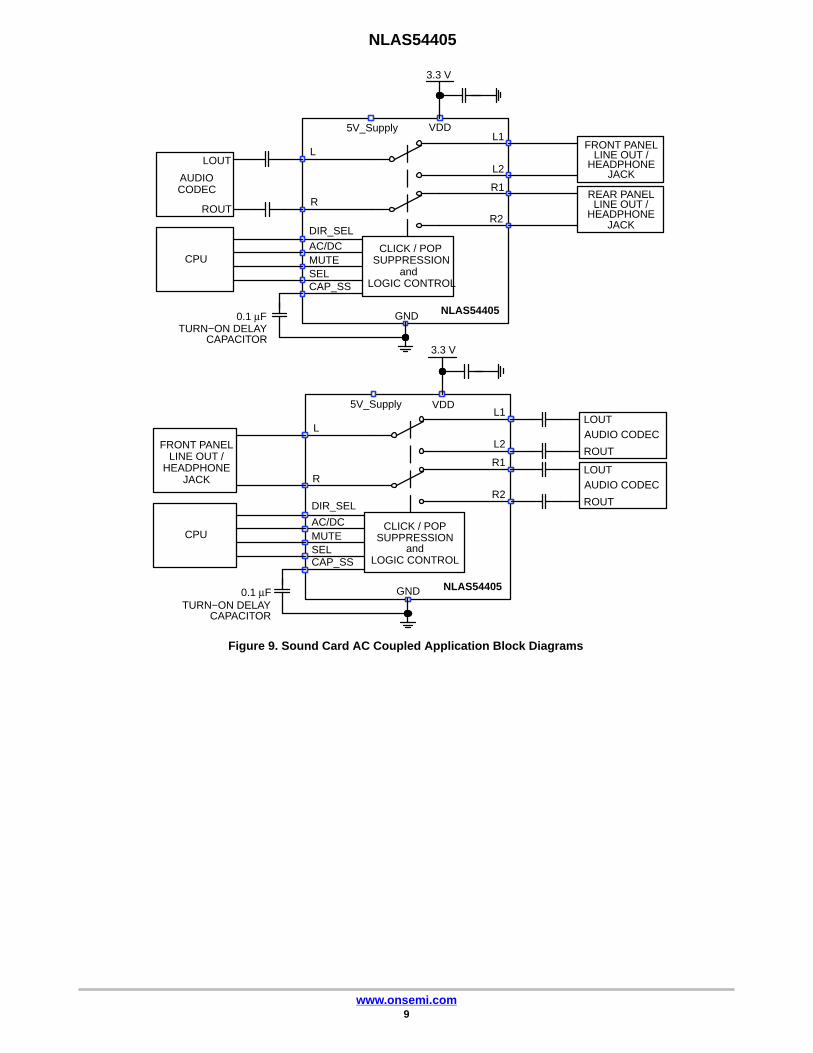
Figure 9. Sound Card AC Coupled Application Block Diagrams
CLICK / POPSUPPRESSION
andLOGIC CONTROL
5V_Supply VDD
L
R
CAP_SS
GND
L1
L2
R1
R2
0.1 μF
3.3 V
FRONT PANELLINE OUT /
HEADPHONEJACK
REAR PANELLINE OUT /
HEADPHONEJACK
AUDIOCODEC
CPU
ROUT
LOUT
NLAS54405
TURN−ON DELAYCAPACITOR
CLICK / POPSUPPRESSION
andLOGIC CONTROL
5V_Supply VDD
L
R
CAP_SS
GND
L1
L2
R1
R2
0.1 μF
3.3 V
AUDIO CODECFRONT PANEL
LINE OUT /HEADPHONE
JACK
CPU
ROUT
LOUT
AUDIO CODEC
ROUT
LOUT
NLAS54405
TURN−ON DELAYCAPACITOR
SELMUTEAC/DCDIR_SEL
SELMUTEAC/DC
DIR_SEL

NLAS54405
www.onsemi.com10
Detailed Description
The NLAS54405 is a single supply, bidirectional, dualsingle pole/double throw (SPDT) ultra−low distortion, highOFF−Isolation analog switch. It was designed to operatefrom either a 3.3 V or 5 V single supply. When operated witha 3.3 V or 5 V single supply, the switches can accommodate±2.828 VPEAK (2 VRMS) ground−referenced analog signals.The switch rON flatness across this range is extremely smallresulting in excellent THD+N performance (0.0002% with20 k� load and 0.0005% with 32 � load at 707 mVRMS).The T−Type configuration of the switch cells preventssignals from getting through to the output when a switch isin the OFF−state providing for superior mute performance(>107 dB) in audio applications.
The NLAS54405 has special circuitry to eliminate clickand pops in the speakers during power−up and power−downof the audio CODEC drivers, during removal and insertionof headphones, and while switching between sources andloads. The NLAS54405 was designed primarily forconsumer and professional audio switching applicationssuch as computer sound cards and home theater products.The “Sound Card AC Coupled Application BlockDiagrams” show two typical sound card applications. In theupper block diagram, the NLAS54405 is being used to routea single stereo source to either the front or back panel lineouts of the computer sound card. In the lower block diagram,the NLAS54405 is being used to multiplex two stereosources to a single line out of the computer sound card.
SPDT Switch Cell Architecture and PerformanceCharacteristics
The normally open (L2, R2) and normally closed (L1, R1)of the SPDT switches are T−Type switches that have atypical rON of 2.1 � and an OFF−isolation of > 107 dB. Thelow on−resistance (2.1 � and rON flatness (0.047 �) providevery low insertion loss and minimal distortion toapplications that require hi−fidelity signal reproduction.
The SPDT switch cells have internal charge pumps thatallow for signals to swing below ground. They werespecifically designed to pass audio signals that are groundreferenced and have a swing of ±2.828 VPEAK while drivingeither 10 k / 20 k� (receiver) or 32 � (headphone) loads.
Each switch cell incorporates special circuitry to delay theswitch transition from the OFF−state (high impedance) tothe ON−state (2.1 �). This delayed turn−on may help reduceclicks and pops in the speaker by matching turn−on time totransient switching events. The delayed turn−on time isdetermined by the capacitor value of the delayed turn−oncapacitor connected at the CAP_SS pin, the speaker load andthe DC level of the audio signal. With a 0.1 �F ceramic chipcapacitor, a 32 � load and 1.5 V DC level, the delayedturn−on is approximately 1700 �s. The delayed turn−on maybe disabled by floating the CAP_SS pin.
In addition to the delayed turn−on feature of the in lineswitches, the part has special click and pop (C/P) shunt
circuitry at each of the signal pins (L, R, L1, L2, R1, and R2).A pin’s C/P shunt circuitry is activated or deactivateddepending on the logic levels applied at the AC/DC andDIR_SEL control pins. This shunt circuitry serves twofunctions:
1. In an AC coupled application, they are activatedand directed to the source side of the switch tosuppress or eliminate click/pop noise in thespeaker load when powering up or down of theaudio CODEC drivers.
2. For superior muting, the C/P shunt circuitry isactivated and directed to the load side of theswitch which gives >107 dB of OFF−Isolationwhen driving a 10 k / 20 k� receiver load with anaudio signal in the range of 20 Hz to 22 kHz.
If the AC/DC pin is driven LOW, all C/P shunt circuitryat all the signal pins (L, R, L1, R1, L2, and R2) are deactivatedand not operable.
If the AC/DC pin is driven HIGH, then the logic at theDIR_SEL pin will determine whether the L and R (COM)C/P shunt circuitry is activated or the L1, L2, R1, and R2(NOx, NCx) C/P shunt circuitry is activated. When theDIR_SEL is driven LOW, the L1, R1, L2, R2 C/P shuntcircuitry will be activated while the L and R C/P shuntcircuitry will be deactivated. When the DIR_SEL is drivenHIGH, the L and R C/P shunt circuitry will be activatedwhile the L1, R1, L2, R2 C/P shunt circuitry will bedeactivated. Note: Shunt circuitry that is activated will beturned ON when a switch cell is turned OFF and will be OFFwhen a switch cell is turned ON.
Supply Voltage, Signal Amplitude, and GroundingThe power supply connected at VDD or the 5 V_Supply
pin provides power to the NLAS54405 part. TheNLAS54405 is a single supply device that was designed tobe operated with a 3.3 V ±10% DC supply connected at theVDD pin or a 5 V ±10% DC supply connected at the5 V_Supply pin.
It was specifically designed to accept ground referenced2 VRMS (±2.828 VPEAK) audio signals at its signal pinswhile driving either 10 k / 20 k� receiver loads or 32 �
headphone loads.When using the part in a 3.3 V application, the
5 V_Supply pin should be left floating. A 0.1 �F decouplingcapacitor should be connected from the VDD pin to groundto minimize power supply noise and transients. Thiscapacitor should be located as close to the pin as possible.
The part also has a 5 V supply pin (5 V_Supply) to allowit to be used in 5 V ±10% applications. Special circuitrywithin the device converts the 5 V, connected at the5 V_Supply pin, to 3.3 V to properly power the internalcircuitry of the device.
When using the part in a 5 V application, the VDD pinshould be left floating. A 0.1 �F decoupling capacitor should

NLAS54405
www.onsemi.com11
be connected from the 5 V_Supply pin to ground tominimize power supply noise. This capacitor should belocated as close to the pin as possible.
Grounding of the NLAS54405 should follow a starconfiguration (see Figure 10). All grounds of the IC shouldbe directly connected to the power supply ground returnwithout cascading to other grounds. This configurationisolates shunt currents of the Click and Pop transients fromthe IC ground and optimizes device performance.
Figure 10. Star Grounding Configuration
CLICK / POPSUPPRESSION
andLOGIC CONTROL
5V_Supply VDD
L
R
GND1
L1
L2
R1
R2
NLAS54405
0.1 μF
3.3 V
GND2
GND3CAP_SSSELMUTEAC/DCDIR_SEL
Mute OperationWhen the MUTE logic pin is driven HIGH, the part will go
into the mute state. In the mute state, all switches of the SPDTsare open while the T−Shunt switches are closed. In addition,any activated click and pop shunt circuitry at the signal pinsis turned on. See “Logic Control” below for more details.
Mute to OnWhen the MUTE pin is driven LOW, the NLAS54405 will
transition to the ON−state in the following sequence:1. All active shunt switches turn off quickly.2. The resistance of the switches selected by the SEL
pin will turn on from their high OFF−resistance totheir ON−resistance of 2.1 � after a time delay. Thedelayed turn−on time is determined by the capacitorvalue of the delayed turn−on capacitor connectedat the CAP_SS pin, the speaker load and the DClevel of the audio signal. See Figures 30 and 31.
Table 3. SWITCH TURN−ON DELAY FOR A 32 � LOADCapacitor Value VIS DC Level Turn−On Delay
No Capacitor 1.5 V 27.4 �s
0.05 �F 1.5 V 543 �s
0.1 �F 1.5 V 1680 �s
No Capacitor 60 mV 24.3 �s
0.05 �F 60 mV 38 �s
0.1 �F 60 mV 50 �s
Table 3 indicates how mute turn delay is affected by theCAP_SS capacitor value and the switch input DC voltagelevel.
On to MuteWhen the MUTE pin is driven HIGH, the switches will
turn off quickly (50 ns) and the active shunt switches willturn on quickly.
Off−Isolation in the Mute StateWhen in the mute state, the level of OFF−Isolation across
the audio band is dependent on the signal amplitude,external loading, and location of the activated C/P(click/pop) shunt circuitry. During muting, the logic of theNLAS54405 can be configured to activate the C/P shuntcircuitry on the load side of the switch or on the source sideof the switch, or deactivated on both sides of the switch.
With a 0.707 VRMS signal driving a 32 � headphone load,the location of the C/P shunt circuitry has little effect on theoff−isolation performance (>109 dB of off−isolation in allconfigurations), see Figure 12.
With a 2 VRMS signal driving a 20 k� amplifier load, thebest OFF−Isolation is achieved by placing the C/P shuntcircuitry on the load side of the switch (>120 dB across theaudio band).
Note: For AC coupled applications, when powering up ordown of the audio drivers, the C/P shunts should be activatedon the source side of the switch. See “Click and PopOperation”.
When using the switch for muting of the audio signal, theC/P shunt circuitry should be deactivated on the source sideof the switch and directed to the load side of the switch forbest possible OFF−Isolation.
Logic ControlThe NLAS54405 has four logic control pins; the AC/DC,
DIR_SEL, MUTE, and SEL. The MUTE and SEL controlpins determine the state of the switches. The AC/DC andDIR_SEL control pins determine the location of the C/P(click/pop) shunt circuitry and if it will be active or not. See“Truth Table”.
The NLAS54405 logic is 1.8 V CMOS compatible (Low� 0.5 V and High � 1.4 V) over a supply range of 3.0 V to3.6 V at the VDD pin or 4.5 V to 5.5 V at the 5 V_Supply pin.This allows control via 1.8 V or 3 V �−controller.
SEL, Mute Control PinsThe state of the SPDT switches of the NLAS54405 device
is determined by the voltage at the MUTE pin and the SELpin. The SEL control pin is only active when MUTE is logic“0”. The MUTE has an internal pull−up resistor to theinternal 3.3V supply rail and can be driven HIGH ortri−stated (floated) by the �−processor.
These pins are 1.8 V logic compatible. When poweringthe part by the VDD pin, the logic voltage can be as high asthe VDD voltage which is typically 3.3 V. When poweringthe part by the 5 V_Supply pin, the logic voltage can be ashigh as the 5 V_Supply voltage which is typically 5 V.

NLAS54405
www.onsemi.com12
Logic Levels:
MUTE = Logic “0” (Low) when � 0.5 V
MUTE = Logic “1” (High) when � 1.4 V or floating
SEL = Logic “0” (Low) when � 0.5 V
SEL = Logic “1” (High) when � 1.4 V
AC/DC and DIR_SEL Control PinsThe NLAS54405 contains C/P (click/pop) shunt circuitry
on its COM pins (L, R) and on its signal pins (L1, R1, L2, R2).The activation of this circuitry and whether it is located onthe COM or signal side of the switch is determined by thelogic levels applied at the AC/DC and DIR_SEL pins. TheDIR_SEL control pin is only active when AC/DC is logic“1”.
Note: Any activated C/P shunt circuitry is ON when in themute state (MUTE = Logic “1”) and OFF in the audio state(MUTE = Logic “0”).
When AC/DC is logic “0”, all of the C/P shunt circuitryon both sides of the switch is deactivated and not operable.
When AC/DC is logic “1”, then the DIR_SEL logic leveldetermines whether the shunt circuitry will be activated onthe COM side of the switch or on the signal side of theswitch. When DIR_SEL = Logic “1”, the C/P shunts on theCOM side (L,R) are activated and inoperable on the signalside (L1, R1, L2, R2) of the switch. When DIR_SEL = Logic“0”, the C/P shunts are activated on the signal side (L1, R1,L2, R2) and inoperable on the COM side (L, R).
Logic Levels:
AC/DC, DIR_SEL = Logic “0” (Low) when � 0.5 V
AC/DC, DIR_SEL = Logic “1” (High) when � 1.4 V orFloating.
The AC/DC and DIR_SEL have internal pull−up resistorsto the internal 3.3 V supply rail and can be driven HIGH ortri−stated (floated by the �−processor). They should bedriven to ground for a logic “0” (Low).
Note: For 5 V applications, the AC/DC and DIR_SEL pinsshould never be driven to the external 5 V rail. They need tobe driven with 1.8 V logic or 3 V logic circuit.
AC Coupled or DC Coupled OperationThe Audio CODEC drivers can be directly coupled to the
NLAS54405 when the audio signals from the drivers areground referenced or do not have a significant DC offsetvoltage, <50 mV. Otherwise, the signal should be ACcoupled to the NLAS54405 part.
Click and Pop OperationThe NLAS54405 has special circuitry to eliminate click
and pops in the speakers during power−up and power−downof the Audio CODEC Drivers and during removal andinsertion of headphones.
A different click and pop scheme is required depending onwhether the audio CODEC drivers are AC coupled or DCcoupled to the inputs of the NLAS54405 part.
AC Coupled Click and Pop OperationSingle supply audio drivers have their signal biased at a
DC offset voltage, usually at 1/2 the DC supply voltage ofthe driver. As this DC bias voltage comes up or goes downduring power up or down of the driver, a transient can becoupled into the speaker load through the DC blockingcapacitor (see the “Sound Card AC Coupled ApplicationBlock Diagrams”).
When a driver is off and suddenly turned on, the rapidlychanging DC bias voltage at the output of the driver willcause an equal voltage at the input side of the switch due tothe fact that the voltage across the blocking capacitor cannotchange instantly. If the switch is in audio mode or there is nolow impedance path to discharge the capacitor voltage at theinput of the switch, before turning on the switch, a transientdischarge will occur in the speaker, generating a click andpop noise.
Proper elimination of a click/pop transient at the speakerload while powering up or down of the audio driver requiresthat the NLAS54405 have its C/P shunts activated on thesource side of the switch and then placed in mute mode. Thisallows the transient generated by the audio drivers to bedischarged through the click and pop shunt circuitry.
Once the driver DC bias has reached VDD/2 and thetransient on the switch side of the DC blocking capacitor hasbeen discharged to ground through the C/P shunt circuitry,the switches can be turned on and connected through to thespeaker loads without generating an undesirable click/pop inthe speakers.
With a typical DC blocking capacitor of 220 �F and theC/P shunt circuitry designed to have a resistance of 40 �,allowing a 100 ms wait time to discharge the transient beforeplacing the switch in the audio mode, will prevent thetransient from getting through to the speaker load. SeeFigures 28 and 29.
Click and Pop Elimination when Connected to HighImpedance Source and Load
By design, in order to flatten the RON resistance of theswitch across the signal range (±3 V) a current gets added tothe signal path. When the NLAS54405 part is connected toa high impedance source (i.e. AC coupled to the input of theswitch) and a high impedance load, (such as the impedanceof a 20 k� to 100 k� preamplifier stage) a DC offset voltagewill be present on the signal line in the range of 35 mV to135 mV.
When the switch is turned off, this offset voltage getspulled to ground. During switching, this change in the offsetvoltage can cause a click and pop noise to be heard in thedownstream speaker.
Placing a 1 k� resistor from the output of the switch toground will lower the offset voltage to around 1.5 mV,thereby effectively eliminating the click and pop noise. The1 k� resistor is small enough to reduce the voltage offsetsignificantly while not increasing power dissipation

NLAS54405
www.onsemi.com13
dramatically. Power consumption will need to be consideredwhen using a smaller impedance under this scenario.
When connected to a low impedance load such asheadphones (32 �), the current added to the signal line resultsin a minimal DC offset voltage on the signal line and doesnot cause click and pop noise when the switch is turned off.
DC Coupled Click and Pop OperationThe NLAS54405 can pass ground−referenced audio
signals which allows it to be directly connected to audiodrivers that output ground−referenced audio signals,eliminating the need for a DC blocking capacitor.
Audio drivers that swing around ground, however, dogenerate some DC offset, from a few millivolts to tens ofmillivolts. When switching between audio channels ormuting the audio signal, these small DC offset levels of thedrivers can generate a transient that can cause unwantedclicks and pops in the speaker loads.
In a DC coupled application, the C/P shunt resistorsplaced at the source side of the switch have no effect ineliminating the transients at the speaker loads whentransitioning in and out of the mute state or switchingbetween channels. In fact, having these C/P shunts active onthe source side unnecessarily increases the powerconsumption. So, for DC coupled connection, the C/P shuntcircuitry should not be applied at the source (driver) side ofthe switch.
For DC coupled applications, the NLAS54405 has aspecial turn−on delay feature that delays the connectionfrom the audio driver output to the speaker load whenturning on a switch channel. The delayed turn−on time isdetermined by the capacitor value of the delayed turn−oncapacitor connected at the CAP_SS pin, the speaker load andthe DC level of the audio signal.
The turn−on delay may help reduce clicks and pops in thespeaker by matching turn−on time to transient switchingevents. A delayed turn−on capacitor value of 0.1 �F, coupledwith a 32 � load and a 1.5 V DC level, provides a turn−ondelayed of approximately 1700 �s. See Figures 30 and 31.See “MUTE to ON” section for more detail of how turn−ondelay works.
Supply Sequencing and Overvoltage ProtectionWith any CMOS device, proper power supply sequencing
is required to protect the device from excessive inputcurrents which might permanently damage the IC. All I/Opins contain ESD protection diodes or diode stacks from thepin to VDD and to GND (see Figure 11). To prevent forwardbiasing these diodes, VDD must be applied before any inputsignals, and the signal voltages must remain between VDDand −3 V and the logic voltage must remain between VDDand ground.
If these conditions cannot be guaranteed, then precautionsmust be implemented to prohibit the current and voltage at
the logic pin and signal pins from exceeding the maximumratings of the switch. The following two methods can beused to provided additional protection to limit the current inthe event that the voltage at a signal pin goes below groundby more than −3 V or above the VDD rail and the logic pingoes below ground or above the VDD rail.
Logic inputs can be protected by adding a 1 k� resistor inseries with the logic input (see Figure 11). The resistor limitsthe input current below the threshold that producespermanent damage, and the sub−microamp input currentproduces an insignificant voltage drop during normaloperation.
This method is not acceptable for the signal path inputs.Adding a series resistor to the switch input defeats thepurpose of using a low rON switch. Connecting Schottkydiodes to the signal pins, as shown in Figure 11 will shunt thefault current to the supply or to ground thereby protecting theswitch. These Schottky diodes must be sized to handle theexpected fault current and to clamp when the voltage reachesthe overvoltage limit.
Figure 11. Overvoltage Protection
High−Frequency PerformanceIn 50 � systems, the NLAS54405 has a −3 dB bandwidth
of 450 MHz (see Figure 32). The frequency response is veryconsistent over varying analog signal levels.
An OFF−switch acts like a capacitor and passes higherfrequencies with less attenuation, resulting in signal feed−through from a switch’s input to its output. OFF−Isolation isthe resistance to this feed−through, while crosstalk indicatesthe amount of feed−through from one switch to another.Figure 33 details the high OFF−Isolation and crosstalkrejection provided by this part. At 1 MHz, Off−Isolation isabout 68 dB in 50 � systems, decreasing approximately20 dB per decade as frequency increases. Higher loadimpedances decrease OFF−Isolation and crosstalk rejectiondue to the voltage divider action of the switch off impedanceand the load impedance.

NLAS54405
www.onsemi.com14
TYPICAL CHARACTERISTICS
Figure 12. On−Resistance vs. Switch Voltage Figure 13. Off−Isolation, 2 VRMS Signal, 20 k�Load
Figure 14. Off−Isolation, 0.707 VRMS Signal,32 � Load
Figure 15. Channel−to−Channel Crosstalk
Figure 16. Channel−to−Channel Crosstalk Figure 17. Insertion Loss vs. Frequency

NLAS54405
www.onsemi.com15
TYPICAL CHARACTERISTICS
Figure 18. Gain vs. Frequency Figure 19. Stereo Imbalance vs. Frequency
Figure 20. THD+N vs. Signal Levels vs.Frequency
Figure 21. THD+N vs. Signal Levels vs.Frequency
Figure 22. THD+N vs. Signal Levels vs.Frequency
Figure 23. THD+N vs. Signal Levels vs.Frequency

NLAS54405
www.onsemi.com16
TYPICAL CHARACTERISTICS
Figure 24. THD+N vs. Signal Levels vs.Frequency
Figure 25. THD+N vs. Signal Levels vs.Frequency
Figure 26. PSRR vs. Frequency Figure 27. PSRR vs. Frequency
Figure 28. 20 k� AC Coupled Click / PopReduction
Figure 29. 32 � AC Coupled Click / PopReduction

NLAS54405
www.onsemi.com17
TYPICAL CHARACTERISTICS
Figure 30. Turn−on Delay (0.1 �F) Click/PopReduction
Figure 31. Turn−on Delay (0.05 �F) Click/PopReduction
Figure 32. Frequency Response Figure 33. Crosstalk and Off−Isolation

WQFN16, 1.8x2.6, 0.4PCASE 488AP−01
ISSUE BDATE 25 JUN 2008
ÉÉÉÉÉÉÉÉÉ
SCALE 5:1
A
b
A3A1
0.08 CSEATINGPLANE
NOTE 3
NOTES:1. DIMENSIONING AND TOLERANCING PER ASME
Y14.5M, 1994.2. CONTROLLING DIMENSION: MILLIMETERS3. DIMENSION b APPLIES TO PLATED TERMINAL
AND IS MEASURED BETWEEN 0.25 AND 0.30 MMFROM TERMINAL.
4. COPLANARITY APPLIES TO THE EXPOSED PADAS WELL AS THE TERMINALS.
5. EXPOSED PADS CONNECTED TO DIE FLAG.USED AS TEST CONTACTS.
DIM MIN MAXMILLIMETERS
A
1.80 BSC
A1
0.40 BSC
A3
0.70 0.80
bD
0.30 0.50
EeLL1
0.20 REF0.00 0.050
PIN 1 REFERENCE
1
D A
E
B
0.15 C2X
0.15 C2X
0.10 C
C
L2
1
4
5
0.05 C
0.10 C A B16 X
e
L15 X
0.00 0.15
2.60 BSC
0.15 0.25
MOUNTING FOOTPRINT8
12
9
16
� mminches
�SCALE 20:1
1
0.4000.0157
0.2250.0089
0.4630.0182
0.5620.0221
2.9000.1142
1.2000.0472
2.1000.0827
L1
DETAIL A
L
ALTERNATE TERMINALCONSTRUCTIONS
ÉÉÇÇA1
A3
L
ÉÉÉÉÉÉ
DETAIL B
MOLD CMPDEXPOSED Cu
ALTERNATECONSTRUCTIONS
DETAIL B
DETAIL A
L2 0.40 0.60
MECHANICAL CASE OUTLINE
PACKAGE DIMENSIONS
ON Semiconductor and are trademarks of Semiconductor Components Industries, LLC dba ON Semiconductor or its subsidiaries in the United States and/or other countries.ON Semiconductor reserves the right to make changes without further notice to any products herein. ON Semiconductor makes no warranty, representation or guarantee regardingthe suitability of its products for any particular purpose, nor does ON Semiconductor assume any liability arising out of the application or use of any product or circuit, and specificallydisclaims any and all liability, including without limitation special, consequential or incidental damages. ON Semiconductor does not convey any license under its patent rights nor therights of others.
98AON20790DDOCUMENT NUMBER:
DESCRIPTION:
Electronic versions are uncontrolled except when accessed directly from the Document Repository.Printed versions are uncontrolled except when stamped “CONTROLLED COPY” in red.
PAGE 1 OF 1WQFN16, 1.8 X 2.6, 0.4P
© Semiconductor Components Industries, LLC, 2019 www.onsemi.com

onsemi, , and other names, marks, and brands are registered and/or common law trademarks of Semiconductor Components Industries, LLC dba “onsemi” or its affiliatesand/or subsidiaries in the United States and/or other countries. onsemi owns the rights to a number of patents, trademarks, copyrights, trade secrets, and other intellectual property.A listing of onsemi’s product/patent coverage may be accessed at www.onsemi.com/site/pdf/Patent−Marking.pdf. onsemi reserves the right to make changes at any time to anyproducts or information herein, without notice. The information herein is provided “as−is” and onsemi makes no warranty, representation or guarantee regarding the accuracy of theinformation, product features, availability, functionality, or suitability of its products for any particular purpose, nor does onsemi assume any liability arising out of the application or useof any product or circuit, and specifically disclaims any and all liability, including without limitation special, consequential or incidental damages. Buyer is responsible for its productsand applications using onsemi products, including compliance with all laws, regulations and safety requirements or standards, regardless of any support or applications informationprovided by onsemi. “Typical” parameters which may be provided in onsemi data sheets and/or specifications can and do vary in different applications and actual performance mayvary over time. All operating parameters, including “Typicals” must be validated for each customer application by customer’s technical experts. onsemi does not convey any licenseunder any of its intellectual property rights nor the rights of others. onsemi products are not designed, intended, or authorized for use as a critical component in life support systemsor any FDA Class 3 medical devices or medical devices with a same or similar classification in a foreign jurisdiction or any devices intended for implantation in the human body. ShouldBuyer purchase or use onsemi products for any such unintended or unauthorized application, Buyer shall indemnify and hold onsemi and its officers, employees, subsidiaries, affiliates,and distributors harmless against all claims, costs, damages, and expenses, and reasonable attorney fees arising out of, directly or indirectly, any claim of personal injury or deathassociated with such unintended or unauthorized use, even if such claim alleges that onsemi was negligent regarding the design or manufacture of the part. onsemi is an EqualOpportunity/Affirmative Action Employer. This literature is subject to all applicable copyright laws and is not for resale in any manner.
PUBLICATION ORDERING INFORMATIONTECHNICAL SUPPORTNorth American Technical Support:Voice Mail: 1 800−282−9855 Toll Free USA/CanadaPhone: 011 421 33 790 2910
LITERATURE FULFILLMENT:Email Requests to: [email protected]
onsemi Website: www.onsemi.com
Europe, Middle East and Africa Technical Support:Phone: 00421 33 790 2910For additional information, please contact your local Sales Representative
◊