Embed Size (px)
Citation preview
Nixie Clock Development Board v1.3
User’s guide
Revision B-1
2
Table of contents 1. Introduction
1.1. Technical data ........................................................................... 4 1.2. Features ..................................................................................... 6 1.3. Block diagram ........................................................................... 7
2. Connectors 2.1. Tubes connectors....................................................................... 8 2.2. Programming connector ............................................................ 10 2.3. RS232 connector ....................................................................... 10 2.4. PS/2 connector........................................................................... 11 2.5. Power connector ........................................................................ 11 2.6. General purpose output and external switches .......................... 11
3. Functions implemented on the development board 3.1. High voltage drivers .................................................................. 12 3.2. In system programmer............................................................... 13 3.3. RS232 port................................................................................. 14 3.4. Real time clock.......................................................................... 15 3.5. Temperature sensor ................................................................... 16 3.6. Photo sensor and buzzer............................................................ 16 3.7. Power supply ............................................................................. 17 3.8. Buttons ...................................................................................... 18 3.9. Tube’s board.............................................................................. 18
4. Typical performance characteristics................................................. 19 5. Schematic diagram ........................................................................... 21
3
1. Introduction The “Nixie Clock Development Board v1.3” is first nixie clock experimenter's platform. This flexible, professionally designed development board is an ideal platform for any nixie clock project. While simple clock kit boards allow you to create your own projects with a minimum of hassle, the “Nixie Clock Development Board v1.3” goes one step further. It provides a test bed containing most of the circuitry commonly used by the Nixie clocks. Board has standard connectors for the tubes and adjustable power supply so any nixie tubes may be used. Many different projects such as: precise time base clock, GPS clock, heating system controller or coffee machine timer may be created using the “Nixie Clock Development Board v1.3”. Some examples written in C are included with the board as well as fully featured RTOS based firmware. The “Nixie Clock Development Board v1.3” is able to run programs written in assembler, C and PicBasic or PicBasic Pro. It also includes in-system programmer, so the resident PICmicroTM MCU may be reprogrammed on the fly. The Nixie Clock Development Board’s circuits and software (firmware) may not be reverse engineered, copied or used commercially without express written permission. PRECAUTION Relatively high voltage is generated on this board. Do not touch power supply, high voltage drivers and tube connections when clock is working. Otherwise is risk of electric shock.
4
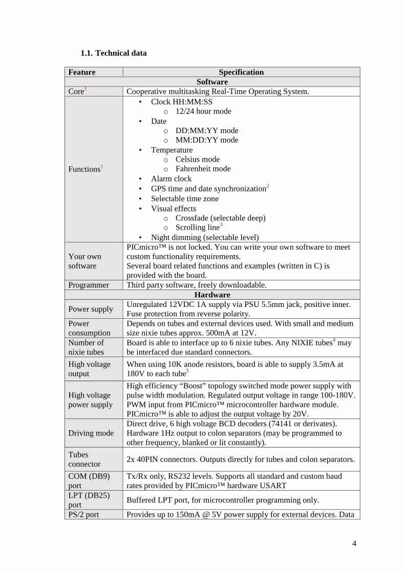
1.1. Technical data Feature Specification
Software Core1 Cooperative multitasking Real-Time Operating System.
Functions1
• Clock HH:MM:SS o 12/24 hour mode
• Date o DD:MM:YY mode o MM:DD:YY mode
• Temperature o Celsius mode o Fahrenheit mode
• Alarm clock • GPS time and date synchronization2 • Selectable time zone • Visual effects
o Crossfade (selectable deep) o Scrolling line3
• Night dimming (selectable level)
Your own software
PICmicro™ is not locked. You can write your own software to meet custom functionality requirements. Several board related functions and examples (written in C) is provided with the board.
Programmer Third party software, freely downloadable. Hardware
Power supply Unregulated 12VDC 1A supply via PSU 5.5mm jack, positive inner. Fuse protection from reverse polarity.
Power consumption
Depends on tubes and external devices used. With small and medium size nixie tubes approx. 500mA at 12V.
Number of nixie tubes
Board is able to interface up to 6 nixie tubes. Any NIXIE tubes4 may be interfaced due standard connectors.
High voltage output
When using 10K anode resistors, board is able to supply 3.5mA at 180V to each tube5
High voltage power supply
High efficiency “Boost” topology switched mode power supply with pulse width modulation. Regulated output voltage in range 100-180V. PWM input from PICmicro™ microcontroller hardware module. PICmicro™ is able to adjust the output voltage by 20V.
Driving mode Direct drive, 6 high voltage BCD decoders (74141 or derivates). Hardware 1Hz output to colon separators (may be programmed to other frequency, blanked or lit constantly).
Tubes connector 2x 40PIN connectors. Outputs directly for tubes and colon separators.
COM (DB9) port
Tx/Rx only, RS232 levels. Supports all standard and custom baud rates provided by PICmicro™ hardware USART
LPT (DB25) port Buffered LPT port, for microcontroller programming only.
PS/2 port Provides up to 150mA @ 5V power supply for external devices. Data
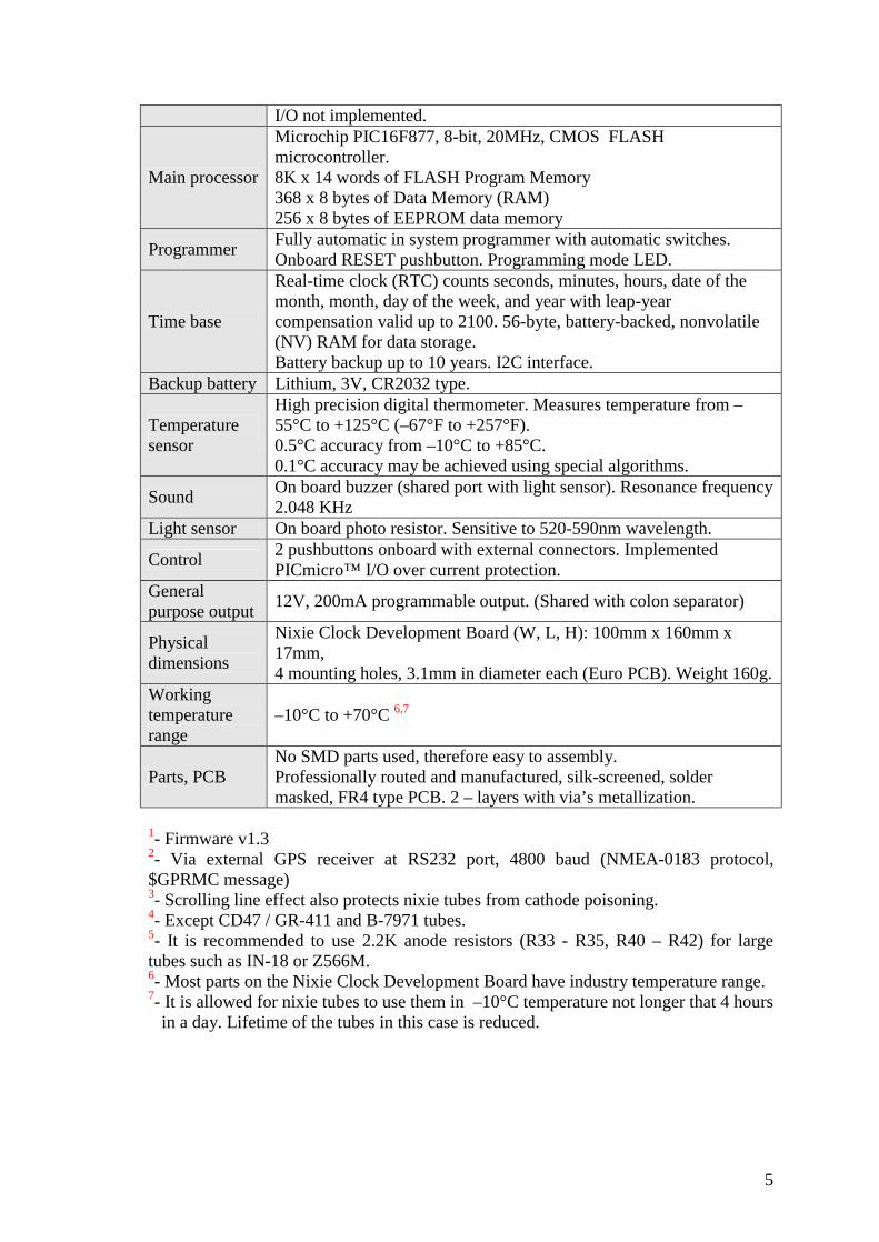
5
I/O not implemented.
Main processor
Microchip PIC16F877, 8-bit, 20MHz, CMOS FLASH microcontroller. 8K x 14 words of FLASH Program Memory 368 x 8 bytes of Data Memory (RAM) 256 x 8 bytes of EEPROM data memory
Programmer Fully automatic in system programmer with automatic switches. Onboard RESET pushbutton. Programming mode LED.
Time base
Real-time clock (RTC) counts seconds, minutes, hours, date of the month, month, day of the week, and year with leap-year compensation valid up to 2100. 56-byte, battery-backed, nonvolatile (NV) RAM for data storage. Battery backup up to 10 years. I2C interface.
Backup battery Lithium, 3V, CR2032 type.
Temperature sensor
High precision digital thermometer. Measures temperature from –55°C to +125°C (–67°F to +257°F). 0.5°C accuracy from –10°C to +85°C. 0.1°C accuracy may be achieved using special algorithms.
Sound On board buzzer (shared port with light sensor). Resonance frequency 2.048 KHz
Light sensor On board photo resistor. Sensitive to 520-590nm wavelength.
Control 2 pushbuttons onboard with external connectors. Implemented PICmicro™ I/O over current protection.
General purpose output 12V, 200mA programmable output. (Shared with colon separator)
Physical dimensions
Nixie Clock Development Board (W, L, H): 100mm x 160mm x 17mm, 4 mounting holes, 3.1mm in diameter each (Euro PCB). Weight 160g.
Working temperature range
–10°C to +70°C 6,7
Parts, PCB No SMD parts used, therefore easy to assembly. Professionally routed and manufactured, silk-screened, solder masked, FR4 type PCB. 2 – layers with via’s metallization.
1- Firmware v1.3 2- Via external GPS receiver at RS232 port, 4800 baud (NMEA-0183 protocol, $GPRMC message) 3- Scrolling line effect also protects nixie tubes from cathode poisoning. 4- Except CD47 / GR-411 and B-7971 tubes. 5- It is recommended to use 2.2K anode resistors (R33 - R35, R40 – R42) for large tubes such as IN-18 or Z566M. 6- Most parts on the Nixie Clock Development Board have industry temperature range. 7- It is allowed for nixie tubes to use them in –10°C temperature not longer that 4 hours
in a day. Lifetime of the tubes in this case is reduced.
6
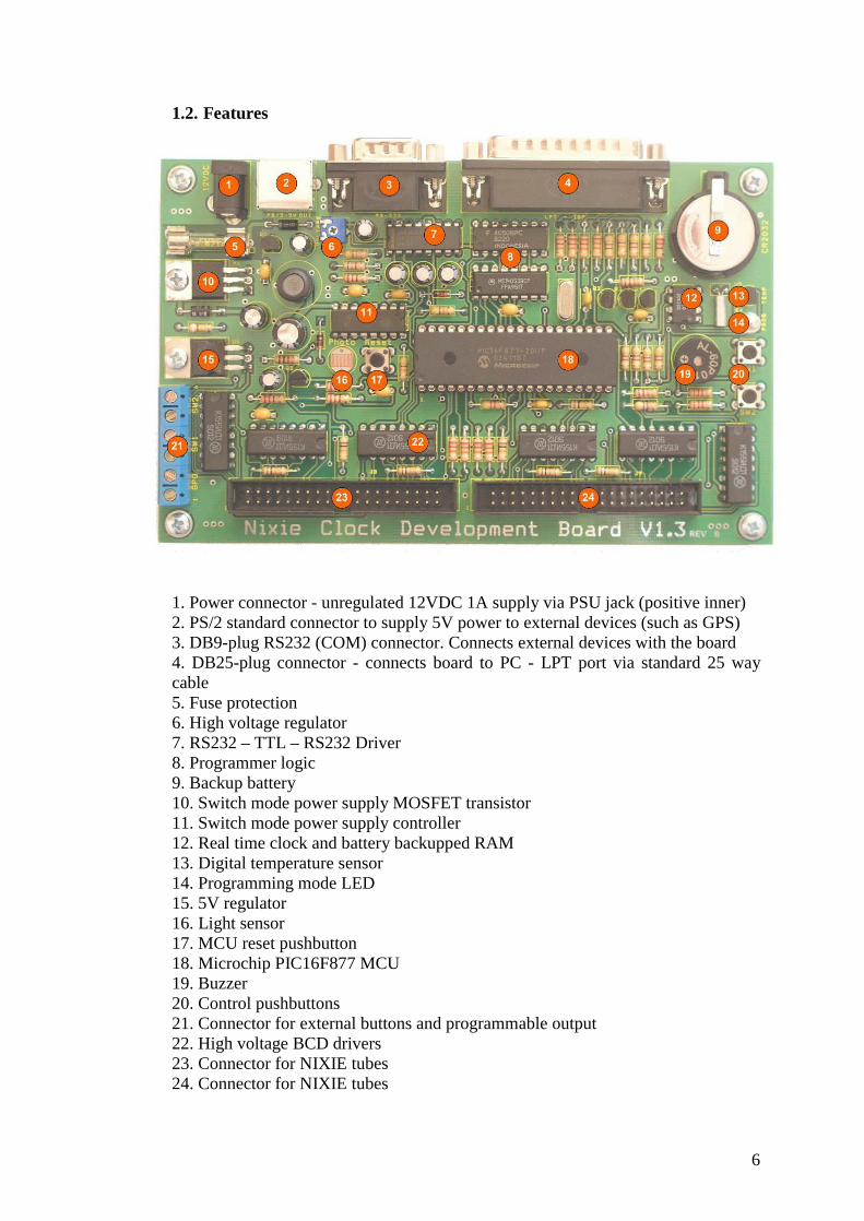
1.2. Features
1. Power connector - unregulated 12VDC 1A supply via PSU jack (positive inner) 2. PS/2 standard connector to supply 5V power to external devices (such as GPS) 3. DB9-plug RS232 (COM) connector. Connects external devices with the board 4. DB25-plug connector - connects board to PC - LPT port via standard 25 way cable 5. Fuse protection 6. High voltage regulator 7. RS232 – TTL – RS232 Driver 8. Programmer logic 9. Backup battery 10. Switch mode power supply MOSFET transistor 11. Switch mode power supply controller 12. Real time clock and battery backupped RAM 13. Digital temperature sensor 14. Programming mode LED 15. 5V regulator 16. Light sensor 17. MCU reset pushbutton 18. Microchip PIC16F877 MCU 19. Buzzer 20. Control pushbuttons 21. Connector for external buttons and programmable output 22. High voltage BCD drivers 23. Connector for NIXIE tubes 24. Connector for NIXIE tubes
7
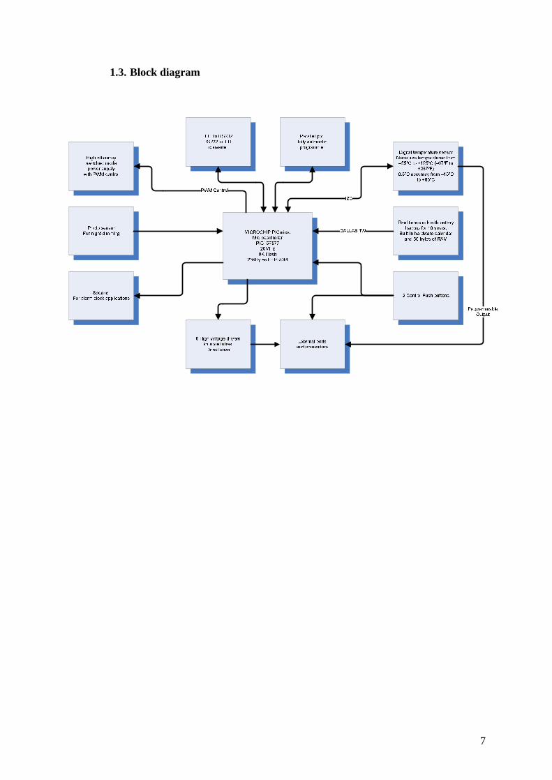
1.3. Block diagram
8
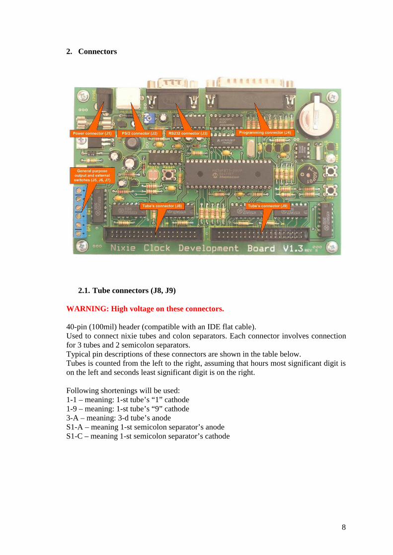
2. Connectors
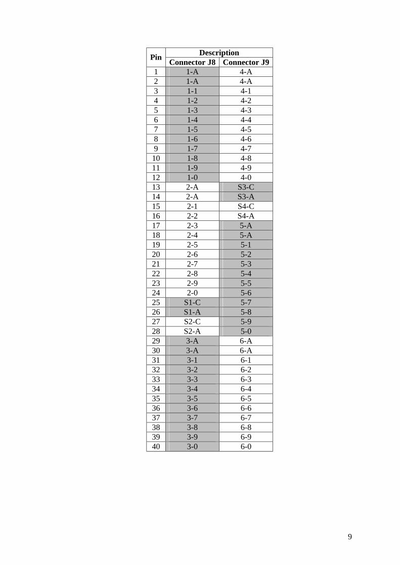
2.1. Tube connectors (J8, J9) WARNING: High voltage on these connectors. 40-pin (100mil) header (compatible with an IDE flat cable). Used to connect nixie tubes and colon separators. Each connector involves connection for 3 tubes and 2 semicolon separators. Typical pin descriptions of these connectors are shown in the table below. Tubes is counted from the left to the right, assuming that hours most significant digit is on the left and seconds least significant digit is on the right. Following shortenings will be used: 1-1 – meaning: 1-st tube’s “1” cathode 1-9 – meaning: 1-st tube’s “9” cathode 3-A – meaning: 3-d tube’s anode S1-A – meaning 1-st semicolon separator’s anode S1-C – meaning 1-st semicolon separator’s cathode
9
Description Pin Connector J8 Connector J9 1 1-A 4-A 2 1-A 4-A 3 1-1 4-1 4 1-2 4-2 5 1-3 4-3 6 1-4 4-4 7 1-5 4-5 8 1-6 4-6 9 1-7 4-7 10 1-8 4-8 11 1-9 4-9 12 1-0 4-0 13 2-A S3-C 14 2-A S3-A 15 2-1 S4-C 16 2-2 S4-A 17 2-3 5-A 18 2-4 5-A 19 2-5 5-1 20 2-6 5-2 21 2-7 5-3 22 2-8 5-4 23 2-9 5-5 24 2-0 5-6 25 S1-C 5-7 26 S1-A 5-8 27 S2-C 5-9 28 S2-A 5-0 29 3-A 6-A 30 3-A 6-A 31 3-1 6-1 32 3-2 6-2 33 3-3 6-3 34 3-4 6-4 35 3-5 6-5 36 3-6 6-6 37 3-7 6-7 38 3-8 6-8 39 3-9 6-9 40 3-0 6-0
10
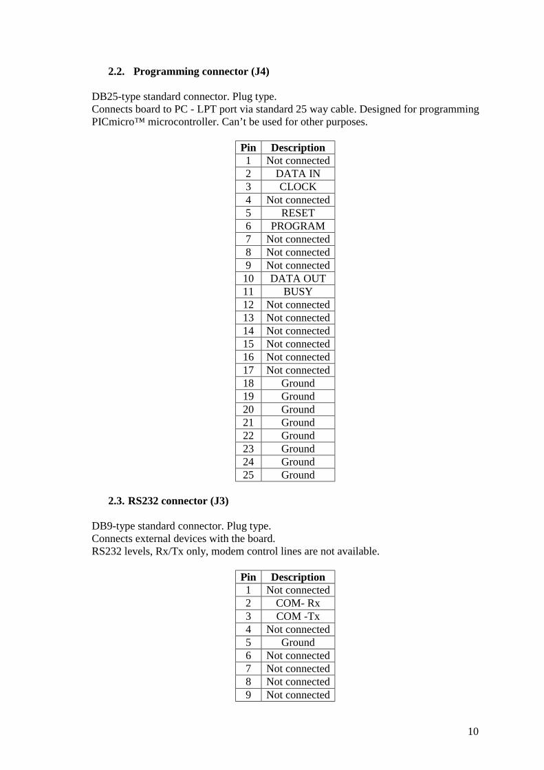
2.2. Programming connector (J4) DB25-type standard connector. Plug type. Connects board to PC - LPT port via standard 25 way cable. Designed for programming PICmicro™ microcontroller. Can’t be used for other purposes.
Pin Description 1 Not connected 2 DATA IN 3 CLOCK 4 Not connected 5 RESET 6 PROGRAM 7 Not connected 8 Not connected 9 Not connected 10 DATA OUT 11 BUSY 12 Not connected 13 Not connected 14 Not connected 15 Not connected 16 Not connected 17 Not connected 18 Ground 19 Ground 20 Ground 21 Ground 22 Ground 23 Ground 24 Ground 25 Ground
2.3. RS232 connector (J3)
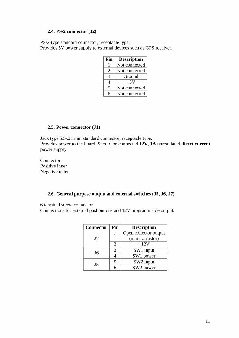
DB9-type standard connector. Plug type. Connects external devices with the board. RS232 levels, Rx/Tx only, modem control lines are not available.
Pin Description 1 Not connected 2 COM- Rx 3 COM -Tx 4 Not connected 5 Ground 6 Not connected 7 Not connected 8 Not connected 9 Not connected
11
2.4. PS/2 connector (J2) PS/2-type standard connector, receptacle type. Provides 5V power supply to external devices such as GPS receiver.
Pin Description 1 Not connected 2 Not connected 3 Ground 4 +5V 5 Not connected 6 Not connected
2.5. Power connector (J1) Jack type 5.5x2.1mm standard connector, receptacle type. Provides power to the board. Should be connected 12V, 1A unregulated direct current power supply. Connector: Positive inner Negative outer
2.6. General purpose output and external switches (J5, J6, J7) 6 terminal screw connector. Connections for external pushbuttons and 12V programmable output.
Connector Pin Description
1 Open collector output (npn transistor) J7
2 +12V 3 SW1 input J6 4 SW1 power 5 SW2 input J5 6 SW2 power
12
3. Functions implemented on the development board
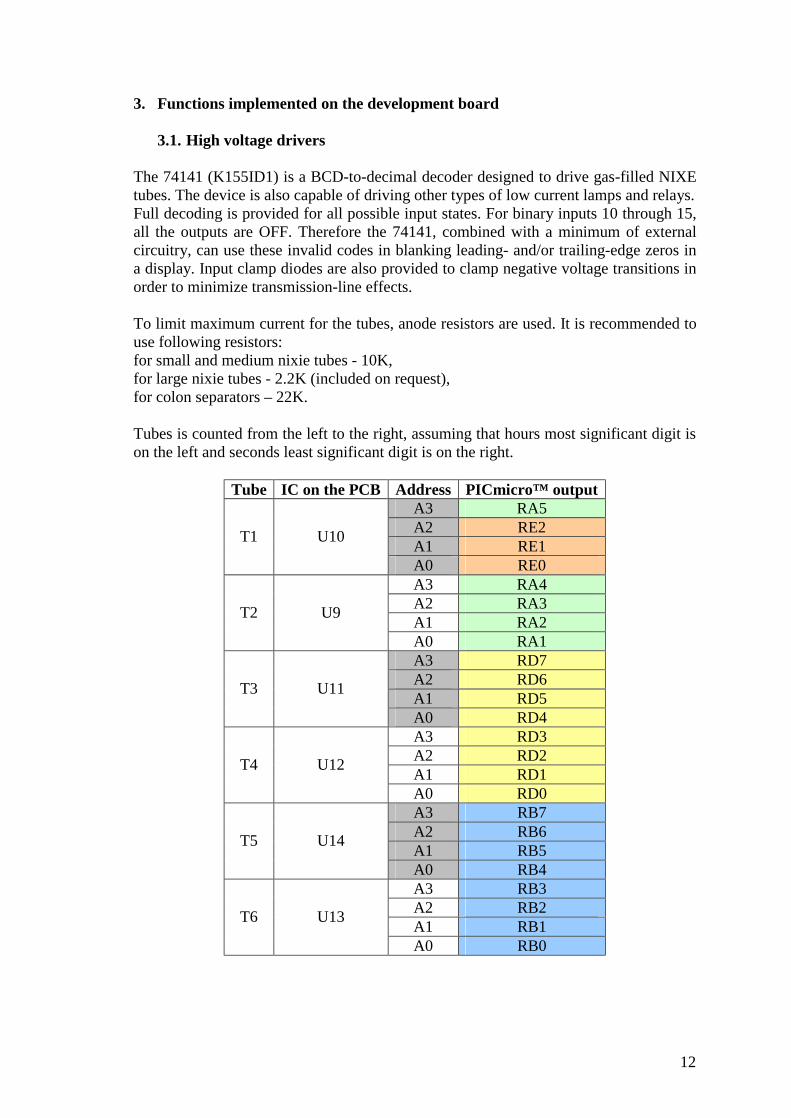
3.1. High voltage drivers The 74141 (K155ID1) is a BCD-to-decimal decoder designed to drive gas-filled NIXE tubes. The device is also capable of driving other types of low current lamps and relays. Full decoding is provided for all possible input states. For binary inputs 10 through 15, all the outputs are OFF. Therefore the 74141, combined with a minimum of external circuitry, can use these invalid codes in blanking leading- and/or trailing-edge zeros in a display. Input clamp diodes are also provided to clamp negative voltage transitions in order to minimize transmission-line effects. To limit maximum current for the tubes, anode resistors are used. It is recommended to use following resistors: for small and medium nixie tubes - 10K, for large nixie tubes - 2.2K (included on request), for colon separators – 22K. Tubes is counted from the left to the right, assuming that hours most significant digit is on the left and seconds least significant digit is on the right.
Tube IC on the PCB Address PICmicro™ output A3 RA5 A2 RE2 A1 RE1 T1 U10
A0 RE0 A3 RA4 A2 RA3 A1 RA2 T2 U9
A0 RA1 A3 RD7 A2 RD6 A1 RD5 T3 U11
A0 RD4 A3 RD3 A2 RD2 A1 RD1 T4 U12
A0 RD0 A3 RB7 A2 RB6 A1 RB5 T5 U14
A0 RB4 A3 RB3 A2 RB2 A1 RB1 T6 U13
A0 RB0

13
3.2. In system programmer
0
R5
22kR14
22k
0
0
0
VCC5
0
0
RB6
R6470
J4
CONNECTOR DB25
13251224112310229218207196185174163152141
RESET
R20
4.7k
SW3
0
D212V Zener
R8
4.7k
Q2
2SA1266
R747k
0
PGM_SIGNAL
PGM_OUT
Q42N2222
R4
22k
0
R25
220
R3
22k
VCC5
RB7
0 0
R10220
U3
4053
12345678 9
10111213141516
2Y12Y03Y13Z3Y0~EVeeGnd S3
S2S1
1Y01Y1
1Z2Z
Vcc
VCC5
0
R94.7k
0
0
U2
4050
12345678 9
10111213141516
Vcc1Y1A2Y2A3Y3AGnd 4A
4Y5A5Y
N C6A6YNC
R2
22k
VCC12
D4
LED
Q32N2222
SEC_HI_NIB_A3
SEC_HI_NIB_A2
MCLR
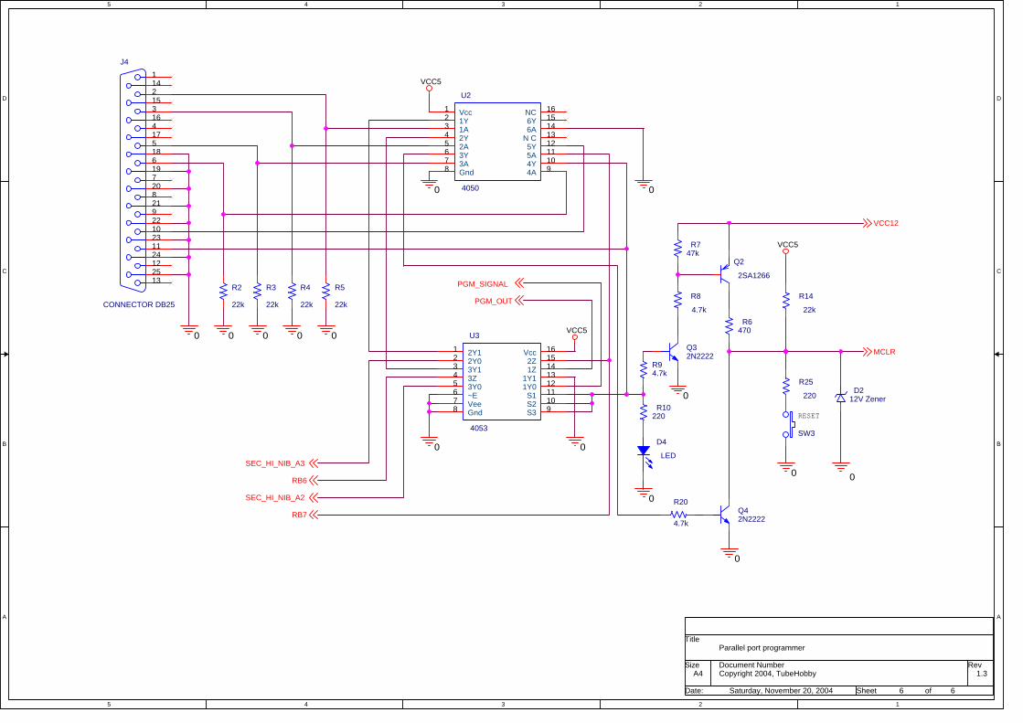
Signals from the PC are buffered, to ensure consistent voltage levels, by U2 - a 4050. The pins RB6 and RB7 are used on the PICmicro™ device for both programming and reading data and the PC needs direct control of these devices. This is facilitated by the use of two analogue switches U3:2 and U3:3 which are controlled by the program pin (pin 6) on the parallel port via U2:4. When the program pin is high, data in and clock in are directed to the PICmicro™. When the program pin is low then RB6 and RB7 on the PICmicro™ are routed to the rest of the port B bus. The program pin also ensures that 12V is routed to the PICmicro™ via the combination of Q2 and Q3 using zener diode to provide a regulated programming voltage. Automatic reset after programming is provides by the reset line from the parallel port (pin 5) and Q4.
14
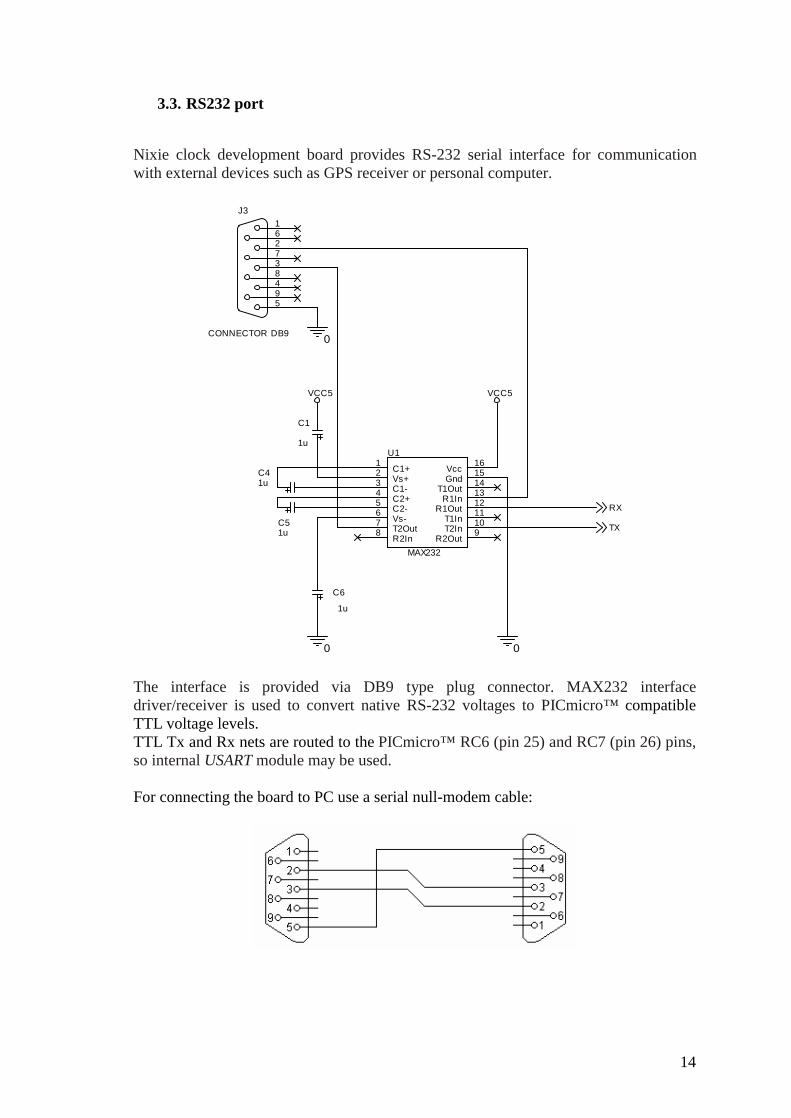
3.3. RS232 port Nixie clock development board provides RS-232 serial interface for communication with external devices such as GPS receiver or personal computer.
VCC5
0
RX
VCC5
0
C51u
C41u
U1
MAX232
12345678 9
10111213141516C1+
Vs+C1-C2+C2-Vs-T2OutR2In R2Out
T2InT1In
R1OutR1In
T1OutGndVcc
J3
CONNECTOR DB9
594837261
0
TX
C1
1u
C6
1u
The interface is provided via DB9 type plug connector. MAX232 interface driver/receiver is used to convert native RS-232 voltages to PICmicro™ compatible TTL voltage levels. TTL Tx and Rx nets are routed to the PICmicro™ RC6 (pin 25) and RC7 (pin 26) pins, so internal USART module may be used. For connecting the board to PC use a serial null-modem cable:
15
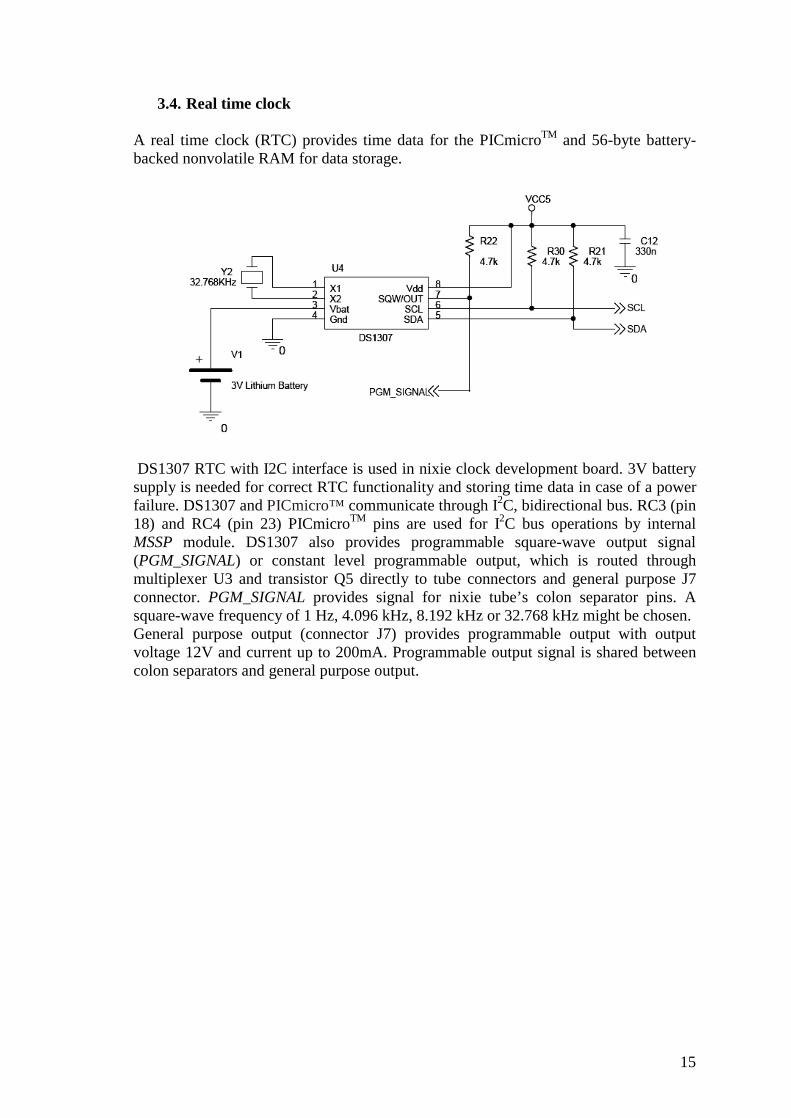
3.4. Real time clock A real time clock (RTC) provides time data for the PICmicroTM and 56-byte battery-backed nonvolatile RAM for data storage.
DS1307 RTC with I2C interface is used in nixie clock development board. 3V battery supply is needed for correct RTC functionality and storing time data in case of a power failure. DS1307 and PICmicro™ communicate through I2C, bidirectional bus. RC3 (pin 18) and RC4 (pin 23) PICmicroTM pins are used for I2C bus operations by internal MSSP module. DS1307 also provides programmable square-wave output signal (PGM_SIGNAL) or constant level programmable output, which is routed through multiplexer U3 and transistor Q5 directly to tube connectors and general purpose J7 connector. PGM_SIGNAL provides signal for nixie tube’s colon separator pins. A square-wave frequency of 1 Hz, 4.096 kHz, 8.192 kHz or 32.768 kHz might be chosen. General purpose output (connector J7) provides programmable output with output voltage 12V and current up to 200mA. Programmable output signal is shared between colon separators and general purpose output.

16
3.5. Temperature sensor The board is equipped with high precision digital thermometer DS1820.
It measures temperature in range from –55°C to +125°C (–67°F to +257°F). Temperature is converted to digital word in several milliseconds and read from the DS1820 over a 1–WireTM interface, so that only one wire is connected to PICmicroTM RC5 ( pin 24).
3.6. Photo sensor and buzzer The board is equipped with photo resistor for measuring environment illumination and buzzer for sound generation.
Analogue signal from photo resistor is routed to the PICmicroTM RA0 (pin 2) analogue input. An internal PICmicroTM Analog-to-Digital module is used to convert analog singal to digital. Onboard buzzer is connected to the PICmicroTM RA0 (pin 2) via decoupling capacitor C15. When configured as output, RA0 pin generates sound signal for buzzer. It is recommended to measure illumination not sooner than 1s after pin direction change.
17
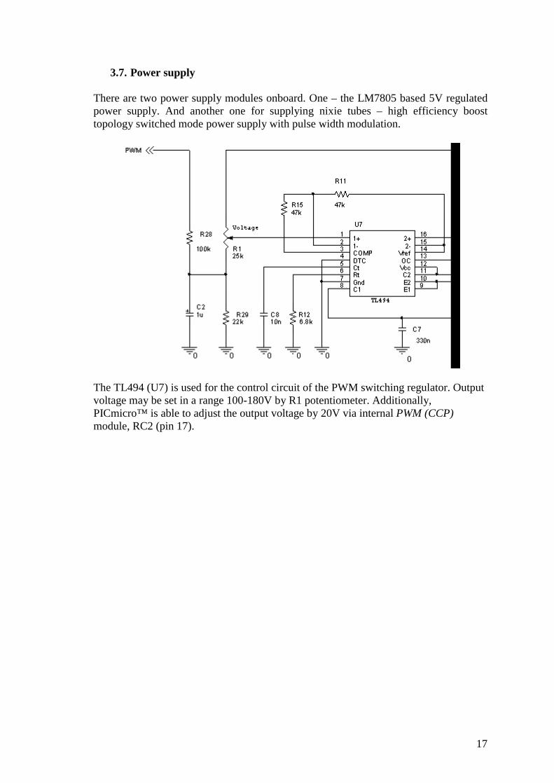
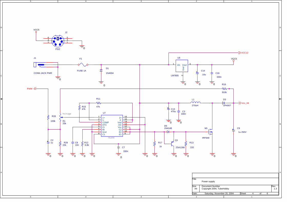
3.7. Power supply
There are two power supply modules onboard. One – the LM7805 based 5V regulated power supply. And another one for supplying nixie tubes – high efficiency boost topology switched mode power supply with pulse width modulation.
The TL494 (U7) is used for the control circuit of the PWM switching regulator. Output voltage may be set in a range 100-180V by R1 potentiometer. Additionally, PICmicro™ is able to adjust the output voltage by 20V via internal PWM (CCP) module, RC2 (pin 17).
18
3.8. Buttons The board has 2 control buttons, SW1 and SW2.
5
SW1
4
SW2
SW2
3
J6
VCC5
SW1
R24
220
J5
0
R312.2k
R26
220
0
R322.2k
6
Onboard buttons SW1 and SW2 are connected to the PICmicroTM RC0 (pin 15) and RC1 (pin 16) respectively. An R24 and R26 resistor protects PICmicroTM port from accidental port direction mis-setting. It is possible to connect external control buttons to J5 and J6 connectors.
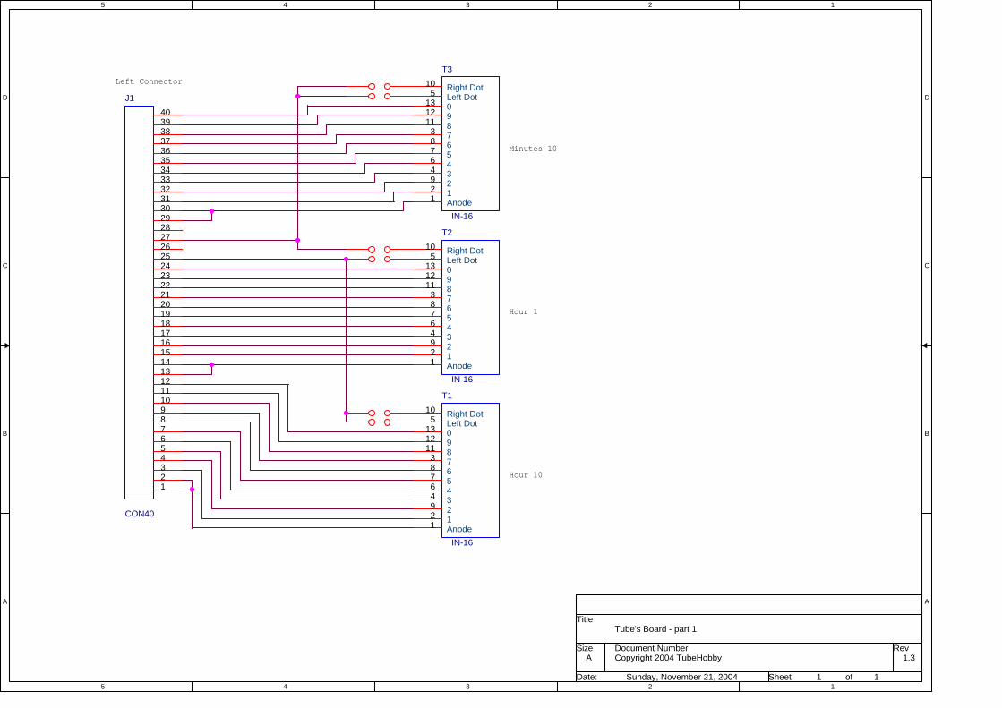
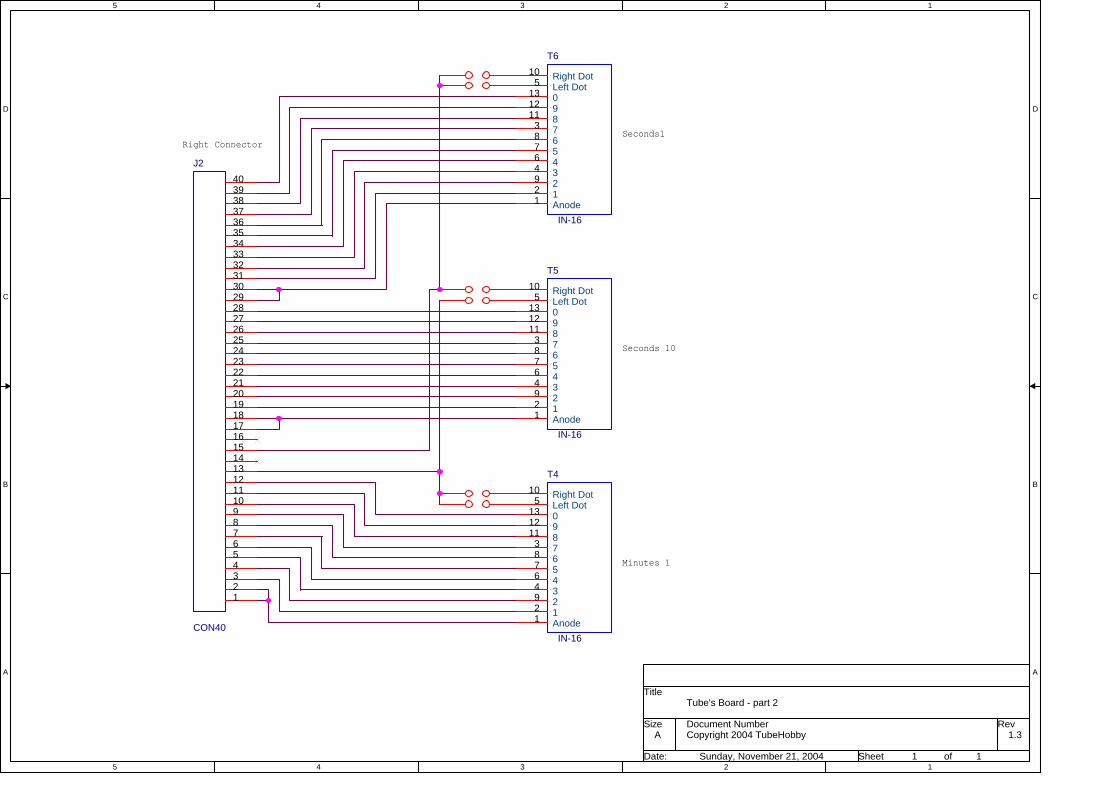
3.9. Tube’s board A small PCB is included with “Nixie Clock Development Board v1.3” which carry 6 nixie tubes. Two 40-pin receptacle type connectors may be connected directly to the development board.
There are two solderable jumpers across each tube on the bottom side of tube’s board, which connects appropriate dots of the tube to the programmable output. Recommended anode current for the IN-16 nixie tubes is 2 mA. It is easy to measure voltage across the anode (limiting) resistor and then calculate current.

19
4. Typical performance characteristics
4.1. Nixie Clock Development Board with 6 x IN-16 tubes, 10K anode resistors
Current consumption
0.0
0.5
1.0
1.5
2.0
2.5
3.0
3.5
0 0.2 0.4 0.6
Input current at 12V [A]
Ano
de c
urre
nt [m
A]
Output VA characteristic
0.0
0.5
1.0
1.5
2.0
2.5
3.0
3.5
120 130 140 150 160 170 180 190
Output voltage [V]
Ano
de c
urre
nt [m
A]
4.2. Nixie Clock Development Board with 6 x IN-18 tubes, 10K anode resistors
Current consumption
0.0
0.5
1.0
1.5
2.0
2.5
3.0
3.5
4.0
0 0.2 0.4 0.6
Input current at 12V [A]
Ano
de c
urre
nt [m
A]
Output VA characteristic
0.0
0.5
1.0
1.5
2.0
2.5
3.0
3.5
4.0
120 130 140 150 160 170 180 190
Output voltage [V]
Ano
de c
urre
nt [m
A]
20
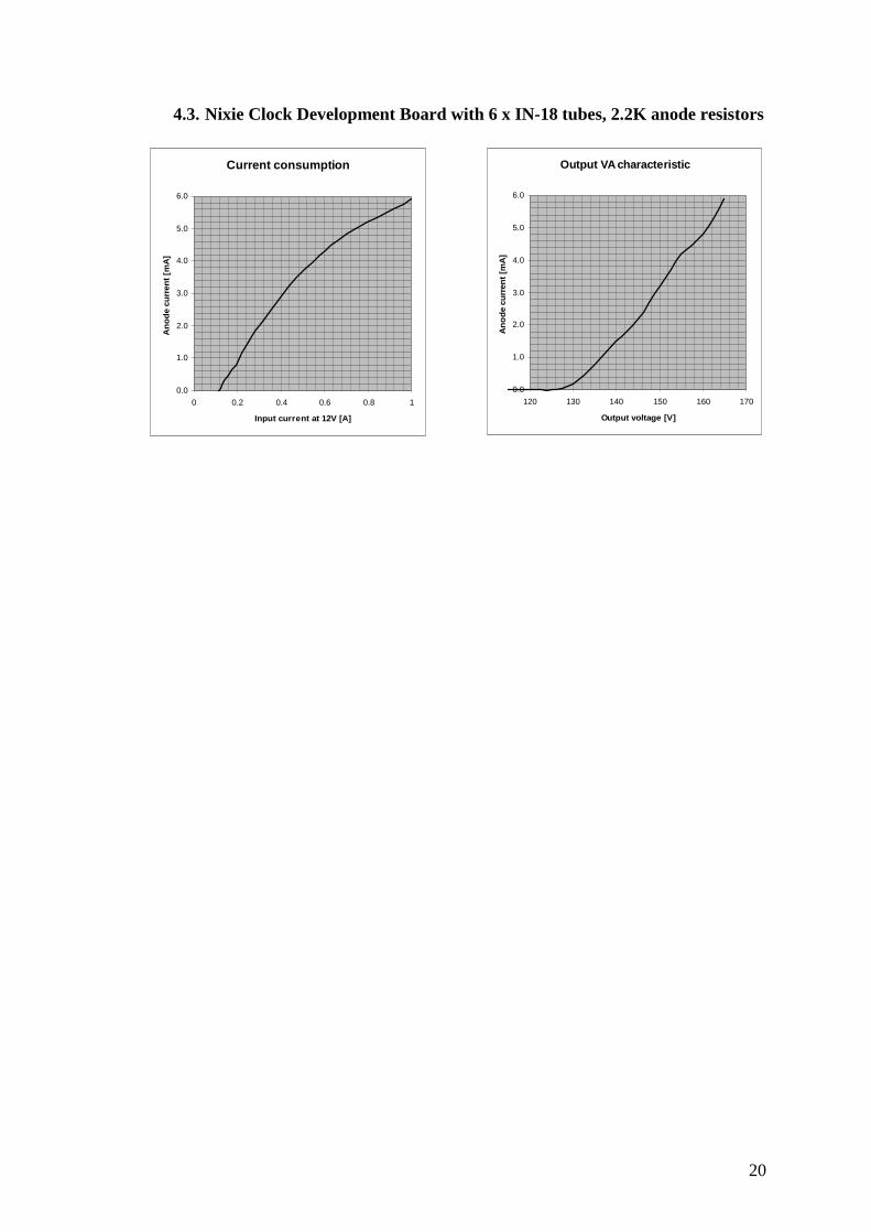
4.3. Nixie Clock Development Board with 6 x IN-18 tubes, 2.2K anode resistors
Current consumption
0.0
1.0
2.0
3.0
4.0
5.0
6.0
0 0.2 0.4 0.6 0.8 1
Input current at 12V [A]
Ano
de c
urre
nt [m
A]
Output VA characteristic
0.0
1.0
2.0
3.0
4.0
5.0
6.0
120 130 140 150 160 170
Output voltage [V]
Ano
de c
urre
nt [m
A]

5
5
4
4
3
3
2
2
1
1
D D
C C
B B
A A
Copyright 2004, TubeHobby 1.3
High voltage drivers - part 2
A4
1 6Saturday, November 20, 2004
Title
Size Document Number Rev
Date: Sheet of
SEC_HI_NIB_A0
SEC_HI_NIB_A1
SEC_HI_NIB_A2
SEC_HI_NIB_A3
SEC_LO_NIB_A0
SEC_LO_NIB_A1
SEC_LO_NIB_A2
SEC_LO_NIB_A3
Vcc_HI
Vcc_HI
MIN_LO_NIB_A2
MIN_LO_NIB_A0
Vcc_HI
MIN_LO_NIB_A3
MIN_LO_NIB_A1
Switch
0
0
VCC5
VCC5
0
VCC5
U14
K155ID1
16
15891314111012
3674
512 Y0
Y1Y2Y3Y4Y5Y6Y7Y8Y9
A0A1A2A3
VddGnd
J9
CON40 Plug
123456789
10111213141516171819202122232425262728293031323334353637383940
R40
10kU12
K155ID1
16
15891314111012
3674
512 Y0
Y1Y2Y3Y4Y5Y6Y7Y8Y9
A0A1A2A3
VddGnd
R41
10k
R42
10k
R38
22k
U13
K155ID1
16
15891314111012
3674
512 Y0
Y1Y2Y3Y4Y5Y6Y7Y8Y9
A0A1A2A3
VddGnd
R39
22k
5
5
4
4
3
3
2
2
1
1
D D
C C
B B
A A
Copyright 2004, TubeHobby 1.3
High voltage drivers - part 1
A4
2 6Saturday, November 20, 2004
Title
Size Document Number Rev
Date: Sheet of
HOU_LO_NIB_A1
HOU_LO_NIB_A0
HOU_LO_NIB_A3
Vcc_HI
HOU_HI_NIB_A3
HOU_LO_NIB_A2
HOU_HI_NIB_A2
Vcc_HI
HOU_HI_NIB_A1
HOU_HI_NIB_A0
MIN_HI_NIB_A0
MIN_HI_NIB_A3
Vcc_HI
MIN_HI_NIB_A2
MIN_HI_NIB_A1
Switch
0
0
VCC5
VCC5
0
VCC5
R36
22k
R37
22k
J8
CON40 Plug
123456789
10111213141516171819202122232425262728293031323334353637383940
R34
10k
U10
K155ID1
16
15891314111012
3674
512 Y0
Y1Y2Y3Y4Y5Y6Y7Y8Y9
A0A1A2A3
VddGnd
U11
K155ID1
16
15891314111012
3674
512 Y0
Y1Y2Y3Y4Y5Y6Y7Y8Y9
A0A1A2A3
VddGnd
R33
10k
U9
K155ID1
16
15891314111012
3674
512 Y0
Y1Y2Y3Y4Y5Y6Y7Y8Y9
A0A1A2A3
VddGnd
R35
10k
5
5
4
4
3
3
2
2
1
1
D D
C C
B B
A A
U8
Copyright 2004, TubeHobby 1.3
Microcontroller unit
A4
3 6Saturday, November 20, 2004
Title
Size Document Number Rev
Date: Sheet of
RB7
RB6
SEC_HI_NIB_A1
SEC_HI_NIB_A0
SEC_LO_NIB_A3
SEC_LO_NIB_A2
SEC_LO_NIB_A1
MIN_HI_NIB_A3
MIN_HI_NIB_A2
MIN_HI_NIB_A1
MIN_HI_NIB_A0
MIN_LO_NIB_A3
MIN_LO_NIB_A2
MIN_LO_NIB_A1
MIN_LO_NIB_A0
HOU_HI_NIB_A3
HOU_LO_NIB_A2
HOU_LO_NIB_A1
HOU_HI_NIB_A0
HOU_HI_NIB_A1
HOU_LO_NIB_A0
HOU_LO_NIB_A3
HOU_HI_NIB_A2
SEC_LO_NIB_A0
PWM
SDA
SW1
TX
Light
SCL
SW2
1W
RX
MCLR0
0 0
VCC5
0
VCC5
R27
4.7k
C10330n
Y1
20MHzC11
22p
C17
22p PIC16F877
234567
3334353637383940
2625242318171615
3029282722212019
8910
1132123113141
RA0/AN0RA1/AN1RA2/AN2/Vref-RA3/AN3/Vref+RA4/T0CKIRA5/AN4/SS
RB0/INTRB1RB2
RB3/PGMRB4RB5
RB6/PGCRB7/PGD
RC7/RX/DTRC6/TX/CKRC5/SDORC4/SDI/SDARC3/SCK/SCLRC2/CCP1RC1/T1OSI/CCP2RC0/T1OSO/T1CKI
RD7/PSP7RD6/PSP6RD5/PSP5RD4/PSP4RD3/PSP3RD2/PSP2RD1/PSP1RD0/PSP0
RE0/RD/AN5RE1/WR/AN6RE2/CS/AN7
Vdd1Vdd2Vss1Vss2OSC1/CLKINOSC2/CLKOUTMCLR/Vpp/THV
RC3RC4
RB7RB6RB5RB4RB3RB2RB1RB0
RD7RD6RD5RD4RD3RD2RD1RD0
RE2RE1
RC0RC1RC2
RC5
RB7
RB6
RB5
RB4
RB3
RB2
RB1
RB0
RD7
RD6
RD5
RD4
RD3
RD2
RD1
RD0
RA5
RE2
RE1
RE0
RA4
RA3
RA2
RA1
RA4RA3RA2RA1RA0
RC2
RC1
RA0
RC0
RC5
RC3
RC4
RC6
RC6RC7
RC7
RE0
RA5
5
5
4
4
3
3
2
2
1
1
D D
C C
B B
A A
Voltage
Copyright 2004, TubeHobby 1.3
Power supply
A4
4 6Saturday, November 20, 2004
Title
Size Document Number Rev
Date: Sheet of
Vcc_HI
PWM
VCC12
000 0 0 0 00 0
00
000
0
VCC5
0
VCC5
0
0
0 0
D51N4148
R28
100k
C13470u
R1547k
Q1
2SA1266
R17
1k
C21u R12
6.8k
L1
270uH
R11
47k
J1
CONN JACK PWR
J2
PS/2
642
531
R13
220
C810n
M1
IRF640
R125k
C9
1u 250V
TL494
U7
12345678 9
101112131415161+
1-COMPDTCCtRtGndC1 E1
E2C2
VccOC
Vref2-2+
D1
1N4004
U6
LM7805
1
2
3Vin
Gnd
Vout
D3
UF4007
C14
10u
R2922k
C16
330n
C7
330n
C3330n
F1
FUSE 1A
R16
910k

5
5
4
4
3
3
2
2
1
1
D D
C C
B B
A A
+
4 3
56
1
2
Copyright 2004, TubeHobby 1.3
Peripheral
A4
5 6Saturday, November 20, 2004
Title
Size Document Number Rev
Date: Sheet of
SCL
SDA1W
Light
SW2
SW1
TX
RX
Switch
VCC12
PGM_OUT
PGM_SIGNAL
VCC5
0
0
0
VCC5 VCC5
0
0 0
VCC5
0 0
VCC5VCC5
00
00
R26
220
C41u
C1
1u
J7
C15
330n
C6
1u
U4
DS1307
1234
8765
X1X2VbatGnd
VddSQW/OUT
SCLSDA
R24
220
R22
4.7kR21
4.7k
U1
MAX232
12345678 9
10111213141516C1+
Vs+C1-C2+C2-Vs-T2OutR2In R2Out
T2InT1In
R1OutR1In
T1OutGndVcc
J5
B1
AL-60P01
C51u
R234.7k
R19
47k
+ V1
3V Lithium Battery
R18
MPY7P
SW2
Q5MPSA42
C12330n
R322.2k
Y232.768KHz
R304.7k
U5
DS1820
123
GndDQ
Vdd
J3
CONNECTOR DB9
594837261
SW1
J6
R312.2k
5
5
4
4
3
3
2
2
1
1
D D
C C
B B
A A
RESET
Copyright 2004, TubeHobby 1.3
Parallel port programmer
A4
6 6Saturday, November 20, 2004
Title
Size Document Number Rev
Date: Sheet of
RB6
RB7
SEC_HI_NIB_A2
SEC_HI_NIB_A3
VCC12
MCLR
PGM_SIGNAL
PGM_OUT
0
0
0
VCC5
0
0
VCC5
0
0
0 0 0 0 0
0
VCC5
0
R5
22kR8
4.7k
R747k
Q42N2222
R25
220
U2
4050
12345678 9
10111213141516Vcc
1Y1A2Y2A3Y3AGnd 4A
4Y5A5Y
N C6A6YNC
R20
4.7k
R6470
D4
LED
R14
22k
R2
22k
Q2
2SA1266
J4
CONNECTOR DB25
13251224112310229218207196185174163152141
SW3
R3
22k
R94.7k
Q32N2222
D212V Zener
R4
22k
U3
4053
12345678 9
101112131415162Y1
2Y03Y13Z3Y0~EVeeGnd S3
S2S1
1Y01Y1
1Z2Z
Vcc
R10220
5
5
4
4
3
3
2
2
1
1
D D
C C
B B
A A
Hour 10
Hour 1
Minutes 10
Left Connector
Copyright 2004 TubeHobby 1.3
Tube's Board - part 1
A
1 1Sunday, November 21, 2004
Title
Size Document Number Rev
Date: Sheet of
J1
CON40
12345678910111213141516171819202122232425262728293031323334353637383940
T3
IN-16
12
3
4
5
678
9
10
111213
Anode1
7
3
Left Dot
456
2
Right Dot
890
T1
IN-16
12
3
4
5
678
9
10
111213
Anode1
7
3
Left Dot
456
2
Right Dot
890
T2
IN-16
12
3
4
5
678
9
10
111213
Anode1
7
3
Left Dot
456
2
Right Dot
890
5
5
4
4
3
3
2
2
1
1
D D
C C
B B
A A
Minutes 1
Seconds 10
Seconds1Right Connector
Copyright 2004 TubeHobby 1.3
Tube's Board - part 2
A
1 1Sunday, November 21, 2004
Title
Size Document Number Rev
Date: Sheet of
J2
CON40
12345678910111213141516171819202122232425262728293031323334353637383940
T4
IN-16
12
3
4
5
678
9
10
111213
Anode1
7
3
Left Dot
456
2
Right Dot
890
T6
IN-16
12
3
4
5
678
9
10
111213
Anode1
7
3
Left Dot
456
2
Right Dot
890
T5
IN-16
12
3
4
5
678
9
10
111213
Anode1
7
3
Left Dot
456
2
Right Dot
890