Embed Size (px)
Citation preview

Nat.Lab. NL-UR 816/98
Date of issue: ASAP
New 1/f noise model inMOS Model 9, level 903
A.J. Scholten and D.B.M. Klaassen
Company restrictedc Philips Electronics 1998

816/98 Company restricted
Authors' address data: A.J. Scholten WAG01; scholtn@prle
D.B.M. Klaassen WAG13; klaassen@prle
c Philips Electronics N.V. 1998
All rights are reserved. Reproduction in whole or in part is
prohibited without the written consent of the copyright owner.
iic Philips Electronics N.V. 1998

Company restricted 816/98
NL-UR: 816/98
Title: New 1/f noise model in
MOS Model 9, level 903
Author(s): A.J. Scholten and D.B.M. Klaassen
Part of project: Compact modelling
Customer: Philips Semiconductors
Keywords: Mos Model 9; 1/f noise; parameter extraction; level 903
Abstract: The 1=f noise model in MOS Model 9, level 902, fails to
describe the VGS dependence of the input-referred noise, ob-
served in experiments. A new 1=f noise model has been
selected, and implemented in MOS Model 9, level 903. In
this report, its physical background is explained. Moreover,
noise measurements and noise parameter extraction on C075
are described. It is shown that the amount of 1=f noise in
HCMOS6 and C075 is comparable. The geometrical scaling
rules of the noise model have been veri�ed experimentally
for both n- and p-channel MOSFETs. Moreover, it is shown
that the new model gives an improved description of the
noise in both linear and saturation regime. The new model
is available in PSTAR 3.7 as MOS Model 9, level 903. It will
be available in HSPICE 98.2.1 (August '98), and in SPEC-
TRE 4.4.3 (November '98).
Conclusions: MOS Model 9, level 903, contains a new 1=f noise model.
� The model describes the bias dependence of the 1=f
noise very well.
� The geometrical scaling rules of the model have been
veri�ed on C075 silicon.
� The following set of parameters is recommended for
C075:
N-channels P-channels
NFAR (V�1m
�4) 39:8 � 10
2315:4 � 10
23
NFMOD=1 NFBR (V�1m
�2) 3:24 � 10
80:179 � 10
8
NFCR (V�1) 0 0:148 � 10
�7
NFMOD=0 NFR (V2) 19:91 � 10
�115:81 � 10
�11
c Philips Electronics N.V. 1998 iii
816/98 Company restricted
ivc Philips Electronics N.V. 1998

Company restricted 816/98
Contents
1 Introduction 1
2 Low-frequency noise in MOSFETS 3
2.1 Low-frequency noise spectrum of a MOSFET . . . . . . . . . . . . . . 3
2.2 Output noise current and input-referred noise voltage sources . . . . . 4
2.3 The 1=f noise model in MOS Model 902 and its limitations . . . . . . 5
3 New 1=f noise model 9
3.1 Qualitative description . . . . . . . . . . . . . . . . . . . . . . . . . . 9
3.2 MOS Model 9, level 903 1=f noise model . . . . . . . . . . . . . . . . 10
3.3 Relation with the BSIM3v3 model . . . . . . . . . . . . . . . . . . . . 12
4 Noise measurements on C075 13
4.1 Test structures . . . . . . . . . . . . . . . . . . . . . . . . . . . . . . 13
4.2 DC-characterization . . . . . . . . . . . . . . . . . . . . . . . . . . . . 14
4.3 Experimental setup and data handling . . . . . . . . . . . . . . . . . 16
4.4 Sample-to-sample spread and comparison with HCMOS6 . . . . . . . 18
4.5 Veri�cation of the geometrical scaling rules . . . . . . . . . . . . . . . 20
4.6 Parameter extraction . . . . . . . . . . . . . . . . . . . . . . . . . . . 22
4.7 Improved modelling accuracy in the linear regime . . . . . . . . . . . 23
5 Conclusion 25
A Noise in MOSFETs: theory 27
A.1 General method for noise calculations in MOSFETs . . . . . . . . . . 27
A.2 Application of Hooge's law to a MOSFET . . . . . . . . . . . . . . . 29
B The level 903 1=f noise model 31
B.1 Derivation of the model by Hung et al. . . . . . . . . . . . . . . . . . 31
B.2 Rewriting Hung's model in MOS Model 9 terms . . . . . . . . . . . . 33
B.3 The transition between weak and strong inversion . . . . . . . . . . . 36
B.4 The value of N� . . . . . . . . . . . . . . . . . . . . . . . . . . . . . . 37
B.5 Scaling rules . . . . . . . . . . . . . . . . . . . . . . . . . . . . . . . . 37
B.6 Simpli�ed model and physical interpretation of the parameters . . . . 38
B.7 Hooge's law . . . . . . . . . . . . . . . . . . . . . . . . . . . . . . . . 39
C List of used symbols 41
References 45
Distribution
c Philips Electronics N.V. 1998 v

816/98 Company restricted
vic Philips Electronics N.V. 1998
Company restricted 816/98
1 Introduction
The modelling of low-frequency noise, and 1=f noise in particular, is becoming
increasingly important. Evidently, 1=f noise limits the performance of low-frequency
circuits. Moreover, in high-frequency and RF applications, such as phase-locked
loops and voltage-controlled oscillators, 1=f noise plays an important role as well.
In the case of an oscillator, for instance, the low-frequency noise may mix with the
oscillation frequency, resulting in an unwanted increase of the signal bandwidth.
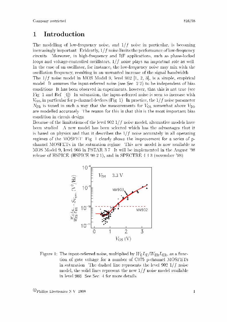
The 1=f noise model in MOS Model 9, level 902 [1, 2, 3], is a simple, empirical
model. It assumes the input-referred noise (see Sec. 2.2) to be independent of bias
conditions. It has been observed in experiments, however, that this is not true (see
Fig. 1 and Ref. [4]). In saturation, the input-referred noise is seen to increase with
VGS, in particular for p-channel devices (Fig. 1). In practice, the 1=f noise parameter
NFR is tuned in such a way that the measurements for VGS somewhat above VTO
are modelled accurately. The reason for this is that this is the most important bias
condition in circuit design.
Because of the limitations of the level 902 1=f noise model, alternative models have
been studied. A new model has been selected which has the advantages that it
is based on physics and that it describes the 1=f noise accurately in all operating
regimes of the MOSFET. Fig. 1 clearly shows the improvement for a series of p-
channel MOSFETs in the saturation regime. This new model is now available as
MOS Model 9, level 903 in PSTAR 3.7. It will be implemented in the August '98
release of HSPICE (HSPICE 98.2.1), and in SPECTRE 4.4.3 (november '98).
W
E�
LE
W
ER�
LER
�
SVgate(V
2/Hz)
VGS (V)
VDS = 3:3 V
Figure 1: The input-referred noise, multiplied by WELE=WERLER, as a func-
tion of gate voltage for a number of C075 p-channel MOSFETs
in saturation. The dashed line represents the level 902 1=f noise
model, the solid lines represent the new 1=f noise model available
in level 903. See Sec. 4 for more details.
c Philips Electronics N.V. 1998 1

816/98 Company restricted
This report is organized as follows: In chapter 2, we will introduce the reader to the
subject of low-frequency noise in MOSFETs. For reasons of tractability, mathemat-
ical derivations are postponed to appendix A.
Then, in chapter 3 the physical background of the new 1=f noise model will be
explained qualitatively. The derivation of the model is elucidated in appendix B.
In chapter 4, the measurements are described that were performed on C075 silicon.
In that chapter we will show that the new 1=f noise model is capable of describing the
measurement results accurately in all operating regimes of the MOSFET. Moreover,
the geometrical scaling rules are veri�ed on a set of 11 geometries. The extraction
of the noise parameters is discussed.
Finally, in chapter 5, this work is summarized and the conclusions are presented. A
list of all the symbols, used throughout this report, is given in appendix C.
2c Philips Electronics N.V. 1998
Company restricted 816/98
2 Low-frequency noise in MOSFETS
2.1 Low-frequency noise spectrum of a MOSFET
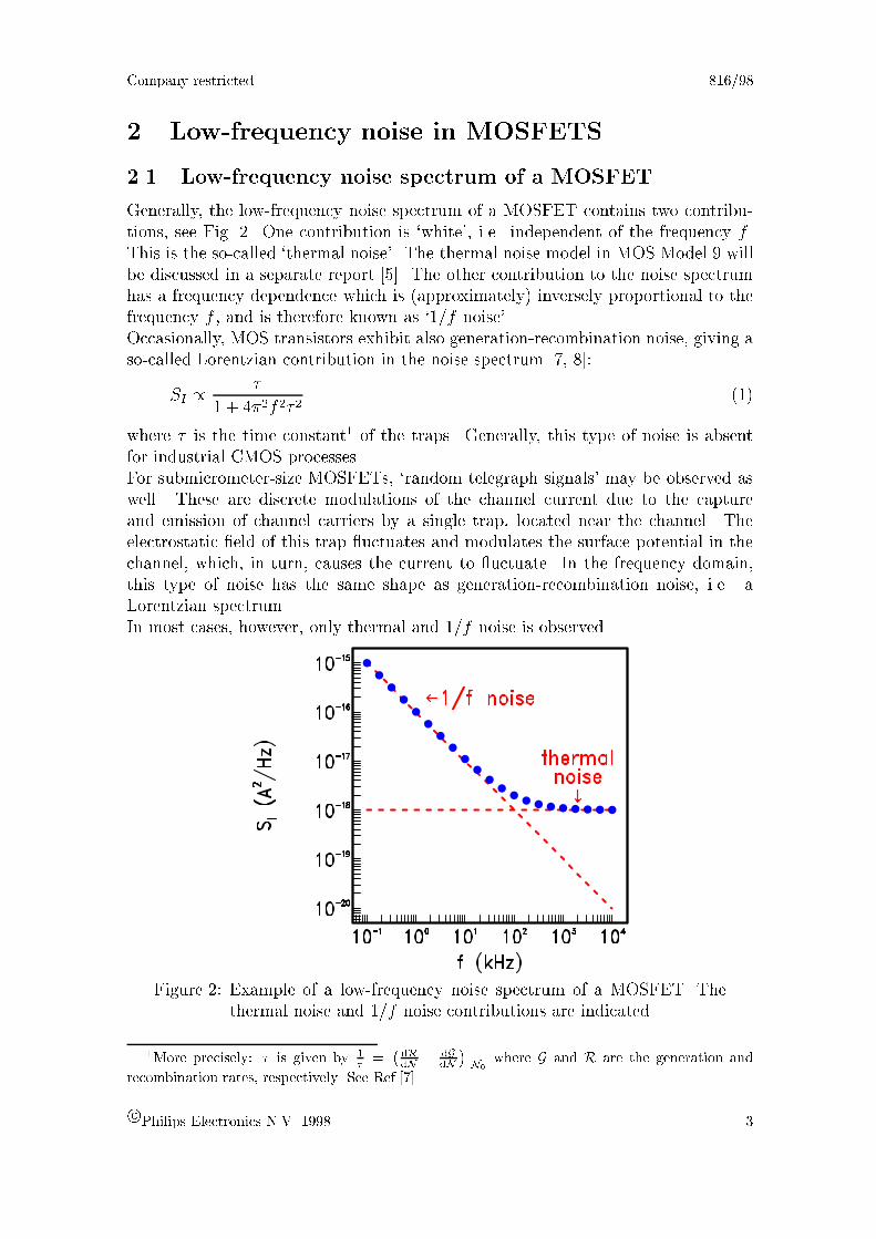
Generally, the low-frequency noise spectrum of a MOSFET contains two contribu-
tions, see Fig. 2. One contribution is `white', i.e. independent of the frequency f .
This is the so-called `thermal noise'. The thermal noise model in MOS Model 9 will
be discussed in a separate report [5]. The other contribution to the noise spectrum
has a frequency dependence which is (approximately) inversely proportional to the
frequency f , and is therefore known as `1=f noise'.
Occasionally, MOS transistors exhibit also generation-recombination noise, giving a
so-called Lorentzian contribution in the noise spectrum [7, 8]:
SI /�
1 + 4�2f 2� 2(1)
where � is the time constant1 of the traps. Generally, this type of noise is absent
for industrial CMOS processes.
For submicrometer-size MOSFETs, `random telegraph signals' may be observed as
well. These are discrete modulations of the channel current due to the capture
and emission of channel carriers by a single trap, located near the channel. The
electrostatic �eld of this trap uctuates and modulates the surface potential in the
channel, which, in turn, causes the current to uctuate. In the frequency domain,
this type of noise has the same shape as generation-recombination noise, i.e. a
Lorentzian spectrum.
In most cases, however, only thermal and 1=f noise is observed.
Figure 2: Example of a low-frequency noise spectrum of a MOSFET. The
thermal noise and 1=f noise contributions are indicated.
1More precisely: � is given by 1
�=
�dRdN
� dGdN
���N0
where G and R are the generation and
recombination rates, respectively. See Ref.[7]
c Philips Electronics N.V. 1998 3
816/98 Company restricted
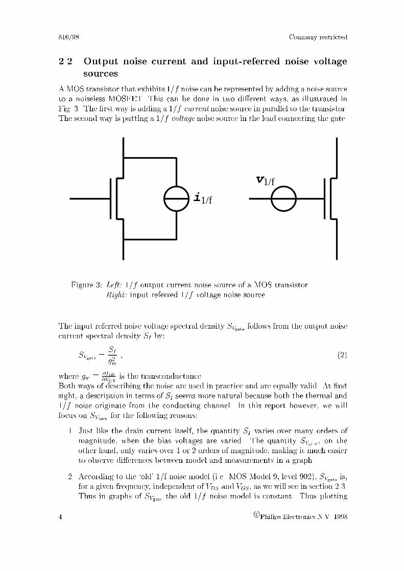
2.2 Output noise current and input-referred noise voltage
sources
AMOS transistor that exhibits 1=f noise can be represented by adding a noise source
to a noiseless MOSFET. This can be done in two di�erent ways, as illustrated in
Fig. 3. The �rst way is adding a 1=f current noise source in parallel to the transistor.
The second way is putting a 1=f voltage noise source in the lead connecting the gate.
v1/f
i1/f
Figure 3: Left: 1=f output current noise source of a MOS transistor.
Right: input referred 1=f voltage noise source.
The input referred noise voltage spectral density SVgate follows from the output noise
current spectral density SI by:
SVgate =SI
g2m
; (2)
where gm �@IDS@VGS
is the transconductance.
Both ways of describing the noise are used in practice and are equally valid. At �rst
sight, a description in terms of SI seems more natural because both the thermal and
1=f noise originate from the conducting channel. In this report however, we will
focus on SVgate for the following reasons:
1. Just like the drain current itself, the quantity SI varies over many orders of
magnitude, when the bias voltages are varied. The quantity SVgate , on the
other hand, only varies over 1 or 2 orders of magnitude, making it much easier
to observe di�erences between model and measurements in a graph.
2. According to the `old' 1/f noise model (i.e. MOS Model 9, level 902), SVgate is,
for a given frequency, independent of VDS and VGS, as we will see in section 2.3.
Thus in graphs of SVgate the old 1=f noise model is constant. Thus plotting
4c Philips Electronics N.V. 1998
Company restricted 816/98
SVgate makes the shortcomings of the old 1=f noise model and di�erences with
the new model clearly visible.
3. In circuit analysis, the quantity SVgate is more relevant than SI . This is because
the noise �gure F , i.e. the ratio of signal-to-noise power ratios at the input
and the output of the device, is directly related to SVgate by [4, 6]
F = 1 +SVgate
SV;input(3)
2.3 The 1=f noise model in MOS Model 902 and its limita-
tions
A large variety of explanations for 1=f noise is found in the literature, which can be
divided in two major categories. One is the McWorther trapping theory, the other
the mobility uctuation theory of Hooge. The noise model presented in this report,
in fact, is a combination of these two models.
A simple, but already very useful formula for 1=f noise in a MOSFET is obtained if
one assumes the empirical \Hooge's law" to be valid microscopically. This leads to
SI = �H �q�e�IDSVDS
fL2(4)
The derivation of this formula is found in Sec. A.2. The major drawback of this
formula for compact modelling is that it underestimates the measurements consid-
erably near VTO, which is the most important bias condition for circuit simulation.
Therefore, MOS Model 9, level 902, contains another noise model, which is purely
empirical. The MM902 expression for S , the icker noise contribution in the noise
current spectral density, reads:
S = NF �g2m
f(5)
Here, S is the icker noise contribution in the noise current spectral density. In
terms of input referred noise the above equation simpli�es to:
SVgate =NF
f(6)
The geometrical scaling rule for NF reads:
NF = NFR �WERLER
WELE
(7)
Note that there is no explicit temperature scaling rule. There is only an implicit
temperature dependence of the output current noise via gm.
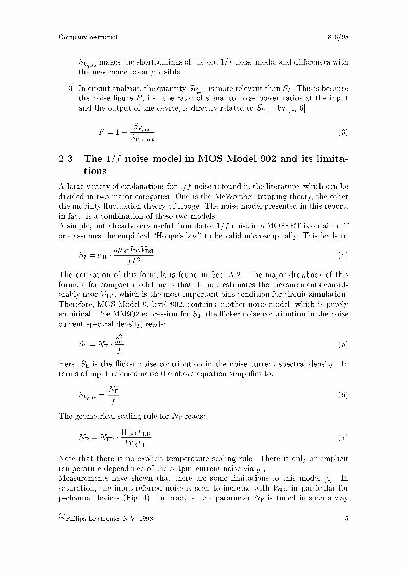
Measurements have shown that there are some limitations to this model [4]. In
saturation, the input-referred noise is seen to increase with VGS, in particular for
p-channel devices (Fig. 4). In practice, the parameter NF is tuned in such a way
c Philips Electronics N.V. 1998 5

816/98 Company restricted
that the measurements for VGS somewhat above VTO are modelled accurately (see
Fig. 4)., the reason being that this is the most important bias condition in circuit
design.
Because of the limitations of the level 902 1=f noise model, described above, alterna-
tive 1=f noise models have been studied. A new 1=f noise model has been selected
and incorporated in MOS Model 9. This new model is available in MOS Model 9
level 903. It can be selected by setting the switch NFMOD to 1. By default, this
switch is set to 0, which selects the level 902 1=f noise model. This construction
makes the level 903 model backwards compatible, i.e. old parameter sets can still
be used in level 903, yielding the same results as before.
MOS Model 9, level 903, is already available in PSTAR 3.7, and it will be imple-
mented in HSPICE 98.2.1 (August '98), and in SPECTRE 4.4.3 (November '98).
6c Philips Electronics N.V. 1998
Company restricted 816/98
Figure 4: Measurements (from Ref. [4]) of the input-referred 1=f noise as
a function of gate voltage for MOSFETs in saturation, for the
C200, C150 and C100 processes. Di�erent grey scales correspond
to di�erent, nominally identical, devices. Solid lines represent the
MM902 model, using NFR from the design manuals. Left: n-
channels. Right: p-channels.c Philips Electronics N.V. 1998 7

816/98 Company restricted
8c Philips Electronics N.V. 1998
Company restricted 816/98
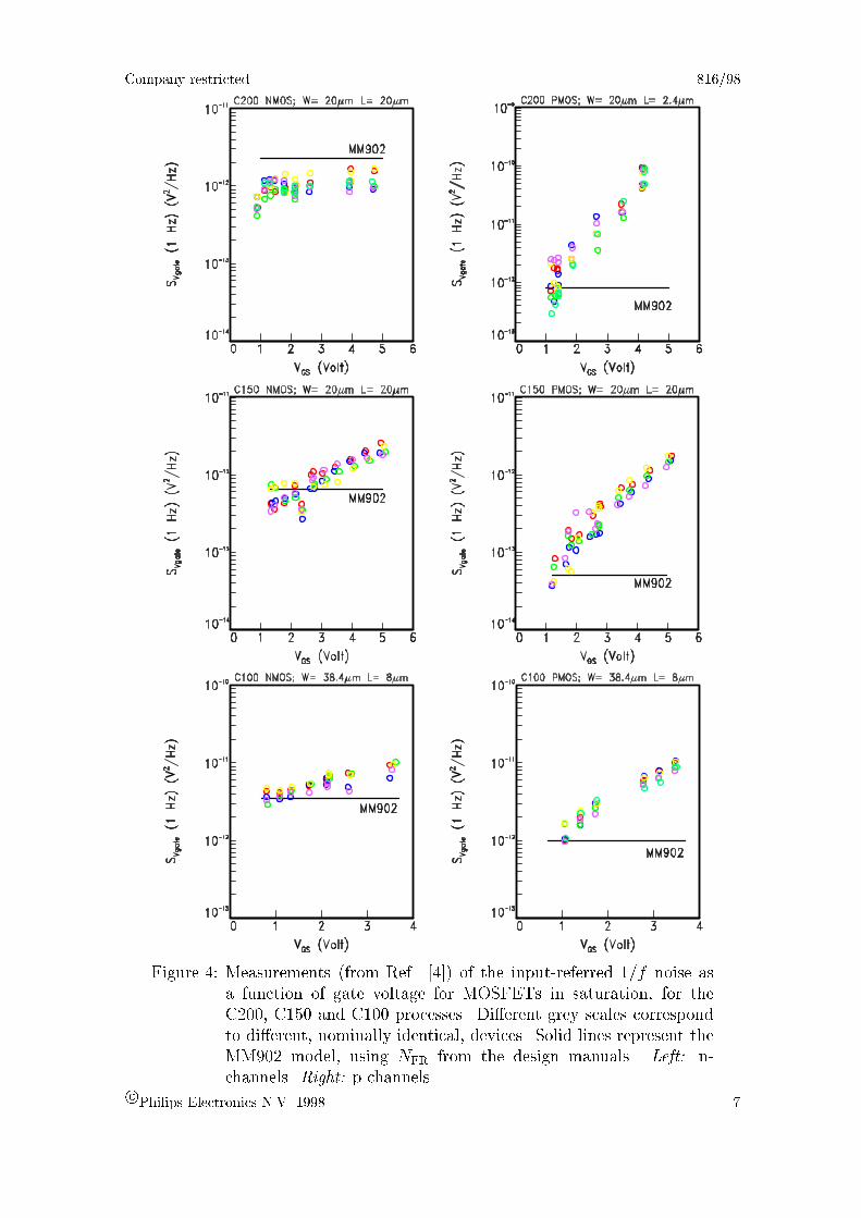
3 New 1=f noise model
3.1 Qualitative description
The new 1=f noise model is based on two papers by K.K. Hung et al. [9, 10]. It as-
sumes trapping and detrapping of charge carriers in the gate oxide to be responsible
for the observed 1=f noise. This is illustrated in Fig. 5.
substrate
gate
drainsource
gate oxide
Figure 5: Physical background of the new 1=f noise model.
The trapping and detrapping processes causes the number of carriers to uctuate,
which of course leads to uctuations in the current. Moreover, the trapping of a
charge carrier leads to a change of the electric �eld experienced by the charge carriers
in the inversion layer. In other words, not only the number of carriers, but also the
mobility uctuates. Evidently, the two e�ects are correlated, which is taken into
account in the model.
The most characteristic feature of 1=f noise is, of course, its spectrum. How is
this spectrum explained in the new model? Let us �rst assume that we have a
single trap in the oxide, characterized by a single time constant � . In this case
\random telegraph signals" (RTS), may be observed in the time domain, i.e. the
measured current switches back and forth between two (or more) discrete levels. In
the frequency domain, this leads to a Lorentzian noise spectrum:
�
1 + 4�2f 2� 2(8)
The type of uctuations described here are indeed sometimes observed for very-
small sized MOSFETs, where a single, strategically located trap may dominate the
uctuations.
For larger MOSFETs, however, there is usually more than one trap and thus a
distribution of trapping sites in the oxide. This leads to a distribution of trapping
c Philips Electronics N.V. 1998 9

816/98 Company restricted
times
� = �0(E) � exp( ox � z) (9)
where z is the distance between traps and interface, ox � 1 �A�1 is the attenuation
coe�cient of the electron wave function in the gate oxide, and �0(E) is the time
constant of traps located at the Si/SiO2 interface (z = 0). It is the integration
over z that leads to a 1=f spectrum, if the trap distribution is spatially uniform, in
particular near the interface. This is illustrated in Fig. 6. Deviations from `true'
1=f noise, e.g. 1=f noise, can be understood in terms of deviations from a spatially
uniform distribution of traps. However, no systematic trends of this exponent are
known as a function of bias conditions or geometry. Therefore, it makes no sense to
take these deviations from `true' 1=f noise into account in compact modelling.
Figure 6: The addition of only 5 Lorentzians (dashed lines) already leads to a
1=f -like spectrum (solid line) over a considerable frequency range.
For reference, the dotted line represents true 1=f noise.
The theory, described qualitatively here, is worked out in detail in Refs. [9, 10], and
elucidated in appendix B, and leads to the model formulation presented in the next
section.
3.2 MOS Model 9, level 903 1=f noise model
The new 1=f noise model in MOS Model 9, level 903, can be selected by setting the
switch NFMOD to 1. Then, in strong inversion, the 1=f noise spectral density is
given by Eq. (73) in Appendix B (for the meaning of the used symbols, the reader
is referred to appendix C):
10c Philips Electronics N.V. 1998

Company restricted 816/98
Ssi =�T q
2IDS � t
2ox
f�2ox f1 + �1VGT1 + �2 � (us � us0)g�
�NFA � ln
N0 +N�
NL +N�
+NFB � (N0 �NL) +1
2�NFC � (N
20 �N
2L)
�
+�T I
2DS
f�G2 � 1
G2
�
�NFA +NFBNL +NFCN
2L
(NL +N�)2
�(10)
Here we have introduced three miniset parametersNFA, NFB, NFC. Note that the last
term, containing G2 which describes channel-length modulation, is the contribution
of the pinch-o� region to the 1=f noise. In the above formula, we have introduced N0
and NL, which are the (approximate) expressions for the inversion charge densities
at the source and drain sides of the channel, respectively:
N0 =�ox
qtox� VGT3 (11)
NL =�ox
qtox� (VGT3 � VDS1) (12)
Moreover we use the abbreviation N�:
N� =
�ox
qtox� �T � (m0 + 1) (13)
The weak inversion expression for the 1=f noise spectral density reads:
Swi = NFA ��TI
2DS
fN�2(14)
The weak and strong inversion expressions are linked as follows: for a given bias
point both Swi and Ssi are calculated. Now the icker noise at this bias point is
given by:
S =Ssi � Swi
Ssi + Swi(15)
This guarantees a smooth transition of the 1/f noise, going from weak to strong
inversion. Note that this transition has the consequence that the parameter NFA
has to be non-zero: if NFA = 0, then S = 0, irrespective of the values of NFB, NFC,
and bias conditions.
The geometrical scaling of the model is identical to that of MOS MODEL 9, level
902, (and many other models):
NFA = WERLERWELE
�NFAR
NFB = WERLERWELE
�NFBR
NFC = WERLERWELE
�NFCR
9>>>=>>>;
SVgate /1
WELE
(approximately) (16)
The temperature dependence, on the other hand, is changed (�T is in the equations),
but there are no explicit temperature scaling rules of the parameters. The implicit
temperature scaling is approximately:
SVgate / T (17)
c Philips Electronics N.V. 1998 11

816/98 Company restricted
3.3 Relation with the BSIM3v3 model
The noise model presented above is also used in BSIM3v3 [11]. The parameters
used in BSIM3v3 are \Noia", \Noib", and \Noic". They can be calculated from our
parameters by:
Noia = 0:01 � oxWERLER �NFAR [in V�1m�3] (18)
Noib = 0:01 � oxWERLER �NFBR [in V�1m�1] (19)
Noic = 0:01 � oxWERLER �NFCR [in V�1m] (20)
Our parameters di�er from the BSIM3v3 parameters because
� in contrast to BSIM3v3, we have formulated the model in miniset-maxiset
terms;
� the parameters need to be of the order of magnitude that can be handled by
PSTAR. This is the reason that ox is absorbed in our parameters.
Note that the BSIM3v3 manual erroneously states that \Noia", \Noib", and \Noic"
have no unit [11]. Typical magnitudes for the BSIM3v3 noise parameters are Noia �1020V�1m�3, Noib � 104V�1m�1, and Noic � 10�12V�1m.
It should be noted that there are two di�erences between our 1=f noise model and
the BSIM3v3 1=f noise model:
1. The transition between weak and strong inversion has been smoothed in our
implementation, See Eq. (15). This is discussed in Appendix B.3 and in
Ref. [12].
2. We use the physically correct value of N�, i.e. Eq. (13). In BSIM3v3 N� has
been �xed to an arbitrary value of 2 � 1014 m�2. We found, however, that
using Eq. (13) gives better modelling results. For more details see Sec. B.4 or
Ref. [13].
12c Philips Electronics N.V. 1998

Company restricted 816/98
4 Noise measurements on C075
4.1 Test structures
A number of test structures has been processed on the C075 multiproject wafer
M4YN491X1. The geometries are listed in table 1. Apart from some \conventional"
device sizes2 like 10/5 and 5/10, a number of wide, short devices was chosen, like
2000/1 and 400/0.35. The reason for this, is that it is these devices that determine
the 1=f noise in practical circuits. Moreover these devices have a large gm, which
allows us to perform measurements in the subthreshold regime, which is not feasible
for \conventional" device geometries.
# L W ! 2000 400 200 100 50 10 5
10 X
5 X X X
1 X X X X X
0.35 X X
Table 1: Geometries used for the noise measurements. W and L are in �m.
In the design of these structures, the following issues are of interest:
1. No gate protection. The use of a gate protection may have in uence on the
amount of 1=f noise. In a practical circuit, a gate protection is not present
for the MOSFET that determines the noise. Therefore, we did not use a gate
protection for our test structures as well. As a consequence, we used separate
gate connections for all devices in one module, so that the possible breakdown
of one device does not a�ect the others.
2. Avoiding M1. The M1 level in C075 is tungsten, which has a much higher
speci�c resistance than aluminum, which is the metal used in M2-M5. There-
fore, the connection of drain and source was done in M2. The connection of
gate was made in M5. M1 was only used for an extra connection `rails' to
connect the bulk.
3. Folding. Wide transistors were always folded in such a way that the resulting
area resembles a square as much as possible. Moreover, the folding factor was
always even, which leads to smaller drain capacitances. This is in accordance
with the way that these transistors are layed out in practice. Note: due to
this folding, some transistors can have a minor deviation in width, compared
to the values listed in table 1.
All measurements were performed on packaged devices, because no experimental
setup for on-wafer noise measurements was available at the time of the measure-
ments.
2We use the notation 10/5 to indicate W = 10 �m and L = 5 �m.
c Philips Electronics N.V. 1998 13

816/98 Company restricted
4.2 DC-characterization
Standard MOS Model 9 characterization was performed on the multiproject wafer.
A HP 4155B analyzer was used for these DC-measurements. The analyzer was con-
trolled by the HP IC-CAP5.0 program, using a LAN interface (HP E2050 Gateway)
to connect the HPIB-bus of the analyzer to the Local Area Network (LAN), see
Fig. 7.
X-terminal Server HP E2050Gateway HP-IB
HP 4155BAnalyzer
probestation
LAN (local area network)
Figure 7: Schematic overview of the DC measurement setup
A MOS Model 9 simulation, using the C075FM 2.01 parameter set, was performed.
Both for n- and p-channels it was found that this parameter set gives a satisfactory
description of both the linear and saturation regime. This indicates that the silicon
used is on target.
The subthreshold modelling, however, was not su�ciently accurate to model gmaccurately in this regime. (As we will see in Sec. 4.3, we need this gm to calculate
the input-referred noise voltage.) To improve the modelling accuracy, we adjusted
the threshold voltage parameters, leaving the other parameters unchanged. The
threshold voltage parameters were adjusted as shown in Table 2. The change of
parameters corresponds to a threshold voltage shift which is nearly independent of
channel length and amounts to � 100 mV and � 10 mV for n- and p-channels,
respectively. The width dependence of VTO, as expressed by the parameter SW ;VTO,
seems to have changed considerably. Note however that in the width range of our
samples (5 { 2000 �m), the value SW ;VTO = 100�10�9 Vm corresponds to a threshold
voltage shift of only 20 mV.
N-channels P-channels
C075FM 2.01 adjustment C075FM 2.01 adjustment
VTOR (V) 0.625 0.520 0.595 0.5844
SL;VTO (Vm) 76.00 �10�9 68.74 �10�9 31.00 �10�9 45.16 �10�9
SL2;VTO (Vm2) -24.80 �10�15 -31.26 �10�15 -11.50 �10�15 -16.25 �10�15
SW ;VTO (Vm) 3.490 �10�9 108.5 �10�9 -11.20 �10�9 81.48 �10�9
Table 2: Adjustment threshold voltage parameters with respect to the
C075FM 2.01 parameter set
14c Philips Electronics N.V. 1998

Company restricted 816/98
After the adjustment of these parameters, the modelling of in all operating regimes
of the MOSFET, and for all geometries, is satisfactory. To illustrate this, we show
a comparison of data and model for the 400/0.35 p-channel MOST, see Fig. 8. In
these plots, VGS is varied in the saturation region (VDS = 3:3 V). This is exactly the
bias conditions that are used mostly in the noise measurements.
Note that this procedure (i.e. the use of the C075FM 2.01 parameter set) has been
followed in order to obtain noise parameters which can be included in future releases
of the MM9 parameter set for C075.
For future noise parameter extraction, we recommend to perform the noise param-
eter extraction on the same wafer as the DC parameter extraction. (This was not
possible now because the DC parameter set has been determined from earlier wafers
that did not contain the test structures used in this investigation.)
Figure 8: Drain current (Left) and transconductance (Right) in saturation
(VDS = 3:3 V) as a function of gate-source voltage for a 400/0.35
p-channel MOST. Symbols are the data, solid line represents MOS
Model 9.
c Philips Electronics N.V. 1998 15

816/98 Company restricted
4.3 Experimental setup and data handling
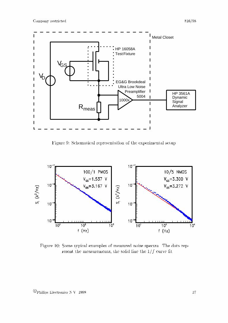
The experimental setup, used for the low-frequency noise measurements, is schemat-
ically depicted in Fig. 9. The device under study, which is packaged, is mounted in
a HP test �xture. The variable voltage sources VGS and VD consist of a battery and
a potentiometer. The current uctuations SI of the MOSFET are transformed into
voltage uctuations SV = SI �R2meas across the measurement resistor Rmeas = 1 k.
These voltage uctuations, in turn, are ampli�ed by an ultra-low noise ampli�er,
which is also fed by batteries. The entire setup, described so far, is shielded by
a metal closet in order to avoid unwanted interference signals (mainly 50 Hz and
higher harmonics), that may spoil the noise measurements. The ampli�ed noise
signal is now fed into a spectrum analyzer, located outside the metal closet. The
spectrum analyzer is controlled by a personal computer running a dedicated Lab-
View program. The noise spectrum was measured in the frequency range 1-1000 Hz.
Each spectrum was measured 8 times. This was done in order to check the valid-
ity of the measurements (no outliers). From these 8 spectra, both the average and
the standard deviation associated with each measurement frequency were calculated.
Typically, this standard deviation appeared to be � 10 % of the measurement value.
Using the experimental setup described above, noise spectra were measured for
both p-channel and n-channel devices of di�erent geometries. Most measurements
were performed in the saturation regime, where VDS was kept at � 3:3 V. For each
measurement, it was checked that it exceeds the background noise contributions of
low-noise-ampli�er and measurement resistor signi�cantly.
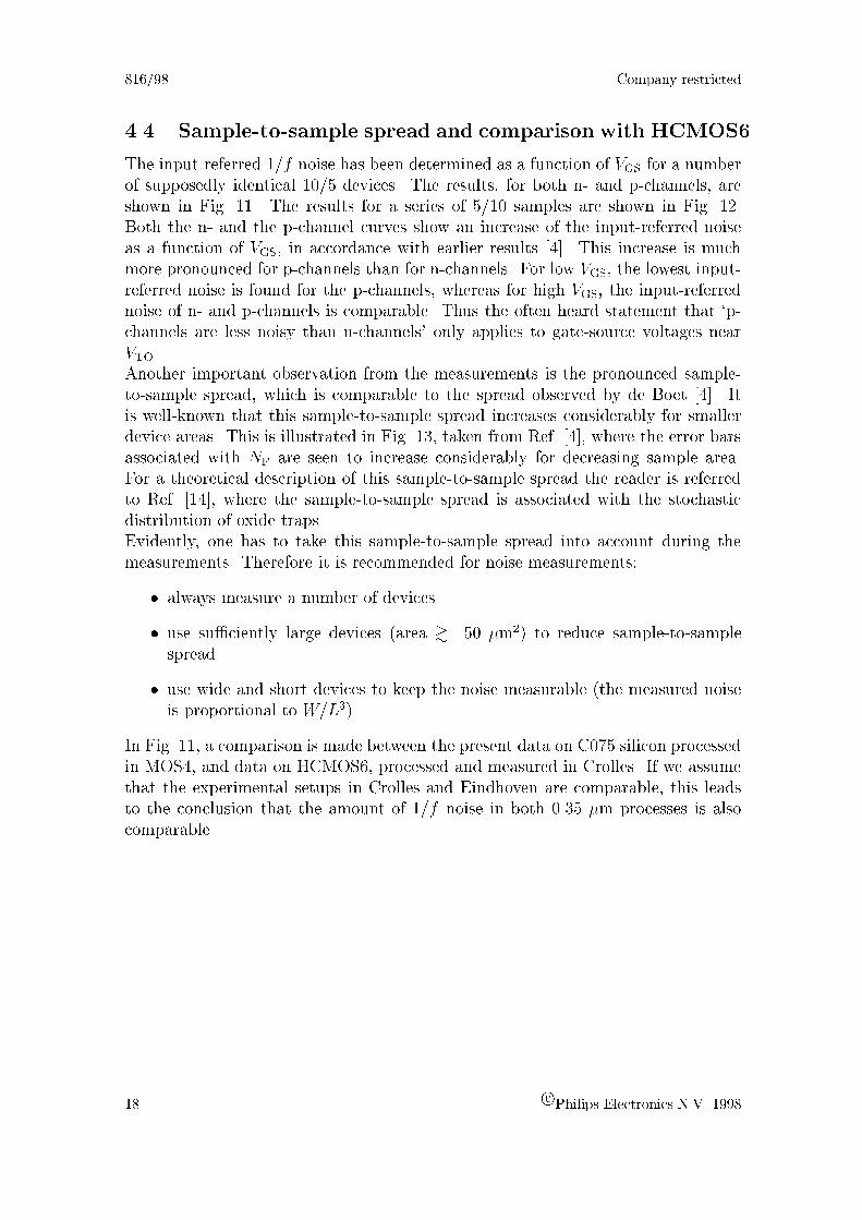
The spectra all showed a 1=f -like behavior. A 1=f spectral density was �tted to
the noise spectrum. Sometimes a white noise contribution was added to account for
background noise contributions. Some typical examples of measurements and curve
�ts are shown in Fig. 10. The standard deviations, determined as explained in the
previous section, were taken into account in the curve �tting.
The result of the 1=f curve �t is a voltage noise spectral density at 1 Hz, which
applies to the output of the low noise ampli�er. From this we calculate the voltage
noise at the input of the ampli�er by dividing by 10002, i.e. the square of the
ampli�er gain. Subsequently, the current noise spectral density of the MOSFET
is found by dividing by R2meas. Finally, as explained in Sec. 2.2, the input-referred
voltage noise is obtained by dividing by g2m. The value of gm was obtained from the
DC parameter set.
16c Philips Electronics N.V. 1998
Company restricted 816/98
V
.
GS
Rmeas
HP 16058A
VD
Test Fixture
EG&G BrookdealUltra Low Noise
Preamplifier HP 3561A DynamicSignalAnalyzer
50041000x
Metal Closet
Figure 9: Schematical representation of the experimental setup.
Figure 10: Some typical examples of measured noise spectra. The dots rep-
resent the measurements, the solid line the 1=f curve �t.
c Philips Electronics N.V. 1998 17
816/98 Company restricted
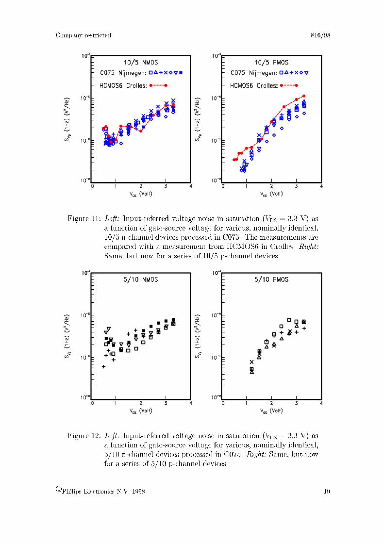
4.4 Sample-to-sample spread and comparison with HCMOS6
The input-referred 1=f noise has been determined as a function of VGS for a number
of supposedly identical 10/5 devices. The results, for both n- and p-channels, are
shown in Fig. 11. The results for a series of 5/10 samples are shown in Fig. 12.
Both the n- and the p-channel curves show an increase of the input-referred noise
as a function of VGS, in accordance with earlier results [4]. This increase is much
more pronounced for p-channels than for n-channels. For low VGS, the lowest input-
referred noise is found for the p-channels, whereas for high VGS, the input-referred
noise of n- and p-channels is comparable. Thus the often heard statement that `p-
channels are less noisy than n-channels' only applies to gate-source voltages near
VTO.
Another important observation from the measurements is the pronounced sample-
to-sample spread, which is comparable to the spread observed by de Boet [4]. It
is well-known that this sample-to-sample spread increases considerably for smaller
device areas. This is illustrated in Fig. 13, taken from Ref. [4], where the error bars
associated with NF are seen to increase considerably for decreasing sample area.
For a theoretical description of this sample-to-sample spread the reader is referred
to Ref. [14], where the sample-to-sample spread is associated with the stochastic
distribution of oxide traps.
Evidently, one has to take this sample-to-sample spread into account during the
measurements. Therefore it is recommended for noise measurements:
� always measure a number of devices.
� use su�ciently large devices (area & 50 �m2) to reduce sample-to-sample
spread.
� use wide and short devices to keep the noise measurable (the measured noise
is proportional to W=L3).
In Fig. 11, a comparison is made between the present data on C075 silicon processed
in MOS4, and data on HCMOS6, processed and measured in Crolles. If we assume
that the experimental setups in Crolles and Eindhoven are comparable, this leads
to the conclusion that the amount of 1=f noise in both 0.35 �m processes is also
comparable.
18c Philips Electronics N.V. 1998
Company restricted 816/98
Figure 11: Left: Input-referred voltage noise in saturation (VDS = 3:3 V) as
a function of gate-source voltage for various, nominally identical,
10/5 n-channel devices processed in C075. The measurements are
compared with a measurement from HCMOS6 in Crolles. Right:
Same, but now for a series of 10/5 p-channel devices.
Figure 12: Left: Input-referred voltage noise in saturation (VDS = 3:3 V) as
a function of gate-source voltage for various, nominally identical,
5/10 n-channel devices processed in C075. Right: Same, but now
for a series of 5/10 p-channel devices.
c Philips Electronics N.V. 1998 19

816/98 Company restricted
Figure 13: NF as a function of device area for the C100T5 process (Crolles).
The inrease of the error bars for smaller device areas is due to the
increasing sample-to-sample spread (from Ref. [4]).
4.5 Veri�cation of the geometrical scaling rules
Almost all noise models have a geometrical scaling
SVgate /1
WELE
(21)
The new level 903 1=f noise model is no exception to this. The major geometrical
scaling properties of this model are found in the scaling rules for the parameters
NFA, NFB, NFC:
NFA = NFAR �WERLER
WELE
NFB = NFBR �WERLER
WELE
NFC = NFCR �WERLER
WELE
(22)
Apart from this there are some implicit geometrical scaling via second-order e�ects
in IDS, scaling of the �-parameters, and the term that depends quadratically on IDS.
In order to verify this geometrical scaling, we performed noise measurements on a
series of 11 di�erent geometries (see Table 1) for both n- and p-channels. For all the
20c Philips Electronics N.V. 1998

Company restricted 816/98
geometries, the input-referred noise voltage was determined as a function of gate-
source voltage for VDS = 3:3 V. This value was multiplied by the e�ective device
area, and divided by the e�ective area of the reference device (the 10/0.35 device).
The 1=f noise of the 10/5 and 5/10 devices could be measured from somewhat
above threshold up to the supply voltage. Devices which are wider and shorter,
however, have a much larger gm, and therefore also a larger DC and 1=f noise
current. Therefore these devices could be measured also in the subthreshold regime.
However, they could not be measured for gate voltages as high as the supply voltage,
because the current drive capability of the experimental setup was not large enough
to keep the devices in saturation.
The results are shown in Fig. 14. It is observed that all measurements merge nicely
onto one curve. No systematic deviations for short-channel devices are observed,
and the deviations between di�erent geometries are of the same order of magnitude
as the sample-to-sample spread for one geometry (cf. Sec. 4.4). This leads to
the conclusion that the geometrical scaling rules of the new 1=f noise model are
su�ciently accurate.
W
E�
LE
W
ER�
LER
�
SVgate(V
2=Hz)
Figure 14: Left: Input-referred voltage noise in saturation (VDS = 3:3 V),
multiplied by the ratio of e�ective device area and e�ective refer-
ence device area, as a function of gate-source voltage, for a series
of n-channel geometries. Right: Same, but now for a series of
p-channel geometries.
c Philips Electronics N.V. 1998 21

816/98 Company restricted
4.6 Parameter extraction
We have used the following parameter extraction strategy:
� Only data were used with VDS > VGT (the saturation region is the most im-
portant region for circuit simulation). Included were the measurements of
Figs. 11, 12, and 14.
� All these data are used simultaneously in �tting NFAR, NFBR, NFCR.
� In compact modelling we rather overestimate the noise than underestimate it.
Therefore we forced the �tted curve to the upper side of the measurements.
This was achieved in the �tting program, by taking the error, assigned to a
situation where the calculated noise exceeds the measured noise, twice the
error of the opposite situation.
� For the n-channels, NFCR was not necessary, and set to zero.
The resulting curve �t is shown in Fig. 15 for the series of 11 geometries. For
comparison, the level 902 model with the parameters from the 1.03 (A3) process
block is shown as well. All the parameters are listed in table 3.
W
E�
LE
W
ER�
LER
�
SVgate(V
2=Hz)
W
E�
LE
W
ER�
LER
�
SVgate(V
2=Hz)
Figure 15: Same as Fig. 14, but now with the new 1=f noise model (solid
line), and the level 902 1=f noise model (dashed line).
N-channels P-channels
NFAR (V�1m�4) 39:8� 1023 15:4� 1023
NFMOD=1 NFBR (V�1m�2) 3:24� 108 0:179� 108
NFCR (V�1) 0 0:148� 10�7
NFMOD=0 NFR (V2) 19:91� 10�11 5:81� 10�11
Table 3: Recommended 1=f noise parameters for C075. The parameters
NFAR, NFBR, NFCR have been extracted from the present measure-
ments. The parameters NFR for the level 902 model are those found
in the 1.03 (or A3) process block.
22c Philips Electronics N.V. 1998

Company restricted 816/98
4.7 Improved modelling accuracy in the linear regime
The parameter extraction, as discussed above, is entirely based on saturation region
data, because of the importance of the saturation region in circuit design. It is still
interesting, however, to see how well the new model behaves in the linear regime. To
investigate this, the 10/5 p-channel device was measured for several gate voltages,
and for drain voltages ranging from 0.1 to 3.3 Volt. The result is shown in Fig. 16.
The solid lines are calculated using the new model and the parameters extracted in
the previous paragraph. The dashed line again represents the level 902 model.
Note that the calculated curves overestimate the noise somewhat throughout the
whole bias range. We will explain the reason for this now. The 10/5 p-channel
device was one of the devices discussed in the previous section. Thus the data
points for VDS = 3:3 V are also found in the right part of Fig. 15 (the triangles M).It is seen in that �gure that this particular device has a noise level which is somewhat
lower than `average' (i.e. the model curve). Therefore the model curves in Fig. 16,
which are based on the same parameters, overestimate the noise as well.
Evidently, the modelling accuracy in the linear regime is enhanced considerably,
even though linear region data have not been taken into account in the parameter
extraction. Doing so would of course enhance the modelling accuracy even more.
Figure 16: Input-referred 1=f noise for a 10/5 p-channel device for a number
of bias points in both linear and saturation regime. The solid
line represents the new model, evaluated using the parameters
extracted in Sec. 4.6. The dashed line corresponds to the MOS
Model 902 1=f noise model, using NFR from the 1.03 (or A3)
process block.
c Philips Electronics N.V. 1998 23

816/98 Company restricted
24c Philips Electronics N.V. 1998
Company restricted 816/98
5 Conclusion
MOS Model 9, level 903, contains a new 1=f noise model, which accounts for the VGSdependence of the input-referred noise, found in experiments. The model contains
three new parameters, NFAR, NFBR, and NFCR, and a switch NFMOD that selects
either the old (NFMOD=0) or the new (NFMOD=1) 1=f noise model. The physical
background of this model has been elucidated in this report.
Noise measurements have been performed on C075 silicon. This led to the following
conclusions:
� The present 1/f noise measurements on 0.35 �m silicon from Nijmegen are
comparable to the measurements performed in Crolles on HCMOS6. This is
an indication that both measurement setups are in order and that the amount
of 1/f noise in both processes is comparable.
� The geometrical scaling rules have been veri�ed experimentally, in particular
for very wide, short devices that are important in real circuits.
� The new 1/f noise model gives much better results than the level 902 1/f noise
model, in all operating regimes of the MOSFET.
� The following set of parameters is recommended for C075:
N-channels P-channels
NFAR (V�1m�4) 39:8� 1023 15:4� 1023
NFMOD=1 NFBR (V�1m�2) 3:24� 108 0:179� 108
NFCR (V�1) 0 0:148� 10�7
NFMOD=0 NFR (V2) 19:91� 10�11 5:81� 10�11
Acknowledgments
I would like to thank Peter de Vreede for designing the C075 1=f noise test struc-
tures, and Heinze Elzinga for putting them on the multiproject wafer. Adrie Zegers
is acknowledged for her help in the noise measurements.
c Philips Electronics N.V. 1998 25

816/98 Company restricted
26c Philips Electronics N.V. 1998

Company restricted 816/98
A Noise in MOSFETs: theory
A.1 General method for noise calculations in MOSFETs
First we will address the question how to calculate the current noise SI(f) on the
output terminals of a MOSFET if we know the current noise sources h(x; t) inside
the device. We follow Refs. [7, 8, 15]. Note that the derivation is in terms of the
quasi-Fermi potential V , which makes the results valid when we have either drift,
di�usion or both as transport mechanism. In other words, the result applies to the
weak, moderate, and strong inversion regimes of the MOSFET.
The current IDS is given by:
IDS = g(x)dV
dx(23)
where V is de quasi-Fermi potential of the electrons g(x) is given by
g(x) = �W�e�Qi(x) (24)
where Qi(x) is the inversion charge density in C/m2.
If we have a current noise source h(x; t) in the channel the current will be IDS +
�IDS(t) and the quasi-Fermi potential will be V + �V (t). We assume that the
source and drain voltages are constant (only IDS uctuates), so that �V (t) = 0 for
x = 0 and x = L. We have
IDS +�IDS(t) = g(V +�V (t))d(V +�V (t))
dx+ h(x; t) (25)
For small uctuations this can be written using Taylor expansion as:
IDS +�IDS(t) �
�g(V ) +
dg
dV�V (t)
��dV
dx+d�V (t)
dx
�+ h(x; t)
� g(V )dV
dx+ g(V )
d�V (t)
dx+
dg
dV
dV
dx�V (t) + h(x; t)
= g(V )dV
dx+
d
dx[g(V )�V (t)] + h(x; t) (26)
The �rst term on the right side is equal to IDS, so that the above equation reduces
to:
�IDS(t) =d
dx[g(V )�V (t)] + h(x; t) (27)
Now we integrate both sides of the equations from x = 0 to x = L. The �rst term
on the right side now vanishes because of the boundary conditions �V (t) = 0 for
x = 0 and x = L. Now we �nd:
�IDS(t) =1
L
Z L
0
h(x; t)dx (28)
Now we have the relation between the current noise sources h(x; t) inside the device
and the current uctuations �IDS(t) observed in the leads. In order to express this
c Philips Electronics N.V. 1998 27
816/98 Company restricted
relation in terms of noise spectral densities, we �rst calculate the autocorrelation
function of �IDS(t), i.e. the average (over time t) �IDS(t)�IDS(t+ s),
�IDS(t)�IDS(t+ s) =1
L
Z L
0
h(x; t)dx1
L
Z L
0
h(x0; t+ s)dx0
=1
L2
Z L
0
Z L
0
h(x; t)h(x0; t+ s)dxdx0 (29)
TheWiener-Khintchine theorem states that the noise spectral density of a quantity is
equal to twice the Fourier transform of the autocorrelation function [7, 8]. Applying
this theorem to both sides of Eq. (29), the noise spectral density, SI(f), is found:
SI(f) =1
L2
Z L
0
Z L
0
Sh(x; x0
; f)dxdx0 (30)
where Sh(x; x0; f) is the `spatial cross-spectral intensity' of the noise. Now we as-
sume that we have spatially uncorrelated current noise sources. This means that
Sh(x; x0; f) can be written as the product of a Dirac �-function �(x0 � x) and a
function F that only depends on x0 and f :
Sh(x; x0
; f) = F(x0; f)�(x0 � x) (31)
Thus for uncorrelated current noise sources we �nd:
SI(f) =1
L2
Z L
0
F(x; f)dx (32)
If we evaluate SI(f) in a section between x and (x + �x) (we call this quantity
SI;�x(x; f)), we �nd:
SI;�x(x; f) =1
�x2
Z �x
0
F(x; f)dx =F(x; f)
�x(33)
Now we know the meaning of F(x; f):
F(x; f) = SI;�x(x; f) ��x (34)
Using this result in Eq. (32) we �nally obtain:
SI(f) =1
L2
Z L
0
S�I(x; f) ��x � dx (35)
Note again that this equation applies to the general case that we have both drift and
di�usion. Thus it is equally valid in the subthreshold and strong inversion regimes.
The formula (35) is somewhat counterintuitive. In fact, most people starting with
noise calculations in MOSFETs would guess:
SV (f) =
Z L
0
SV;�x(x; f)
�xdx (36)
where SV;�x(x; f) is the voltage noise spectral density of a segment �x. This method
of calculating the noise is sometimes referred to as the \Salami method". Generally,
it gives wrong results because it assumes the voltage noise spectral densities of two
device segments to be uncorrelated. A discussion of this subject is found in Ref.[16].
28c Philips Electronics N.V. 1998

Company restricted 816/98
A.2 Application of Hooge's law to a MOSFET
1=f noise is often characterized using \Hooge's law", which is an empirical relation
that reads as follows:
SI = �H �I2
N�1
f(37)
where �H is the Hooge constant and N is the total number of charge carriers.
We will now evaluate Hooge's law for a MOSFET, following Ref. [17]. Consider a
segment �x of the channel, containing �N charge carriers. Applying Hooge's law
to this channel segment gives:
S�I(x; f) = �H �I2DS
�N�1
f(38)
The integration from source to drain is performed according to Eq. 35. Thus we
assume that the current noise sources associated with each channel segment are
uncorrelated. Now we arrive at:
SI =�HIDS
fL2�
Z L
0
IDS�xdx
�N(39)
Now we use that �N = �WQi(x)�x=q, and IDS = �W�e�Qi(x)dVdx
[i.e. Eqs. (23)
and (24)]:
SI =�HqIDS�e�
fL2�
Z L
0
dV
dxdx (40)
This �nally leads to:
SI = �H �q�e�IDSVDS
fL2(41)
The above formula should be valid both in subthreshold and strong inversion.
A simple formula for the strong inversion regime is obtained if we use the basic drain
current expression
IDS = �e�Cox
W
L(VGT �
1
2VDS) � VDS (42)
Now we �nd for the input referred voltage noise in strong inversion:
SVgate =�Hq(VGT �
12VDS)
WLCoxf(43)
This result is sometimes referred to as the `Kleinpenning model'. Usually it is
assumed that the contribution of the pinch-o� region is negligible, as con�rmed by
the experiments (see Fig. 16). Then, in saturation we can simply replace VDS in the
above formula by VDSAT � VGT, so that:
SVgate =�HqVGT
2WLCoxf(44)
c Philips Electronics N.V. 1998 29

816/98 Company restricted
30c Philips Electronics N.V. 1998

Company restricted 816/98
B The level 903 1=f noise model
B.1 Derivation of the model by Hung et al.
In this section, we will elucidate the mathematical derivation of the new 1=f noise
model. This is not meant to be exhaustive, but meant to give the reader an idea
how the seemingly di�cult formulae of this model come about. For a full derivation
we refer to the original papers [9, 10].
The derivation starts with a calculation of the uctuations in the number of occu-
pied traps at a position x in the channel (x is the direction from source to drain).
According to conventional number uctuation theory this is given by:
S�Nt(x; f) =Z Ec
Ev
Z W
0
Z tox
0
4nt(E; x; y; z)�x fFD(1� fFD)�
1 + 4�2f 2� 2dz dy dE (45)
Integration has to be performed over the di�erent trap depths z, over the various trap
energies E, and �nally over the channel widthW (i.e. the y direction). It is assumed
that the distribution of traps is spatially uniform (i.e. nt(E; x; y; z) = nt(E)). The
factor fFD(1 � fFD) expresses that a trapping process can only take place from a
�lled state to a non-�lled state or vice versa (fFD = [1+exp(E�Efn))=kBT ]�1 is the
Fermi-Dirac trap occupancy function). Because fFD(1 � fFD) behaves like a delta
function around the quasi-Fermi level, nt(E) can be replaced by nt(Efn) and taken
out of the integral. The time constant � is given by:
� = �0(E) � exp( oxz) (46)
where �0(E) is the time constant at the interface and ox is the attenuation co-
e�cient of the electron wave function in the gate oxide. For tox � 1= ox and
f � 1=(2��0(E)), the integration over z and y yields:
S�Nt(x; f) =nt(Efn)�xW
oxf�
Z Ec
Ev
fFD(1� fFD) dE (47)
Now the integration over the energy E has to be performed. This is facilitated using
the equality
fFD(1� fFD) = �kBT �dfFD
dE(48)
Using fFD(Ec) � 0 and fFD(Ev) � 1 one arrives at:
S�Nt(x; f) � nt(Efn)kBT W�x
ox f(49)
Now that we know the uctuations in the number of occupied traps at position x in
the channel, we are interested in their e�ect on the drain current IDS. As explained
c Philips Electronics N.V. 1998 31
816/98 Company restricted
in the Sec. 3, the uctuations of mobility and carrier number are correlated. This
leads to [10]:
SI;�x(x; f) = S�Nt(x; f)
�IDS
NW�x(R� �S�e�N)
�2(50)
Here, N is the carrier density, �e� is the e�ective mobility, and �S is a scattering
coe�cient, responsible for the mobility uctuations. It has been found from inde-
pendent measurements that �S is typically 10�15 Vs, and that its value decreases
with increasing carrier density due to screening e�ects. Furthermore, the ratio R is
introduced, de�ned as:
R �@�N
@�Nt
(51)
This ratio R can be expressed as:
R = �Ci
Cox + Ci + Cd + Cit
(52)
where Cox, Ci, Cd and Cit are the oxide, inversion layer, depletion layer, and interface
trap capacitances, respectively. Using Ci �q2
kBTN , this can be rewritten as
R = �N
N +N�
(53)
with
N� =
kBT
q2(Cox + Cd + Cit) (54)
Note that R approaches �1 in strong inversion.
Now we are ready to perform the integration over the channel length. Assuming
that the current noise sources in each part �x of the channel are uncorrelated, the
correct method to calculate the total noise in the drain current is:
SI(f) =1
L2
Z L
0
SI;�x(x; f)�x dx (55)
This formula is not trivial. The derivation, after van der Ziel, is shown in appendix A.
Combining Eqs. (50) and (55) leads to:
SI(f) =kBTI
2DS
oxfWL2
Z L
0
nt(Efn)
�R
N(x)� �S�e�
�2dx (56)
Just as in the derivation of IV models, it is convenient to replace the integration
over x by integration over the quasi-Fermi potential V , using Eqs. (23) and (24),
which leads to
SI(f) =kB T q IDS �e�
ox f L2
Z VDS
0
nt(Efn)R2
N(1� �S�e�
N
R)2 dV (57)
32c Philips Electronics N.V. 1998

Company restricted 816/98
To proceed further, one needs to know the bias dependence of �S, �e� , and nt(Efn).
In order to keep things mathematically feasible, the following parametrization is
made:
nt(Efn)(1� �S�e�N
R)2 = A +BN + CN
2 (58)
Using qN(x) = Cox � [VGT � aV (x)] one can replace the integration over V by
integration overN . Here a is the factor that corrects for the variation of the depletion
region depth going from source to drain, i.e. (1+ �1) in MOS Model 9. In the linear
regime, we arrive at:
SI(f) =kBTq
2IDS�e�
a oxfL2Cox
�A ln
N0 +N�
NL +N�
+B(N0 �NL) +1
2C(N2
0 �N2L)
�(59)
where N0 and NL are the charges at the source and drain end of the channel,
respectively:
N0 =Cox
q� VGT (60)
and
NL =Cox
q� (VGT � aVDS) (61)
In saturation, there is an additional contribution of the pinch-o� region. We will
not show the derivation here. According to Refs. [9, 10] the expression for the drain
current icker noise now reads:
SI(f) =kBTq
2IDS�e�
a oxfL2Cox
�A ln
N0 +N�
NL +N�
+B(N0 �NL) +1
2C(N2
0 �N2L)
�
+�L �kBTI
2DS
oxfWL2�A +BNL + CN
2L
(NL +N�)2(62)
In the subthreshold region, the noise turns out to be:
SI(f) =AkBTI
2DS
WL oxfN�2
(63)
Here, terms with B and C are neglected.
B.2 Rewriting Hung's model in MOS Model 9 terms
Now we will show how we have rewritten the model by Hung et al. in MOS Model 9
terms. First, the factor a = 1 + �1 is dropped from Eqs. (61) and (62). We have
made this approximation to keep our model compatible with the BSIM3v3 imple-
mentation [11], which makes the same approximation. This has, however, quite
some e�ect on the magnitude of the calculated noise, as shown in Fig. 17.
c Philips Electronics N.V. 1998 33
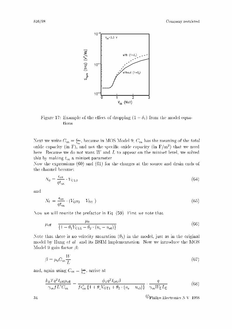
816/98 Company restricted
Figure 17: Example of the e�ect of dropping (1 + �1) from the model equa-
tions.
Next we write Cox =�oxtox, because in MOS Model 9, Cox has the meaning of the total
oxide capacity (in F), and not the speci�c oxide capacity (in F/m2) that we need
here. Because we do not want W and L to appear on the miniset level, we solved
this by making tox a miniset parameter.
Now the expressions (60) and (61) for the charges at the source and drain ends of
the channel become:
N0 =�ox
qtox� VGT3 (64)
and
NL =�ox
qtox� (VGT3 � VDS1) (65)
Now we will rewrite the prefactor in Eq. (59). First we note that
�e� =�0
f1 + �1VGT1 + �2 � (us � us0)g(66)
Note that there is no velocity saturation (�3) in the model, just as in the original
model by Hung et al. and its BSIM implementation. Now we introduce the MOS
Model 9 gain factor �:
� = �0Cox
W
L(67)
and, again using Cox =�oxtox, arrive at
kBTq2IDS�e�
oxfL2Cox
=�Tq
2IDS�
f�2ox f1 + �1VGT1 + �2 � (us � us0)g�
q
oxWELE
(68)
34c Philips Electronics N.V. 1998
Company restricted 816/98
Note that we replaced the drawn channel dimensions W and L by the electrical
dimensionsWE and LE. Now we introduce the MOS Model 9 noise parameters NFA,
NFB, and NFC:
NFA = A �q
oxLEWE
NFB = B �q
oxLEWE
(69)
NFC = C �q
oxLEWE
Therefore in strong inversion, the 1/f noise spectral density, denoted by Ssi, expressed
in MM9 terms, reads:
Ssi =�T q
2IDS � t
2ox
f�2ox f1 + �1VGT1 + �2 � (us � us0)g�
�NFA � ln
N0 +N�
NL +N�
+NFB � (N0 �NL) +1
2�NFC � (N
20 �N
2L)
�(70)
Now we need to rewrite the pinch-o� term. Therefore we need an expression for
the channel-length-modulation �L in MOS Model 9 terms. In case of pinch-o�, the
drain current is proportional to:
WE
LE ��L=
WE
LE
�1
1� �LLE
�WE
LE
�G2 (71)
where G2 = 1=(1 + (�L=LE)) is the MOS Model 9 factor describing channel length
modulation (see Eq. (2.25) in Ref. [2]). Now we see that we may write:
�L
LE
=G2 � 1
G2
(72)
Note that we have �L = 0 when G2 = 1, as expected. Now the full expression for
the noise in the saturation region is readily found to be:
Ssi =�T q
2IDS � t
2ox
f�2ox f1 + �1VGT1 + �2 � (us � us0)g�
�NFA � ln
N0 +N�
NL +N�
+NFB � (N0 �NL) +1
2�NFC � (N
20 �N
2L)
�
+�T I
2DS
f�G2 � 1
G2
�
�NFA +NFBNL +NFCN
2L
(NL +N�)2
�(73)
Similarly, we rewrite the 1/f noise spectral density in weak inversion, denoted by
Swi:
Swi =AkBTI
2DS
WL oxfN�2
= NFA ��TI
2DS
fN�2(74)
c Philips Electronics N.V. 1998 35

816/98 Company restricted
B.3 The transition between weak and strong inversion
So far, we have shown separate expressions for Swi and Ssi, the icker noise in the
weak and strong inversion regimes. In the BSIM3v3 model the icker noise S in
the drain current is calculated as follows:
if VGT > 0:1 V then : S = Ssi
else : S =Ssi(VGT = 0:1 V)� Swi
Ssi(VGT = 0:1 V) + Swi(75)
This transition is not very smooth, as depicted in the left frame of Fig. 18. Therefore
we improved this transition for the MOS Model 9 implementation of the model:
S =Ssi � Swi
Ssi + Swi(76)
As shown in the right frame of Fig. 18, this transition has indeed been smoothed.
Moreover, our expression for S approaches the Swi line much better in the weak
inversion regime.
Note that this transition has the consequence that the parameter NFA has to be
non-zero. This is because if NFA = 0, the noise in weak inversion Swi becomes zero
as well, see Eq. (74). The �nal result S , in turn, see Eq. (76), will also vanish.
Figure 18: The transition from weak to strong inversion in the BSIM3v3
model (left) and in MOS Model 903 (right).
36c Philips Electronics N.V. 1998
Company restricted 816/98
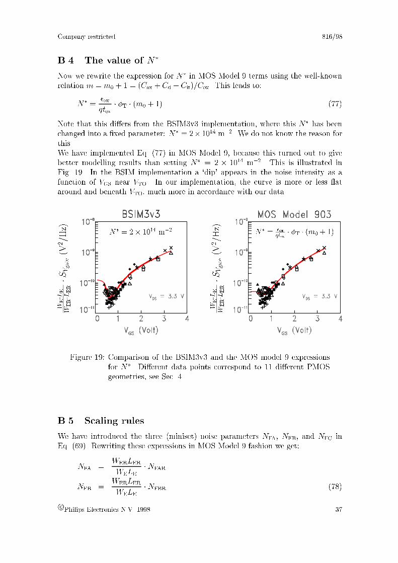
B.4 The value of N�
Now we rewrite the expression for N� in MOS Model 9 terms using the well-known
relation m = m0 + 1 = (Cox + Cd + Cit)=Cox. This leads to:
N� =
�ox
qtox� �T � (m0 + 1) (77)
Note that this di�ers from the BSIM3v3 implementation, where this N� has been
changed into a �xed parameter: N� = 2� 1014 m�2. We do not know the reason for
this.
We have implemented Eq. (77) in MOS Model 9, because this turned out to give
better modelling results than setting N� = 2 � 1014 m�2. This is illustrated in
Fig. 19. In the BSIM implementation a `dip' appears in the noise intensity as a
function of VGS near VTO. In our implementation, the curve is more or less at
around and beneath VTO, much more in accordance with our data.
N�
= 2� 1014m�2
W
E�
LE
W
ER�
LER
�
SVgate(V
2=Hz)
N� = �ox
qtox� �T � (m0 + 1)
W
E�
LE
W
ER�
LER
�
SVgate(V
2=Hz)
Figure 19: Comparison of the BSIM3v3 and the MOS model 9 expressions
for N�. Di�erent data points correspond to 11 di�erent PMOS
geometries, see Sec. 4.
B.5 Scaling rules
We have introduced the three (miniset) noise parameters NFA, NFB, and NFC in
Eq. (69). Rewriting these expressions in MOS Model 9 fashion we get:
NFA =WERLER
WELE
�NFAR
NFB =WERLER
WELE
�NFBR (78)
c Philips Electronics N.V. 1998 37

816/98 Company restricted
NFC =WERLER
WELE
�NFCR
where we have introduced the maxiset noise parameters NFAR, NFBR, and NFCR.
Note that the geometrical scaling rules of the model parameters are identical to
that of NFR in MOS MODEL 9, level 902. In fact, most 1=f noise models, have the
same geometrical scaling:
SVgate /1
WELE
(approximately) (79)
The three new noise parameters on the maxiset level are NFAR, NFBR, NFCR. These
are related to the A, B, and C introduced in Eq. (58) by:
NFAR = A �q
oxLERWER
(80)
NFBR = B �q
oxLERWER
(81)
NFCR = C �q
oxLERWER
(82)
Finally we note that there are no explicit temperature scaling rules of the parameters.
However, the model equations have an implicit temperature dependence via �T
(� kBT=q).
B.6 Simpli�ed model and physical interpretation of the pa-
rameters
If we simplify the model, following Ref. [18], a physical interpretation of the new
noise parameters can be given. This simpli�cation neglects the dependences of
nt(Efn), �S, and �e� on carrier density N . Doing so, combination of Eqs. (58), (80),
(81), (82) gives us the following physical interpretation of the noise parameters:
NFAR = nt �q
oxLERWER
(83)
NFBR = 2�S�e�NFAR (84)
NFCR =N
2FBR
4NFAR
(85)
Thus from the parameter NFAR an \average" trap density nt can be calculated. For
NMOS, one typically �ndsNFAR � 1024V�1m�4 corresponding to nt = 2� 1041m�3J�1.
Next, an \average" scattering coe�cient �S can be derived from NFBR. For a typical
value NFBR � 108V�1m�2 and �e� = 0:04m2=Vs we arrive at �S = 10�15 Vs. Note
that in this simpli�ed model NFCR is not a free parameter anymore but follows
directly from NFAR, NFBR. Thus if one is really interested in deriving values for ntand �S from 1=f noise measurements, it makes sense to extract the noise parameters
under the constraint (85), as proposed in Ref. [18].
Note that in MOS Model 9, we do not use this simpli�ed model, and we do not
recommend it for the purpose of compact modelling for circuit simulation.
38c Philips Electronics N.V. 1998

Company restricted 816/98
B.7 Hooge's law
The situation where the term with NFB is the dominant term is of special interest.
This is the case when mobility scattering is the dominant mechanism, and NFC is
not too big. In such a case, Eq. (59) in strong inversion simpli�es to:
Ssi = (NFBR � LER �WER � �T) �q�e�IDSVDS
fL2(86)
This is exactly the same equation that we found in Appendix A by applying Hooge's
law to a MOSFET, see Eq. (43), if we take the Hooge constant �H to be equal to:
�H = NFBR � LER �WER � �T (87)
Applying this to the values of NFBR found in our parameter extraction, we �nd for
�H values of � 10�5 for NMOS and � 10�6 for PMOS devices.
c Philips Electronics N.V. 1998 39
816/98 Company restricted
40c Philips Electronics N.V. 1998

Company restricted 816/98
C List of used symbols
Here we list the symbols used in this report, �rst the Greek symbols and then the
Roman symbols.
symbol description unit
�H Hooge constant {
�S scattering coe�cient Vs
� MOS Model 9 gain factor (miniset parameter) A/V2
frequency exponent of icker noise {
ox attenuation coe�cient of electron wave function in gate oxide m�1
�(x0 � x) Dirac delta-function m�1
�1 accounts for depletion layer depth variation from source to drain {
�L length of pinch-o� region in saturation m
�ox absolute permittivity of gate oxide F/m
�1 MOS Model 9 mobility reduction parameter (gate �eld) V�1
�2 MOS Model 9 mobility reduction parameter (bulk �eld) V�12
�3 MOS Model 9 mobility reduction parameter (velocity saturation) V�1
�e� e�ective mobility, de�ned by Eq. (66) m2V�1s�1
�0 zero-�eld mobility m2V�1s�1
� time constant of a trap s
�0 time constant of a trap at the Si/SiO2 interface s
�B surface potential in strong inversion V
�T thermal voltage � kBT=q V
a used in Refs. [9, 10], corresponds to (1 + �1) in MOS Model 9 {
Cd depletion layer capacitance per area F/m2
Ci inversion layer capacitance per area F/m2
Cit interface traps capacitance per area F/m2
Cox speci�c oxide capacitance F/m2
E energy level J
Efn quasi-Fermi level of electrons J
f frequency Hz
fFD Fermi-Dirac occupancy function {
F noise �gure {
F(x; f) see Eq. (34) A2m/Hz
G carrier generation rate s�1
gm transconductance A/V
g(x) local conductivity, see Eqs. (23) and (24). m
G2 MOS Model 9 factor describing channel length modulation {
h(x; t) uctuating current inside the device A
i1=f icker noise current A
I current A
IDS current owing from source to drain A
kB Boltzmann constant JK�1
c Philips Electronics N.V. 1998 41
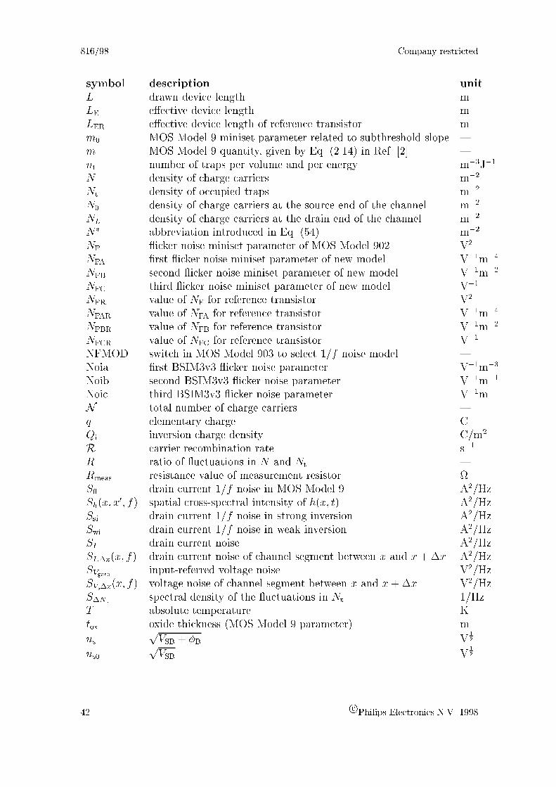
816/98 Company restricted
symbol description unit
L drawn device length m
LE e�ective device length m
LER e�ective device length of reference transistor m
m0 MOS Model 9 miniset parameter related to subthreshold slope {
m MOS Model 9 quantity, given by Eq. (2.14) in Ref. [2] {
nt number of traps per volume and per energy m�3J�1
N density of charge carriers m�2
Nt density of occupied traps m�2
N0 density of charge carriers at the source end of the channel m�2
NL density of charge carriers at the drain end of the channel m�2
N� abbreviation introduced in Eq. (54) m�2
NF icker noise miniset parameter of MOS Model 902 V2
NFA �rst icker noise miniset parameter of new model V�1m�4
NFB second icker noise miniset parameter of new model V�1m�2
NFC third icker noise miniset parameter of new model V�1
NFR value of NF for reference transistor V2
NFAR value of NFA for reference transistor V�1m�4
NFBR value of NFB for reference transistor V�1m�2
NFCR value of NFC for reference transistor V�1
NFMOD switch in MOS Model 903 to select 1=f noise model {
Noia �rst BSIM3v3 icker noise parameter V�1m�3
Noib second BSIM3v3 icker noise parameter V�1m�1
Noic third BSIM3v3 icker noise parameter V�1m
N total number of charge carriers {
q elementary charge C
Qi inversion charge density C/m2
R carrier recombination rate s�1
R ratio of uctuations in N and Nt {
Rmeas resistance value of measurement resistor
S drain current 1=f noise in MOS Model 9 A2/Hz
Sh(x; x0; f) spatial cross-spectral intensity of h(x; t) A2/Hz
Ssi drain current 1=f noise in strong inversion A2/Hz
Swi drain current 1=f noise in weak inversion A2/Hz
SI drain current noise A2/Hz
SI;�x(x; f) drain current noise of channel segment between x and x +�x A2/Hz
SVgate input-referred voltage noise V2/Hz
SV;�x(x; f) voltage noise of channel segment between x and x+�x V2/Hz
S�Nt spectral density of the uctuations in Nt 1/Hz
T absolute temperature K
tox oxide thickness (MOS Model 9 parameter) m
us
pVSB + �B V
12
us0
pVSB V
12
42c Philips Electronics N.V. 1998
Company restricted 816/98
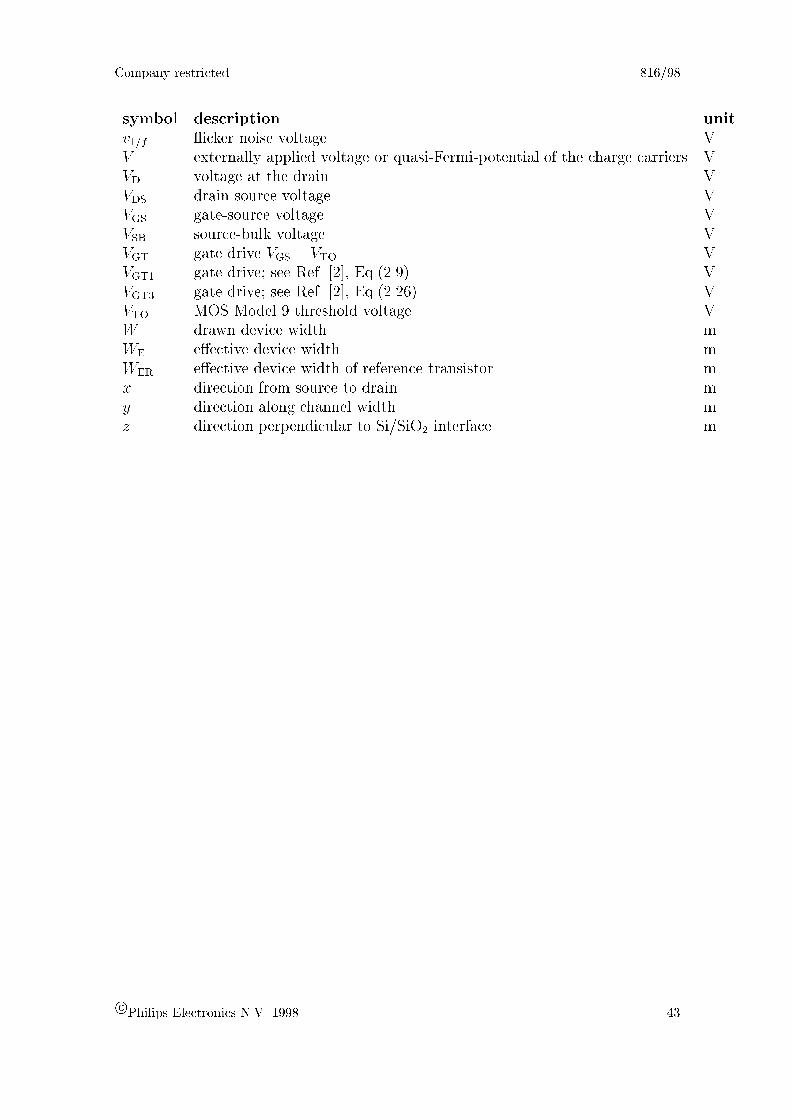
symbol description unit
v1=f icker noise voltage V
V externally applied voltage or quasi-Fermi-potential of the charge carriers V
VD voltage at the drain V
VDS drain-source voltage V
VGS gate-source voltage V
VSB source-bulk voltage V
VGT gate drive VGS � VTO V
VGT1 gate drive; see Ref. [2], Eq.(2.9) V
VGT3 gate drive; see Ref. [2], Eq.(2.26) V
VTO MOS Model 9 threshold voltage V
W drawn device width m
WE e�ective device width m
WER e�ective device width of reference transistor m
x direction from source to drain m
y direction along channel width m
z direction perpendicular to Si/SiO2 interface m
c Philips Electronics N.V. 1998 43

816/98 Company restricted
44c Philips Electronics N.V. 1998

Company restricted 816/98
References
[1] MOS Model Book, Dec. 1996, Philips ED & T/Analogue Simulation.
[2] R.M.D.A. Velghe, D.B.M. Klaassen, F.M. Klaassen, MOS Model 9 , Nat. Lab.
Unclassi�ed Report NL-UR 003/94.
[3] Internet: http://www.semiconductors.philips.com/Philips Models.
[4] J.A.M. de Boet and R.R.J. Vanoppen, 1/f noise characterization of C200 MOS
transistors, NL-TN 220/93;
1/f noise in buried/ surface channel PMOSFETs, 30-6-1994;
1/f noise characterization C100T5, unclassi�ed RWR-JB-950222-jb, 22-2-1995;
1/f noise characterization Qubic Nmos, 25-6-1993;
Verkennende LF-ruis metingen aan C150LP Pmos transistoren, 5-1-1993.
[5] A.J. Scholten and D.B.M. Klaassen, The thermal noise model in MOS Model 9,
in preparation.
[6] R. Vanoppen, RF noise characterization, NL-TN 134/97.
[7] A. van der Ziel, Noise: sources, characterization, measurement, Prentice-Hall,
1970.
[8] A. van der Ziel, Noise in measurements, John Wiley & Sons, 1976.
[9] Kwok K. Hung et al., A uni�ed model for the icker noise in metal-oxide-
semiconductor �eld-e�ect transistors, IEEE Trans El. Dev. Vol. 37, No. 3, March
1990.
[10] Kwok K. Hung et al., A physics-based MOSFET noise model for circuit simu-
lators, IEEE Trans El. Dev. Vol. 37, No. 5, May 1990.
[11] Yuhua Cheng et al., BSIM3v3 Manual, 1996, available from
http://rely.eecs.berkeley.edu:8080/bsim3www.
[12] A.J. Scholten and D.B.M. Klaassen, Modelling of 1=f noise in MOSFETs,
BMMWP#11, November 26th, Philips Nat.Lab. Eindhoven.
[13] A.J. Scholten and D.B.M. Klaassen, Modeling of 1=f noise for C075,
BMMWP#12, May 13th, Philips Nat.Lab. Eindhoven.
[14] G. Ghibaudo and O. Roux-dit-Buisson, Low-frequency uctuations in scaled
down silicon CMOS devices status and trends, Proc. ESSDERC '94, pp.693-700
(1994).
[15] F.M. Klaassen and J. Prins, Thermal noise of MOS transistors, Phil. Res.
Repts. 22, 504-514, 1967.
c Philips Electronics N.V. 1998 45

816/98 Company restricted
[16] K.M. van Vliet et al., Noise in single injection diodes. I. A Survey of methods,
Journal of Applied Physics, Vol. 46, No.4, April 1975, pp. 1804-1813.
[17] F.M. Klaassen, Characterization of low 1=f noise in MOS transistors, IEEE
Trans. El. Dev., Vol. ED-18, no.10, october 1971.
[18] M. van Heijningen, E. Vandamme, L. Deferm, and L.Vandamme, Modeling
1/f noise and extraction of the SPICE noise parameters using a new extraction
procedure, Proc. ESSDERC Conference '98.
46c Philips Electronics N.V. 1998

Company restricted 816/98
Author(s) A.J. Scholten and D.B.M. Klaassen
Title New 1/f noise model in
MOS Model 9, level 903
Distribution
Nat.Lab./PI WB-5
PRL Redhill, UK
PRB Briarcli� Manor, USA
LEP Limeil{Br�evannes, France
PFL Aachen, BRD
CP&T WAH
Adjunct-directeur: Ir. M.G. Collet WAG-14
Groepsleider: Dr. R. Woltjer WAG-14
Abstract
S. McIntosh COO o�ce BAE-2
A. van Gorkum CTO o�ce BAE-2
T. Claasen CTO o�ce BAE-2
J. Lohstroh CTO o�ce BAE-2
T. Akkermans Chief Strategy O�cer BAE-2
G. Groenendaal SPM telecom BAE-2
J. Verhoeks SPMM C-IC BAE-2
J.B. Theeten SPMM C-IC BAE-2
E. Odijk SPMM C+M BAE-2
R. v.d. Bij SPMM Discrete BAE-4
J. Bloos SPMM Discrete BAE-4
R. Sykes SPMM ASL Sunnyvale
A. Reader 46 Impasse des Buis, 38920 Crolles, France
P. Coppelmans S&V IC Lab. SFJ-6
R. Kluitmans CE.IC Lab SFJ-658
R. Braam CE.IC Lab SFJ-6
W. Leising CIC Hamburg LA 351
J. Meeuwis PCALE CAD Support Group BE-505
H. van Glabbeek PCAL-E BE-4
H. Otten SLE BE-5
H. Okel Philips RHW Hamburg
J. Fock Philips RHW Hamburg
G. Sieboerger Philips RHW Hamburg
J. Lebailly Philips Composants Caen
J. Journeau Philips Composants Caen
c Philips Electronics N.V. 1998 47
816/98 Company restricted
C. Biard Philips Composants Caen
E. Weagel Philips Semiconductors Albuquerque
N. Ho�man Philips Semiconductors BAE-2
L. Gambus Philips Semiconductors Caen
M. Bolt Philips Semiconductors Crolles
H. Grabe Philips Semiconductors Hamburg
T. Evelbauer Philips Semiconductors Hamburg
R. Grover Philips Semiconductors Hazel Grove
L. Gee Philips Semiconductors Southampton
B. Redman-White Philips Semiconductors Southampton
F. van Roosmalen Philips Semiconductors Stadskanaal
M. Shields Philips Semiconductors Sunnyvale
G. Conner Philips Semiconductors Sunnyvale
K. Davis Philips Semiconductors Sunnyvale
J. Hendrickx Philips Semiconductors WAY41
M. Locher Philips Semiconductors Z�urich
J. Solo Philips Semiconductors Z�urich
R. Penning de Vries Philips Semiconductors Nijmegen
W. Josquin Philips Semiconductors Nijmegen
A. Linssen Philips Semiconductors Nijmegen
M. Hillen Philips Semiconductors Nijmegen
H. Boezen Philips Semiconductors Nijmegen
J. Schmitz Philips Semiconductors Nijmegen
J. van der Pol Philips Semiconductors Nijmegen
G. de Groot Philips Semiconductors Nijmegen
Th. Smit Philips Semiconductors Nijmegen
H. van der Vlist Philips Semiconductors Nijmegen
M. Versleijen Philips Semiconductors Nijmegen
L. van de Hoven Philips Semiconductors Nijmegen
J. Bruines Philips Semiconductors Nijmegen
M. Berkhout Philips Semiconductors Nijmegen
M. van Dort Philips Semiconductors Nijmegen
J. Egbers Philips Semiconductors Nijmegen
P. Emonts Philips Semiconductors Nijmegen
L. Harm Philips Semiconductors Nijmegen
S. Nath Philips Semiconductors Nijmegen
R. Tuijtelaars Philips Semiconductors Nijmegen
J. Willms Philips Semiconductors Nijmegen
S. Onneweer ED&T Analogue Simulation WAY-31
H. Hermans ED&T Analogue Simulation WAY-31
J. Fijnvandraat ED&T Analogue Simulation WAY-31
M. Bennebroek Philips Research WAG-01
N. Cowern Philips Research WAG-01
48c Philips Electronics N.V. 1998
Company restricted 816/98
C. de Graaf Philips Research WAG-13
R. Havens Philips Research WAG-12
E. van der Heijden Philips Research WAG-13
L. Huijten Philips Research WAG-04
B. Huizing Philips Research WAG-04
F. Hurkx Philips Research WAG-13
D. Klaassen Philips Research WAG-13
H. Kretschman Philips Research WAG-12
M. Peter Philips Research WAG-13
F. van Rijs Philips Research WAG-12
H. Schligtenhorst Philips Research WAG-13
J. Slotboom Philips Research WAG-12
M. Slotboom Philips Research WAG-01
P. Stolk Philips Research WAG-01
P. de Vreede Philips Research WAG-12
F. Widdershoven Philips Research WAM-01
J. Schmitz Philips Research WAG-12
A. Montree Philips Research WAG-03
C. van der Poel Philips Research WAG-14
M. Graef Philips Research WAG-14
J. van Gerwen Philips Research WAY-32
R. van de Grift Philips Research WAY-31
E. Roza Philips Research WAY-41
A. Sempel Philips Research WAY-51
C. Wouda Philips Research WAY-52
P. Meijer Philips Research WAY-41
J.B. Hughes Philips Research Redhill
M. Simpson Philips Research Briarcli� Manor
Full report
T. Smedes Philips Semiconductors Nijmegen
C. van Velthooven Philips Semiconductors Nijmegen
W. Nijland Philips Semiconductors Nijmegen
D. Wind Philips Semiconductors Nijmegen
J. Knol Philips Semiconductors Nijmegen
H. Elzinga Philips Semiconductors Nijmegen
M. Stoutjesdijk Philips Semiconductors Nijmegen
T. Brand Philips Semiconductors Nijmegen
H. Gellersen Philips Semiconductors Hamburg
M. Schl�uter Philips Semiconductors Hamburg
R. Velghe Philips Semiconductors Crolles
A. Yao Philips Semiconductors Sunnyvale
S. Harker Philips Semiconductors Albuquerque
c Philips Electronics N.V. 1998 49

816/98 Company restricted
S. Bardy Philips Composants Caen
S. Hausser SMST Boeblingen
U. Kehrli FASELEC Z�urich
J. Symons ED&T Analogue Simulation WAY-31
M. Vertregt Philips Research WAY-51
D. Wolters Philips Research WAG-11
A. Zegers Philips Research WAG-11
L. Tiemeijer Philips Research WAG-13
H. Tuinhout Philips Research WAG-11
P. Woerlee Philips Research WAG-1
W. Kloosterman Philips Research WAG-13
D. Klaassen Philips Research WAG-13
A. Scholten Philips Research WAG-1
C. Bastiaansen Philips Research WAY-51
J.C. Six Philips Semiconductors Caen
D. Meignant Philips Semiconductors Caen
D. Brunnel Philips Semiconductors Caen
P. Philippe Philips Semiconductors Caen
S.H. Lee Philips Semiconductors Sunnyvale
E. Wagner Philips Semiconductors Neurenberg
R. Becker Philips Semiconductors Z�urich
S. Neukom Philips Semiconductors Z�urich
R. Ryter Philips Semiconductors Z�urich
M. Reber Philips Semiconductors Z�urich
B. Robertson Philips Semiconductors Z�urich
50c Philips Electronics N.V. 1998