Embed Size (px)
Citation preview
NCT7718W
Nuvoton
Thermal Sensor IC
Date: Jan/11/2013 Revision: 1.1
NCT7718W
Release Date: Feb., 2013
- I - Version: 1.1
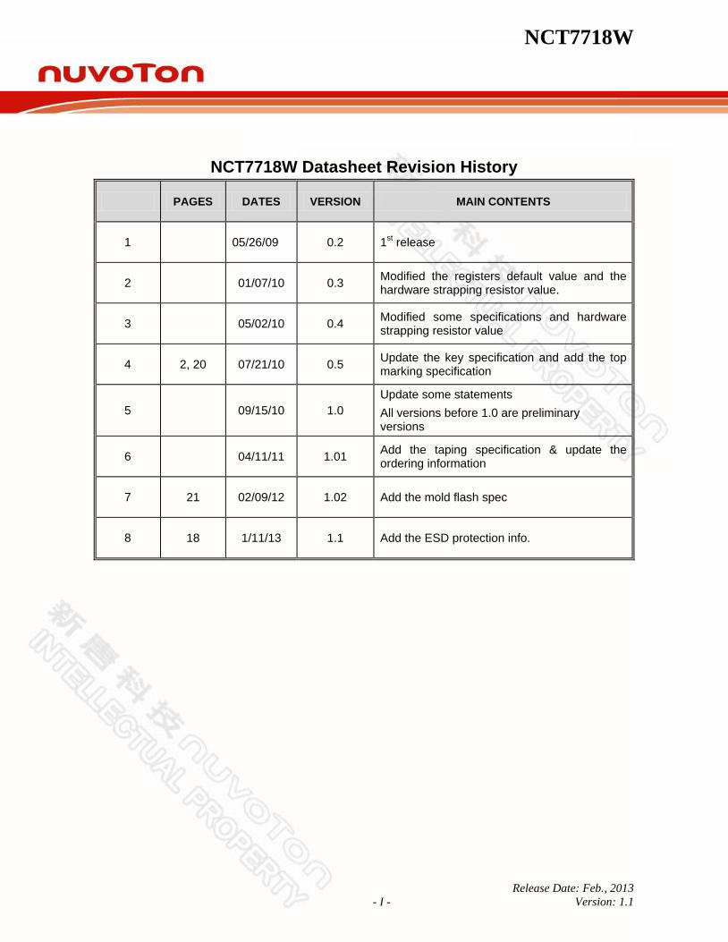
NCT7718W Datasheet Revision History
PAGES DATES VERSION MAIN CONTENTS
1 05/26/09 0.2 1st release
2 01/07/10 0.3 Modified the registers default value and the hardware strapping resistor value.
3 05/02/10 0.4 Modified some specifications and hardware strapping resistor value
4 2, 20 07/21/10 0.5 Update the key specification and add the top marking specification
5 09/15/10 1.0
Update some statements
All versions before 1.0 are preliminary versions
6 04/11/11 1.01 Add the taping specification & update the ordering information
7 21 02/09/12 1.02 Add the mold flash spec
8 18 1/11/13 1.1 Add the ESD protection info.
NCT7718W
Release Date: Feb., 2013
- II - Version: 1.1
Table of Content-
1. GENERAL DESCRIPTION ......................................................................................................... 1
2. FEATURES ................................................................................................................................. 1
2.1 Temperature Measurement ..................................................................................................... 1
2.2 Over Temperature .................................................................................................................... 1
2.3 General ..................................................................................................................................... 1
3. KEY SPECIFICATIONS .............................................................................................................. 2
4. PIN CONFIGURATION ............................................................................................................... 2
5. PIN DESCRIPTION ..................................................................................................................... 3
5.1 PIN TYPE DISCRIPTION ........................................................................................................ 3
5.2 PIN DISCRIPTION ................................................................................................................... 3
6. FUNCTION DESCRIPTION ........................................................................................................ 4
6.1 General Description .................................................................................................................. 4
6.2 Access Interface ....................................................................................................................... 4
6.2.1 Data write to the internal register .............................................................................. 4
6.2.2 Data read from the internal register .......................................................................... 4
6.3 Address Setting ........................................................................................................................ 5
6.4 Temperature Measurement Data Format ................................................................................ 5
6.4.1 The local temperature (on-die) data with 8-bit 2`s complement format. .................... 5
6.4.2 The remote temperature data with 11-bit 2`s complement format. ........................... 5
6.5 ALERT# Output ........................................................................................................................ 6
6.5.1 ALERT# Output Comparator Mode .......................................................................... 6
6.5.2 ALERT# Output Interrupt Mode ................................................................................ 6
6.5.3 ALERT# Output SMBus alert Mode .......................................................................... 7
6.5.4 T_CRIT# Output ....................................................................................................... 7
7. REGISTER SUMMARY .............................................................................................................. 8
7.1 Register Map ............................................................................................................................ 8
7.2 Register Detail .......................................................................................................................... 9
7.2.1 Register: Local Diode Temperature Readout ........................................................... 9
7.2.2 Register: Remote Diode 1 Temperature Readout (MSB) ......................................... 9
7.2.3 Register: Alert Status ................................................................................................ 9
7.2.4 Register: Configuration ........................................................................................... 10
7.2.5 Register: Conversion Rate...................................................................................... 11
7.2.6 Register: Local Diode Temperature Alert Temperature .......................................... 11
7.2.7 Register: Remote Diode 1 Temperature High Alert Temperature (MSB) ................ 11
7.2.8 Register: Remote Diode 1 Temperature Low Alert Temperature (MSB) ................ 12
7.2.9 Register: One Shot Conversion .............................................................................. 12
7.2.10 Register: Remote Diode 1 Temperature Readout (LSB) ........................................ 12
7.2.11 Register: Remote Diode 1 Temperature Offset Register (MSB) ............................. 12
7.2.12 Register: Remote Diode 1 Temperature Offset Register (LSB) .............................. 13
NCT7718W
Release Date: Feb., 2013
- III - Version: 1.1
7.2.13 Register: Remote Diode 1 Temperature High Alert Temperature (LSB) ................. 13
7.2.14 Register: Remote Diode 1 Temperature Low Alert Temperature (LSB) ................. 13
7.2.15 Register: Alert Mask ............................................................................................... 14
7.2.16 Register: Remote Diode 1 Critical Temperature ..................................................... 15
7.2.17 Register: Local Diode Critical Temperature ............................................................ 15
7.2.18 Register: Critical Temperature Hysteresis .............................................................. 16
7.2.19 Register: Customer Data Log Registers ................................................................. 16
7.2.20 Register: Remote Diode Temperature Filter and Alert Mode Setting ...................... 16
7.2.21 Register: Chip ID .................................................................................................... 17
7.2.22 Register: Vendor ID ................................................................................................ 17
7.2.23 Register: Device ID ................................................................................................. 17
8. ELECTRICAL CHARACTERISTICS ......................................................................................... 18
8.1 Absolute Maximum Ratings ................................................................................................... 18
8.2 DC Characteristics ................................................................................................................. 18
8.3 AC Characteristics .................................................................................................................. 19
9. ORDERING INFORMATION ..................................................................................................... 20
10. TOP MARKING SPECIFICATION ............................................................................................ 20
11. TAPING SPECIFICATION ........................................................................................................ 20
12. PACKAGE DRAWING AND DIMENSIONS .............................................................................. 21
NCT7718W
Release Date: Feb., 2013
- 1 - Version: 1.1
1. GENERAL DESCRIPTION
NCT7718W is a temperature sensor with one local and one remote sensor; the remote temperature sensor input could be connected to thermal diode or transistor, such as 2N3904. A 10-bit ADC (Analog-to-Digital Converter) is built inside NCT7718W to convert the monitored temperature value
with 0.125C resolution. Additionally, the NCT7718W supports 2-wire System Management Bus (SMBus
TM) series interface,
and it also provides the hardware thermal alert or system shutdown via ALERT# and T_CRIT# pin.
The NCT7718W is a high precision, low-power consumption IC supporting SMBusTM
interface, which is specifically designed for the PC, Notebook applications, and any embedded environments. Its available package is 8-pin MSOP, with the working voltage of 3.3V.
2. FEATURES
2.1 Temperature Measurement
Measure the temperature with high accuracy
One local on-die thermal sensor
One remote temperature sensor with current mode
2.2 Over Temperature
Supports 2 alert outputs : ALERT# and T_CRIT#
T_CRIT# point supports Hardware Power-on setting
ALERT# output supports SMBusTM
2.0 ARA function
2.3 General
I2C® Compatible System Management bus (SMBus
TM)
3.3V±5% VDD operation
8-pin MSOP Green Package (Halogen-free)
NCT7718W
Release Date: Feb., 2013
- 2 - Version: 1.1
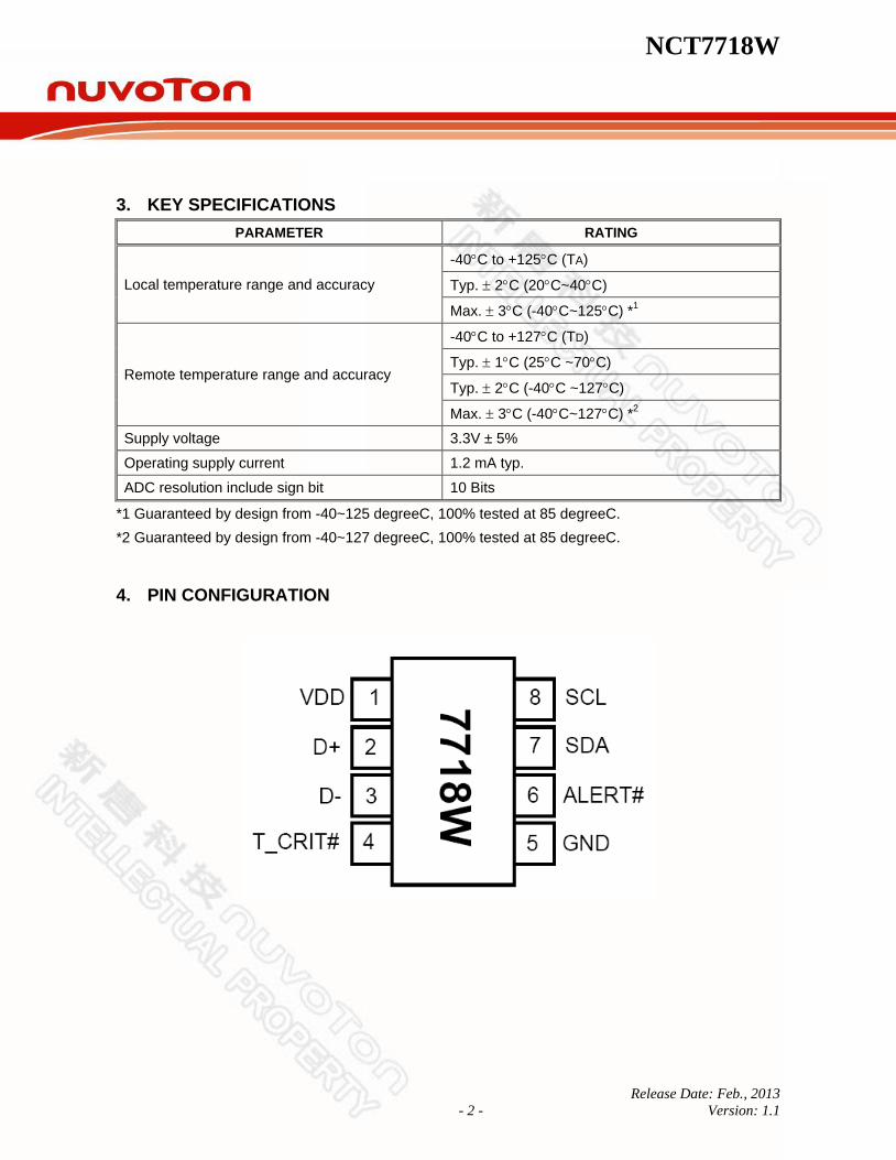
3. KEY SPECIFICATIONS
PARAMETER RATING
Local temperature range and accuracy
-40C to +125C (TA)
Typ. 2C (20C~40C)
Max. 3C (-40C~125C) *1
Remote temperature range and accuracy
-40C to +127C (TD)
Typ. 1C (25C ~70C)
Typ. 2C (-40C ~127C)
Max. 3C (-40C~127C) *2
Supply voltage 3.3V ± 5%
Operating supply current 1.2 mA typ.
ADC resolution include sign bit 10 Bits
*1 Guaranteed by design from -40~125 degreeC, 100% tested at 85 degreeC.
*2 Guaranteed by design from -40~127 degreeC, 100% tested at 85 degreeC.
4. PIN CONFIGURATION
NCT7718W
Release Date: Feb., 2013
- 3 - Version: 1.1
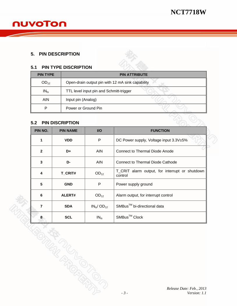
5. PIN DESCRIPTION
5.1 PIN TYPE DISCRIPTION
PIN TYPE PIN ATTRIBUTE
OD12 Open-drain output pin with 12 mA sink capability
INts TTL level input pin and Schmitt-trigger
AIN Input pin (Analog)
P Power or Ground Pin
5.2 PIN DISCRIPTION
PIN NO. PIN NAME I/O FUNCTION
1 VDD P DC Power supply, Voltage input 3.3V±5%
2 D+ AIN Connect to Thermal Diode Anode
3 D- AIN Connect to Thermal Diode Cathode
4 T_CRIT# OD12 T_CRIT alarm output, for interrupt or shutdown control
5 GND P Power supply ground
6 ALERT# OD12 Alarm output, for interrupt control
7 SDA INts/ OD12 SMBusTM
bi-directional data
8 SCL INts SMBusTM
Clock
NCT7718W
Release Date: Feb., 2013
- 4 - Version: 1.1
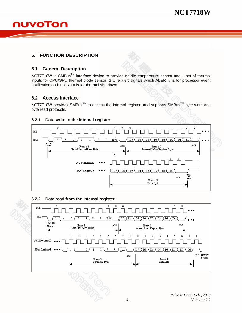
6. FUNCTION DESCRIPTION
6.1 General Description
NCT7718W is SMBusTM
interface device to provide on-die temperature sensor and 1 set of thermal inputs for CPU/GPU thermal diode sensor, 2 wire alert signals which ALERT# is for processor event notification and T_CRIT# is for thermal shutdown.
6.2 Access Interface
NCT7718W provides SMBusTM
to access the internal register, and supports SMBusTM
byte write and byte read protocols.
6.2.1 Data write to the internal register
6.2.2 Data read from the internal register
NCT7718W
Release Date: Feb., 2013
- 5 - Version: 1.1
6.3 Address Setting
NCT7718W I2C/ SMBus
TM address is 1001100xb (x is R/W bit).
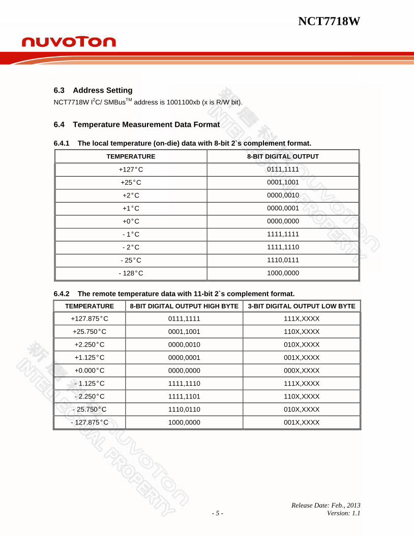
6.4 Temperature Measurement Data Format
6.4.1 The local temperature (on-die) data with 8-bit 2`s complement format.
TEMPERATURE 8-BIT DIGITAL OUTPUT
+127°C 0111,1111
+25°C 0001,1001
+2°C 0000,0010
+1°C 0000,0001
+0°C 0000,0000
- 1°C 1111,1111
- 2°C 1111,1110
- 25°C 1110,0111
- 128°C 1000,0000
6.4.2 The remote temperature data with 11-bit 2`s complement format.
TEMPERATURE 8-BIT DIGITAL OUTPUT HIGH BYTE 3-BIT DIGITAL OUTPUT LOW BYTE
+127.875°C 0111,1111 111X,XXXX
+25.750°C 0001,1001 110X,XXXX
+2.250°C 0000,0010 010X,XXXX
+1.125°C 0000,0001 001X,XXXX
+0.000°C 0000,0000 000X,XXXX
- 1.125°C 1111,1110 111X,XXXX
- 2.250°C 1111,1101 110X,XXXX
- 25.750°C 1110,0110 010X,XXXX
- 127.875°C 1000,0000 001X,XXXX
NCT7718W
Release Date: Feb., 2013
- 6 - Version: 1.1
6.5 ALERT# Output
The NCT7718W ALERT# pin is an active-low open-drain output pin which is triggered when measured temperature exceeds the limitation defined in the limit registers. There are three types of ALERT# output mode: the ALERT# output comparator mode, the ALERT# output interrupt mode, and the ALERT# output SMBus
TM ALERT# mode.
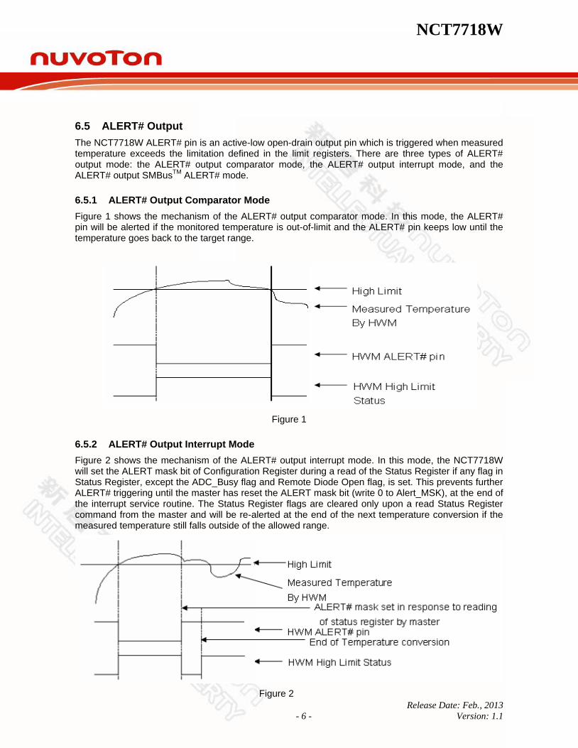
6.5.1 ALERT# Output Comparator Mode
Figure 1 shows the mechanism of the ALERT# output comparator mode. In this mode, the ALERT# pin will be alerted if the monitored temperature is out-of-limit and the ALERT# pin keeps low until the temperature goes back to the target range.
Figure 1
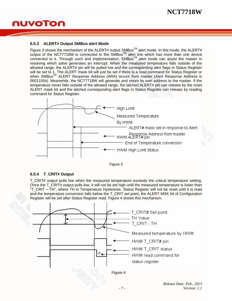
6.5.2 ALERT# Output Interrupt Mode
Figure 2 shows the mechanism of the ALERT# output interrupt mode. In this mode, the NCT7718W will set the ALERT mask bit of Configuration Register during a read of the Status Register if any flag in Status Register, except the ADC_Busy flag and Remote Diode Open flag, is set. This prevents further ALERT# triggering until the master has reset the ALERT mask bit (write 0 to Alert_MSK), at the end of the interrupt service routine. The Status Register flags are cleared only upon a read Status Register command from the master and will be re-alerted at the end of the next temperature conversion if the measured temperature still falls outside of the allowed range.
Figure 2
NCT7718W
Release Date: Feb., 2013
- 7 - Version: 1.1
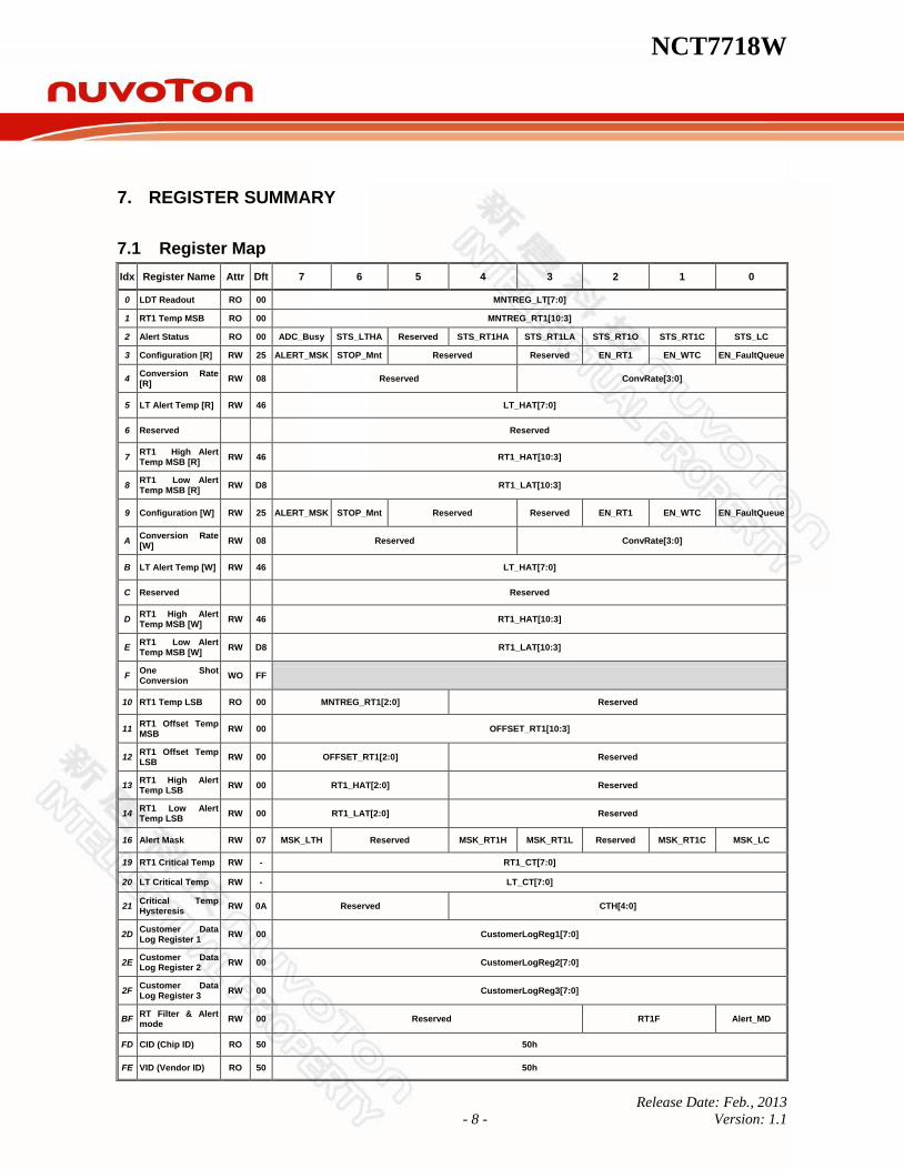
6.5.3 ALERT# Output SMBus alert Mode
Figure 3 shows the mechanism of the ALERT# output SMBusTM
alert mode. In this mode, the ALERT# output of the NCT7718W is connected to the SMBus
TM alert line which has more than one device
connected to it. Through such and implementation, SMBusTM
alert mode can assist the master in resolving which salve generates an interrupt. When the measured temperature falls outside of the allowed range, the ALERT# pin will be pulled low and the corresponding alert flags in Status Register will be set to 1. The ALERT mask bit will just be set if there is a read command for Status Register or when SMBus
TM ALERT Response Address (ARA) occurs from master (Alert Response Address is
0001100x). Meanwhile, the NCT7718W will generate and return its own address to the master. If the temperature never falls outside of the allowed range, the latched ALERT# pin can release by the reset ALERT mask bit and the latched corresponding alert flags in Status Register can release by reading command for Status Register.
Figure 3
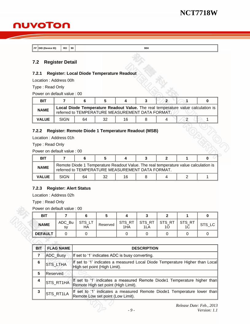
6.5.4 T_CRIT# Output
T_CRIT# output pulls low when the measured temperature exceeds the critical temperature setting. Once the T_CRIT# output pulls low, it will not be set high until the measured temperature is lower than “T_CRIT – TH”, where TH is Temperature Hysteresis. Status Register will not be reset until it is read and the temperature conversion falls below the T_CRIT set point, the ALERT-MSK bit of Configuration Register will be set after Status Register read. Figure 4 shows this mechanism.
Figure 4
NCT7718W
Release Date: Feb., 2013
- 8 - Version: 1.1
7. REGISTER SUMMARY
7.1 Register Map
Idx Register Name Attr Dft 7 6 5 4 3 2 1 0
0 LDT Readout RO 00 MNTREG_LT[7:0]
1 RT1 Temp MSB RO 00 MNTREG_RT1[10:3]
2 Alert Status RO 00 ADC_Busy STS_LTHA Reserved STS_RT1HA STS_RT1LA STS_RT1O STS_RT1C STS_LC
3 Configuration [R] RW 25 ALERT_MSK STOP_Mnt Reserved Reserved EN_RT1 EN_WTC EN_FaultQueue
4 Conversion Rate [R]
RW 08 Reserved ConvRate[3:0]
5 LT Alert Temp [R] RW 46 LT_HAT[7:0]
6 Reserved Reserved
7 RT1 High Alert Temp MSB [R]
RW 46 RT1_HAT[10:3]
8 RT1 Low Alert Temp MSB [R]
RW D8 RT1_LAT[10:3]
9 Configuration [W] RW 25 ALERT_MSK STOP_Mnt Reserved Reserved EN_RT1 EN_WTC EN_FaultQueue
A Conversion Rate [W]
RW 08 Reserved ConvRate[3:0]
B LT Alert Temp [W] RW 46 LT_HAT[7:0]
C Reserved Reserved
D RT1 High Alert Temp MSB [W]
RW 46 RT1_HAT[10:3]
E RT1 Low Alert Temp MSB [W]
RW D8 RT1_LAT[10:3]
F One Shot Conversion
WO FF
10 RT1 Temp LSB RO 00 MNTREG_RT1[2:0] Reserved
11 RT1 Offset Temp MSB
RW 00 OFFSET_RT1[10:3]
12 RT1 Offset Temp LSB
RW 00 OFFSET_RT1[2:0] Reserved
13 RT1 High Alert Temp LSB
RW 00 RT1_HAT[2:0] Reserved
14 RT1 Low Alert Temp LSB
RW 00 RT1_LAT[2:0] Reserved
16 Alert Mask RW 07 MSK_LTH Reserved MSK_RT1H MSK_RT1L Reserved MSK_RT1C MSK_LC
19 RT1 Critical Temp RW - RT1_CT[7:0]
20 LT Critical Temp RW - LT_CT[7:0]
21 Critical Temp Hysteresis
RW 0A Reserved CTH[4:0]
2D Customer Data Log Register 1
RW 00 CustomerLogReg1[7:0]
2E Customer Data Log Register 2
RW 00 CustomerLogReg2[7:0]
2F Customer Data Log Register 3
RW 00 CustomerLogReg3[7:0]
BF RT Filter & Alert mode
RW 00 Reserved RT1F Alert_MD
FD CID (Chip ID) RO 50 50h
FE VID (Vendor ID) RO 50 50h
NCT7718W
Release Date: Feb., 2013
- 9 - Version: 1.1
FF DID (Device ID) RO 90 90H
7.2 Register Detail
7.2.1 Register: Local Diode Temperature Readout
Location : Address 00h
Type : Read Only
Power on default value : 00
BIT 7 6 5 4 3 2 1 0
NAME Local Diode Temperature Readout Value. The real temperature value calculation is referred to TEMPERATURE MEASUREMENT DATA FORMAT.
VALUE SIGN 64 32 16 8 4 2 1
7.2.2 Register: Remote Diode 1 Temperature Readout (MSB)
Location : Address 01h
Type : Read Only
Power on default value : 00
BIT 7 6 5 4 3 2 1 0
NAME Remote Diode 1 Temperature Readout Value. The real temperature value calculation is referred to TEMPERATURE MEASUREMENT DATA FORMAT.
VALUE SIGN 64 32 16 8 4 2 1
7.2.3 Register: Alert Status
Location : Address 02h
Type : Read Only
Power on default value : 00
BIT 7 6 5 4 3 2 1 0
NAME ADC_Bu
sy STS_LT
HA Reserved
STS_RT1HA
STS_RT1LA
STS_RT1O
STS_RT1C
STS_LC
DEFAULT 0 0 0 0 0 0 0
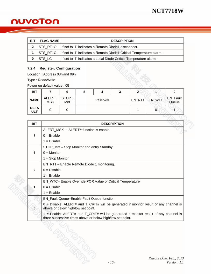
BIT FLAG NAME DESCRIPTION
7 ADC_Busy If set to „1‟ indicates ADC is busy converting.
6 STS_LTHA
If set to „1‟ indicates a measured Local Diode Temperature Higher than Local High set point (High Limit).
5 Reserved
4 STS_RT1HA
If set to „1‟ indicates a measured Remote Diode1 Temperature higher than Remote High set point (High Limit).
3 STS_RT1LA
If set to „1‟ indicates a measured Remote Diode1 Temperature lower than Remote Low set point (Low Limit).
NCT7718W
Release Date: Feb., 2013
- 10 - Version: 1.1
BIT FLAG NAME DESCRIPTION
2 STS_RT1O If set to „1‟ indicates a Remote Diode1 disconnect.
1 STS_RT1C If set to „1‟ indicates a Remote Diode1 Critical Temperature alarm.
0 STS_LC If set to „1‟ indicates a Local Diode Critical Temperature alarm.
7.2.4 Register: Configuration
Location : Address 03h and 09h
Type : Read/Write
Power on default value : 05
BIT 7 6 5 4 3 2 1 0
NAME ALERT_
MSK STOP_
Mnt Reserved EN_RT1 EN_WTC
EN_FaultQueue
DEFAULT
0 0 1 0 1
BIT DESCRIPTION
7
ALERT_MSK –. ALERT# function is enable
0 = Enable
1 = Disable
6
STOP_Mnt – Stop Monitor and entry Standby
0 = Monitor
1 = Stop Monitor
2
EN_RT1 – Enable Remote Diode 1 monitoring.
0 = Disable
1 = Enable
1
EN_WTC– Enable Override POR Value of Critical Temperature
0 = Disable
1 = Enable
0
EN_Fault Queue–Enable Fault Queue function.
0 = Disable. ALERT# and T_CRIT# will be generated if monitor result of any channel is above or below high/low set point.
1 = Enable. ALERT# and T_CRIT# will be generated if monitor result of any channel is three successive times above or below high/low set point.
NCT7718W
Release Date: Feb., 2013
- 11 - Version: 1.1
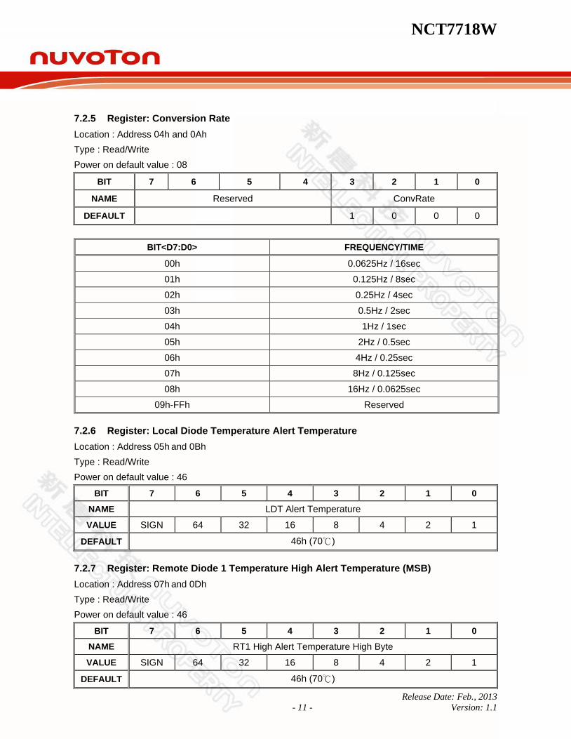
7.2.5 Register: Conversion Rate
Location : Address 04h and 0Ah
Type : Read/Write
Power on default value : 08
BIT 7 6 5 4 3 2 1 0
NAME Reserved ConvRate
DEFAULT 1 0 0 0
BIT<D7:D0> FREQUENCY/TIME
00h 0.0625Hz / 16sec
01h 0.125Hz / 8sec
02h 0.25Hz / 4sec
03h 0.5Hz / 2sec
04h 1Hz / 1sec
05h 2Hz / 0.5sec
06h 4Hz / 0.25sec
07h 8Hz / 0.125sec
08h 16Hz / 0.0625sec
09h-FFh Reserved
7.2.6 Register: Local Diode Temperature Alert Temperature
Location : Address 05h and 0Bh
Type : Read/Write
Power on default value : 46
BIT 7 6 5 4 3 2 1 0
NAME LDT Alert Temperature
VALUE SIGN 64 32 16 8 4 2 1
DEFAULT 46h (70℃)
7.2.7 Register: Remote Diode 1 Temperature High Alert Temperature (MSB)
Location : Address 07h and 0Dh
Type : Read/Write
Power on default value : 46
BIT 7 6 5 4 3 2 1 0
NAME RT1 High Alert Temperature High Byte
VALUE SIGN 64 32 16 8 4 2 1
DEFAULT 46h (70℃)
NCT7718W
Release Date: Feb., 2013
- 12 - Version: 1.1
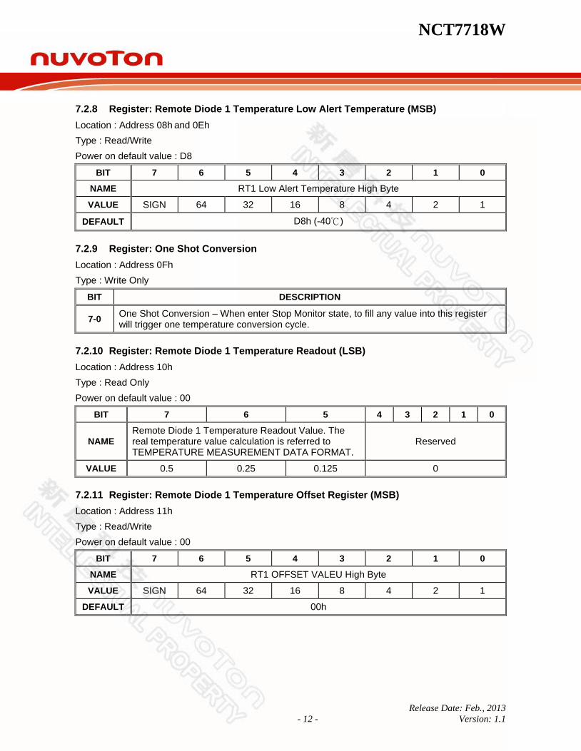
7.2.8 Register: Remote Diode 1 Temperature Low Alert Temperature (MSB)
Location : Address 08h and 0Eh
Type : Read/Write
Power on default value : D8
BIT 7 6 5 4 3 2 1 0
NAME RT1 Low Alert Temperature High Byte
VALUE SIGN 64 32 16 8 4 2 1
DEFAULT D8h (-40℃)
7.2.9 Register: One Shot Conversion
Location : Address 0Fh
Type : Write Only
BIT DESCRIPTION
7-0 One Shot Conversion – When enter Stop Monitor state, to fill any value into this register will trigger one temperature conversion cycle.
7.2.10 Register: Remote Diode 1 Temperature Readout (LSB)
Location : Address 10h
Type : Read Only
Power on default value : 00
BIT 7 6 5 4 3 2 1 0
NAME
Remote Diode 1 Temperature Readout Value. The real temperature value calculation is referred to TEMPERATURE MEASUREMENT DATA FORMAT.
Reserved
VALUE 0.5 0.25 0.125 0
7.2.11 Register: Remote Diode 1 Temperature Offset Register (MSB)
Location : Address 11h
Type : Read/Write
Power on default value : 00
BIT 7 6 5 4 3 2 1 0
NAME RT1 OFFSET VALEU High Byte
VALUE SIGN 64 32 16 8 4 2 1
DEFAULT 00h
NCT7718W
Release Date: Feb., 2013
- 13 - Version: 1.1
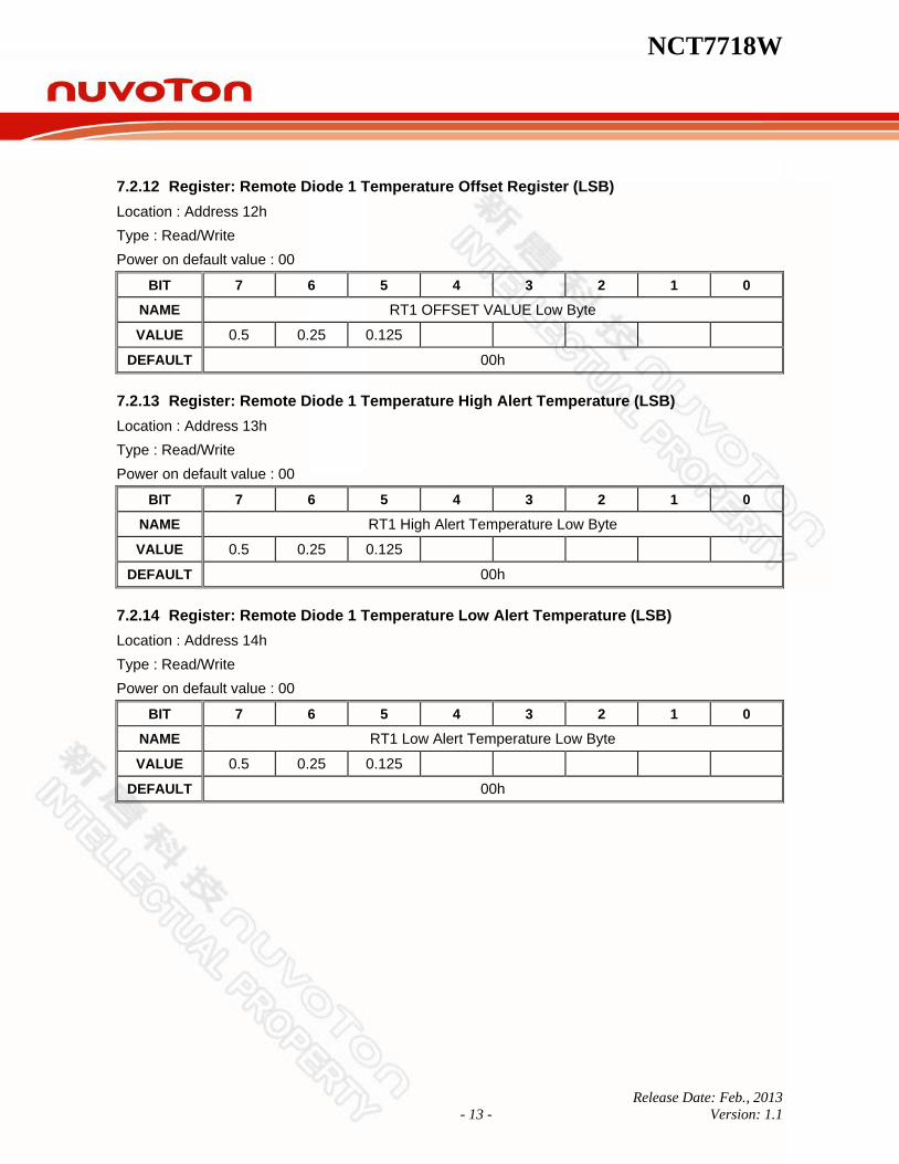
7.2.12 Register: Remote Diode 1 Temperature Offset Register (LSB)
Location : Address 12h
Type : Read/Write
Power on default value : 00
BIT 7 6 5 4 3 2 1 0
NAME RT1 OFFSET VALUE Low Byte
VALUE 0.5 0.25 0.125
DEFAULT 00h
7.2.13 Register: Remote Diode 1 Temperature High Alert Temperature (LSB)
Location : Address 13h
Type : Read/Write
Power on default value : 00
BIT 7 6 5 4 3 2 1 0
NAME RT1 High Alert Temperature Low Byte
VALUE 0.5 0.25 0.125
DEFAULT 00h
7.2.14 Register: Remote Diode 1 Temperature Low Alert Temperature (LSB)
Location : Address 14h
Type : Read/Write
Power on default value : 00
BIT 7 6 5 4 3 2 1 0
NAME RT1 Low Alert Temperature Low Byte
VALUE 0.5 0.25 0.125
DEFAULT 00h
NCT7718W
Release Date: Feb., 2013
- 14 - Version: 1.1
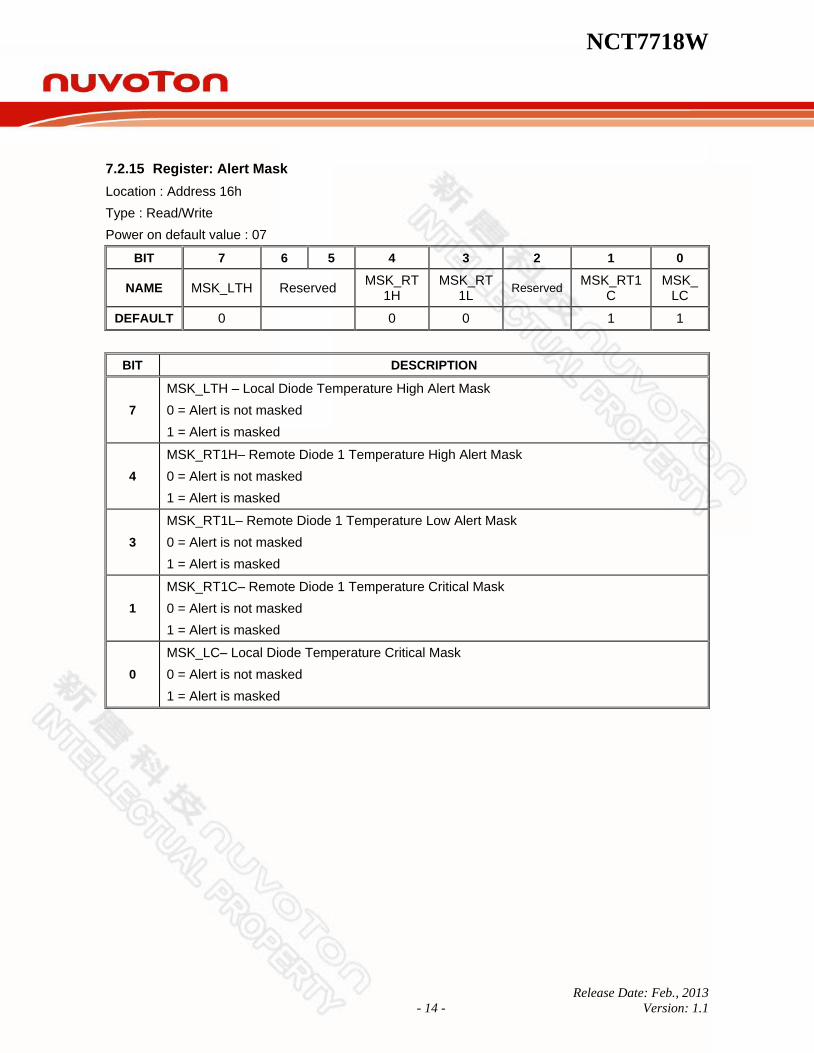
7.2.15 Register: Alert Mask
Location : Address 16h
Type : Read/Write
Power on default value : 07
BIT 7 6 5 4 3 2 1 0
NAME MSK_LTH Reserved MSK_RT
1H MSK_RT
1L Reserved
MSK_RT1C
MSK_LC
DEFAULT 0 0 0 1 1
BIT DESCRIPTION
7
MSK_LTH – Local Diode Temperature High Alert Mask
0 = Alert is not masked
1 = Alert is masked
4
MSK_RT1H– Remote Diode 1 Temperature High Alert Mask
0 = Alert is not masked
1 = Alert is masked
3
MSK_RT1L– Remote Diode 1 Temperature Low Alert Mask
0 = Alert is not masked
1 = Alert is masked
1
MSK_RT1C– Remote Diode 1 Temperature Critical Mask
0 = Alert is not masked
1 = Alert is masked
0
MSK_LC– Local Diode Temperature Critical Mask
0 = Alert is not masked
1 = Alert is masked
NCT7718W
Release Date: Feb., 2013
- 15 - Version: 1.1
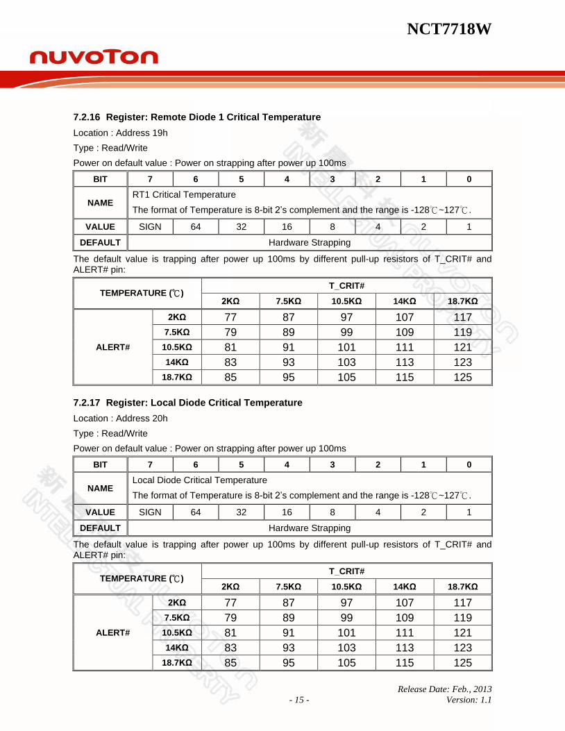
7.2.16 Register: Remote Diode 1 Critical Temperature
Location : Address 19h
Type : Read/Write
Power on default value : Power on strapping after power up 100ms
BIT 7 6 5 4 3 2 1 0
NAME RT1 Critical Temperature
The format of Temperature is 8-bit 2‟s complement and the range is -128℃~127℃.
VALUE SIGN 64 32 16 8 4 2 1
DEFAULT Hardware Strapping
The default value is trapping after power up 100ms by different pull-up resistors of T_CRIT# and ALERT# pin:
TEMPERATURE (℃) T_CRIT#
2KΩ 7.5KΩ 10.5KΩ 14KΩ 18.7KΩ
ALERT#
2KΩ 77 87 97 107 117
7.5KΩ 79 89 99 109 119
10.5KΩ 81 91 101 111 121
14KΩ 83 93 103 113 123
18.7KΩ 85 95 105 115 125
7.2.17 Register: Local Diode Critical Temperature
Location : Address 20h
Type : Read/Write
Power on default value : Power on strapping after power up 100ms
BIT 7 6 5 4 3 2 1 0
NAME Local Diode Critical Temperature
The format of Temperature is 8-bit 2‟s complement and the range is -128℃~127℃.
VALUE SIGN 64 32 16 8 4 2 1
DEFAULT Hardware Strapping
The default value is trapping after power up 100ms by different pull-up resistors of T_CRIT# and ALERT# pin:
TEMPERATURE (℃) T_CRIT#
2KΩ 7.5KΩ 10.5KΩ 14KΩ 18.7KΩ
ALERT#
2KΩ 77 87 97 107 117
7.5KΩ 79 89 99 109 119
10.5KΩ 81 91 101 111 121
14KΩ 83 93 103 113 123
18.7KΩ 85 95 105 115 125
NCT7718W
Release Date: Feb., 2013
- 16 - Version: 1.1
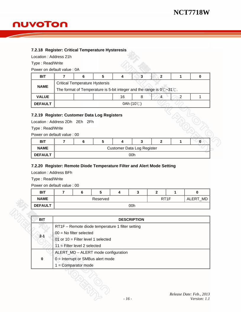
7.2.18 Register: Critical Temperature Hysteresis
Location : Address 21h
Type : Read/Write
Power on default value : 0A
BIT 7 6 5 4 3 2 1 0
NAME Critical Temperature Hystersis
The format of Temperature is 5-bit integer and the range is 0℃~31℃.
VALUE 16 8 4 2 1
DEFAULT 0Ah (10℃)
7.2.19 Register: Customer Data Log Registers
Location : Address 2Dh 2Eh 2Fh
Type : Read/Write
Power on default value : 00
BIT 7 6 5 4 3 2 1 0
NAME Customer Data Log Register
DEFAULT 00h
7.2.20 Register: Remote Diode Temperature Filter and Alert Mode Setting
Location : Address BFh
Type : Read/Write
Power on default value : 00
BIT 7 6 5 4 3 2 1 0
NAME Reserved RT1F ALERT_MD
DEFAULT 00h
BIT DESCRIPTION
2-1
RT1F – Remote diode temperature 1 filter setting
00 = No filter selected
01 or 10 = Filter level 1 selected
11 = Filter level 2 selected
0
ALERT_MD – ALERT mode configuration
0 = Interrupt or SMBus alert mode
1 = Comparator mode
NCT7718W
Release Date: Feb., 2013
- 17 - Version: 1.1
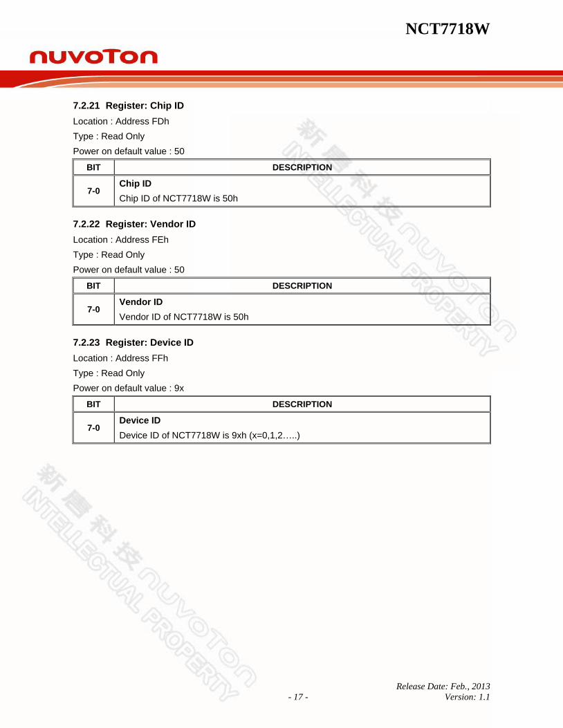
7.2.21 Register: Chip ID
Location : Address FDh
Type : Read Only
Power on default value : 50
BIT DESCRIPTION
7-0 Chip ID
Chip ID of NCT7718W is 50h
7.2.22 Register: Vendor ID
Location : Address FEh
Type : Read Only
Power on default value : 50
BIT DESCRIPTION
7-0 Vendor ID
Vendor ID of NCT7718W is 50h
7.2.23 Register: Device ID
Location : Address FFh
Type : Read Only
Power on default value : 9x
BIT DESCRIPTION
7-0 Device ID
Device ID of NCT7718W is 9xh (x=0,1,2…..)
NCT7718W
Release Date: Feb., 2013
- 18 - Version: 1.1
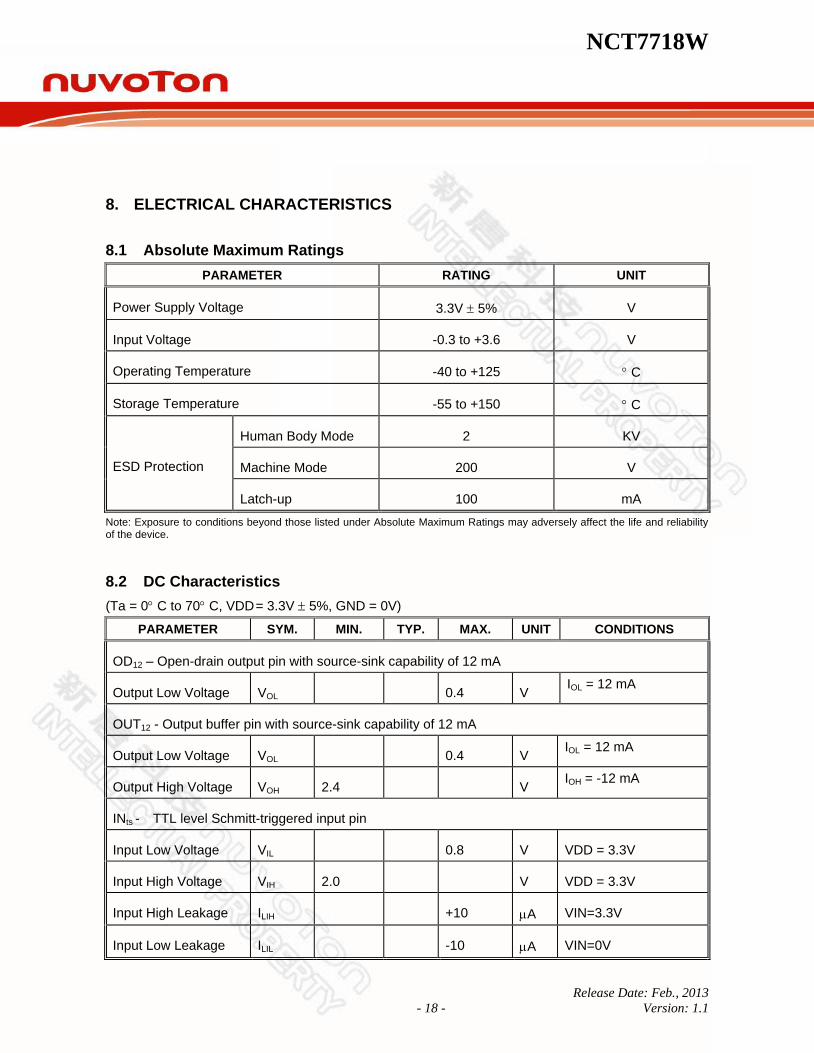
8. ELECTRICAL CHARACTERISTICS
8.1 Absolute Maximum Ratings
PARAMETER RATING UNIT
Power Supply Voltage 3.3V 5% V
Input Voltage -0.3 to +3.6 V
Operating Temperature -40 to +125 C
Storage Temperature -55 to +150 C
ESD Protection
Human Body Mode 2 KV
Machine Mode 200 V
Latch-up 100 mA
Note: Exposure to conditions beyond those listed under Absolute Maximum Ratings may adversely affect the life and reliability of the device.
8.2 DC Characteristics
(Ta = 0 C to 70 C, VDD = 3.3V 5%, GND = 0V)
PARAMETER SYM. MIN. TYP. MAX. UNIT CONDITIONS
OD12 – Open-drain output pin with source-sink capability of 12 mA
Output Low Voltage VOL 0.4 V IOL = 12 mA
OUT12 - Output buffer pin with source-sink capability of 12 mA
Output Low Voltage VOL 0.4 V IOL = 12 mA
Output High Voltage VOH 2.4 V IOH = -12 mA
INts - TTL level Schmitt-triggered input pin
Input Low Voltage VIL 0.8 V VDD = 3.3V
Input High Voltage VIH 2.0 V VDD = 3.3V
Input High Leakage ILIH +10 A VIN=3.3V
Input Low Leakage ILIL -10 A VIN=0V
NCT7718W
Release Date: Feb., 2013
- 19 - Version: 1.1
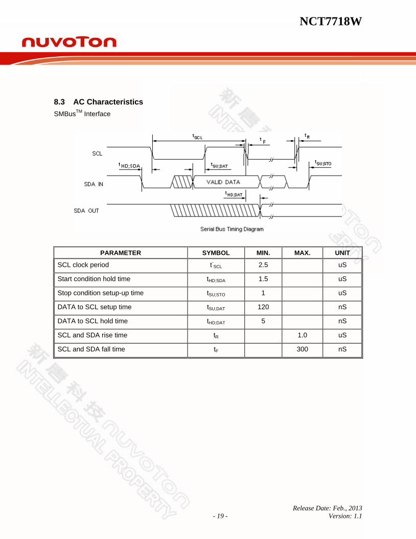
8.3 AC Characteristics
SMBusTM
Interface
PARAMETER SYMBOL MIN. MAX. UNIT
SCL clock period t-SCL 2.5 uS
Start condition hold time tHD;SDA 1.5 uS
Stop condition setup-up time tSU;STO 1 uS
DATA to SCL setup time tSU;DAT 120 nS
DATA to SCL hold time tHD;DAT 5 nS
SCL and SDA rise time tR 1.0 uS
SCL and SDA fall time tF 300 nS
NCT7718W
Release Date: Feb., 2013
- 20 - Version: 1.1
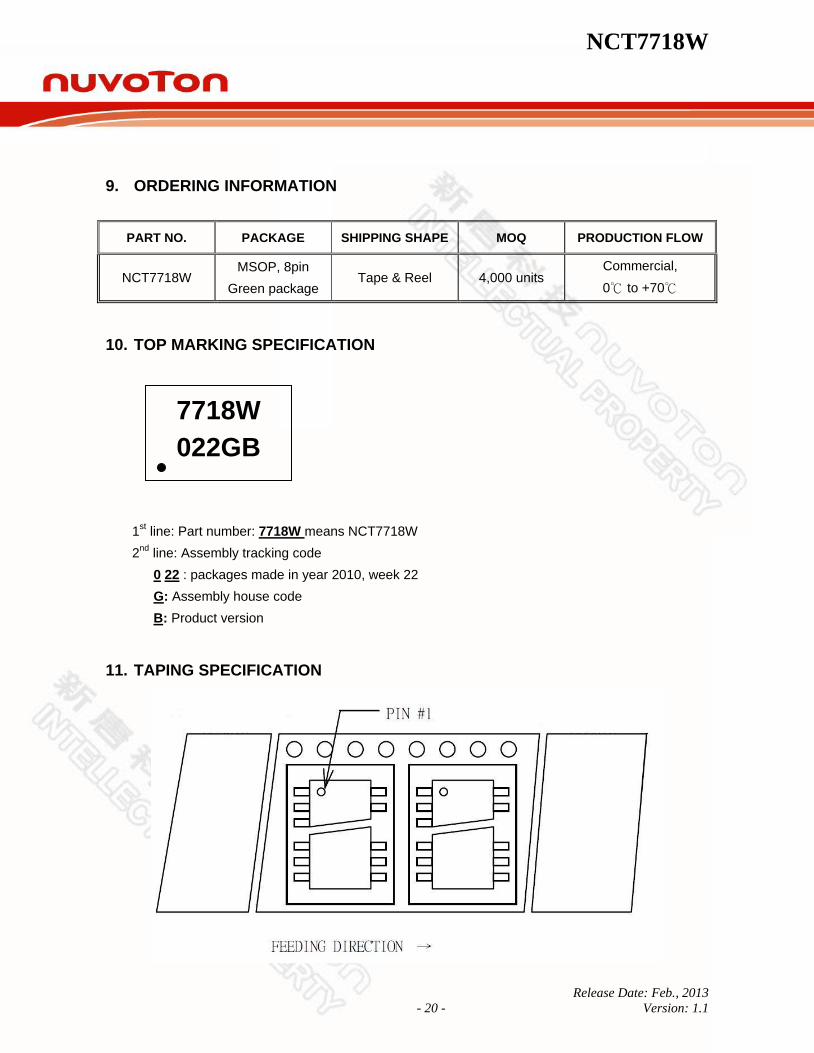
9. ORDERING INFORMATION
PART NO. PACKAGE SHIPPING SHAPE MOQ PRODUCTION FLOW
NCT7718W MSOP, 8pin
Green package Tape & Reel 4,000 units
Commercial,
0℃ to +70℃
10. TOP MARKING SPECIFICATION
1st line: Part number: 7718W means NCT7718W
2nd
line: Assembly tracking code
0 22 : packages made in year 2010, week 22
G: Assembly house code
B: Product version
11. TAPING SPECIFICATION
7718W
022GB
NCT7718W
Release Date: Feb., 2013
- 21 - Version: 1.1
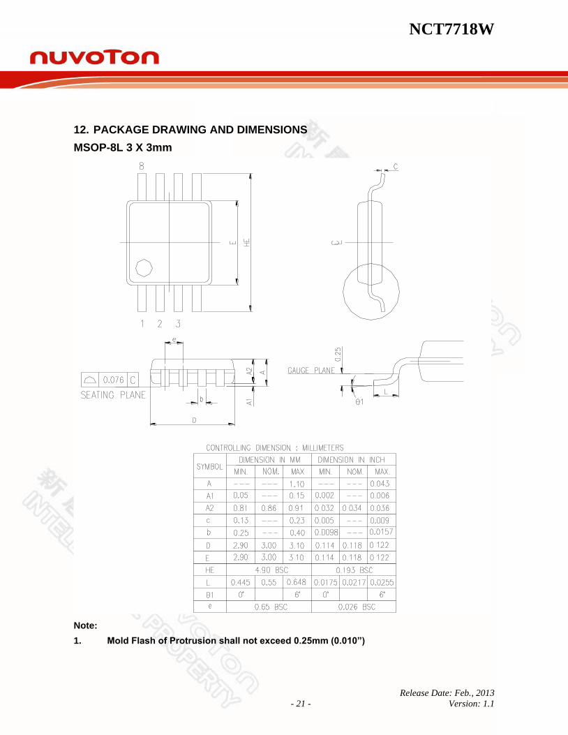
12. PACKAGE DRAWING AND DIMENSIONS
MSOP-8L 3 X 3mm
Note:
1. Mold Flash of Protrusion shall not exceed 0.25mm (0.010”)
NCT7718W
Release Date: Feb., 2013
- 22 - Version: 1.1
Important Notice
Nuvoton Products are neither intended nor warranted for usage in systems or equipment, any malfunction or failure of which may cause loss of human life, bodily injury or severe property damage. Such applications are deemed, “Insecure Usage”.
Insecure usage includes, but is not limited to: equipment for surgical implementation, atomic energy control instruments, airplane or spaceship instruments, the control or operation of dynamic, brake or safety systems designed for vehicular use, traffic signal instruments, all types of safety devices, and other applications intended to support or sustain life.
All Insecure Usage shall be made at customer’s risk, and in the event that third parties lay claims to Nuvoton as a result of customer’s Insecure Usage, customer shall indemnify the damages and liabilities thus incurred by Nuvoton.