Embed Size (px)
Citation preview

© Semiconductor Components Industries, LLC, 2016
March, 2016 − Rev. 71 Publication Order Number:
NCP81022/D
NCP81022
Dual Output 4 Phase Plus 1Phase Digital Controllerwith SVI2 Interface forDesktop and Notebook CPUApplications
The NCP81022 dual output four plus one phase buck solution isoptimized for AMD® SVI2 CPUs. The controller combines truedifferential voltage sensing, differential inductor DCR currentsensing, input voltage feed−forward, and adaptive voltage positioningto provide accurately regulated power for both desktop and notebookapplications.
The control system is based on Dual−Edge pulse−width modulation(PWM) combined with DCR current sensing providing an ultra fastinitial response to dynamic load events and reduced system cost. TheNCP81022 provides the mechanism to shed to single phase duringlight load operation and can auto frequency scale in light loadconditions while maintaining excellent transient performance.
Dual high performance operational error amplifiers are provided tosimplify compensation of the system. Patented Dynamic ReferenceInjection further simplifies loop compensation by eliminating the needto compromise between closed−loop transient response and DynamicVID performance. Patented Total Current Summing provides highlyaccurate current monitoring for droop and digital current monitoring.
Features• Meets AMD’S SVI2 Specifications
• Four phase CPU Voltage Regulator
• One phase North Bridge Voltage Regulator
• Current Mode Dual Edge Modulation for Fast Initial Response toTransient Loading
• Dual High Performance Operational Error Amplifier
• One Digital Soft Start Ramp for Both Rails
• Dynamic Reference Injection
• Accurate Total Summing Current Amplifier
• DAC with Droop Feed−forward Injection
• Dual High Impedance Differential Voltage and TotalCurrent Sense Amplifiers
• Phase−to−Phase Dynamic Current Balancing
• “Lossless” DCR Current Sensing for Current Balancing
• Summed Compensated Inductor Current Sensing forDroop
• True Differential Current Balancing Sense Amplifiersfor Each Phase
• Adaptive Voltage Positioning (AVP)
• Switching Frequency Range of 240 kHz – 1.0 MHz
• Startup into Pre−Charged Loads while avoiding FalseOVP
• Power Saving Phase Shedding
• Vin Feed Forward Ramp Slope
• Pin Programming for Internal SVI2 Parameters
• Over Voltage Protection (OVP) and Under VoltageProtection (UVP)
• Over Current Protection (OCP)
• Dual Power Good Output with Internal Delays
• These Devices are Pb−Free and Halogen Free
Applications• Desktop and Notebook Processors
• Gaming
MARKINGDIAGRAM
www.onsemi.com
See detailed ordering and shipping information on page 40 ofthis data sheet.
ORDERING INFORMATION
521
QFN52CASE 485BE
A = Assembly LocationWL = Wafer LotYY = YearWW = Work WeekG = Pb−Free Package
NCP81022AWLYYWWG

NCP81022
www.onsemi.com2
UVLO & EN
OVER CURRENT
PROTECTION
SVI2INTERFACE
EN
GND
VCC
OCP_L
SVD
SVC
SVT
VDDNB_PWRGD
VDD_PWRGDVDD_PWRGD
COMPARATOR
VDDNB_PWRGD
COMPARATOR
DAC
GND
CSREF
VSS
VDDNB
DROOPNB
DIFFAMP
NORTH
BRIDGE
FBNB
COMPNB
TRBSTNB
TRBSTCONTROL
NORTH
BRIDGE
CSSUMNB
CSCOMPNB
ILIMNB ILIM
IOUTNORTH BRIDGE
CURRENT
BALANCE
CSP1NB
CSN1NB
NORTH
BRIDGEMAINRAIL
PHASEGENERATOR
RAMP
GENERATORS
PWMGENERATOR
CURRENT
BALANCE
DAC
GND
CSREF
DIFFAMP
DIFF
ILIM
IOUT
FB
COMP
CSP1
CSP2
ILIM
CSCOMP
CSREF
CSSUM
PWM2
VR
MP
PW
M1N
B
TRANSIENT
CONTROL
ENABLE
OVP
NORTH BRIDGE
OVP
OVP_NB
OVP
ADCMUX
VBOOTDAC
DAC
DAC
NB_DAC
ENABLE
VSS_SENSE
VDD_SENSEDAC
DROOP
VSS_SENSEVDDNB_SENSE
NB_DACENABLE
VDD_SENSE
VSS_SENSE
VDDNB_SENSE
ENABLE
ENABLE
ENABLENB
COMPNNB
OVPNB
ENABLECOMP
OVP
RMPNB
RAMP1
RAMP2
CSAMP
ERROR
AMP_NB
CSAMP
ERROR
AMP
VDD
VSSVDDNB − VSS_SENSEVDD −VSS_SENSE
DROOP
DR
ON
VDDIO
DIFFNB
IOUTNB
IOUT
IMAXIMAXNB
SRSRNB
CSN 1NB
RAMP3
RAMP4
PWM1
PWM3
PWM4
CSN1
CSN2
CSP3
CSN3
CSP4
CSN4
TRBST
ENABLE_NB
ENABLE_NB
ENABLE_NB
SDA SCL
DIGITAL
INTERFACE
Digital Config and
value registers
NCP81022
Figure 1. Block Diagram
NCP81022
www.onsemi.com3
NCP81022
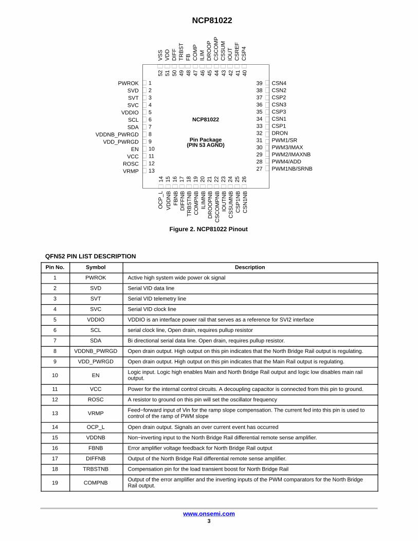
Pin Package
12345678910111213
14 15 16 17 18 19 20 21 22 23 24 25 26
PWROK CSN4
OC
P_L
VD
DN
BF
BN
BD
IFF
NB
TR
BS
TN
BC
OM
PN
BIL
IMN
BD
RO
OP
NB
CS
CO
MP
NB
IOU
TN
BC
SS
UM
NB
CS
P1N
BC
SN
1NB
VS
SV
DD
DIF
FT
RB
ST
FB
CO
MP
ILIM
DR
OO
PC
SC
OM
PC
SS
UM
IOU
TC
SR
EF
CS
P4
52 51 50 49 48 47 46 45 44 43 42 41 40
39383736353433323130292827
(PIN 53 AGND)
SVDSVTSVC
VDDIOSCLSDA
VDDNB_PWRGDVDD_PWRGD
ENVCC
ROSCVRMP
CSN2CSP2CSN3CSP3CSN1CSP1DRONPWM1/SRPWM3/IMAXPWM2/IMAXNBPWM4/ADDPWM1NB/SRNB
Figure 2. NCP81022 Pinout
QFN52 PIN LIST DESCRIPTION
Pin No. Symbol Description
1 PWROK Active high system wide power ok signal
2 SVD Serial VID data line
3 SVT Serial VID telemetry line
4 SVC Serial VID clock line
5 VDDIO VDDIO is an interface power rail that serves as a reference for SVI2 interface
6 SCL serial clock line, Open drain, requires pullup resistor
7 SDA Bi directional serial data line. Open drain, requires pullup resistor.
8 VDDNB_PWRGD Open drain output. High output on this pin indicates that the North Bridge Rail output is regulating.
9 VDD_PWRGD Open drain output. High output on this pin indicates that the Main Rail output is regulating.
10 ENLogic input. Logic high enables Main and North Bridge Rail output and logic low disables main railoutput.
11 VCC Power for the internal control circuits. A decoupling capacitor is connected from this pin to ground.
12 ROSC A resistor to ground on this pin will set the oscillator frequency
13 VRMPFeed−forward input of Vin for the ramp slope compensation. The current fed into this pin is used tocontrol of the ramp of PWM slope
14 OCP_L Open drain output. Signals an over current event has occurred
15 VDDNB Non−inverting input to the North Bridge Rail differential remote sense amplifier.
16 FBNB Error amplifier voltage feedback for North Bridge Rail output
17 DIFFNB Output of the North Bridge Rail differential remote sense amplifier.
18 TRBSTNB Compensation pin for the load transient boost for North Bridge Rail
19 COMPNBOutput of the error amplifier and the inverting inputs of the PWM comparators for the North BridgeRail output.

NCP81022
www.onsemi.com4
QFN52 PIN LIST DESCRIPTION
Pin No. DescriptionSymbol
20 ILIMNBOver current shutdown threshold setting for North Bridge Rail output. Resistor to CSCOMP to setthreshold.
21 DROOPNBUsed to program DACFF function for North Bridge Rail output. It’s connected to the resistor dividerplaced between CSCOMPNB and CSREFNB summing node.
22 CSCOMPNB Output of total current sense amplifier for North Bridge Rail output.
23 IOUTNB Total output current monitor for North Bridge Rail.
24 CSSUMNB Inverting input of total current sense amplifier for North Bridge Rail output.
25 CSP1NB Non−inverting input to current balance sense amplifier for phase 1NB
26 CSN1NB Inverting input to current balance sense amplifier for phase1NB
27 PWM1NB/SRNB North Bridge Phase1 PWM output. A resistor from this pin to ground programs SR North Bridge rail
28 PWM4/ADD Main Rail Phase 4PWM output. A resistor from this pin to ground programs the SMBus address.
29 PWM2/IMAXNBMain Rail Phase 2PWM output. During start up it is used to program ICC_MAX for the North BridgeRail with a resistor to ground
30 PWM3/IMAXMain Rail Phase 3PWM output. During start up it is used to program ICC_MAX for the Main Rail witha resistor to ground
31 PWM1/SR Main Rail Phase 1PWM output. A resistor to ground on this pin programs SR Main rail.
32 DRONBidirectional gate driver enable for external drivers for both Main and North Bridge Rails. It should beleft floating if unused.
33 CSP1 Non−inverting input to current balance sense amplifier for Main Rail phase 1
34 CSN1 Non−inverting input to current balance sense amplifier for Main Rail phase 1
35 CSP3 Non−inverting input to current balance sense amplifier for Main Rail phase 3
36 CSN3 Inverting input to current balance sense amplifier for Main Rail phase3
37 CSP2 Non−inverting input to current balance sense amplifier for Main Rail phase 2
38 CSN2 Inverting input to current balance sense amplifier for Main Rail phase2
39 CSN4 Inverting input to current balance sense amplifier for Main Rail phase4
40 CSP4 Non−inverting input to current balance sense amplifier for Main Rail phase 4
41 CSREFTotal output current sense amplifier reference voltage input for Main Rail and inverting input to MainRail current balance sense amplifier for phase 1 and 2
42 IOUT Total output current monitor for Main Rail.
43 CSSUM Inverting input of total current sense amplifier for Main Rail output
44 CSCOMP Output of total current sense amplifier for Main Rail output
45 DROOPUsed to program DACFF function for Main Rail output. It’s connected to the resistor divider placedbetween CSCOMP and CSREF.
46 ILM Over current shutdown threshold setting for Main Rail output. Resistor to CSCOMP to set threshold.
47 COMPOutput of the Main Rail error amplifier and the inverting input of the PWM comparator for Main Railoutput
48 FB Error amplifier voltage feedback for Main Rail output
49 TRBST Compensation pin for the load transient boost for Main Rail
50 DIFF Output of the Main Rail differential remote sense amplifier.
51 VDD Non−inverting input to the Main Rail differential remote sense amplifier
52 VSS Inverting input to the Main Rail differential remote sense amplifier.
53 AGND

NCP81022
www.onsemi.com5
ABSOLUTE MAXIMUM RATINGS
ELECTRICAL INFORMATION
Pin Symbol VMAX VMIN ISOURCE ISINK
COMP, COMPNB VCC + 0.3 V −0.3 V 2 mA 2 mA
CSCOMP, CSCOMPNB VCC + 0.3 V −0.3 V 2 mA 2 mA
VSS, GND + 300 mV GND – 300 mV 1 mA 1 mA
VDD_PWRGD,VDDNB_PWRGD
VCC + 0.3 V −0.3 V N/A 2 mA
VCC 6.5 V −0.3 V N/A N/A
VRMP +25 V −0.3 V
All Other Pins VCC + 0.3 V −0.3 V
*All signals referenced to GND unless noted otherwise.
THERMAL INFORMATION
Description Symbol Typ Unit
Thermal Characteristic − QFN Package (Note 1) RJA 68 °C/W
Operating Junction Temperature Range (Note 2) TJ −10 to 125 °C
Operating Ambient Temperature Range −10 to 100 °C
Maximum Storage Temperature Range TSTG −40 to +150 °C
Moisture Sensitivity Level − QFN Package MSL 1
*The maximum package power dissipation must be observed.1. JESD 51−5 (1S2P Direct−Attach Method) with 0 LFM2. JESD 51−7 (1S2P Direct−Attach Method) with 0 LFM
NCP81022 (4+1) ELECTRICAL CHARACTERISTICSUnless otherwise stated: −10°C < TA < 100°C; 4.75 V < VCC < 5.25 V; CVCC = 0.1 �F
Parameter Test Conditions MIN TYP MAX Unit
ERROR AMPLIFIER
Input Bias Current −400 400 nA
Open Loop DC Gain CL = 20 pF to GND,RL = 10 K� to GND
80 dB
Open Loop Unity Gain Bandwidth CL = 20 pF to GND,RL = 10 k� to GND
55 MHz
Slew Rate �Vin = 100 mV, G = −10 V/V,�Vout = 1.5 V – 2.5 V,CL = 20 pF to GND,
DC Load = 10k to GND
20 mV/�s
Maximum Output Voltage ISOURCE = 2.0 mA 3.5 − − V
Minimum Output Voltage ISINK = 2.0 mA − − 1 V
DIFFERENTIAL SUMMING AMPLIFIER
Input Bias Current −400 − 400 nA
VDD Input Voltage Range −0.3 − 3.0 V
VSS Input Voltage Range −0.3 − 0.3 V
−3dB Bandwidth CL = 20 pF to GND,RL = 10 k� to GND
12 MHz
Closed Loop DC gain VS to DIFF VS+ to VS− = 0.5 to 1.3 V 1.0 V/V
Droop Accuracy CSREF−DROOP = 80 mVDAC = 0.8 V to 1.2 V
−1.5 +1.5 mV
NCP81022
www.onsemi.com6
NCP81022 (4+1) ELECTRICAL CHARACTERISTICSUnless otherwise stated: −10°C < TA < 100°C; 4.75 V < VCC < 5.25 V; CVCC = 0.1 �F
Parameter UnitMAXTYPMINTest Conditions
DIFFERENTIAL SUMMING AMPLIFIER
Maximum Output Voltage ISOURCE = 2 mA 3.0 − − V
Minimum Output Voltage ISINK = 2 mA − − 0.5 V
CURRENT SUMMING AMPLIFIER
Offset Voltage (Vos) 1.2 V −300 300 �V
Input Bias Current CSSUM = CSREF= 0.5 − 1.5 V −1 1 �A
Open Loop Gain 80 dB
Current Sense Unity Gain BandwidthCL = 20 pF to GND,RL = 10 k� to GND
10 MHz
Maximum CSCOMP (NB) Output Voltage Isource = 2mA 3.5 − − V
Minimum CSCOMP(NB) Output Voltage Isink = 500uA − − 0.15 V
CURRENT BALANCE AMPLIFIER
Input Bias CurrentCSP1−4NB = CSN1−4NB = 1.2 V
CSP = CSN = 1.2 V −200 − 200 nA
Common Mode Input Voltage Range CSPx = CSREF 0 − 2.0 V
Differential Mode Input Voltage Range CSNx = 1.2 V −100 − 100 mV
Closed loop Input Offset Voltage MatchingCSPx = CSNx =1.2 V,
Measured from the average −1.5 − 1.5 mV
Current Sense Amplifier Gain 0V < CSPx−CSNx < 0.1 V, 5.7 6.0 6.3 V/V
Multiphase Current Sense Gain Matching CSN = CSP = 10 mV to 30 mV −3.8 3.8 %
−3dB Bandwidth 8 MHz
BIAS SUPPLY
Supply Voltage Range 4.75 5.25
VCC Quiescent Current 48 mA
UVLO ThresholdVCC rising 4.5 V
VCC falling 3.9 V
VCC UVLO Hysteresis 200 mV
VRMP
Supply range 4.5 20 V
UVLO Threshold VCC rising 4.2 V
VCC falling 3 V
Hysteresis 800 mV
DAC SLEW RATE
Soft Start Slew Rate 2.5 mv/�s
Slew Rate Slow 5 mv/�s
Slew Rate Fast 20 mv/�s
NORTH BRIDGE Soft Start Slew Rate 2.5 mv/�s
NORTH BRIDGE Slew Rate Slow 2.5 mv/�s
NORTH BRIDGE Slew Rate Fast 10 mv/�s
ENABLE INPUT
Enable High Input Leakage Current External 1k pull−up to 3.3 V − 1.0 �A
Upper Threshold VUPPER 2 V

NCP81022
www.onsemi.com7
NCP81022 (4+1) ELECTRICAL CHARACTERISTICSUnless otherwise stated: −10°C < TA < 100°C; 4.75 V < VCC < 5.25 V; CVCC = 0.1 �F
Parameter UnitMAXTYPMINTest Conditions
ENABLE INPUT
Lower Threshold VLOWER 0.8 V
Enable delay timeMeasure time from Enable
transitioning HI , VBOOT is not 0 V 15 �s
DRON
Output High Voltage Sourcing 500 �A 3.0 − − V
Output Low Voltage Sinking 500 �A − − 0.1 V
Pull Up Resistances 2.0 k�
Rise/Fall TimeCL (PCB) = 20 pF,�Vo = 10% to 90% 160 ns
Internal Pull Down Resistance EN = Low 70 k�
IOUT OUTPUT /IOUTNB
Input Referred Offset Voltage Ilimit to CSREF −3 +3 mV
Output current max Ilim Sink current 80 �A − − 800 �A
Current Gain (IOUTCURRENT) / (ILIMITCURRENT),RLIM = 20k, RIOUT = 5.0k,
DAC = 0.8 V, 1.25 V, 1.52 V
9.5 10 10.5
OSCILLATOR
Switching Frequency Range 240 − 1000 kHz
Switching Frequency Accuracy 200 kHz < Fsw < 1 MHz −10 − 10 %
4 Phase Operation 360 400 440 kHz
OUTPUT OVER VOLTAGE AND UNDER VOLTAGE PROTECTION (OVP & UVP)
Over Voltage Threshold During Soft−Start VDD rising 270 325 380 mV
Over Voltage Delay VDD rising to PWMx low 50 ns
Under Voltage Threshold Below DAC−DROOP VDD falling 170 325 380 mV
Under−voltage Hysteresis VDD rising 25 mV
Under−voltage Delay 5 �s
SVI2 DAC
System Voltage Accuracy 1.2 V ≤ DAC < 1.55 V0.8 V< DAC < 1.2 V0.0 V DAC < 0.800 V
−2−10−2
2102
LSBmVLSB
Feed−Forward CurrentMeasure on DROOP, DROOPNB
pin 59 66 71 �A
Droop Falling currentMeasure on DROOP, DROOPNB
pin 23 29 �A
Droop Feed−Forward Pulse On−Time 0.16 �s
OVERCURRENT PROTECTION
ILIM Threshold Current (OCP shutdown after50 �s delay)
Main Rail, RLIM = 20 k� 8 10 11.0 �A
ILIM Threshold Current (immediate OCP shut-down)
Main Rail, RLIM = 20 k� 13 15 16.5 �A
ILIM Threshold Current (OCP shutdown after50 �s delay)
Main Rail, (PSI0, PSI1) RLIM = 20 k�
10 �A
ILIM Threshold Current (immediate OCP shut-down)
Main Rail, (PSI0, PSI1) RLIM = 20 k�
15 �A

NCP81022
www.onsemi.com8
NCP81022 (4+1) ELECTRICAL CHARACTERISTICSUnless otherwise stated: −10°C < TA < 100°C; 4.75 V < VCC < 5.25 V; CVCC = 0.1 �F
Parameter UnitMAXTYPMINTest Conditions
OVERCURRENT PROTECTION
ILIM Threshold Current (OCP shutdown after50 �s delay)
North Bridge Rail, RLIM = 20 k� 8 10 11.0 �A
ILIM Threshold Current (immediate OCP shut-down)
North Bridge Rail, RLIM = 20 k� 13 15 16.5 �A
ILIM Threshold Current (OCP shutdown after50 �s delay)
North Bridge Rail RLIM = 20 k� 10 �A
ILIM Threshold Current (immediate OCP shut-down)
North Bridge Rail, RLIM = 20 k� 15 �A
MODULATORS (PWM COMPARATORS) FOR MAIN RAIL AND NORTH BRIDGE
Minimum Pulse Width Fsw = 360 kHz 60 ns
0% Duty CycleCOMP voltage when the PWM
outputs remain LO 1.3 − V
100% Duty CycleCOMP voltage when the PWM
outputs remain HI VRMP = 12.0 V − 2.5 − V
PWM Ramp Duty Cycle Matching COMP = 2 V, PWM Ton matching 1 %
PWM Phase Angle Error Between adjacent phases ±5 Deg
Ramp Feed−forward Voltage range 5 22 V
TRBST#
Output Low Voltage ISink = 500 �A 100 mV
OCP_L#
Output Low Voltage 0.3 V
Output Leakage Current High Impedance State −1.0 − 1.0 �A
ADC
Voltage Range 0 2 V
Total Unadjusted Error (TUE) −1.25 1.25 %
Differential Nonlinearity (DNL) 8−bit, No Missing codes 1 LSB
Power Supply Sensitivity ±1 %
Conversion Time 30 �s
Round Robin 90 �s
VDD_PWRGD, VDDNB_PWRGD OUTPUT
Output Low Saturation Voltage IVDD(NB)_PWRGD= 4 mA, − − 0.3 V
Rise TimeExternal pull−up of 1 k� to 3.3 V,CTOT = 45 pF, �Vo = 10% to 90% − 100 ns
Fall TimeExternal pull−up of 1 k� to 3.3V,CTOT = 45 pF, �Vo = 90% to 10% 10 ns
Output Voltage at Power−upVDD_PWRGD, VDDNB_PWRGD
pulled up to 5V via 2 k� − − 1.2 V
Output Leakage Current When HighVDD_ PWRGD& VDDNB_PWRGD
= 5.0 V −1.0 − 1.0 �A
VDD_PWRGD Delay (rising) DAC=TARGET to VDD_PWRGD 5 �s
VDD_PWRGD Delay (falling) From OCP or OVP − 5 − �s
PWM, PWMNB OUTPUTS
Output High Voltage Sourcing 500 �AVCC –
0.2 − − V

NCP81022
www.onsemi.com9
NCP81022 (4+1) ELECTRICAL CHARACTERISTICSUnless otherwise stated: −10°C < TA < 100°C; 4.75 V < VCC < 5.25 V; CVCC = 0.1 �F
Parameter UnitMAXTYPMINTest Conditions
PWM, PWMNB OUTPUTS
Output Mid Voltage No Load 1.9 2.0 2.1 V
Output Low Voltage Sinking 500 �A − − 0.7 V
Rise and Fall TimeCL (PCB) = 50 pF,�Vo = GND to VCC − 10 ns
Tri−State Output Leakage Gx = 2.0 V, x = 1−4, EN = Low −1.0 − 1.0 �A
2/3/4 PHASE DETECTION FOR MAIN BRIDGE
CSN2, CSN3, CSN4 Pin Threshold Voltage 4.7 V
Phase Detect Timer 2.3 ms
SVC, SVD, SVT, PWROK
VDDIO Nominal Bus voltage 1.14 1.95 V
VIL Input Low Voltage 35 %
VDDIO Current VDDIO = 1.95 100 �A
VIH Input High Voltage 70 %
VHYS Hysteresis Voltage 10 %
VOH Output High VoltageVDDIO− 0.2 VDDIO V
VOL Output Low Voltage 0 0.2 V
Leakage Current −100 100 �A
Pad Capacitance 4.0 pF
clock to data delay (Tco) 4 8.3 ns
Setup time (Tsu) 5 10 ns
Hold time (Thold) 5 10 ns
SMBus INTERFACE, SDA, SCL
Logic High Input Voltage VIH(SDA, SCL) 2.1 V
Logic Low Input Voltage VIL(SDA, SCL) 0.8 V
Hysteresis 500 mV
SDA Output low voltage, VOL ISDA = −6 mA 0.4 V
Input Current −1 1 �A
Input Capacitance 5.0 pF
Clock Frequency 400 kHz
SCL Falling Edge to SDA Valid Time 1.0 �s

NCP81022
www.onsemi.com10
Table 1. SVI2 VID CODES
VID7 VID6 VID5 VID4 VID3 VID2 VID1 VID0 Voltage (V) HEX
0 0 0 0 0 0 0 0 1.55000 00
0 0 0 0 0 0 0 1 1.54375 01
0 0 0 0 0 0 1 0 1.53750 02
0 0 0 0 0 0 1 1 1.53125 03
0 0 0 0 0 1 0 0 1.52500 04
0 0 0 0 0 1 0 1 1.51875 05
0 0 0 0 0 1 1 0 1.51250 06
0 0 0 0 0 1 1 1 1.50625 07
0 0 0 0 1 0 0 0 1.50000 08
0 0 0 0 1 0 0 1 1.49375 09
0 0 0 0 1 0 1 0 1.48750 0A
0 0 0 0 1 0 1 1 1.48125 0B
0 0 0 0 1 1 0 0 1.47500 0C
0 0 0 0 1 1 0 1 1.46875 0D
0 0 0 0 1 1 1 0 1.46250 0E
0 0 0 0 1 1 1 1 1.45625 0F
0 0 0 1 0 0 0 0 1.45000 10
0 0 0 1 0 0 0 1 1.44375 11
0 0 0 1 0 0 1 0 1.43750 12
0 0 0 1 0 0 1 1 1.43125 13
0 0 0 1 0 1 0 0 1.42500 14
0 0 0 1 0 1 0 1 1.41875 15
0 0 0 1 0 1 1 0 1.41250 16
0 0 0 1 0 1 1 1 1.40625 17
0 0 0 1 1 0 0 0 1.40000 18
0 0 0 1 1 0 0 1 1.39375 19
0 0 0 1 1 0 1 0 1.38750 1A
0 0 0 1 1 0 1 1 1.38125 1B
0 0 0 1 1 1 0 0 1.37500 1C
0 0 0 1 1 1 0 1 1.36875 1D
0 0 0 1 1 1 1 0 1.36250 1E
0 0 0 1 1 1 1 1 1.35625 1F
0 0 1 0 0 0 0 0 1.35000 20
0 0 1 0 0 0 0 1 1.34375 21
0 0 1 0 0 0 1 0 1.33750 22
0 0 1 0 0 0 1 1 1.33125 23
0 0 1 0 0 1 0 0 1.32500 24
0 0 1 0 0 1 0 1 1.31875 25
0 0 1 0 0 1 1 0 1.31250 26
0 0 1 0 0 1 1 1 1.30625 27
0 0 1 0 1 0 0 0 1.30000 28
0 0 1 0 1 0 0 1 1.29375 29

NCP81022
www.onsemi.com11
Table 1. SVI2 VID CODES
VID7 HEXVoltage (V)VID0VID1VID2VID3VID4VID5VID6
0 0 1 0 1 0 1 0 1.28750 2A
0 0 1 0 1 0 1 1 1.28125 2B
0 0 1 0 1 1 0 0 1.27500 2C
0 0 1 0 1 1 0 1 1.26875 2D
0 0 1 0 1 1 1 0 1.26250 2E
0 0 1 0 1 1 1 1 1.25625 2F
0 0 1 1 0 0 0 0 1.25000 30
0 0 1 1 0 0 0 1 1.24375 31
0 0 1 1 0 0 1 0 1.23750 32
0 0 1 1 0 0 1 1 1.23125 33
0 0 1 1 0 1 0 0 1.22500 34
0 0 1 1 0 1 0 1 1.21875 35
0 0 1 1 0 1 1 0 1.21250 36
0 0 1 1 0 1 1 1 1.20625 37
0 0 1 1 1 0 0 0 1.20000 38
0 0 1 1 1 0 0 1 1.19375 39
0 0 1 1 1 0 1 0 1.18750 3A
0 0 1 1 1 0 1 1 1.18125 3B
0 0 1 1 1 1 0 0 1.17500 3C
0 0 1 1 1 1 0 1 1.16875 3D
0 0 1 1 1 1 1 0 1.16250 3E
0 0 1 1 1 1 1 1 1.15625 3F
0 1 0 0 0 0 0 0 1.15000 40
0 1 0 0 0 0 0 1 1.14375 41
0 1 0 0 0 0 1 0 1.13750 42
0 1 0 0 0 0 1 1 1.13125 43
0 1 0 0 0 1 0 0 1.12500 44
0 1 0 0 0 1 0 1 1.11875 45
0 1 0 0 0 1 1 0 1.11250 46
0 1 0 0 0 1 1 1 1.10625 47
0 1 0 0 1 0 0 0 1.10000 48
0 1 0 0 1 0 0 1 1.09375 49
0 1 0 0 1 0 1 0 1.08750 4A
0 1 0 0 1 0 1 1 1.08125 4B
0 1 0 0 1 1 0 0 1.07500 4C
0 1 0 0 1 1 0 1 1.06875 4D
0 1 0 0 1 1 1 0 1.06250 4E
0 1 0 0 1 1 1 1 1.05625 4F
0 1 0 1 0 0 0 0 1.05000 50
0 1 0 1 0 0 0 1 1.04375 51
0 1 0 1 0 0 1 0 1.03750 52
0 1 0 1 0 0 1 1 1.03125 53

NCP81022
www.onsemi.com12
Table 1. SVI2 VID CODES
VID7 HEXVoltage (V)VID0VID1VID2VID3VID4VID5VID6
0 1 0 1 0 1 0 0 1.02500 54
0 1 0 1 0 1 0 1 1.01875 55
0 1 0 1 0 1 1 0 1.01250 56
0 1 0 1 0 1 1 1 1.00625 57
0 1 0 1 1 0 0 0 1.00000 58
0 1 0 1 1 0 0 1 0.99375 59
0 1 0 1 1 0 1 0 0.98750 5A
0 1 0 1 1 0 1 1 0.98125 5B
0 1 0 1 1 1 0 0 0.97500 5C
0 1 0 1 1 1 0 1 0.96875 5D
0 1 0 1 1 1 1 0 0.96250 5E
0 1 0 1 1 1 1 1 0.95625 5F
0 1 1 0 0 0 0 0 0.95000 60
0 1 1 0 0 0 0 1 0.94375 61
0 1 1 0 0 0 1 0 0.93750 62
0 1 1 0 0 0 1 1 0.93125 63
0 1 1 0 0 1 0 0 0.92500 64
0 1 1 0 0 1 0 1 0.91875 65
0 1 1 0 0 1 1 0 0.91250 66
0 1 1 0 0 1 1 1 0.90625 67
0 1 1 0 1 0 0 0 0.90000 68
0 1 1 0 1 0 0 1 0.89375 69
0 1 1 0 1 0 1 0 0.88750 6A
0 1 1 0 1 0 1 1 0.88125 6B
0 1 1 0 1 1 0 0 0.87500 6C
0 1 1 0 1 1 0 1 0.86875 6D
0 1 1 0 1 1 1 0 0.86250 6E
0 1 1 0 1 1 1 1 0.85625 6F
0 1 1 1 0 0 0 0 0.85000 70
0 1 1 1 0 0 0 1 0.84375 71
0 1 1 1 0 0 1 0 0.83750 72
0 1 1 1 0 0 1 1 0.83125 73
0 1 1 1 0 1 0 0 0.82500 74
0 1 1 1 0 1 0 1 0.81875 75
0 1 1 1 0 1 1 0 0.81250 76
0 1 1 1 0 1 1 1 0.80625 77
0 1 1 1 1 0 0 0 0.80000 78
0 1 1 1 1 0 0 1 0.79375 79
0 1 1 1 1 0 1 0 0.78750 7A
0 1 1 1 1 0 1 1 0.78125 7B
0 1 1 1 1 1 0 0 0.77500 7C
0 1 1 1 1 1 0 1 0.76875 7D

NCP81022
www.onsemi.com13
Table 1. SVI2 VID CODES
VID7 HEXVoltage (V)VID0VID1VID2VID3VID4VID5VID6
0 1 1 1 1 1 1 0 0.76250 7E
0 1 1 1 1 1 1 1 0.75625 7F
1 0 0 0 0 0 0 0 0.75000 80
1 0 0 0 0 0 0 1 0.74375 81
1 0 0 0 0 0 1 0 0.73750 82
1 0 0 0 0 0 1 1 0.73125 83
1 0 0 0 0 1 0 0 0.72500 84
1 0 0 0 0 1 0 1 0.71875 85
1 0 0 0 0 1 1 0 0.71250 86
1 0 0 0 0 1 1 1 0.70625 87
1 0 0 0 1 0 0 0 0.70000 88
1 0 0 0 1 0 0 1 0.69375 89
1 0 0 0 1 0 1 0 0.68750 8A
1 0 0 0 1 0 1 1 0.68125 8B
1 0 0 0 1 1 0 0 0.67500 8C
1 0 0 0 1 1 0 1 0.66875 8D
1 0 0 0 1 1 1 0 0.66250 8E
1 0 0 0 1 1 1 1 0.65625 8F
1 0 0 1 0 0 0 0 0.65000 90
1 0 0 1 0 0 0 1 0.64375 91
1 0 0 1 0 0 1 0 0.63750 92
1 0 0 1 0 0 1 1 0.63125 93
1 0 0 1 0 1 0 0 0.62500 94
1 0 0 1 0 1 0 1 0.61875 95
1 0 0 1 0 1 1 0 0.61250 96
1 0 0 1 0 1 1 1 0.60625 97
1 0 0 1 1 0 0 0 0.60000 98
1 0 0 1 1 0 0 1 0.59375 99
1 0 0 1 1 0 1 0 0.58750 9A
1 0 0 1 1 0 1 1 0.58125 9B
1 0 0 1 1 1 0 0 0.57500 9C
1 0 0 1 1 1 0 1 0.56875 9D
1 0 0 1 1 1 1 0 0.56250 9E
1 0 0 1 1 1 1 1 0.55625 9F
1 0 1 0 0 0 0 0 0.55000 A0
1 0 1 0 0 0 0 1 0.54375 A1
1 0 1 0 0 0 1 0 0.53750 A2
1 0 1 0 0 0 1 1 0.53125 A3
1 0 1 0 0 1 0 0 0.52500 A4
1 0 1 0 0 1 0 1 0.51875 A5
1 0 1 0 0 1 1 0 0.51250 A6
1 0 1 0 0 1 1 1 0.50625 A7

NCP81022
www.onsemi.com14
Table 1. SVI2 VID CODES
VID7 HEXVoltage (V)VID0VID1VID2VID3VID4VID5VID6
1 0 1 0 1 0 0 0 0.50000 A8
1 0 1 0 1 0 0 1 0.49375 A9
1 0 1 0 1 0 1 0 0.48750 AA
1 0 1 0 1 0 1 1 0.48125 AB
1 0 1 0 1 1 0 0 0.47500 AC
1 0 1 0 1 1 0 1 0.46875 AD
1 0 1 0 1 1 1 0 0.46250 AE
1 0 1 0 1 1 1 1 0.45625 AF
1 0 1 1 0 0 0 0 0.45000 B0
1 0 1 1 0 0 0 1 0.44375 B1
1 0 1 1 0 0 1 0 0.43750 B2
1 0 1 1 0 0 1 1 0.43125 B3
1 0 1 1 0 1 0 0 0.42500 B4
1 0 1 1 0 1 0 1 0.41875 B5
1 0 1 1 0 1 1 0 0.41250 B6
1 0 1 1 0 1 1 1 0.40625 B7
1 0 1 1 1 0 0 0 0.40000 B8
1 0 1 1 1 0 0 1 0.39375 B9
1 0 1 1 1 0 1 0 0.38750 BA
1 0 1 1 1 0 1 1 0.38125 BB
1 0 1 1 1 1 0 0 0.37500 BC
1 0 1 1 1 1 0 1 0.36875 BD
1 0 1 1 1 1 1 0 0.36250 BE
1 0 1 1 1 1 1 1 0.35625 BF
1 1 0 0 0 0 0 0 0.35000 C0
1 1 0 0 0 0 0 1 0.34375 C1
1 1 0 0 0 0 1 0 0.33750 C2
1 1 0 0 0 0 1 1 0.33125 C3
1 1 0 0 0 1 0 0 0.32500 C4
1 1 0 0 0 1 0 1 0.312875 C5
1 1 0 0 0 1 1 0 0.31250 C6
1 1 0 0 0 1 1 1 0.30625 C7
1 1 0 0 1 0 0 0 0.30000 C8
1 1 0 0 1 0 0 1 0.29375 C9
1 1 0 0 1 0 1 0 0.28750 CA
1 1 0 0 1 0 1 1 0.28125 CB
1 1 0 0 1 1 0 0 0.27500 CC
1 1 0 0 1 1 0 1 0.26875 CD
1 1 0 0 1 1 1 0 0.26250 CE
1 1 0 0 1 1 1 1 0.25625 CF
1 1 0 1 0 0 0 0 0.25000 D0
1 1 0 1 0 0 0 1 0.24375 D1

NCP81022
www.onsemi.com15
Table 1. SVI2 VID CODES
VID7 HEXVoltage (V)VID0VID1VID2VID3VID4VID5VID6
1 1 0 1 0 0 1 0 0.23750 D2
1 1 0 1 0 0 1 1 0.23125 D3
1 1 0 1 0 1 0 0 0.22500 D4
1 1 0 1 0 1 0 1 0.21875 D5
1 1 0 1 0 1 1 0 0.21250 D6
1 1 0 1 0 1 1 1 0.20625 D7
1 1 0 1 1 0 0 0 0.20000 D8
1 1 0 1 1 0 0 1 0.19375 D9
1 1 0 1 1 0 1 0 0.18750 DA
1 1 0 1 1 0 1 1 0.18125 DB
1 1 0 1 1 1 0 0 0.17500 DC
1 1 0 1 1 1 0 1 0.16875 DD
1 1 0 1 1 1 1 0 0.16250 DE
1 1 0 1 1 1 1 1 0.15625 DF
1 1 1 0 0 0 0 0 0.15000 E0
1 1 1 0 0 0 0 1 0.14375 E1
1 1 1 0 0 0 1 0 0.13750 E2
1 1 1 0 0 0 1 1 0.13125 E3
1 1 1 0 0 1 0 0 0.12500 E4
1 1 1 0 0 1 0 1 0.11875 E5
1 1 1 0 0 1 1 0 0.11250 E6
1 1 1 0 0 1 1 1 0.10625 E7
1 1 1 0 1 0 0 0 0.10000 E8
1 1 1 0 1 0 0 1 0.09375 E9
1 1 1 0 1 0 1 0 0.08750 EA
1 1 1 0 1 0 1 1 0.08125 EB
1 1 1 0 1 1 0 0 0.07500 EC
1 1 1 0 1 1 0 1 0.06875 ED
1 1 1 0 1 1 1 0 0.06250 EE
1 1 1 0 1 1 1 1 0.05625 EF
1 1 1 1 0 0 0 0 0.05000 F0
1 1 1 1 0 0 0 1 0.04375 F1
1 1 1 1 0 0 1 0 0.03750 F2
1 1 1 1 0 0 1 1 0.03125 F3
1 1 1 1 0 1 0 0 0.02500 F4
1 1 1 1 0 1 0 1 0.01875 F5
1 1 1 1 0 1 1 0 0.01250 F6
1 1 1 1 0 1 1 1 0.00625 F7
1 1 1 1 1 0 0 0 OFF F8
1 1 1 1 1 0 0 1 OFF F9
1 1 1 1 1 0 1 0 OFF FA
1 1 1 1 1 0 1 1 OFF FB

NCP81022
www.onsemi.com16
Table 1. SVI2 VID CODES
VID7 HEXVoltage (V)VID0VID1VID2VID3VID4VID5VID6
1 1 1 1 1 1 0 0 OFF FC
1 1 1 1 1 1 0 1 OFF FD
1 1 1 1 1 1 1 0 OFF FE
1 1 1 1 1 1 1 1 OFF FF
1 2 3 4 76 85
State
DC_IN
VDDIO
SVC
SVD
SVT
ENABLE
VDD & VDDNB
VDD_PWGD
VDDNB_PWRGD
RESET_L
PWROK
VOTFCOMPLETE
Telemetry Telemetry
9
10
Boot_VID
Figure 3. Start Up Timing Diagram

NCP81022
www.onsemi.com17
SVI2 INTERFACE
SVD SERIAL PACKET BIT DESCRIPTION
Bit Default Description
1:5 11000 Start code
6 1 VDD domain selector bit, if set then the following two data bytes contain the VID for VDD,the PSI state for VDD and the loadline slope trim and offset
7 0 VDDNB domain selector bit, if set then the following two data bytes contain the VID forVDD, the PSI state for VDDNB and the loadline slope trim and offset
8 0
9 0 ACK
10 0 PSI0 power state indicator level 0. when this signal is asserted the NCP81022 is in a lowerpower state, and phase shedding is initialized.
11:17 XXXXXXX VID code [7:1] see table 2
18 0 ACK
19 X VID code LSB [0] see table 2
20 PSI1, when this bit is asserted the NCP81022 is in a low power state and operated in diodemode emulation mode
21 1 TFN, this is an active high signal that allows the processor to control the telemetry function-ality of the NCP81022.
22:24 011 Loadline slope Trim [2:0]
25:26 10 Offset Trim [1:0]
27 0 ACK
1
SVC
SVD 1 0 0 0
START SEQUENCE DOMAINSELECTION
1 10
18
9
0+ACK PSI0 VID CODE BIT 7:1
ACK VIDCODE BIT 0
PSI1 TFN
27
LOADLINESLOPE TRIM
OFFSET TRIM
ACK
STOP
Figure 4. SVD Packet Structure
SVI2 InterfaceThe NCP81022 is design to accept commands over AMD’s SVI2 bus. The communication is accomplished using three lines,
a data line SVD, a clock line SVC and a telemetry line SVT. The SVD line can be used not only to set the voltage level of theMain rail and North bridge rail, but can also set the load line slope, programmed offset and also the PSI (power state indicatorbits). The SVT line from the NCP81022 communicates voltage, current and status updates back to the processor.
Power State Indicator (PSI)The SVI2 protocol defines two PSI levels, PSI0 and PSI1. These are active low signals which indicate when the NCP81022
can enter low power states to improve system efficiency and performance. Increasing levels of PSI state indicates low currentconsumption of the processor.

NCP81022
www.onsemi.com18
It is possible for the processor to assert PSI0 and PSI1 out of order i.e. to enter PSI1 prior to PSI0 however; PSI0 alwaystakes priority over PSI1.
With increasing load current demand the number of active phases increase instantaneous. The NCP81022 can potentiallychange from single−phase to user−configured multiphase operation in a single step, depending on PSI state.
PSI0 is activated once the system power is in the region of 20−30 A, in this mode the NCP81022 controller reduces thenumber of phases in operation thus reducing switching losses of the system. If the current continues to drop to 1−3 A PSI1 isasserted and the NCP81022 enters diode emulation mode, operating in single phase mode. See below table for PSI modeoperation.
PSI0# PSI1# Phase
0 0 1−Phase DCM
0 1 1−Phase CCM
1 0 Full phase mode
1 1 Full phase mode
TelemetryThe TFN bit along with the VDD and VDDNB domain selectors are used to change the functionality of the telemetry. See
table below for description.
TFN = 1
DescriptionVDD VDDNB
0 1 Telemetry is in voltage and current mode. V&I is sent back for both VDD and VDDNB rails
0 0 Telemetry is in voltage only mode. Voltage information is sent back for both VDD and VDDNB rails
1 0 Telemetry is disabled
1 1 Reserved for future use
Loadline SlopeWithin the SVI2 protocol the NCP81022 controller has the ability to manipulate the loadline slope of both the VDD and
VDDNB rails independently of each other, when Enable and PWROK are asserted. Loadline slope trim information istransmitted in 3 bits , 22:24, over the SVD packet. Please see table below for description.
Loadline SlopeTrim [0:2] Description
000 Remove all LL droop from output
001 LL slope 12.9%
010 LL slope 25.8%
011 LL slope (Default 38.7%)
100 LL slope 51.6%
101 LL slope 64.8%
110 LL slope 77.4%
111 LL slope 90.2%

NCP81022
www.onsemi.com19
Offset TrimWithin the SVI2 protocol the NCP81022 controller has the ability to manipulate the offset of both the VDD and VDDNB
rails independently of each other, when Enable and PWROK are asserted. Descriptions of offset codes are described below.
Offset Trim [1:0] Description
00 0 offset
01 Initial offset −25 mV
10 Use initial offset (default)
11 Initial offset +25 mV
SVT Serial PacketThe NCP81022 has the ability to sample and report voltage and current for both the VDD and VDDNB domain. This
information is reported serially over the SVT line which is clocked using the processor driven SVC line. When the PWROKis deasserted, the NCP81022 is not collecting or reporting telemetry information. When PWROK is asserted, the telemetryinformation reported back is as described below. If the NCP81022 is configured in voltage only telemetry then the sampledvoltage for VDD and the sampled voltage for the VDDNB are sent together in every SVT telemetry packet.
Parameter Value Unit
Number of voltage Bits 9 Bits
Maximum reporting Voltage 3.15 V
Minimum reported Voltage 0.00 V
Voltage resolution 6.25 mV
Voltage accuracy from 1.2 V to 800 mV ±1 LSB
Voltage accuracy for voltages greater than 1.2 V and less than 800 mV ±2 LSB
Recommended voltage moving average window size 50 �s
Minimum voltage only telemetry reporting rate 20 kHz
Number of bits in current data 8 Bits
Max reported current (FFh = OCP) 100 % of IDD spike _ocp
Max reported current (00h) 0 % of IDD spike _ocp
If the NCP81022 is configured in voltage and current mode then the samples voltage and current information for VDD issent out in one SVT telemetry packet while the voltage and current information for the VDDNB domain is sent out in the nextSVT telemetry packet. The telemetry report rate while the NCP81022 is in current and voltage mode, is double that which isobserved in voltage only mode. The reported voltage and current are moving average representations.
Bit Description Bit
0 SVT0 See table below fordescription
10 Voltage Bit 0
1 SVT1 11 Voltage Bit 8 ‘0’ in V and I mode
2 Voltage Bit 8 12 Voltage or current Bit 7
3 Voltage Bit 7 13 Voltage or current Bit 6
4 Voltage Bit 6 14 Voltage or current Bit 5
5 Voltage Bit 5 15 Voltage or current Bit 4
6 Voltage Bit 4 16 Voltage or current Bit 3
7 Voltage Bit 3 17 Voltage or current Bit 2
8 Voltage Bit 2 18 Voltage or current Bit 1
9 Voltage Bit 1 19 Voltage or current Bit 0

NCP81022
www.onsemi.com20
SVT0, SVT1 Description
0,0 Telemetry packet belongs to the VDD domain and in V&I mode.
0,1 Telemetry packet belongs to the VDDNB domain and in V&I mode.
1,0 VOTF Complete, a stop immediately follows these two bits during the next SVC high period. Telemetry data doesnot follow this bit configuration
1,1 Telemetry package in voltage representation only. (default)
SVI2 VR to Processor Data CommunicationAs described previously the NCP81022 has the ability to send digitally encoded voltage and current values for the VDD and
VDDNB domains to the processor, it also has the capability to send VID On The Fly (VOTF) complete mechanism. Theprocessor uses this information as an indicator for when the VDD, VDDNB are independently, or collectively, at the requestedstepped−up VID voltage. The VOTF complete mechanism is not used for VID changes to lower or for repeated VID codes.
VOTF Complete is transmitted as an SVT packet. Since a VOTF request could apply to one or two voltage domains, rulesare suggested below to handle these cases.
VID Change Offset Change Loadline Change VOFT Timing Force or Decay Change
UP Unchanged Unchanged After slewing Force voltage change
Down Unchanged Unchanged NO VOTF Voltage Decay
X UP Unchanged After slewing Force voltage change
X Down Unchanged After slewing Force voltage change
X Unchanged Up After slewing Force voltage change
X Unchanged Down After slewing Force voltage change
Figure 5. Slew Rate Timing
SVC
SVD
SVT
STOP
VDD orVDDNB
Slew Rate Measured here
VID − RLL * IOUT +−OFFSET − TOB
Tsc
*Max Tsc =5 �s
• Telemetry takes priority over VOTF Complete signals
• VOTF complete can be sent if the net voltage change is 0 or negative
• VOTF Complete is only used to indicate that a rail(s) has finish slewing to a higher voltage.
• If a VOTF request for a higher voltage is sent for both VDD and VDDNB rails, but only domain will go up in voltagethen the returned VOTF Complete will indicate that the increasing domain has finished slewing
• If the processor starts a VOTF request but the VOTF is incomplete then the NCP81022 will not sent the VOTFComplete sequence until after the new VOTF request.

NCP81022
www.onsemi.com21
• If the processor is sending a SVD packet when the NCP81022 is sending telemetry packet to send, then the NCP81022waits to send the telemetry until after the SVD packet has stopped transmitting.
• If the processor stops sending the SVD packet while the NCP81022 is sending telemetry then no action has to be taken,the NCP81022 shifts in the new SVD packet and finishes sending the telemetry while the processor is sending the SVDpacket.
• SVT packets are not sent while PWROK is deasserted
• The NCP81022 will not collect or send telemetry data when telemetry functionality is disabled by the TFN bitsThe following timing diagrams cover the SVC, SVD and SVT timing when PWROK is asserted and data is being transmitted,
the table that follows defines the min and max value for each timing specification.
TSTART THighTLow
TPeriodTHold
TQuiet TSetup THold TQuiet
TZack
TSetup TStop
TSetup THold
SVC
SVD
HiZ HiZ
SVC
SVD
Figure 6. SDV SVC Timing
SVC
SVT
Tsetup Tstop
Figure 7. SVT Stop Timing
SVC
SVD/SVT
TReStart
Figure 8. SVD or SVT Re−Start Timing

NCP81022
www.onsemi.com22
SVC
SVD
SVT
TSVD−STOPto SVT−START TRISING EDGE SVCto SVD−START
Figure 9. SVT start and Stop timing
Table 2. SVI2 BUS TIMING PARAMETERS FOR 3.33 MHz OR 20 MHz OPERATION
Parameter Min Max Unit
TPERIOD 50 TDC ns
SVC Frequency TDC 20 MHz
THIGH SVC High Time 20 ns
TLow SVC Low Time 30 ns
Tsetup (SVD, SVT Setup time to SVC rise edge) 5 10 ns
THold ( SVD, SVT Hold time from SVC falling edge) 5 10 ns
T Quiet (Time neither processor nor VR is driving the SVD line) 10 ns
TZACK ( total time processor tristates SVD) 50 ns
TSTART 20 ns
TSTOP 10 ns
T ReSTART (Time Between Stop and Start on SVD) 50 ns
T ReSTART (Time Between Stop and Start on SVD) 50 ns
T SVD−STOP to SVT−START (Time Between SVD stop and SVT Start) 80 ns
TRising Edge SVC to SVTD−Start (Time between Rising Edge of SVC after last SVT bit to SVDstart)
20 ns
SVC, SVD, SVT Fall Time VOH_DC to VOL_DC 1 ns
SVC, SVD, SVT Rise Time VOH_DC to VOL_DC 1 ns
T Skew−SVC−SVD The skew between SVC, SVD as seen at the NCP81022; dictated by layoutand tested by simulation
1 ns
T Skew−SVC−SVD The skew between SVC, SVD as seen at the Processor; dictated by layoutand tested by measurement
2 ns
T Propagation The propagation delay of SVC, SVD, SVT; measured from the transmitter to thereceiver
2 ns
SVC glitches filter width. NCP81022’s glitch filter will reject any SVC transition that persists forshorter periods than this
3 5 ns
Slew RateSlew rate is programmable on power up; a resistor from the SR pin to ground sets the slew rate. Each rail can be programmed
independently between 10 mV/�s, see table below for resistor values.
Slew Rate Resistance (�)
10 mv/�s 10k
20 mv/�s 25k
30 mv/�s 45k

NCP81022
www.onsemi.com23
BOOT VOLTAGE PROGRAMMINGThe NCP81022 has a VBOOT voltage register that can be externally programmed for both Main Rail and North Bridge
boot−up output voltage. The VBOOT voltage can be programmed when PWROK is deasserted, through the logic levels presenton SVC and SVD. The table below defines the Boot−VID codes
BOOT VOLTAGE TABLE:
SVC SVD Boot Voltage
0 0 1.1
0 1 1.0
1 0 0.9
1 1 0.8
ADDRESSING PROGRAMMINGThe NCP81102 supports eight possible SMBus Addresses. Pin 28 (PWM4) is used to set the SMBus Address. On power up
a 10 �A current is sourced from this pin through a resistor connected to this pin and the resulting voltage is measured. The Tablebelow provides the resistor values for each corresponding SMBus Address. The address value is latched at startup.
Table 3. SMBus ADDRESS
Resistor Value SMBus (Hex)
10k 20
25k 21
45k 22
70k 23
95k 24
125k 25
165k 26
220k 27
Programming the ICC_MaxA resistor to ground on the IMAX pin program the ICC_Max value at the time the NCP81022 in enabled. 10 �A is sourced
from this pin to generate a voltage on the program resistor. The resistor value should be no less than 10k.
RICC_MAX �(2 * ICC_MAX)
(10� * 256)
Remote Sense AmplifierA high performance high input impedance true differential amplifier is provided to accurately sense the output voltage of
the regulator. The VSP and VSN inputs should be connected to the regulator’s output voltage sense points. The remote senseamplifier takes the difference of the output voltage with the DAC voltage and adds the droop voltage to:
VDIFF � �VVSP � VVSN� � �1.3 V � VDAC
� � �VDROOP � VCSREF�
This signal then goes through a standard error compensation network and into the inverting input of the error amplifier. Thenon−inverting input of the error amplifier is connected to the same 1.3 V reference used for the differential sense amplifieroutput bias.
High Performance Voltage Error AmplifierA high performance error amplifier is provided for high bandwidth transient performance. A standard type 3 compensation
circuit is normally used to compensate the system.
Differential Current Feedback AmplifiersEach phase has a low offset differential amplifier to sense that phase current for current balance and per phase OCP protection
during soft−start. The inputs to the CSREF and CSPx pins are high impedance inputs. It is recommended that any external filterresistor RCSN not exceed 10 k� to avoid offset issues with leakage current. It is also recommended that the voltage sense
NCP81022
www.onsemi.com24
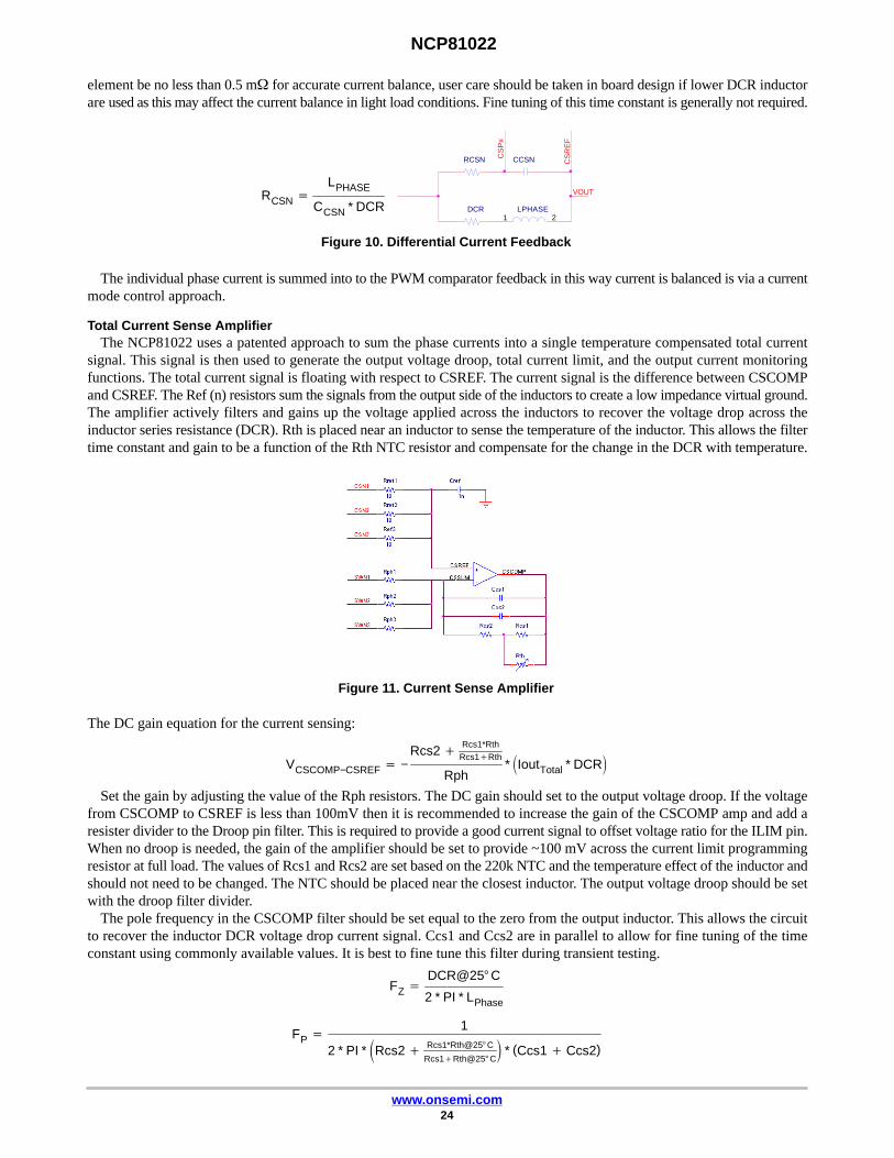
element be no less than 0.5 m� for accurate current balance, user care should be taken in board design if lower DCR inductorare used as this may affect the current balance in light load conditions. Fine tuning of this time constant is generally not required.
VOUT
21
CCSNRCSN
DCR LPHASE
CS
Px
CS
RE
F
RCSN �LPHASE
CCSN * DCR
Figure 10. Differential Current Feedback
The individual phase current is summed into to the PWM comparator feedback in this way current is balanced is via a currentmode control approach.
Total Current Sense AmplifierThe NCP81022 uses a patented approach to sum the phase currents into a single temperature compensated total current
signal. This signal is then used to generate the output voltage droop, total current limit, and the output current monitoringfunctions. The total current signal is floating with respect to CSREF. The current signal is the difference between CSCOMPand CSREF. The Ref (n) resistors sum the signals from the output side of the inductors to create a low impedance virtual ground.The amplifier actively filters and gains up the voltage applied across the inductors to recover the voltage drop across theinductor series resistance (DCR). Rth is placed near an inductor to sense the temperature of the inductor. This allows the filtertime constant and gain to be a function of the Rth NTC resistor and compensate for the change in the DCR with temperature.
Figure 11. Current Sense Amplifier
The DC gain equation for the current sensing:
VCSCOMP−CSREF � −Rcs2 �
Rcs1*RthRcs1�Rth
Rph* �IoutTotal * DCR�
Set the gain by adjusting the value of the Rph resistors. The DC gain should set to the output voltage droop. If the voltagefrom CSCOMP to CSREF is less than 100mV then it is recommended to increase the gain of the CSCOMP amp and add aresister divider to the Droop pin filter. This is required to provide a good current signal to offset voltage ratio for the ILIM pin.When no droop is needed, the gain of the amplifier should be set to provide ~100 mV across the current limit programmingresistor at full load. The values of Rcs1 and Rcs2 are set based on the 220k NTC and the temperature effect of the inductor andshould not need to be changed. The NTC should be placed near the closest inductor. The output voltage droop should be setwith the droop filter divider.
The pole frequency in the CSCOMP filter should be set equal to the zero from the output inductor. This allows the circuitto recover the inductor DCR voltage drop current signal. Ccs1 and Ccs2 are in parallel to allow for fine tuning of the timeconstant using commonly available values. It is best to fine tune this filter during transient testing.
FZ �DCR@25°C
2 * PI * LPhase
FP �1
2 * PI * �Rcs2 � Rcs1*Rth@25°C
Rcs1�Rth@25°C� * (Ccs1 � Ccs2)

NCP81022
www.onsemi.com25
Programming the Current LimitThe current−limit thresholds are programmed with a resistor between the ILIM and CSCOMP pins. The ILIM pin mirrors
the voltage at the CSREF pin and the current limit comparators. Set the value of the current limit through CSREF− CSCOMPvoltage at IoutLIMIT condition as shown below:
RILIM �
Rcs2�Rcs1*Rth
Rcs1�RthRph
* �IoutLIMIT * DCR�
10 �Aor RILIM �
VCSREF−CSCOMP@ILIMIT
10 �A
Programming DROOP and DAC feedforwardProgramming Rdroop sets the gain of the DAC feed−forward and Cdroop provides the time constant to cancel the time
constant of the system per the equations below. Cout_total is the total output capacitance of the system design.
CdroopRdroop
Rdroop = (Cout_total)*loadline*453.6*106
Cdroop = (loadline*(Cout_total))/Rdroop
Figure 12. Droop RC
Programming IOUTThe IOUT pin sources a current equal to the ILIM sink current gained by the IOUT Current Gain. The voltage on the IOUT
pin is monitored by the internal A/D converter and should be scaled with an external resistor to ground such that a load equalto ICCMAX generates a 2 V signal on IOUT. A pull−up resistor from 5 V VCC can be used to offset the IOUT signal positiveif needed.
RIOUT �2.0 V * RLIMIT
10 *Rcs2� Rcs1*Rth
Rcs1�RthRph
* �IoutICC_MAX * DCR�
Precision OscillatorA programmable precision oscillator is provided. The clock oscillator serves as the master clock to the ramp generator circuit.
This oscillator is programmed by a resistor to ground on the ROSC pin. The oscillator can also be programmed over the SMBusinterface through register 0xF7. The oscillator frequency range is between 200 kHz/phase to 1 MHz/phase in 32 steps. TheROSC pin provides approximately 2 V out and the source current is mirrored into the internal ramp oscillator.

NCP81022
www.onsemi.com26
Figure 13. NCP81022 Operating Frequency vs. Rosc
Figure 14. PWM vs. Register Code
The oscillator generates triangle ramps that are 0.5~2.5 V in amplitude depending on the VRMP pin voltage to provide inputvoltage feed forward compensation. The ramps are equally spaced out of phase with respect to each other and the signal phaserail is set half way between phases 1 and 2 of the multi phase rail for minimum input ripple current.
Programming the Ramp Feed−Forward CircuitThe ramp generator circuit provides the ramp used by the PWM comparators. The ramp generator provides voltage
feed−forward control by varying the ramp magnitude with respect to the VRMP pin voltage. The VRMP pin also has a 4 VUVLO function. The VRMP UVLO is only active after the controller is enabled. The VRMP pin is a high impedance inputwhen the controller is disabled.The PWM ramp time is changed according to the following,
VRAMPpk�pkPP � 0.1 * VVRMP

NCP81022
www.onsemi.com27
Vin
Comp−IL
Duty
Vramp_pp
Figure 15. Ramp Feedforward
Programming TRBST#The TRBST# pin provides a signal to offset the output after load release overshoot. This network should be fine tuned during
the board tuning process and is only necessary in systems with significant load release overshoot. The TRBST# network allowsmaximum boost for low frequency load release events to minimize load release ringing back undershoot. The network timeconstants are set up to provide a TRBST# roll of at higher frequencies where it is not needed. Cboost1*Rbst1 controls the timeconstant of the load release boost. This should be set to counter the under shoot after load release. Rbst1+ Rbst2 controls themaximum amount of boost during rapid step loading. Rbst2 is generally much larger then Rbst1. The Cboost2*Rbst2 timeconstant controls the roll off frequency of the TRBST# function.
Rbst2
Cboost1
Rbst1
Cboost2 Rbst3
FB TRBST
Figure 16. TRBST Circuit
PWM ComparatorsDuring steady state operation, the duty cycle is centered on the valley of the triangle ramp waveform and both edges of the
PWM signal are modulated. During a transient event the duty will increase rapidly and proportionally turning on all phasesas the error amp signal increases with respect to the ramps to provide a highly linear and proportional response to the step load.
Phase Detection Sequence for Main RailDuring start−up, the number of operational phases and their phase relationship is determined by the internal circuitry
monitoring the CSN Pins. Normally, NCP81022 main rail operates as a 4−phase PWM controller. Connecting CSN4 pin toVCC programs 3−phase operation, connecting CSN2 and CSN4 pin to VCC programs 2−phase operation, connecting CSN2,CSN3 and CSN4 pin to VCC programs 1−phase operation. Prior to soft start, while ENABLE is high, CSN4 to CSN2 pins sinkapproximately 50 �A. An internal comparator checks the voltage of each pin versus a threshold of 4.5V. If the pin is tied toVCC, its voltage is above the threshold. Otherwise, an internal current sink pulls the pin to GND, which is below the threshold.PWM1 is low during the phase detection interval, which takes 30us. After this time, if the remaining CSN outputs are not pulledto VCC, the 50 �A current sink is removed, and NCP81022 main rail functions as normal 4 phase controller. If the CSNsare pulled to VCC, the 50 �A current source is removed, and the outputs are driven into a high impedance state.
The PWM outputs are logic−level devices intended for driving fast response external gate drivers such as the NCP5901 andNCP5911. Because each phase is monitored independently, operation approaching 100% duty cycle is possible. In addition,more than one PWM output can be on at the same time to allow overlapping phases.
PHASE DETECTION
Number ofphases
Programming pin CSNX Unused pins
4+1 All CSN pin connected normally. No unused pins
3+1 Connect CSN4 to VCC through a 2k resistor.All other CSN pins connected normally.
Float PWM4Ground CSP4

NCP81022
www.onsemi.com28
PHASE DETECTION
Number ofphases
Unused pinsProgramming pin CSNX
2+1 Connect CSN2 and CSN4 to VCC through a 2k resistor.All other CSN pins connected normally.
Float PWM4 and PWM2Ground CSP4, and CSP2
1+1 Connect CSN2, CSN3 and CSN4 to VCC through a 2k res-istor.All other CSN pins connected normally.
Float PWM4, PWM3 and PWM2Ground CSP4, CSP3 and CSP2
4+0 CSN1NB pulled to VCC through 2k resistor.
All other CSN pins connected normally.
Float PWM1NB,Ilim NB, Diffout NB, Comp NB, TRB-STNB and CScompNBGround IoutNB, DroopNB, FBNB, CSSUM-NB,CSPNB and VDDNB
3+0 Connect CSN4 and CSN1NB to VCC through a 2k resistor.
All other CSN pins connected normally.
Float PWM4 PWM1NB,Ilim NB, Diffout NB, CompNB, TRBSTNB and CScompNBGround CSP4, IoutNB, DroopNB, FBNB, CSSUM-NB,CSPNB and VDDNB
2+0 Connect CSN2, CSN4 and CSN1NB to VCC through a 2kresistor.All other CSN pins connected normally.
Float PWM4, PWM2, PWM1NB,Ilim NB, Diffout NB,Comp NB, TRBSTNB and CScompNBGround CSP4, CSP2 IoutNB, DroopNB, FBNB,CSSUMNB,CSPNB and VDDNB
1+0 Connect CSN2, CSN3, CSN4 and CSN1NB to VCC througha 2k resistor.CSN1 pin connected normally.
Float PWM4, PWM3, PWM2, PWM1NB,Ilim NB,Diffout NB, Comp NB, TRBSTNB and CScompNBGround CSP4, CSP3, CSP2 IoutNB, DroopNB, FB-NB, CSSUMNB,CSPNB and VDDNB
Protection FeaturesOutput voltage out of regulation is defined as either a UVP or OVP event. The protection mechanism in case of either type
of fault is described in this section.
Gate Driver UVLO ProtectionThe NCP811022 monitors Vcc and DRON signals during UVLO restart, as shown in Figure 17.
DAC
Gate Driver Pulls DRONLow during driver UVLO
and Calibration
If DRON is pulled low thecontroller will hold off its
startup
Figure 17. Gate Driver UVLO Restart
VCC
UVLO
DRON
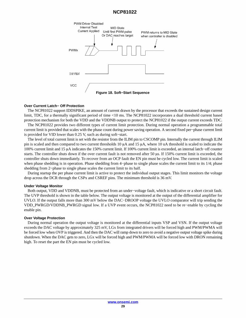
Soft StartSoft start is implemented internally. A digital counter steps the DAC up from zero to the target voltage based on the
predetermined slew rate programmed on startup. The controller enables and sets the PWM signal to the 2.0 V MID state toindicate that the drivers should be in diode mode. The COMP pin released to begin soft−start. The DAC will ramp from Zeroto the target DAC codes and the PWM outputs will begin to fire. Each phase will move out of the MID state when the first PWMpulse is produced preventing the discharge of a pre−charged output.
NCP81022
www.onsemi.com29
Figure 18. Soft−Start Sequence
Over Current Latch− Off ProtectionThe NCP81022 support IDDSPIKE, an amount of current drawn by the processor that exceeds the sustained design current
limit, TDC, for a thermally significant period of time <10 ms. The NCP81022 incorporates a dual threshold current basedprotection mechanism for both the VDD and the VDDNB output to protect the NCP81022 if the output current exceeds TDC.
The NCP81022 provides two different types of current limit protection. During normal operation a programmable totalcurrent limit is provided that scales with the phase count during power saving operation. A second fixed per−phase current limitis provided for VID lower than 0.25 V, such as during soft−start.
The level of total current limit is set with the resistor from the ILIM pin to CSCOMP pin. Internally the current through ILIMpin is scaled and then compared to two current thresholds 10 �A and 15 �A, where 10 uA threshold is scaled to indicate the100% current limit and 15 �A indicates the 150% current limit. If 100% current limit is exceeded, an internal latch−off counterstarts. The controller shuts down if the over current fault is not removed after 50 �s. If 150% current limit is exceeded, thecontroller shuts down immediately. To recover from an OCP fault the EN pin must be cycled low. The current limit is scaledwhen phase shedding is in operation. Phase shedding from 4−phase to single phase scales the current limit to its 1/4; phaseshedding from 2−phase to single phase scales the current limit to its half.
During startup the per phase current limit is active to protect the individual output stages. This limit monitors the voltagedrop across the DCR through the CSPx and CSREF pins. The minimum threshold is 36 mV.
Under Voltage MonitorBoth output, VDD and VDDNB, must be protected from an under−voltage fault, which is indicative or a short circuit fault.
The UVP threshold is shown in the table below. The output voltage is monitored at the output of the differential amplifier forUVLO. If the output falls more than 300 mV below the DAC−DROOP voltage the UVLO comparator will trip sending theVDD_PWRGD/VDDNB_PWRGD signal low. If a UVP event occurs, the NCP81022 need to be re−enable by cycling theenable pin.
Over Voltage ProtectionDuring normal operation the output voltage is monitored at the differential inputs VSP and VSN. If the output voltage
exceeds the DAC voltage by approximately 325 mV, LGx from integrated drivers will be forced high and PWM/PWMA willbe forced low when OVP is triggered. And then the DAC will ramp down to zero to avoid a negative output voltage spike duringshutdown. When the DAC gets to zero, LGx will be forced high and PWM/PWMA will be forced low with DRON remaininghigh. To reset the part the EN pin must be cycled low.

NCP81022
www.onsemi.com30
DACVSP_VSN
OVP Threshold
Latch Off
OVPTriggered
PWM
Figure 19. OVP Threshold Behavior
Parameter Min Typ Max Description
UVP Threshold 300 mV 325 mV 350 mV Voltage below programmed VID
OVP Threshold 300 mV 325 mV 350 mV Voltage below programmed VID
Non−Fault domainPower down or PWRGDDelay
1 10 �S
Layout NotesThe NCP81022 has differential voltage and current monitoring. This improves signal integrity and reduces noise issues
related to layout for easy design use. To insure proper function there are some general rules to follow:Careful layout in per phase and total current sensing are critical for jitter minimization, accurate current balancing and ILIM
monitoring. Give the first priority in component placement and trace routing to per phase and total current sensing circuit. Theper phase inductor current sense RC filters should always be placed as close to the CSREF and CSP pins on the controller aspossible. The filter cap from CSCOMP to CSREF should also be close to the controller. The temperature−compensate resistorRTH should be placed as close as possible to the Phase 1 inductor. The wiring path between RCSx and RPHx should be kept asshort as possible and well away from switch node lines. The Refx resistors (10 �) connected to CSREF pin should be placednear the inductors to reduce the length of traces. The above layout notes are shown in the following diagram:
CSCOMP
CSSUM
CSREF+
−
CCS1
RCS1
RCS2
RTHPlace as close as possible
to nearest inductor
RPH1
RPH2
To Switch Nodes
Keep this path as short aspossible and well awayfrom switch node lines
CCS2
+
−
+
−
CSP1
CSP2
RREF1
RREF2
To VSense
OUT
RCSN1
RCSN2
CCSN1
CCSN2
ToSwitchNodes
Per phase current senseRC should be placedclose to CSPx pins
REFx resistors couldbe placed near theinductors to reducethe number of long
traces
Figure 20.

NCP81022
www.onsemi.com31
Place the VCC decoupling caps as close as possible to the controller VCC pin. For any RC filter on the VCC and VDDBPpins, the resistor should be no higher than 2.2 � to prevent large voltage drop.
The small high feed back cap from COMP to FB should be as close to the controller as possible. Keep the FB traces shortto minimize their capacitance to ground.
Digital InterfaceControl of the NCP81022 is carried out using the Digital Interface.The NCP81022 is connected to this bus as a slave device, under the control of a master controller.Data is sent over the serial bus in sequences of nine clock pulses: eight bits of data followed by an acknowledge bit from
the slave device. Transitions on the data line must occur during the low period of the clock signal and remain stable during thehigh period, because a low−to−high transition when the clock is high might be interpreted as a stop signal. The number of databytes that can be transmitted over the serial bus in a single read or write operation is limited only by what the master and slavedevices can handle.
1. When all data bytes have been read or written, stop conditions are established. In write mode, the master pulls thedata line high during the tenth clock pulse to assert a stop condition. In read mode, the master device overrides theacknowledge bit by pulling the data line high during the low period before the ninth clock pulse; this is known as NoAcknowledge. The master takes the data line low during the low period before the tenth clock pulse, and then highduring the tenth clock pulse to assert a stop condition.Any number of bytes of data can be transferred over the serial bus in one operation, but it is not possible to mix readand write in one operation because the type of operation is determined at the beginning and cannot subsequently bechanged without starting a new operation.
In the NCP81022, write operations contain one, two or three bytes, and read operations contain one or two bytes. Thecommand code or register address determines the number of bytes to be read or written, See the register map for moreinformation.
To write data to one of the device data registers or read data from it, the address pointer register must be set so thatthe correct data register is addressed (i.e. command code), and then data can be written to that register or read from it.
The first byte of a read or write operation always contains an address that is stored in the address pointer register. Ifdata is to be written to the device, the write operation contains a second data byte that is written to the registerselected by the address pointer register.
This write byte operation is shown in Figure 22. The device address is sent over the bus, and then R/W is set to 0.This is followed by two data bytes. The first data byte is the address of the internal data register to be written to,which is stored in the address pointer register. The second data byte is the data to be written to the internal dataregister.
2. The read byte operation is shown in Figure 23. First the command code needs to be written to the NCP81022 so thatthe required data is sent back. This is done by performing a write to the NCP81022 as before, but only the data bytecontaining the register address is sent, because no data is written to the register. A repeated start is then issued and aread operation is then performed consisting of the serial bus address; R/W bit set to 1, followed by the data byte readfrom the data register.
3. It is not possible to read or write a data byte from a data register without first writing to the address pointer register,even if the address pointer register is already at the correct value.
4. In addition to supporting the send byte, the NCP81022 also supports the read byte, write byte, read word and writeword protocols.
1 9 1 9
0 0 01 1 ADDRESS R/W D7 D6 D5 D4 D3 D2 D1 D0
SCL
SDA
START BYMASTER
ACK. BYNCP81022
FRAME 1SERIAL BUS ADDRESS BYTE
FRAME 2COMMANDCODE
ACK. BYNCP81022
STOP BYMASTER
Figure 21. Send Byte

NCP81022
www.onsemi.com32
1 9 1 9
0 0 01 1 ADDRESS R/W D7 D6 D5 D4 D3 D2 D1 D0
SCL
SDA
START BYMASTER
ACK. BYNCP81022
FRAME 1SERIAL BUS ADDRESS BYTE
FRAME 2COMMANDCODE
FRAME 3DATA BYTE
SCL (CONTINUED)
SDA (CONTINUED)
ACK. BYNCP81022
ACK. BYNCP81022
STOP BYMASTER
91
D7 D6 D5 D4 D3 D2 D1 D0
Figure 22. Write Byte
Figure 23. Read Byte
The following abbreviations are used in the diagrams:S − STARTP − STOPR − READW − WRITEA − ACKNOWLEDGEA− NO ACKNOWLEDGEThe NCP81022 uses the following write protocols.
Send ByteIn this operation, the master device sends a single command byte to a slave device as follows:
1. The master device asserts a start condition on SDA.2. The master sends the 7−bit slave address followed by the write bit (low).3. The addressed slave device asserts ACK on SDA.4. The master sends a command code.5. The slave asserts ACK on SDA.6. The master asserts a stop condition on SDA and the transaction ends.
For the NCP81022, the send byte protocol is used to clear Faults. This operation is shown in Figure 22.

NCP81022
www.onsemi.com33
SLAVEADDRESS
COMMANDCODE AAWS P
2 4 6531
If the master is required to read data from the register immediately after setting up the address, it can assert a repeat startcondition immediately after the final ACK and carry out a single byte read without asserting an intermediate stop condition.
Write ByteIn this operation, the master device sends a command byte and one data byte to the slave device as follows:
1. The master device asserts a start condition on SDA.2. The master sends the 7−bit slave address followed by the write bit (low).3. The addressed slave device asserts ACK on SDA.4. The master sends a command code.5. The slave asserts ACK on SDA.6. The master sends a data byte.7. The slave asserts ACK on SDA.8. The master asserts a stop condition on SDA and the transaction ends.
The byte write operation is shown in Figure 22.
SLAVEADDRESS
COMMANDCODE
DATAAAWS A P
2 4 6531 7 8
Write WordIn this operation, the master device sends a command byte and two data bytes to the slave device as follows:
1. The master device asserts a start condition on SDA.2. The master sends the 7−bit slave address followed by the write bit (low).3. The addressed slave device asserts ACK on SDA.4. The master sends a command code.5. The slave asserts ACK on SDA.6. The master sends the first data byte.7. The slave asserts ACK on SDA.8. The master sends the second data byte.9. The slave asserts ACK on SDA.
10. The master asserts a stop condition on SDA and the transaction ends.
SLAVEADDRESS
COMMANDCODE
DATA(LSB)
AAWS A P
2 4 6531 7 8
DATA(MSB)
A
109
Block WriteIn this operation, the master device sends a command byte and a byte count followed by the stated number of data bytes to
the slave device as follows:1. The master device asserts a START condition on SDA.2. The master sends the 7−bit slave address followed by the write bit (low).3. The addressed slave device asserts ACK on SDA.4. The master sends a command code5. The slave asserts ACK on SDA6. The master sends the byte count N7. The slave asserts ACK on SDA8. The master sends the first data byte9. The slave asserts ACK on SDA
10. The master sends the second data byte.11. The slave asserts ACK on SDA12. The master sends the remainder of the data byes
NCP81022
www.onsemi.com34
13. The slave asserts an ACK on SDA after each data byte.14. After the last data byte the master asserts a STOP condition on SDA
SLAVEADDRESS
COMMANDCODE
DATABYTE 1
AAWS
2 4 6531 7 8 9
BYTE COUNT= N
A A
...10
DATABYTE 2
A ... DATABYTE N
PA
11 12 13 14
Extended Write CommandAn extended write command is executed with the following format:
1. The master device asserts a START condition on SDA2. The master sends the 7−bit slave address followed by the write bit (low).3. The addressed slave device asserts ACK on SDA4. The master sends a command extension code (FEh)5. The slave asserted ACK on SDA6. The master sends a command code7. The slave asserted ACK on SDA8. The master sends a data byte.9. The slave asserts ACK on SDA.
10. The master asserts a stop condition on SDA and the transaction ends.
S Slave Address W ACommandExtension Code A
CommandCode A
1 2 3 4 65 7
Data Byte A P
8 9 10
The NCP81022 uses the following SMBus read protocols.
Read ByteIn this operation, the master device receives a single byte from a slave device as follows:
1. The master device asserts a start condition on SDA.2. The master sends the 7−bit slave address followed by the write bit (low).3. The addressed slave device asserts ACK on SDA.4. The master sends a command code.5. The slave asserted ACK on SDA.6. The master sends a repeated start condition on SDA7. The master sends the 7 bit slave address followed by the read bit (high)8. The slave asserts ACK on SDA9. The slave sends the Data Byte
10. The master asserts NO ACK on SDA.11. The master asserts a stop condition on SDA and the transaction ends.
SLAVEADDRESS
COMMANDCODE
DATAAAWS A P
2 4 6531 7 8
SSLAVE
ADDRESSAR
109 11
Read WordIn this operation, the master device receives two data bytes from a slave device as follows:
1. The master device asserts a start condition on SDA.2. The master sends the 7−bit slave address followed by the write bit (low).

NCP81022
www.onsemi.com35
3. The addressed slave device asserts ACK on SDA.4. The master sends a command code.5. The slave asserted ACK on SDA.6. The master sends a repeated start condition on SDA7. The master sends the 7 bit slave address followed by the read bit (high)8. The slave asserts ACK on SDA9. The slave sends the first Data Byte (low Data Byte)
10. The master asserts ACK on SDA.11. The slave sends the second Data Byte (high Data Byte)12. The masters asserts a No ACK on SDA13. The master asserts a stop condition on SDA and the transaction ends
SLAVEADDRESS
COMMANDCODE
DATA(LSB)
AAWS A
2 4 6531 7 8
SSLAVE
ADDRESSAR
109
DATA(MSB)
A P
1211 13
Block ReadIn this operation, the master device sends a command byte, the slave sends a byte count followed by the stated number of
data bytes to the master device as follows:1. The master device asserts a START condition on SDA.2. The master sends the 7−bit slave address followed by the write bit (low).3. The addressed slave device asserts ACK on SDA.4. The master sends a REPEATED START condition on SDA5. The master sends the 7−bit slave address followed by the read bit (high).6. The slave asserts ACK on SDA7. The slave sends the byte count N8. The master asserts ACK on SDA9. The slave sends the first data byte
10. The master asserts ACK on SDA11. The slave sends the remainder of the data byes, the master asserts an ACK on SDA after each data byte.12. After the last data byte the master asserts a No ACK on SDA.13. The master asserts a STOP condition on SDA
SLAVEADDRESS
BYTE COUNT= N
AWS
2 4 6531 7
S SLAVEADDRESS
AR
8 1211
DATABYTE N
A P
13
ADATA
BYTE 1A ...109
Extended Read CommandAn extended Read byte command is executed with the following format and is shown in figure TBD below:
1. The master device asserts a START condition on SDA.2. The master sends the 7−bit slave address followed by the write bit (low).3. The addressed slave device asserts ACK on SDA4. The master sends a command extension code (FEh)5. The slave asserted ACK on SDA.6. The master sends a command code7. The slave asserted ACK on SDA.8. The master sends a REPEATED START condition on SDA9. The master sends the 7 bit slave address followed by the read bit (high)

NCP81022
www.onsemi.com36
10. The slave asserts ACK on SDA11. The slave sends the Data Byte
12. The master asserts NO ACK on SDA.13. The master asserts a stop condition on SDA and the transaction ends.
S S lave Address W AComm andExtension Code A
Comm andCode
A
1 2 3 4 65 7
S S lave Address R A Data Byte A P
8 9 10 11 12 13
The NCP81022 includes a timeout feature. If there is no Bus activity for 35 ms, the NCP81022 assumes that the bus is lockedand releases the bus. This prevents the device from locking or holding the SMBus expecting data. Some SMBus controllerscannot handle the SMBus timeout feature, so it can be disabled.
To prevent rogue programs or viruses from accessing critical NCP81022 register settings, the lock bit can be set. Setting Bit 0of the Lock/Reset sets the lock bit and locks critical registers. In this mode, certain registers can no longer be written to untilthe NCP81022 is powered down and powered up again. For more information on which registers are locked see the registermap.
REGISTER MAP
CMDCode R/W Default Description #Bytes Comment
0x01 R/W 0x80 Operation 1 00xx xxxx – Immediate Off01xx xxxx – Soft Off1000 xxxx – On (slew rate set by soft start) – Default1001 10xx – Margin Low (Act on Fault)1010 10xx – Margin High (Act on Fault)
0x02 R/W 0x17 ON_OFF_Config 1 Configures how the controller is turned on and off
Bit Default Comment
7:6 00 Reserved for Future Use
5 1 Reserved
4 1 This bit is read only. Switching starts whencommanded by the Control Pin and the OperationCommand, as set in Bits 3:0
3 0 0 : Unit ignores OPERATION commands over theInterface1: Unit responds to OPERATION command,power up may also depend upon Control input, asdescribed in Bit 2
2 1 0: Unit ignores Main Rail EN pin1: Unit responds Main Rail EN pin, power up mayalso depend upon the Operation Register, asdescribed for Bit 3
1 1 Control Pin polarity0 = Active Low1 = Active High
0 1 This bit is read only. 1 means that when thecontroller is disabled it will either immediately turnoff or soft off (as set in the Operation Command)
0x03 W NA Clear_Faults 0 Writing any value to this command code will clear all Status Bits immediately.
0x10 R/W 0x00 Write_Protect 1 The Write_protect command is used to control writing to the device. There is also a lock bit in theManufacturer Specification Registers that once set will disable writes to all commands until thepower to the NCP81022 is cycled.
0x19 R 0xB0 Capability 1 This command allows the host to get some information on the SMBus device
Bit Default Comment
7 1 PEC (Packet Error Checking is supported)
6:5 01 Max supported bus speed is 400kHz
4 0 Reverved
3:0 000 Reserved for future use
0x20 R 0x22 Vout_Mode 1 The NCP81022 supports SVI2 VID mode for programming the output voltage

NCP81022
www.onsemi.com37
REGISTER MAP
CMDCode Comment#BytesDescriptionDefaultR/W
0x21 R/W 0x00 Vout_Command 2 Sets the output voltage using the SVI2 VID table decoding
0x24 R/W 0x00 Vout_Max 2 Sets the max output voltage when programming VID Code through SMBus. When programmingVID through SVI2, then SVI2 Vout max applies.
0x25 R/W 0x0018 VOUT_ MARGIN_HIGH
2 Sets the output voltage when operation command is set to Margin High. Programmed in VID Mode.
0x26 R/W 0x00A8 VOUT_ MARGIN_LOW
2 Sets the output voltage when operation command is set to Margin Low. Programmed in VID Mode.
0x38 R/W 0x0001 IOUT_CAL_ GAIN 2 Sets the ratio of voltage sensed to current output. Scale is Linear and is expressed in 1/�
0x39 R/W 0x0000 Iout Offset
0x4A R/W Iout _Fault_limit This sets the output current fault limit. Once exceeded Bit 7 of the Status IOUT Command gets setand the FAULT output gets asserted (if not masked)
0x55 R/W 0x0010 VIN_OV_ FAULT LIMIT 2 This sets the input over voltage fault limit. Once exceeded the VIN Overvoltage Fault Bit, Bit 7, getsset in the Status Input Register and the FAULT output is asserted. This limit is set using LinearMode, in V.
0x68 R/W 0x012C POUT_OP_ FAULTLIMIT
2 This sets the output power over power fault limit. Once exceeded Bit 1 of the Status IOUTCommand gets set and the FAULT output gets asserted (if not masked)
0x78 R 0x00 STATUS BYTE 1 Bit Name Description
7 BUSY A fault was declared because the NCP81022 wasbusy and unable to respond
6 OFF This bit is set whenever the NCP81022 is notswitching
5 VOUT_OV This bit gets set whenever the NCP81022 goesinto OVP mode.
4 IOUT_OC This bit gets set whenever the NCP81022 latchesoff due to an over current event.
3 Reserved Reserved
2 Reserved Reserved
1 Reserved Reserved
0 None of the Above A fault has occurred which is not one of the above
0x79 R 0x0000 STATUS WORD 2 Byte Bit Name Description
Low 7 Res Reserved for future use
Low 6 OFF This bit is set whenever the NCP81022 is notswitching
Low 5 VOUT_OV This bit gets set whenever the NCP81022 goesinto OVP mode
Low 4 IOUT_OC This bit gets set whenever the NCP81022 latchesoff due to an over current event
Low 3 Reserved Reserved
Low 2 Reserved Reserved
Low 1 Reserved Reserved
Low 0 None of the Above A fault has occurred which is not one of the above
Byte Bit Name Description
High 7 VOUT This bit gets set whenever the measured outputvoltage goes outside its power good limits or anOVP event has taken place, i.e. any bit in StatusVOUT is set
High 6 Iout/Pout This bit gets set whenever the measured outputcurrent or power exceeds its warning limit or goesinto OCP. i.e. any bit in Status IOUT is set
High 5 Input This bit gets set whenever the measured inputvoltage falls outside its Fault limit
High 4 MFR A manufacturer specific warning or fault hasoccurred
High 3 VDD_PWRGD The VDD_PWRGD signal is deasserted. Same asPowerGood in General Status
High 2 Reserved Reserved
High 1 OTHER A Status bit in Status Other is asserted
High 0 Res Reserved for future use

NCP81022
www.onsemi.com38
REGISTER MAP
CMDCode Comment#BytesDescriptionDefaultR/W
0x7A R 0x00 STATUS VOUT 1 Bit Name Description
7 VOUT_OVERVOLTAGE FAULT
This bit gets set whenever an OVP Event takesplace
6 VOUT_OVERVOLTAGE WARNING
Not Supported
5 VOUT_ UNDERVOLTAGEWARNING
Not supported
4 Reserved Reserved
3 VOUT_MAXWarning
Not supported, Can’t program an output greaterthan max VID as there are no bits to program it
2 Reserved Reserved
1 Reserved Reserved
0 Reserved Reserved
0x7B R 0x00 STATUS IOUT 1 Bit Name Description
7 IOUT OvercurrentFault
This bit gets set if the NCP81022 latches off dueto an OCP Event
6 Reserved Reserved for future use
5 IOUT OvercurrentWarning
Not supported
4 Reserved Reserved for future use
3 Reserved Reserved for future use
2 Reserved Reserved for future use
1 POUT Over PowerFault
This bit gets set if the measured POUT exceedsthe FAULT Limit
0 Reserved Reserved
0x7C R 0x00 STATUS INPUT 1 Bit Name Description
7 VIN OvervoltageFAULT
This bit gets set when the input voltage goesabove its programmed FAULT limit
6 Reserved Reserved for future use.
5 Reserved Reserved for future use.
4 Reserved Reserved for future use.
3 Reserved Reserved for future use.
2 Reserved Reserved for future use.
1 Reserved Reserved for future use.
0 Reserved Reserved for future use.
0x88 R 0x00 Read_VIN 2 Readback of input voltage, measured using VRMP Input. Readback is in linear mode
0x8B R 0x00 Read_VOUT 2 Readback output voltage. Voltage is read back in VID Mode
0x8C R 0x00 Read_IOUT 2 Readback output current. Current is read back in Linear Mode (Amps)
0x96 R 0x00 Read_POUT 2 Readback Output Power, read back in Linear Mode in W’s.
0x99 R 0x1A MFR_ID 2 0x1A
0x9A R 0x1022 MFR_ MODEL 2 0x1022
0x9B R 0x00 MFR_ REVISION 1 0x00
0xD0 R/W 0x00 Lock/Reset 1 Bit 0 = Lock Bit Bit 1 = Reset Bit
0xD1 R/W 0x01 Manufacturer Config 1 Bit 0 = ADCBit 1 = ReservedBit 2 = ReservedBit 3 = SMB_TO_EN

NCP81022
www.onsemi.com39
REGISTER MAP
CMDCode Comment#BytesDescriptionDefaultR/W
0xD2 R/W 0x00 VR Config 1 1 Bit 0= 0, All SVI2 parameters programmed through SVI2; Default = 01, All SVI2 parameters programmed through Digital interfaceBit 1 = ReservedBit 2 = Voltage rail; Voltage rail = 0 then main rail is programmable, Voltage rail = 1 then North Bridge rail is programmable over SMBus.Default = 0Bit 3 = ReservedBit 4 = ReservedBit 5 = ReservedBit 6 = CLIM_EN, 0 = CLIM Latch off enabled = default, 1 = CLIM Latchoff disabledBit 7 = Reserved
0xD3 R/W 0x03 VR Config 2 1
Bit Name
Comment
PSI0# PSI1# Phase
0:1 PSI0/PSI1 0 0 1−Phase DCM
0 1 1−Phase CCM
1 0 Full Phase
1 1 Full Phase
2 NotSupported
3:4 Reserved
5 NotSupported
6 Reserved
0xD4 R Vout_Linear 2 Readback of output voltage in Linear Mode. Exponent fixed at −9
0xD5 R/W 0x02 Vout Trim 1 Programmable Offset Voltage. Data format is 2’s complement00 = 001−25 mV10 = initial programmed offset (default)11 = +25 mV11
0xD7 R/W 0x00 Initial offset
0xE3 R/W 0x08 Current Limit 1 Sets the value of the current limit relative to the current limit set by the ILIM pin.
0xE4 R/W 0x03 Loadline 1 This register sets the internal loadline attenuation. The max loadline is controlled externally bysetting the gain of the CSA. The max loadline can be adjusted between 0% and 100% of theexternal loadline.000−Remove all loadline drop from output001−LL slope 12.9%010−LL slope 25.8%011−LL slope 38.7%100− LL slope 51.6%101− LL slope 64.8%110 LL slope 77.4%111 LL slope 90.3%
0xE5 R/W 0x03 Initial loadline
0xE6 R/W 0x00 Special purpose offset
0xE7 R 0X00 Current VID 2 This register reports back the current VID Code being output incl. Offset being output
0xF3 R 0x00 Vboot 1 Read back Vboot value− VID code format
0xF7 R/W 0x0A OSC Freq. 1 This register adjusts the oscillator frequency from 240Khz to 1 MHz
0xFB R/W 0x00 General Status Bit 0 – ReadyBit 1 – VDD_PWRGDBit 3 – RESERVEDBit 4 – RESERVED Bit 5 − Clim limit exceeded but not long enough for Latch off
0xFC R 0x00 Reserved Reserved
0xFD R 0x00 Phase Status Bit 0 = Phase 1Bit 1 = Phase 2Bit 2 = Phase 3Bit 3 = Phase 4

NCP81022
www.onsemi.com40
ORDERING INFORMATION
Device Package Shipping†
NCP81022MNTXG QFN52(Pb−Free)
2500 / Tape & Reel
†For information on tape and reel specifications, including part orientation and tape sizes, please refer to our Tape and Reel PackagingSpecifications Brochure, BRD8011/D.
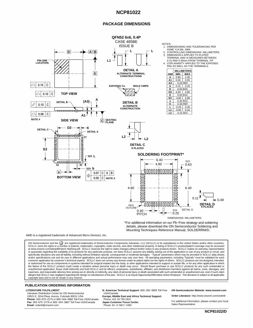
NCP81022
www.onsemi.com41
PACKAGE DIMENSIONS
QFN52 6x6, 0.4PCASE 485BE
ISSUE B
SEATINGNOTE 4
K
0.10 C
(A3) A
A1
D2
b
1
14
27
52
E2
52X
L
BOTTOM VIEW
DETAIL C
TOP VIEW
SIDE VIEW
D A B
E
0.10 C
ÉÉÉÉÉÉÉÉÉ
PIN ONELOCATION
0.10 C
0.08 C
C
40
e A0.07 BC
0.05 C
NOTES:1. DIMENSIONING AND TOLERANCING PER
ASME Y14.5M, 1994.2. CONTROLLING DIMENSIONS: MILLIMETERS.3. DIMENSION b APPLIES TO PLATED
TERMINAL AND IS MEASURED BETWEEN0.15 AND 0.30mm FROM TERMINAL TIP
4. COPLANARITY APPLIES TO THE EXPOSEDPAD AS WELL AS THE TERMINALS.
DIM MIN MAXMILLIMETERS
A 0.80 1.00A1 0.00 0.05A3 0.20 REFb 0.15 0.25D 6.00 BSCD2 4.60 4.80E 6.00 BSC
4.80E2 4.60e 0.40 BSC
L 0.25 0.45L1 0.00 0.15
NOTE 3
PLANE
DIMENSIONS: MILLIMETERS
0.25
4.80
0.40
4.80
52X
0.6352X
6.40
6.40
*For additional information on our Pb−Free strategy and solderingdetails, please download the ON Semiconductor Soldering andMounting Techniques Reference Manual, SOLDERRM/D.
SOLDERING FOOTPRINT*
DETAIL B
L1
DETAIL A
L
ALTERNATE TERMINALCONSTRUCTIONS
L
ÉÉÉÉÉÉÉÉÉDETAIL B
MOLD CMPDEXPOSED Cu
ALTERNATECONSTRUCTION
K 0.30 REF
PITCH
52X
PKGOUTLINE
L2 0.15 REF
L2
DETAIL C8 PLACES
L2
DETAIL A
DETAIL D8 PLACES
0.11 0.49
DETAIL D
ON Semiconductor and the are registered trademarks of Semiconductor Components Industries, LLC (SCILLC) or its subsidiaries in the United States and/or other countries.SCILLC owns the rights to a number of patents, trademarks, copyrights, trade secrets, and other intellectual property. A listing of SCILLC’s product/patent coverage may be accessedat www.onsemi.com/site/pdf/Patent−Marking.pdf. SCILLC reserves the right to make changes without further notice to any products herein. SCILLC makes no warranty, representationor guarantee regarding the suitability of its products for any particular purpose, nor does SCILLC assume any liability arising out of the application or use of any product or circuit, andspecifically disclaims any and all liability, including without limitation special, consequential or incidental damages. “Typical” parameters which may be provided in SCILLC data sheetsand/or specifications can and do vary in different applications and actual performance may vary over time. All operating parameters, including “Typicals” must be validated for eachcustomer application by customer’s technical experts. SCILLC does not convey any license under its patent rights nor the rights of others. SCILLC products are not designed, intended,or authorized for use as components in systems intended for surgical implant into the body, or other applications intended to support or sustain life, or for any other application in whichthe failure of the SCILLC product could create a situation where personal injury or death may occur. Should Buyer purchase or use SCILLC products for any such unintended orunauthorized application, Buyer shall indemnify and hold SCILLC and its officers, employees, subsidiaries, affiliates, and distributors harmless against all claims, costs, damages, andexpenses, and reasonable attorney fees arising out of, directly or indirectly, any claim of personal injury or death associated with such unintended or unauthorized use, even if such claimalleges that SCILLC was negligent regarding the design or manufacture of the part. SCILLC is an Equal Opportunity/Affirmative Action Employer. This literature is subject to all applicablecopyright laws and is not for resale in any manner.
PUBLICATION ORDERING INFORMATIONN. American Technical Support: 800−282−9855 Toll FreeUSA/Canada
Europe, Middle East and Africa Technical Support:Phone: 421 33 790 2910
Japan Customer Focus CenterPhone: 81−3−5817−1050
NCP81022/D
AMD is a registered trademark of Advanced Micro Devices, Inc.
LITERATURE FULFILLMENT:Literature Distribution Center for ON Semiconductor19521 E. 32nd Pkwy, Aurora, Colorado 80011 USAPhone: 303−675−2175 or 800−344−3860 Toll Free USA/CanadaFax: 303−675−2176 or 800−344−3867 Toll Free USA/CanadaEmail: [email protected]
ON Semiconductor Website: www.onsemi.com
Order Literature: http://www.onsemi.com/orderlit
For additional information, please contact your localSales Representative