Embed Size (px)
Citation preview
© Semiconductor Components Industries, LLC, 2019
August, 2020 − Rev. 11 Publication Order Number:
NCD57080A/D
Isolated High Current IGBTGate Driver
NCD57080A, NCD57080B,NCD57080C
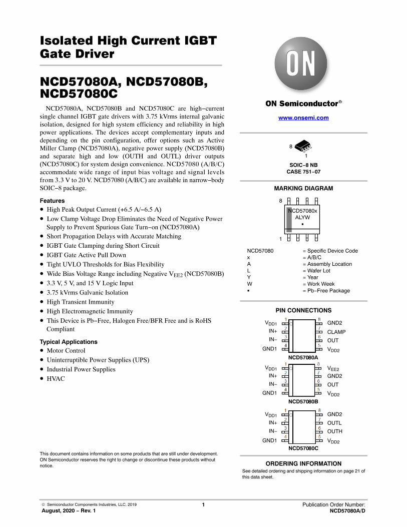
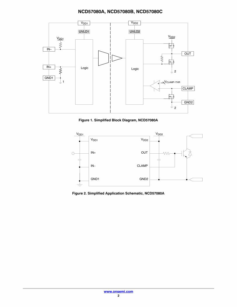
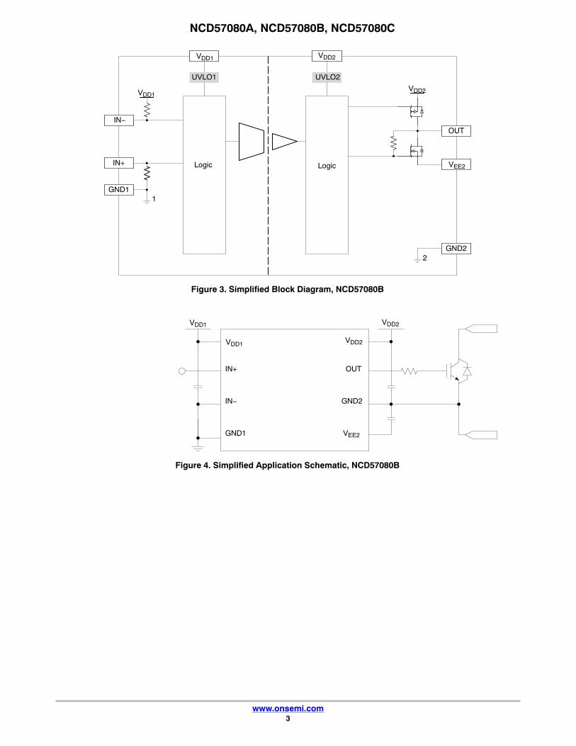
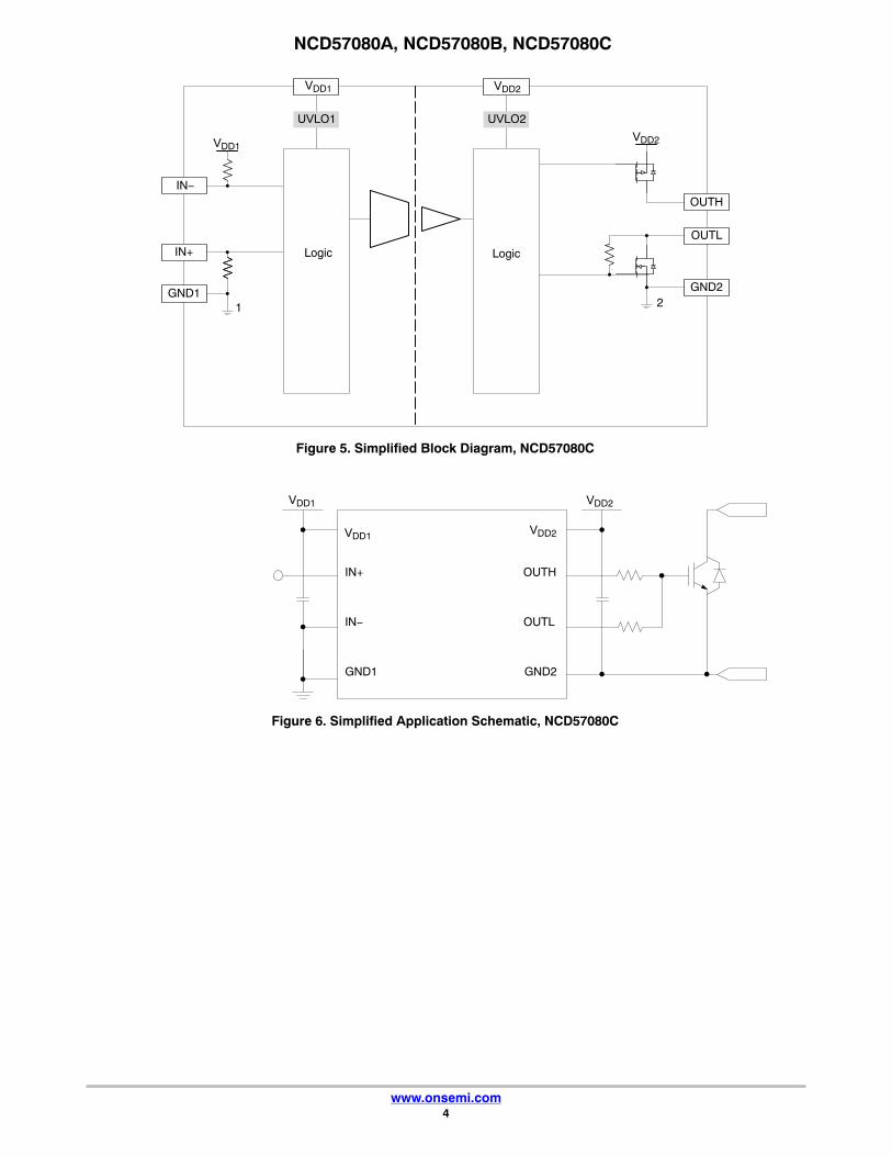
NCD57080A, NCD57080B and NCD57080C are high−currentsingle channel IGBT gate drivers with 3.75 kVrms internal galvanicisolation, designed for high system efficiency and reliability in highpower applications. The devices accept complementary inputs anddepending on the pin configuration, offer options such as ActiveMiller Clamp (NCD57080A), negative power supply (NCD57080B)and separate high and low (OUTH and OUTL) driver outputs(NCD57080C) for system design convenience. NCD57080 (A/B/C)accommodate wide range of input bias voltage and signal levelsfrom 3.3 V to 20 V. NCD57080 (A/B/C) are available in narrow−bodySOIC−8 package.
Features• High Peak Output Current (+6.5 A/−6.5 A)
• Low Clamp Voltage Drop Eliminates the Need of Negative PowerSupply to Prevent Spurious Gate Turn−on (NCD57080A)
• Short Propagation Delays with Accurate Matching
• IGBT Gate Clamping during Short Circuit
• IGBT Gate Active Pull Down
• Tight UVLO Thresholds for Bias Flexibility
• Wide Bias Voltage Range including Negative VEE2 (NCD57080B)
• 3.3 V, 5 V, and 15 V Logic Input
• 3.75 kVrms Galvanic Isolation
• High Transient Immunity
• High Electromagnetic Immunity
• This Device is Pb−Free, Halogen Free/BFR Free and is RoHSCompliant
Typical Applications• Motor Control
• Uninterruptible Power Supplies (UPS)
• Industrial Power Supplies
• HVAC
This document contains information on some products that are still under development.ON Semiconductor reserves the right to change or discontinue these products withoutnotice.
www.onsemi.com
See detailed ordering and shipping information on page 21 ofthis data sheet.
ORDERING INFORMATION
MARKING DIAGRAM
SOIC−8 NBCASE 751−07
PIN CONNECTIONS
NCD57080 = Specific Device Codex = A/B/CA = Assembly LocationL = Wafer LotY = YearW = Work Week� = Pb−Free Package
1
8
NCD57080xALYW
�
1
8
NCD57080A
NCD57080B
NCD57080C
VDD1
VDD1
VDD1
IN+
IN−
GND1
IN+
IN−
GND1
IN+
IN−
GND1
GND2
CLAMP
OUT
VDD2
VDD2
OUT
GND2
VEE2
GND2
OUTL
OUTH
VDD2
NCD57080A, NCD57080B, NCD57080C
www.onsemi.com2
Figure 1. Simplified Block Diagram, NCD57080A
IN−
GND1
CLAMP
IN+
UVLO2
+
−
VCLAMP−THR
UVLO1
VDD1
LogicLogic2
1
OUT
VDD2
GND2
VDD1 VDD2
2
Figure 2. Simplified Application Schematic, NCD57080A
CLAMP
GND2
OUTIN+
VDD1
GND1
IN−
VDD1 VDD2
VDD2
NCD57080A, NCD57080B, NCD57080C
www.onsemi.com3
Figure 3. Simplified Block Diagram, NCD57080B
IN−
GND1
IN+
UVLO2UVLO1
VDD1
LogicLogic
1
OUT
2
VDD2
GND2
VDD1 VDD2
VEE2
Figure 4. Simplified Application Schematic, NCD57080B
GND2
VEE2
OUTIN+
GND1
IN−
VDD1 VDD2
VDD1 VDD2
NCD57080A, NCD57080B, NCD57080C
www.onsemi.com4
Figure 5. Simplified Block Diagram, NCD57080C
IN−
GND1
IN+
GND2
UVLO2UVLO1
VDD1
LogicLogic
21
OUTH
OUTL
VDD2
VDD1 VDD2
Figure 6. Simplified Application Schematic, NCD57080C
OUTL
GND2
OUTHIN+
GND1
IN−
VDD1 VDD2
VDD1 VDD2
NCD57080A, NCD57080B, NCD57080C
www.onsemi.com5
Table 1. FUNCTION DESCRIPTION
Pin Name No. I/O Description
VDD1 1 Power Input side power supply. A good quality bypassing capacitor is required from thispin to GND1 and should be placed close to the pins for best results.The under voltage lockout (UVLO) circuit enables the device to operate at poweron when a typical supply voltage higher than VUVLO1−OUT−ON is present. Please see Figure 8 for more details.
IN+ 2 I Non inverted gate driver input. It is internally clamped to VDD1 and has a pull−down resistor of 50 k� to ensure that output is low in the absence of an inputsignal. A minimum positive or negative going pulse−width is required at IN+ be-fore OUT or OUTH/OUTL responds.
IN− 3 I Inverted gate driver input. It is internally clamped to VDD1 and has a pull−upresistor of 50 k� to ensure that output is low in the absence of an input signal. Aminimum negative or positive going pulse−width is required at IN− before OUTor OUTH/OUTL responds.
GND1 4 Power Input side ground reference.
VDD2 5 Power Output side positive power supply. The operating range for this pin is fromUVLO2 to its maximum allowed value. A good quality bypassing capacitor isrequired from this pin to GND2 and should be placed close to the pins for bestresults.
GND2(NCD57080A,NCD57080C)
8 Power Output side gate drive reference connecting to IGBT emitter or FET source.
GND2(NCD57080B)
7
OUT(NCD57080A,NCD57080B)
6 O Driver output that provides the appropriate drive voltage and source/sink currentto the IGBT/FET gate. OUT is actively pulled low during start−up.
OUTH(NCD57080C)
6 O Driver high output that provides the appropriate drive voltage and source currentto the IGBT/FET gate.
OUTL(NCD57080C)
7 O Driver low output that provides the appropriate drive voltage and sink current tothe IGBT/FET gate. OUTL is actively pulled low during start−up.
CLAMP(NCD57080A)
7 O Provides clamping for the IGBT/FET gate during the off period to protect it fromparasitic turn−on. Its internal N FET is turned on when the voltage of this pin fallsbelow VCLAMP−THR. It is to be tied directly to IGBT/FET gate with minimum tracelength for best results.
VEE2(NCD57080B)
8 Power Output side negative power supply. A good quality bypassing capacitor is re-quired from this pin to GND2 and should be placed close to the pins for bestresults.

NCD57080A, NCD57080B, NCD57080C
www.onsemi.com6
Table 2. ABSOLUTE MAXIMUM RATINGS (Note 1) Over operating free−air temperature range unless otherwise noted.
Parameter Symbol Minimum Maximum Unit
Supply voltage, input side VDD1−GND1 −0.3 22 V
Positive Power Supply, output side VDD2−GND2 −0.3 32 V
Negative Power Supply, output side VEE2−GND2 −18 0.3 V
Differential Power Supply, output side (NCD57080B) VDD2−VEE2(VMAX2)
0 36 V
Gate−driver output high voltage NCD57080A NCD57080B NCD57080C
VOUT − GND2VOUT − GND2
VOUTH − GND2
VDD2 + 0.3
V
Gate−driver output low voltage NCD57080A NCD57080B NCD57080C
VOUT − GND2VOUT − VEE2
VOUTL − GND2
−0.3
V
Gate−driver output sourcing current(maximum pulse width = 10 �s, maximum duty cycle = 0.2%, VDD2 = 15 V, VEE2 = 0 V)
IPK−SRC 6.5 A
Gate−driver output sinking current(maximum pulse width = 10 �s, maximum duty cycle = 0.2%, VDD2 = 15 V, VEE2 = 0 V)
IPK−SNK 6.5 A
Clamp sinking current(maximum pulse width = 10 �s, maximum duty cycle = 0.2%,VCLAMP = 2.5 V)
IPK−CLAMP 2.5 A
Maximum Short Circuit Clamping Time(IOUT_CLAMP = 500 mA)
tCLP 10 �s
Voltage at IN+, IN− VLIM−GND1 −0.3 VDD1 + 0.3 V
Clamp Voltage VCLAMP−GND2 −0.3 VDD2 + 0.3 V
Power Dissipation (SOIC−8 narrow package) with 4−layer board PD 1315 mW
Input to Output Isolation Voltage VISO −1200 1200 V
Maximum Junction Temperature TJ(max) −40 150 °C
Storage Temperature Range TSTG −65 150 °C
ESD Capability, Human Body Model (Note 2) ESDHBM ± 2 kV
ESD Capability, Charged Device Model (Note 2) ESDCDM ± 2 kV
Moisture Sensitivity Level MSL 1 −
Lead Temperature Soldering Reflow, Pb−Free (Note 3) TSLD 260 °C
Stresses exceeding those listed in the Maximum Ratings table may damage the device. If any of these limits are exceeded, device functionalityshould not be assumed, damage may occur and reliability may be affected.1. Refer to ELECTRICAL CHARACTERISTICS and APPLICATION INFORMATION for Safe Operating Area.2. This device series incorporates ESD protection and is tested by the following methods:
ESD Human Body Model tested per AEC−Q100−002 (EIA/JESD22−A114).ESD Charged Device Model tested per AEC−Q100−011 (EIA/JESD22−C101).Latchup Current Maximum Rating: ≤ 100 mA per JEDEC standard: JESD78, 25°C.
3. For information, please refer to our Soldering and Mounting Techniques Reference Manual, SOLDERRM/D.
NCD57080A, NCD57080B, NCD57080C
www.onsemi.com7
Table 3. THERMAL CHARACTERISTICS
Parameter Symbol Value Unit
Thermal Characteristics, SOIC−8 narrow body (Note 4) Thermal Resistance, Junction−to−Air (Note 5)
R�JA 95 (4−layer board)175 (1−layer board)
°C/W
4. Refer to ELECTRICAL CHARACTERISTICS and APPLICATION INFORMATION for Safe Operating Area.5. Values based on copper area of 100 mm2 (or 0.16 in2) of 1 oz copper thickness and FR4 PCB substrate.
Table 4. OPERATING RANGES (Note 6)
Parameter Symbol Min Max Unit
Supply voltage, input side VDD1−GND1 UVLO1 20 V
Positive Power Supply, output side VDD2−GND2 UVLO2 30 V
Negative Power Supply, output side (NCD57080B) VEE2−GND2 −15 0 V
Differential Power Supply, output side (NCD57080B) VDD2−VEE2 (VMAX2) 0 32 V
Low level input voltage at IN+, IN− (Note 7) VIL 0 0.3 x VDD1 V
High level input voltage at IN+, IN− (Note 7) VIH 0.7 x VDD1 VDD1 V
Common Mode Transient Immunity |dVISO/dt| 100 kV/�s
Ambient Temperature TA −40 125 °C
Functional operation above the stresses listed in the Recommended Operating Ranges is not implied. Extended exposure to stresses beyondthe Recommended Operating Ranges limits may affect device reliability.6. Refer to ELECTRICAL CHARACTERISTICS and APPLICATION INFORMATION for Safe Operating Area.7. Table values are valid for 3.3 V and 5 V VDD1, for higher VDD1 voltages, the threshold values are maintained at the 5 V VDD1 levels.

NCD57080A, NCD57080B, NCD57080C
www.onsemi.com8
Table 5. ELECTRICAL CHARACTERISTICS VDD1 = 5 V, VDD2 = 15 V, (VEE2 = 0 V for NCD57080B). For typical values TA = 25°C, for min/max values, TA is the operating ambient temperature range that applies, unless otherwise noted.
Parameter Test Conditions Symbol Min Typ Max Unit
VOLTAGE SUPPLY
UVLO1 Output Enabled VUVLO1−OUT−ON 3.1 V
UVLO1 Output Disabled VUVLO1−OUT−OFF 2.4 V
UVLO1 Hysteresis VUVLO1−HYST 0.1 V
UVLO2 Output Enabled VUVLO2−OUT−ON 12.4 12.9 13.4 V
UVLO2 Output Disabled VUVLO2−OUT−OFF 11.5 12 12.5 V
UVLO2 Hysteresis VUVLO2−HYST 1 V
Input Supply Quiescent Current IN+ = Low, IN− = Low, VDD1 = 3.3 V IDD1−0−3.3 2 mA
IN+ = Low, IN− = Low IDD1−0−5 2 mA
IN+ = Low, IN− = Low, VDD1 = 15 V IDD1−0−15 2 mA
IN+ = High, IN− = Low IDD1−100−5 5.5 mA
Output Positive Supply Quiescent Current
IN+ = Low, IN− = Low, no load IDD2−0 2 mA
IN+ = High, IN− = Low, no load IDD2−100 2 mA
Output Negative Supply Quiescent Current(NCD57080B)
IN+ = Low, IN− = Low, no load, VEE2 = −8 V
IEE2−0 2 mA
IN+ = High, IN− = Low, no load,VEE2 = −8 V
IEE2−100 2 mA
LOGIC INPUT AND OUTPUT
IN+, IN−, Low Input Voltage(Note 7)
VIL 0.3 xVDD1
V
IN+, IN−, High Input Voltage(Note 7)
VIH 0.7 xVDD1
V
Input Hysteresis Voltage(Note 7)
VIN−HYST 0.15 xVDD1
V
IN− Input Current VIN− = 0 V, VDD1 = 3.3 V IIN−L−3.3 100 �A
VIN− = 0 V IIN−L−5 100 �A
VIN− = 0 V, VDD1 = 15 V IIN−L−15 100 �A
VIN− = 0 V, VDD1 = 20 V IIN−L−20 100 �A
IN+ Input Current VIN+ = VDD1 = 3.3 V IIN+H−3.3 100 �A
VIN+ = VDD1 = 5 V IIN+H−5 100 �A
VIN+ = VDD1 = 15 V IIN+H−15 100 �A
VIN+ = VDD1 = 20 V IIN+H−20 100 �A
Input Pulse Width of IN+, IN− forGuaranteed No Response atOutput
tON−MIN1 10 ns
Input Pulse Width of IN+, IN− forGuaranteed Response at Output
tON−MIN2 40 ns
DRIVER OUTPUT
Output Low State(VOUT – GND2 for NCD57080A)(VOUT – VEE2 for NCD57080B)(VOUTL – GND2 forNCD57080C)
ISINK = 200 mA VOUTL1 0.15 0.3 V
ISINK = 1.0 A, TA = 25°C VOUTL2 0.8

NCD57080A, NCD57080B, NCD57080C
www.onsemi.com9
Table 5. ELECTRICAL CHARACTERISTICS VDD1 = 5 V, VDD2 = 15 V, (VEE2 = 0 V for NCD57080B). For typical values TA = 25°C, for min/max values, TA is the operating ambient temperature range that applies, unless otherwise noted.
Parameter UnitMaxTypMinSymbolTest Conditions
DRIVER OUTPUT
Output High State(VDD2 – VOUT for NCD57080A)(VDD2 – VOUT for NCD57080B)(VDD2 – VOUTL for NCD57080C)
ISRC = 200 mA VOUTH1 0.2 0.35 V
ISRC = 1.0 A, TA = 25°C VOUTH2 1.0
Peak Driver Current, Sink IPK−SNK1 6.5 A
Peak Driver Current, Source IPK−SRC1 6.5 A
MILLER CLAMP (NCD57080A)
Clamp Voltage ICLAMP = 2.5 A, TA = 25°C VCLAMP 2 V
ICLAMP = 2.5 A, TA = −40°C to 125°C
3.5
Clamp Activation Threshold VCLAMP−THR 1.5 2 2.5 V
IGBT SHORT CIRCUIT CLAMPING
Clamping Voltage, Sourcing(VOUT / VOUTH – VDD2)
IN+ = Low, IN− = High, ICLAMP−OUT/OUTH = 500 mA, (pulse test, tCLPmax = 10 �s)
VCLAMP−OUTH 0.7 0.9 V
Clamping Voltage, Sinking(VOUTL − VDD2)
IN+ = High, IN− = Low, ICLAMP−OUTL = 500 mA, (pulse test, tCLPmax = 10 �s)
VCLAMP−OUTL 0.8 1.5 V
Clamping Voltage, Clamp(VCLAMP − VDD2) (NCD57080A)
IN+ = High, IN− = Low, ICLAMP−CLAMP = 500 mA(pulse test, tCLPmax = 10 �s)
VCLAMP−CLAMP 1.1 1.7 V
DYNAMIC CHARACTERISTIC
IN+, IN− to Output High Propagation Delay
CLOAD = 10 nFVIH to 10% of output changePulse Width > 150 ns.
VDD1 = VIN+ = 3.3V, VIN− = 0 V tPD−ON−3.3 40 60 90 ns
VDD1 = VIN+ = 5 V, VIN− = 0 V tPD−ON−5 40 60 90 ns
VDD1 = VIN+ = 15 V, VIN− = 0 V tPD−ON−15 40 60 90 ns
VDD1 = VIN+ = 20 V, VIN− = 0 V tPD−ON−20 40 60 90 ns
IN+, IN− to Output Low Propagation Delay
CLOAD = 10 nFVIH to 10% of output changePulse Width > 150 ns.
VDD1 = VIN+ = 3.3 V, VIN− = 0 V tPD−OFF−3.3 40 60 90 ns
VDD1 = VIN+ = 5 V, VIN− = 0 V tPD−OFF−5 40 60 90 ns
VDD1 = VIN+ = 15 V, VIN− = 0 V tPD−OFF−15 40 60 90 ns
VDD1 = VIN+ = 20 V, VIN− = 0 V tPD−OFF−20 40 60 90 ns
Propagation Delay Distortion (= tPD−ON − tPD−OFF)
TA = 25°C, PW > 150 ns tDISTORT −6 ns
TA = −40°C to 125°C, PW > 150 ns −25 25 ns
Prop Delay Distortion betweenParts
PW > 150 ns tDISTORT_TOT −30 0 30 ns
Rise Time (see Fig. 3) CLOAD = 1 nF, 10% to 90% of Output Change
13 ns
Fall Time (see Fig. 3) CLOAD = 1 nF, 90% to 10% of Output Change
13 ns
UVLO1 Fall Delay tUVF1 1500 ns

NCD57080A, NCD57080B, NCD57080C
www.onsemi.com10
Table 5. ELECTRICAL CHARACTERISTICS VDD1 = 5 V, VDD2 = 15 V, (VEE2 = 0 V for NCD57080B). For typical values TA = 25°C, for min/max values, TA is the operating ambient temperature range that applies, unless otherwise noted.
Parameter UnitMaxTypMinSymbolTest Conditions
DYNAMIC CHARACTERISTIC
UVLO1 Rise Delay tUVR1 770 ns
UVLO2 Fall Delay tUVF2 1000 ns
UVLO2 Rise Delay tUVR2 1000 ns
Product parametric performance is indicated in the Electrical Characteristics for the listed test conditions, unless otherwise noted. Productperformance may not be indicated by the Electrical Characteristics if operated under different conditions.8. Values based on design and/or characterization.
Figure 7. Propagation Delay, Rise and Fall time
90%
10%
tOFF-MIN1
IN+
OUT/OUTH
tON−MIN2
tPD−ON
tRISE tFALL
tON−MIN1
tPD−OFF
VIHVIL
Figure 8A. UVLO1 and Associated Timing Waveforms
VDD2
VUVLO1 OUT ON
VUVLO1 OUT OFF
VDD1
IN+
OUT/OUTH
tUVR1tUVF1
tUVR1tUVF1 tUVR1
tUVR1−spread

NCD57080A, NCD57080B, NCD57080C
www.onsemi.com11
Figure 8B. UVLO1 Waveforms Depicting VDD1 Glitch Filtering
VDD2
VUVLO1 OUT ON
VUVLO1 OUT OFF
VDD1
IN+
OUT/OUTH
tUVR1
tUVF1
tUVR1
tUVR1tUVR1
tUVR1−spread
Figure 8C. UVLO2 and Associated Timing Waveforms
VDD1
VUVLO2 OUT ON
VUVLO2 OUT OFF
VDD2
IN+
OUT/OUTH
tUVR2
tUVF2tUVR2
tUVF2 tUVR2
tUVR2−spread
NCD57080A, NCD57080B, NCD57080C
www.onsemi.com12
Figure 8D. UVLO2 Waveforms Depicting VDD2 Glitch Filtering
VDD1
VUVLO2 OUT ON
VUVLO2 OUT OFF
VDD2
IN+
OUT/OUTH
tUVR2
tUVF2
tUVR2
tUVR2
tUVR2−spread
tUVR2
Figure 8. Input Pin Structure
VDD1
IN+Clamping
Circuit
Figure 9. Input Pin Structure
NCD57080A, NCD57080B, NCD57080C
www.onsemi.com13
TYPICAL CHARACTERISTICS
Figure 10. IDD1 Supply Current VDD1 = 3.3 V
0
1
2
3
4
5
−50 −25 0 25 50 75 100 125
I DD
1 [m
A]
Temperature [°C]
VDD1 = 3V3, IN+ = 0%
VDD1 = 3V3, IN+ = 50%VDD1 = 3V3, IN+ = 100%
0
1
2
3
4
5
−50 −25 0 25 50 75 100 125
VDD1 = 5V, IN+ = 0%
VDD1 = 5 V, IN+ = 50%VDD1 = 5 V, IN+ = 100%
Figure 11. IDD1 Supply Current VDD1 = 20 V
I DD
1 [m
A]
Temperature [°C]
0
1
2
3
4
5
−50 −25 0 25 50 75 100 125
VDD1 = 20 V, IN+ = 0%VDD1 = 20 V, IN+ = 50%VDD1 = 20 V, IN+ = 100%
−50 −25 0 25 50 75 100 125
VDD2 = 15 V, IN+ = LOWVDD2 = 15 V, IN+ = VDD1
Figure 12. IDD1 Supply Current VDD1 = 5 V Figure 13. IDD2 Supply Current VDD2 = 15 V
Temperature [°C]
Temperature [°C]
I DD
1 [m
A]
I DD
2 [m
A]
−50 −25 0 25 50 75 100 125
VDD2 = 30 V, IN+ = LOWVDD2 = 30 V,IN+ = VDD1
Temperature [°C]
I DD
2 [m
A]
Figure 14. IDD2 Supply Current VDD2 = 30 V
0
0.5
1
1.5
2
2.5
0 0
5
10
15
20
1 10 100 1000
Figure 14a. IDD2 vs. Switching Frequency
f [kHz]
I DD
2 [m
A]
CG = 100 nF CG = 10 nF CG = 1 nF
0.5
1
1.5
2
2.5

NCD57080A, NCD57080B, NCD57080C
www.onsemi.com14
TYPICAL CHARACTERISTICS (continued)
Figure 15. UVLO1 Threshold Voltage Figure 16. UVLO2 Threshold Voltage
Figure 17a. Miller Clamp Voltage (2.5 A)
Figure 18. IGBT Short Circuit CLAMPVoltage Drop
Figure 19. Propagation Delay Turn−on
11.5
12
12.5
13
13.5
−50 −25 0 25 50 75 100 125
UVLO2 ON ThresholdUVLO2 OFF Threshold
Temperature [°C]
Temperature [°C]
62
64
66
68
70
72
−50 −25 0 25 50 75 100 125
IN+, VDD1 = 5 V
IN−,VDD1 = 5 V
Temperature [°C]
TP
D−
ON
[ns]
VC
LAM
P [V
]
Temperature [°C]
2.6
2.7
2.8
2.9
−50 −25 0 25 50 75 100 125
UVLO1 ON ThresholdUVLO1 OFF Threshold
VD
D1
[V]
Temperature [°C]
VD
D2
[V]
Figure 17b. Miller Clamp ActivationVoltage Threshold
1
1.5
2
2.5
3
−50 −25 0 25 50 75 100 1251.8
1.9
2
2.1
−50 −25 0 25 50 75 100 125
0.8
0.9
1
1.1
1.2
1.3
1.4
1.5
−50 −25 0 25 50 75 100 125
VOUT−VDD2 SCKT CLAMPING
VCLAMP−VDD2 SCKT CLAMPING
Vol
tage
[V]
Temperature [°C]
VC
LAM
P [V
]
NCD57080A, NCD57080B, NCD57080C
www.onsemi.com15
TYPICAL CHARACTERISTICS (continued)
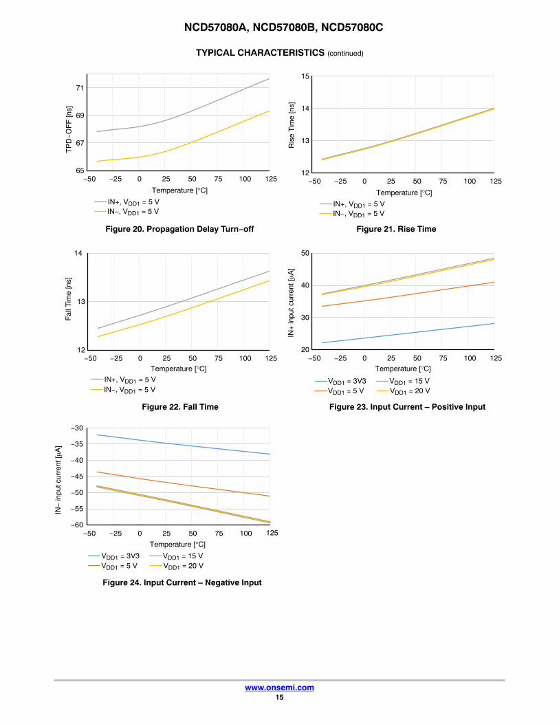
Figure 20. Propagation Delay Turn−off Figure 21. Rise Time
Figure 22. Fall Time
12
13
14
−50 −25 0 25 50 75 100 125
IN+, VDD1 = 5 VIN−, VDD1 = 5 V
20
30
40
50
−50 −25 0 25 50 75 100 125
IN+
inpu
t cur
rent
[�A
]
VDD1 = 3V3VDD1 = 5 V
VDD1 = 15 VVDD1 = 20 V
Temperature [°C]
Fal
l Tim
e [n
s]
Temperature [°C]
−60
−55
−50
−45
−40
−35
−30
−50 −25 0 25 50 75 100 125
Temperature [°C]
IN−
inpu
t cur
rent
[�A
]
VDD1 = 3V3VDD1 = 5 V
VDD1 = 15 VVDD1 = 20 V
Figure 23. Input Current – Positive Input
12
13
14
15
−50 −25 0 25 50 75 100 125
IN+, VDD1 = 5 VIN−, VDD1 = 5 V
Ris
e Ti
me
[ns]
Temperature [°C]
65
67
69
71
−50 −25 0 25 50 75 100 125
IN+, VDD1 = 5 VIN−, VDD1 = 5 V
Temperature [°C]
TP
D−
OF
F [n
s]
Figure 24. Input Current – Negative Input

NCD57080A, NCD57080B, NCD57080C
www.onsemi.com16
Under Voltage Lockout (Refer to Figure 8A/8B/8C/8D)UVLO ensures correct switching of IGBT connected to
the driver output.• The IGBT is turned−off and the output is disabled, if
the supply VDD1 drops below VUVLO1−OUT−OFF orVDD2 drops below VUVLO2−OUT−OFF.
• The driver output does not follow the input signal onIN+ or IN− until the VDDX rises above theVUVLOX−OUT−ON and the input signal rising edge isapplied to the IN+ or IN−
• VEE2 is not monitored (NCD57080B)
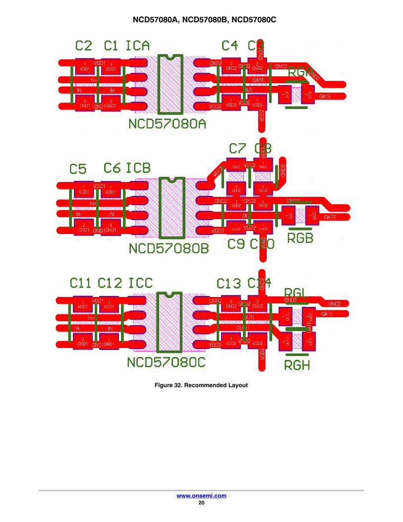
With high loading gate capacitances over 10 nF it isimportant to follow the decoupling capacitor routingguidelines as shown on Figure 32. The decoupling capacitorvalue should be at least 10 �F. Also gate resistor of minimal
value of 2 � has to be used in order to avoid interference ofthe high di/dt with internal circuitry (e.g. UVLO2).
After the power−on of the driver there has to be a risingedge applied to the IN+ or falling edge to the IN− in orderfor the output to start following the inputs. This serves as aprotection against producing partial pulses at the output ifthe VDD1 or VDD2 is applied in the middle of the input PWMpulse.
If the VDD2 rises over VUVLO−OUT−ON level the PWMwill appear on the output after tUVR2 + tUVR2−spread. ThetUVR2−spread time is variable and is defined as a time fromend of tUVR2 to first rising edge on IN+ input. If the VDD2is starting from 0 V the time until PWM is at the output ofthe driver is longer than tUVR2 + tUVR2−spread. This is causedby start up time of internal circuits of the driver.
NCD57080A, NCD57080B, NCD57080C
www.onsemi.com17
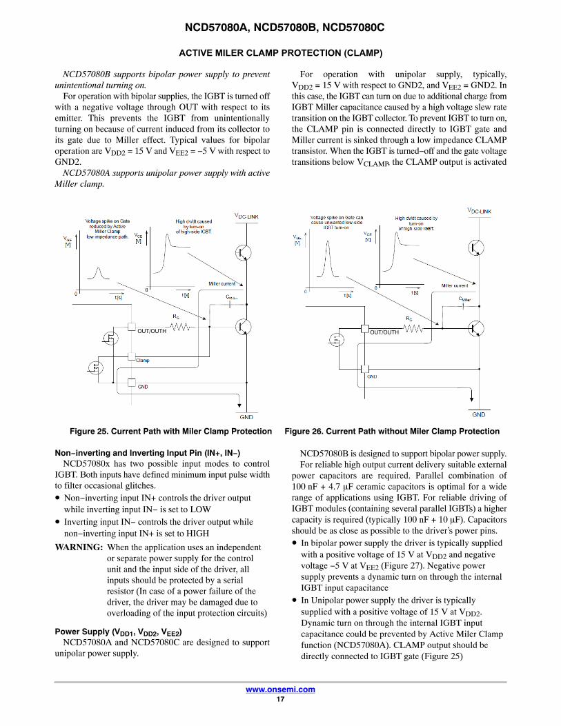
ACTIVE MILER CLAMP PROTECTION (CLAMP)
NCD57080B supports bipolar power supply to preventunintentional turning on.
For operation with bipolar supplies, the IGBT is turned offwith a negative voltage through OUT with respect to itsemitter. This prevents the IGBT from unintentionallyturning on because of current induced from its collector toits gate due to Miller effect. Typical values for bipolaroperation are VDD2 = 15 V and VEE2 = −5 V with respect toGND2.
NCD57080A supports unipolar power supply with activeMiller clamp.
For operation with unipolar supply, typically,VDD2 = 15 V with respect to GND2, and VEE2 = GND2. Inthis case, the IGBT can turn on due to additional charge fromIGBT Miller capacitance caused by a high voltage slew ratetransition on the IGBT collector. To prevent IGBT to turn on,the CLAMP pin is connected directly to IGBT gate andMiller current is sinked through a low impedance CLAMPtransistor. When the IGBT is turned−off and the gate voltagetransitions below VCLAMP, the CLAMP output is activated
Figure 25. Current Path with Miler Clamp Protection Figure 26. Current Path without Miler Clamp Protection
OUT/OUTH OUT/OUTH
Non−inverting and Inverting Input Pin (IN+, IN−)NCD57080x has two possible input modes to control
IGBT. Both inputs have defined minimum input pulse widthto filter occasional glitches.• Non−inverting input IN+ controls the driver output
while inverting input IN− is set to LOW• Inverting input IN− controls the driver output while
non−inverting input IN+ is set to HIGH
WARNING: When the application uses an independentor separate power supply for the controlunit and the input side of the driver, allinputs should be protected by a serialresistor (In case of a power failure of thedriver, the driver may be damaged due tooverloading of the input protection circuits)
Power Supply (VDD1, VDD2, VEE2)NCD57080A and NCD57080C are designed to support
unipolar power supply.
NCD57080B is designed to support bipolar power supply.For reliable high output current delivery suitable external
power capacitors are required. Parallel combination of100 nF + 4.7 �F ceramic capacitors is optimal for a widerange of applications using IGBT. For reliable driving ofIGBT modules (containing several parallel IGBTs) a highercapacity is required (typically 100 nF + 10 �F). Capacitorsshould be as close as possible to the driver’s power pins.• In bipolar power supply the driver is typically supplied
with a positive voltage of 15 V at VDD2 and negativevoltage −5 V at VEE2 (Figure 27). Negative powersupply prevents a dynamic turn on through the internalIGBT input capacitance
• In Unipolar power supply the driver is typicallysupplied with a positive voltage of 15 V at VDD2.Dynamic turn on through the internal IGBT inputcapacitance could be prevented by Active Miler Clampfunction (NCD57080A). CLAMP output should bedirectly connected to IGBT gate (Figure 25)

NCD57080A, NCD57080B, NCD57080C
www.onsemi.com18
Figure 27. Bipolar Power Supply NCD57080B
VDD1
IN +
IN -
GND 1
VEE2
GND2
OUT
VDD2
+
-
VDD210 µF
+
-
VDD1
100 n
100 n
10 µF
+
- VEE210 µF 100 n
Figure 28. Unipolar Power Supply NCD57080A
VDD1
IN+
IN-
GND1
GND2
CLAMP
OUT
VDD2
+
-
VDD210µF
+
-
VDD1
100 n
100 n
10 µF
Figure 29. Suggested Bypassing Scheme for NCD57080x
VDD1
IN+
IN-
GND1
GND2
OUTL
OUTH
VDD2
+
-
VDD210 µF
+
-
VDD1
100 n
100 n
10 µF
NCD57080A, NCD57080B, NCD57080C
www.onsemi.com19
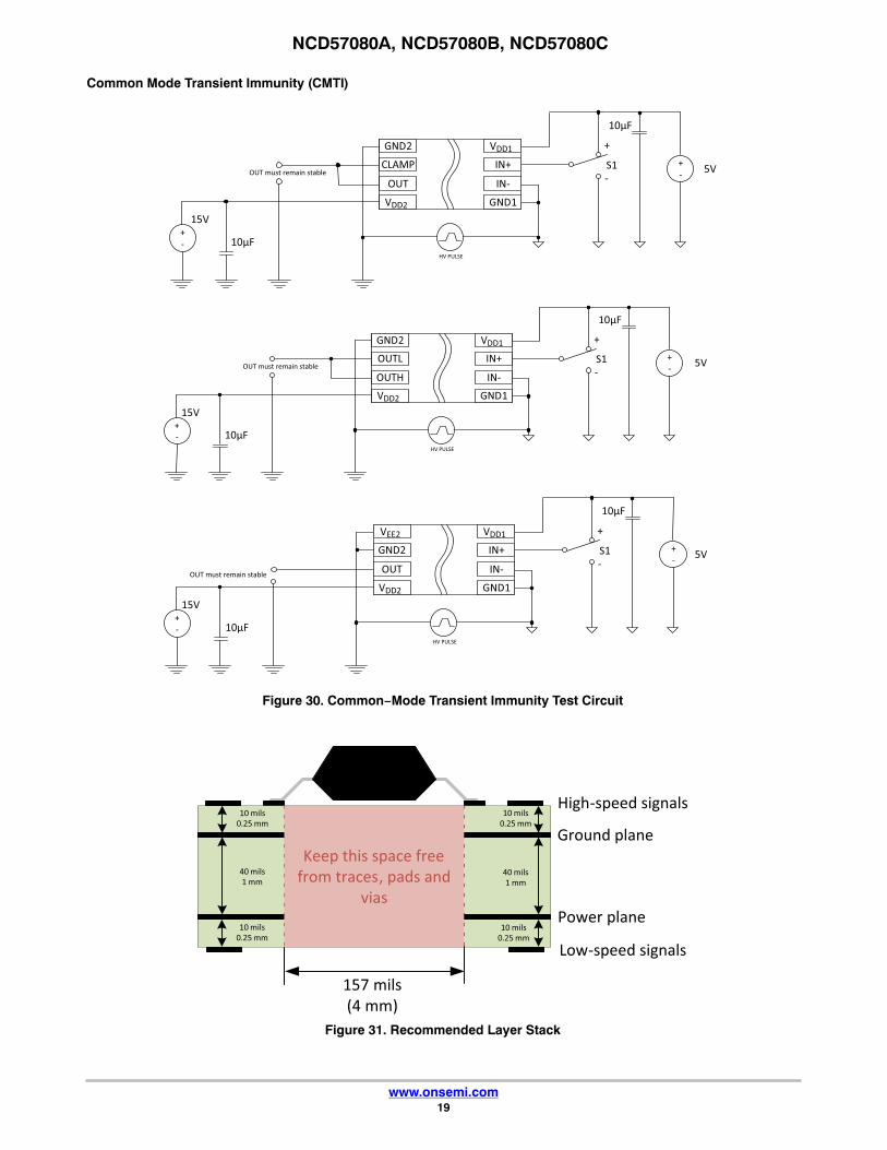
Common Mode Transient Immunity (CMTI)
Figure 30. Common−Mode Transient Immunity Test Circuit
+
-
15V
OUT must remain stable
10µF
+
-
10µF
S1 5V
+
-
HV PULSE
VDD1
IN+
IN-
GND1
GND2
CLAMP
OUT
VDD2
+
-
15V
OUT must remain stable
10µF
+
-
10µF
S1
+
-
HV PULSE
VDD1
IN+
IN-
GND1
GND2
OUTL
OUTH
VDD2
5V
+
-
15V
OUT must remain stable
10µF
+
-
10µF
S1
+
-
HV PULSE
VDD1
IN+
IN-
GND1
VEE2
GND2
OUT
VDD2
5V
Figure 31. Recommended Layer Stack
10 mils
0.25 mm
Keep this space free
from traces, pads and
vias
10 mils
0.25 mm
10 mils
0.25 mm
10 mils
0.25 mm
10 mils
0.25 mm
40 mils
1 mm40 mils
1 mm
157 mils
(4 mm)
High-speed signals
Low-speed signals
Ground plane
Power plane
NCD57080A, NCD57080B, NCD57080C
www.onsemi.com20
Figure 32. Recommended Layout

NCD57080A, NCD57080B, NCD57080C
www.onsemi.com21
ORDERING INFORMATION
Device Package Shipping†
NCD57080ADR2G SOIC−8 Narrow Body, (Pb−Free) 2500 / Tape & Reel
NCD57080BDR2G(In Development)
SOIC−8 Narrow Body, (Pb−Free) 2500 / Tape & Reel
NCD57080CDR2G SOIC−8 Narrow Body, (Pb−Free) 2500 / Tape & Reel
†For information on tape and reel specifications, including part orientation and tape sizes, please refer to our Tape and Reel PackagingSpecifications Brochure, BRD8011/D.

SOIC−8 NBCASE 751−07
ISSUE AKDATE 16 FEB 2011
SEATINGPLANE
14
58
N
J
X 45�
K
NOTES:1. DIMENSIONING AND TOLERANCING PER
ANSI Y14.5M, 1982.2. CONTROLLING DIMENSION: MILLIMETER.3. DIMENSION A AND B DO NOT INCLUDE
MOLD PROTRUSION.4. MAXIMUM MOLD PROTRUSION 0.15 (0.006)
PER SIDE.5. DIMENSION D DOES NOT INCLUDE DAMBAR
PROTRUSION. ALLOWABLE DAMBARPROTRUSION SHALL BE 0.127 (0.005) TOTALIN EXCESS OF THE D DIMENSION ATMAXIMUM MATERIAL CONDITION.
6. 751−01 THRU 751−06 ARE OBSOLETE. NEWSTANDARD IS 751−07.
A
B S
DH
C
0.10 (0.004)
SCALE 1:1
STYLES ON PAGE 2
DIMA
MIN MAX MIN MAXINCHES
4.80 5.00 0.189 0.197
MILLIMETERS
B 3.80 4.00 0.150 0.157C 1.35 1.75 0.053 0.069D 0.33 0.51 0.013 0.020G 1.27 BSC 0.050 BSCH 0.10 0.25 0.004 0.010J 0.19 0.25 0.007 0.010K 0.40 1.27 0.016 0.050M 0 8 0 8 N 0.25 0.50 0.010 0.020S 5.80 6.20 0.228 0.244
−X−
−Y−
G
MYM0.25 (0.010)
−Z−
YM0.25 (0.010) Z S X S
M� � � �
XXXXX = Specific Device CodeA = Assembly LocationL = Wafer LotY = YearW = Work Week� = Pb−Free Package
GENERICMARKING DIAGRAM*
1
8
XXXXXALYWX
1
8
IC Discrete
XXXXXXAYWW
�1
8
1.520.060
7.00.275
0.60.024
1.2700.050
4.00.155
� mminches
�SCALE 6:1
*For additional information on our Pb−Free strategy and solderingdetails, please download the ON Semiconductor Soldering andMounting Techniques Reference Manual, SOLDERRM/D.
SOLDERING FOOTPRINT*
Discrete
XXXXXXAYWW
1
8
(Pb−Free)
XXXXXALYWX
�1
8
IC(Pb−Free)
XXXXXX = Specific Device CodeA = Assembly LocationY = YearWW = Work Week� = Pb−Free Package
*This information is generic. Please refer todevice data sheet for actual part marking.Pb−Free indicator, “G” or microdot “�”, mayor may not be present. Some products maynot follow the Generic Marking.
MECHANICAL CASE OUTLINE
PACKAGE DIMENSIONS
ON Semiconductor and are trademarks of Semiconductor Components Industries, LLC dba ON Semiconductor or its subsidiaries in the United States and/or other countries.ON Semiconductor reserves the right to make changes without further notice to any products herein. ON Semiconductor makes no warranty, representation or guarantee regardingthe suitability of its products for any particular purpose, nor does ON Semiconductor assume any liability arising out of the application or use of any product or circuit, and specificallydisclaims any and all liability, including without limitation special, consequential or incidental damages. ON Semiconductor does not convey any license under its patent rights nor therights of others.
98ASB42564BDOCUMENT NUMBER:
DESCRIPTION:
Electronic versions are uncontrolled except when accessed directly from the Document Repository.Printed versions are uncontrolled except when stamped “CONTROLLED COPY” in red.
PAGE 1 OF 2SOIC−8 NB
© Semiconductor Components Industries, LLC, 2019 www.onsemi.com
SOIC−8 NBCASE 751−07
ISSUE AKDATE 16 FEB 2011
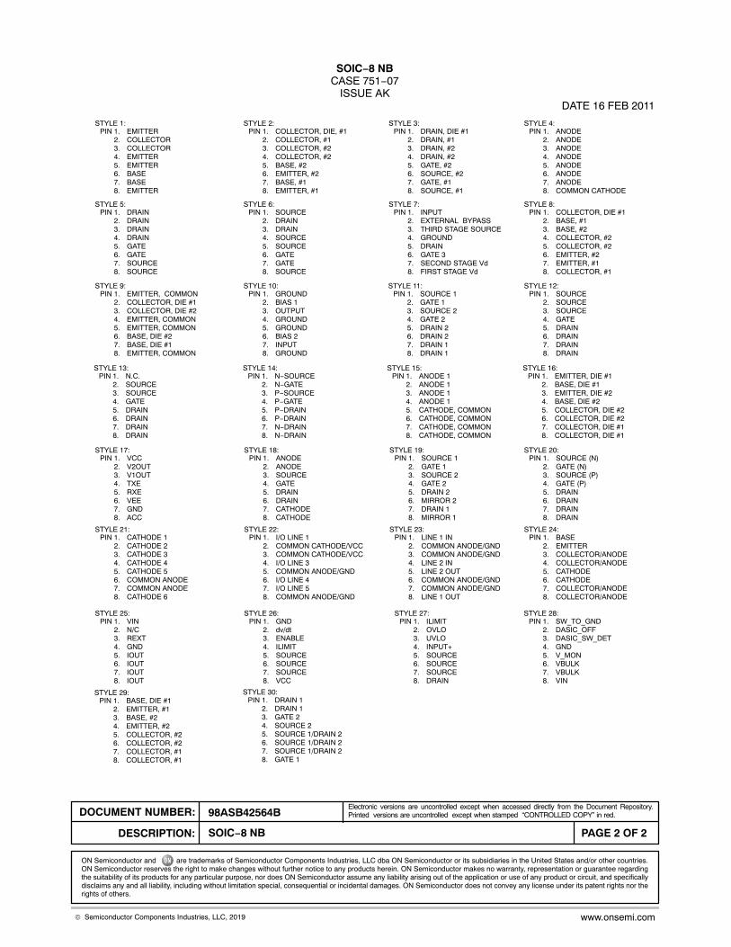
STYLE 4:PIN 1. ANODE
2. ANODE3. ANODE4. ANODE5. ANODE6. ANODE7. ANODE8. COMMON CATHODE
STYLE 1:PIN 1. EMITTER
2. COLLECTOR3. COLLECTOR4. EMITTER5. EMITTER6. BASE7. BASE8. EMITTER
STYLE 2:PIN 1. COLLECTOR, DIE, #1
2. COLLECTOR, #13. COLLECTOR, #24. COLLECTOR, #25. BASE, #26. EMITTER, #27. BASE, #18. EMITTER, #1
STYLE 3:PIN 1. DRAIN, DIE #1
2. DRAIN, #13. DRAIN, #24. DRAIN, #25. GATE, #26. SOURCE, #27. GATE, #18. SOURCE, #1
STYLE 6:PIN 1. SOURCE
2. DRAIN3. DRAIN4. SOURCE5. SOURCE6. GATE7. GATE8. SOURCE
STYLE 5:PIN 1. DRAIN
2. DRAIN3. DRAIN4. DRAIN5. GATE6. GATE7. SOURCE8. SOURCE
STYLE 7:PIN 1. INPUT
2. EXTERNAL BYPASS3. THIRD STAGE SOURCE4. GROUND5. DRAIN6. GATE 37. SECOND STAGE Vd8. FIRST STAGE Vd
STYLE 8:PIN 1. COLLECTOR, DIE #1
2. BASE, #13. BASE, #24. COLLECTOR, #25. COLLECTOR, #26. EMITTER, #27. EMITTER, #18. COLLECTOR, #1
STYLE 9:PIN 1. EMITTER, COMMON
2. COLLECTOR, DIE #13. COLLECTOR, DIE #24. EMITTER, COMMON5. EMITTER, COMMON6. BASE, DIE #27. BASE, DIE #18. EMITTER, COMMON
STYLE 10:PIN 1. GROUND
2. BIAS 13. OUTPUT4. GROUND5. GROUND6. BIAS 27. INPUT8. GROUND
STYLE 11:PIN 1. SOURCE 1
2. GATE 13. SOURCE 24. GATE 25. DRAIN 26. DRAIN 27. DRAIN 18. DRAIN 1
STYLE 12:PIN 1. SOURCE
2. SOURCE3. SOURCE4. GATE5. DRAIN6. DRAIN7. DRAIN8. DRAIN
STYLE 14:PIN 1. N−SOURCE
2. N−GATE3. P−SOURCE4. P−GATE5. P−DRAIN6. P−DRAIN7. N−DRAIN8. N−DRAIN
STYLE 13:PIN 1. N.C.
2. SOURCE3. SOURCE4. GATE5. DRAIN6. DRAIN7. DRAIN8. DRAIN
STYLE 15:PIN 1. ANODE 1
2. ANODE 13. ANODE 14. ANODE 15. CATHODE, COMMON6. CATHODE, COMMON7. CATHODE, COMMON8. CATHODE, COMMON
STYLE 16:PIN 1. EMITTER, DIE #1
2. BASE, DIE #13. EMITTER, DIE #24. BASE, DIE #25. COLLECTOR, DIE #26. COLLECTOR, DIE #27. COLLECTOR, DIE #18. COLLECTOR, DIE #1
STYLE 17:PIN 1. VCC
2. V2OUT3. V1OUT4. TXE5. RXE6. VEE7. GND8. ACC
STYLE 18:PIN 1. ANODE
2. ANODE3. SOURCE4. GATE5. DRAIN6. DRAIN7. CATHODE8. CATHODE
STYLE 19:PIN 1. SOURCE 1
2. GATE 13. SOURCE 24. GATE 25. DRAIN 26. MIRROR 27. DRAIN 18. MIRROR 1
STYLE 20:PIN 1. SOURCE (N)
2. GATE (N)3. SOURCE (P)4. GATE (P)5. DRAIN6. DRAIN7. DRAIN8. DRAIN
STYLE 21:PIN 1. CATHODE 1
2. CATHODE 23. CATHODE 34. CATHODE 45. CATHODE 56. COMMON ANODE7. COMMON ANODE8. CATHODE 6
STYLE 22:PIN 1. I/O LINE 1
2. COMMON CATHODE/VCC3. COMMON CATHODE/VCC4. I/O LINE 35. COMMON ANODE/GND6. I/O LINE 47. I/O LINE 58. COMMON ANODE/GND
STYLE 23:PIN 1. LINE 1 IN
2. COMMON ANODE/GND3. COMMON ANODE/GND4. LINE 2 IN5. LINE 2 OUT6. COMMON ANODE/GND7. COMMON ANODE/GND8. LINE 1 OUT
STYLE 24:PIN 1. BASE
2. EMITTER3. COLLECTOR/ANODE4. COLLECTOR/ANODE5. CATHODE6. CATHODE7. COLLECTOR/ANODE8. COLLECTOR/ANODE
STYLE 25:PIN 1. VIN
2. N/C3. REXT4. GND5. IOUT6. IOUT7. IOUT8. IOUT
STYLE 26:PIN 1. GND
2. dv/dt3. ENABLE4. ILIMIT5. SOURCE6. SOURCE7. SOURCE8. VCC
STYLE 27:PIN 1. ILIMIT
2. OVLO3. UVLO4. INPUT+5. SOURCE6. SOURCE7. SOURCE8. DRAIN
STYLE 28:PIN 1. SW_TO_GND
2. DASIC_OFF3. DASIC_SW_DET4. GND5. V_MON6. VBULK7. VBULK8. VIN
STYLE 29:PIN 1. BASE, DIE #1
2. EMITTER, #13. BASE, #24. EMITTER, #25. COLLECTOR, #26. COLLECTOR, #27. COLLECTOR, #18. COLLECTOR, #1
STYLE 30:PIN 1. DRAIN 1
2. DRAIN 13. GATE 24. SOURCE 25. SOURCE 1/DRAIN 26. SOURCE 1/DRAIN 27. SOURCE 1/DRAIN 28. GATE 1
ON Semiconductor and are trademarks of Semiconductor Components Industries, LLC dba ON Semiconductor or its subsidiaries in the United States and/or other countries.ON Semiconductor reserves the right to make changes without further notice to any products herein. ON Semiconductor makes no warranty, representation or guarantee regardingthe suitability of its products for any particular purpose, nor does ON Semiconductor assume any liability arising out of the application or use of any product or circuit, and specificallydisclaims any and all liability, including without limitation special, consequential or incidental damages. ON Semiconductor does not convey any license under its patent rights nor therights of others.
98ASB42564BDOCUMENT NUMBER:
DESCRIPTION:
Electronic versions are uncontrolled except when accessed directly from the Document Repository.Printed versions are uncontrolled except when stamped “CONTROLLED COPY” in red.
PAGE 2 OF 2SOIC−8 NB
© Semiconductor Components Industries, LLC, 2019 www.onsemi.com
www.onsemi.com1
ON Semiconductor and are trademarks of Semiconductor Components Industries, LLC dba ON Semiconductor or its subsidiaries in the United States and/or other countries.ON Semiconductor owns the rights to a number of patents, trademarks, copyrights, trade secrets, and other intellectual property. A listing of ON Semiconductor’s product/patentcoverage may be accessed at www.onsemi.com/site/pdf/Patent−Marking.pdf. ON Semiconductor reserves the right to make changes without further notice to any products herein.ON Semiconductor makes no warranty, representation or guarantee regarding the suitability of its products for any particular purpose, nor does ON Semiconductor assume any liabilityarising out of the application or use of any product or circuit, and specifically disclaims any and all liability, including without limitation special, consequential or incidental damages.Buyer is responsible for its products and applications using ON Semiconductor products, including compliance with all laws, regulations and safety requirements or standards,regardless of any support or applications information provided by ON Semiconductor. “Typical” parameters which may be provided in ON Semiconductor data sheets and/orspecifications can and do vary in different applications and actual performance may vary over time. All operating parameters, including “Typicals” must be validated for each customerapplication by customer’s technical experts. ON Semiconductor does not convey any license under its patent rights nor the rights of others. ON Semiconductor products are notdesigned, intended, or authorized for use as a critical component in life support systems or any FDA Class 3 medical devices or medical devices with a same or similar classificationin a foreign jurisdiction or any devices intended for implantation in the human body. Should Buyer purchase or use ON Semiconductor products for any such unintended or unauthorizedapplication, Buyer shall indemnify and hold ON Semiconductor and its officers, employees, subsidiaries, affiliates, and distributors harmless against all claims, costs, damages, andexpenses, and reasonable attorney fees arising out of, directly or indirectly, any claim of personal injury or death associated with such unintended or unauthorized use, even if suchclaim alleges that ON Semiconductor was negligent regarding the design or manufacture of the part. ON Semiconductor is an Equal Opportunity/Affirmative Action Employer. Thisliterature is subject to all applicable copyright laws and is not for resale in any manner.
PUBLICATION ORDERING INFORMATIONTECHNICAL SUPPORTNorth American Technical Support:Voice Mail: 1 800−282−9855 Toll Free USA/CanadaPhone: 011 421 33 790 2910
LITERATURE FULFILLMENT:Email Requests to: [email protected]
ON Semiconductor Website: www.onsemi.com
Europe, Middle East and Africa Technical Support:Phone: 00421 33 790 2910For additional information, please contact your local Sales Representative
◊

Mouser Electronics
Authorized Distributor
Click to View Pricing, Inventory, Delivery & Lifecycle Information: onsemi:
NCD57080ADR2G NCD57080CDR2G NCV57080ADR2G NCV57080CDR2G NCD57080BDR2G
NCV57080BDR2G