Embed Size (px)
Citation preview

NAVAL
POSTGRADUATE SCHOOL
MONTEREY, CALIFORNIA
THESIS
Approved for public release; distribution is unlimited
EVALUATION OF WIDEBAND LEAKAGE CANCELLATION CIRCUIT FOR IMPROVED TRANSMIT-
RECEIVE ISOLATION
by
Pek, Wee Kok
December 2011
Thesis Advisor: David C. Jenn Second Reader: Ric Romero

THIS PAGE INTENTIONALLY LEFT BLANK

i
REPORT DOCUMENTATION PAGE Form Approved OMB No. 0704-0188 Public reporting burden for this collection of information is estimated to average 1 hour per response, including the time for reviewing instruction, searching existing data sources, gathering and maintaining the data needed, and completing and reviewing the collection of information. Send comments regarding this burden estimate or any other aspect of this collection of information, including suggestions for reducing this burden, to Washington headquarters Services, Directorate for Information Operations and Reports, 1215 Jefferson Davis Highway, Suite 1204, Arlington, VA 22202-4302, and to the Office of Management and Budget, Paperwork Reduction Project (0704-0188) Washington DC 20503. 1. AGENCY USE ONLY (Leave blank)
2. REPORT DATE December 2011
3. REPORT TYPE AND DATES COVERED Master’s Thesis
4. TITLE AND SUBTITLE Evaluation of Wideband Leakage Cancellation Circuit for Improved Transmit-Receive Isolation
5. FUNDING NUMBERS
6. AUTHOR(S) Pek, Wee Kok 7. PERFORMING ORGANIZATION NAME(S) AND ADDRESS(ES)
Naval Postgraduate School Monterey, CA 93943-5000
8. PERFORMING ORGANIZATION REPORT NUMBER
9. SPONSORING /MONITORING AGENCY NAME(S) AND ADDRESS(ES) N/A
10. SPONSORING/MONITORING AGENCY REPORT NUMBER
11. SUPPLEMENTARY NOTES The views expressed in this thesis are those of the author and do not reflect the official policy or position of the Department of Defense or the U.S. Government. IRB Protocol number ______N/A______.
12a. DISTRIBUTION / AVAILABILITY STATEMENT Approved for public release; distribution is unlimited
12b. DISTRIBUTION CODE A
13. ABSTRACT (maximum 200 words) The objective of this thesis is to improve the cancellation performance of a wideband leakage cancellation circuit (WLCC). The results of this thesis can be applied to any sensor or communication system that simultaneously transmits and receives, for example, continuous wave (CW) radar, frequency modulated continuous wave (FMCW) radar, or a wirelessly networked distributed digital phased array (WNDDPA), where the isolation is required between the transmit and receive paths.
The approach is to investigate leakage cancellation circuit (LCC) techniques in the analog domain. A frequency demultiplexing and multiplexing circuit (FDMC) is adopted for the analog study and is simulated using Advanced Design System 2011.05 (ADS). Both narrowband and wideband LCC models are simulated in ADS to investigate their phase and amplitude balance properties. Methods such as applying grounded stubs to match the phase slopes of the cancellation and leakage paths are also investigated.
Two sets of grounded shunt stubs with different characteristics are applied on the leakage and cancellation paths to achieve near coherent cancellation. Using this configuration, the maximum cancellation power of the LCC is about 87 dB, and the 3.0 dB bandwidth of the cancellation is about 56 MHz. 14. SUBJECT TERMS Transmit Receive Isolation, wideband, leakage cancellation 15. NUMBER OF
PAGES 101
16. PRICE CODE
17. SECURITY CLASSIFICATION OF REPORT
Unclassified
18. SECURITY CLASSIFICATION OF THIS PAGE
Unclassified
19. SECURITY CLASSIFICATION OF ABSTRACT
Unclassified
20. LIMITATION OF ABSTRACT
UU NSN 7540-01-280-5500 Standard Form 298 (Rev. 2-89) Prescribed by ANSI Std. 239-18

ii
THIS PAGE INTENTIONALLY LEFT BLANK

iii
Approved for public release; distribution is unlimited
EVALUATION OF WIDEBAND LEAKAGE CANCELLATION CIRCUIT FOR IMPROVED TRANSMIT-RECEIVE ISOLATION
Pek, Wee Kok Civilian, Singapore Technologies Dynamics Pte Ltd
B.Eng, National University of Singapore, 1998
Submitted in partial fulfillment of the requirements for the degree of
MASTER OF SCIENCE IN ELECTRICAL ENGINEERING
from the
NAVAL POSTGRADUATE SCHOOL December 2011
Author: Pek, Wee Kok
Approved by: David C. Jenn Thesis Advisor
Ric Romero Second Reader
R. Clark Robertson Chair, Department of Electrical and Computer Engineering

iv
THIS PAGE INTENTIONALLY LEFT BLANK

v
ABSTRACT
The objective of this thesis is to improve the cancellation performance of a wideband
leakage cancellation circuit (WLCC). The results of this thesis can be applied to any
sensor or communication system that simultaneously transmits and receives, for example,
continuous wave (CW) radar, a frequency modulated continuous wave (FMCW) radar, or
a wirelessly networked distributed digital phased array (WNDDPA), where isolation is
required between the transmit and receive paths.
The approach is to investigate leakage cancellation circuit (LCC) techniques in
the analog domain. A frequency demultiplexing and multiplexing circuit (FDMC) is
adopted for the analog study and is simulated using Advanced Design System 2011.05
(ADS). Both narrowband and wideband LCC models are simulated in ADS to
investigate their phase and amplitude balance properties. Methods such as applying
grounded stubs to match the phase slopes of the cancellation and leakage paths are also
investigated.
Two sets of grounded shunt stubs with different characteristics are applied on the
leakage and cancellation paths to achieve near coherent cancellation. Using this
configuration, the maximum cancellation power of the LCC is about 87 dB, and the 3.0
dB bandwidth of the cancellation is about 56 MHz.

vi
THIS PAGE INTENTIONALLY LEFT BLANK

vii
TABLE OF CONTENTS
I. INTRODUCTION........................................................................................................1 A. BACKGROUND ..............................................................................................1
1. Leakage Problem in CW and FMCW Radars ..................................2 2. Isolation of Transmit and Receive Signals ........................................2 3. Amplitude and Phase Imbalance in LCC ..........................................4 4. Wideband Leakage Cancellation Circuit...........................................7
B OBJECTIVE ....................................................................................................8 C. SCOPE AND ORGANIZATION ...................................................................9
II. IDEAL LCC SIMULATION ....................................................................................11 A. INTRODUCTION..........................................................................................11 B. IDEAL LCC SIMULATION ........................................................................11 C. EFFECTS OF ANTENNA MISMATCH ....................................................15 D. EFFECTS OF SIGNAL POWER.................................................................18 E. EFFECTS OF NON-IDEAL COMPONENTS ...........................................20
1. Non-ideal Power Splitter ...................................................................21 2. Non-ideal Circulator ..........................................................................23 3. Non-ideal Phase Shifter .....................................................................24
F. SUMMARY ....................................................................................................29
III. WIDEBAND LCC ......................................................................................................31 A. INTRODUCTION..........................................................................................31 B. RESPONSE OF WLCC ................................................................................33
1. Magnitude Response of the Residual Signal ....................................33 2. Effects of Phase Imbalance ...............................................................37
C. PHASE SLOPE ALIGNMENT ....................................................................39 1. Concept of Phase Slope Alignment ...................................................39 2. Shunt Stub Circuit for Phase Slope Alignment ...............................40 3. Application of Shunt Stub Circuit to the Leakage Path .................45 4. Application of Shunt Stub Circuit to the Cancellation and
Leakage Paths.....................................................................................48 5. Mismatch Effects of a Dipole Antenna.............................................54 6. Application of Spiral Antenna ..........................................................59
D. SUMMARY ....................................................................................................68
IV. SUMMARY, CONCLUSIONS, AND RECOMMENDATIONS ..........................71 A. SUMMARY ....................................................................................................71 B. CONCLUSIONS ............................................................................................72 C. RECOMMENDATIONS ...............................................................................73
1. Broadbanding Techniques for Antenna Impedance Matching .....73 2. Modeling of Transmit and Receive Module ....................................73 3. Modeling with ADS Transient Simulator ........................................73 4. Hardware Prototype ..........................................................................73

viii
LIST OF REFERENCES ......................................................................................................75
INITIAL DISTRIBUTION LIST .........................................................................................77

ix
LIST OF FIGURES
Figure 1. Basic principle of range computation in FMCW radar (From [1]). ...................1 Figure 2. Operation of LCC (From [9]). ...........................................................................4 Figure 3. Basic LCC configuration model (From [9]). .....................................................4 Figure 4. Effects of phase and amplitude imbalance (From [9]).......................................6 Figure 5. Frequency response of LCC (From [11]). ..........................................................6 Figure 6. Block diagram of WLCC (From [9]). ................................................................7 Figure 7. Conceptual frequency response of WLCC versus LCC (From [9]). .................8 Figure 8. Ideal LCC model in ADS (After [9], [11]). .....................................................12 Figure 9. Scattering parameter S31 versus that variation of attenuation sweep
variable X. ........................................................................................................13 Figure 10. Magnitude of transmission coefficient from Port 1 to Port 3 versus
frequency..........................................................................................................14 Figure 11. Phase of transmission coefficient from Port 1 to Port 3 versus frequency. ....14 Figure 12. LCC model for load mismatch simulation. ......................................................15 Figure 13. Magnitude of S31 versus LCC attenuation X at various load impedance
(After [9]). ........................................................................................................16 Figure 14. Magnitude of S31 versus frequency for impedance mismatch case. ................17 Figure 15. Phase of S31 versus frequency for impedance mismatch case. ........................17 Figure 16. Simulation model for receiver power study (After [9]). ..................................19 Figure 17. Variation of residual power versus received power. ........................................20 Figure 18. Settings for a realistic power splitter modeling. ..............................................22 Figure 19. Magnitude of S31 under the influence of non-ideal power splitter...................22 Figure 20. Setting for more realistic circulator modeling. ................................................23 Figure 21. Magnitude of S31 under the influence of non-ideal circulator and power
splitter. .............................................................................................................24 Figure 22. Settings for non-ideal phase shifter..................................................................25 Figure 23. Simulation model for non-ideal components. ..................................................26 Figure 24. Effects of non-ideal components on magnitude of S31. ...................................27 Figure 25. Magnitude of S31 parameter versus frequency with non-ideal components. ...28 Figure 26. Phase of S31 versus frequency with non-ideal components. ............................28 Figure 27. ADS model of WLCC with FDMC using power splitters (After [11]). ..........32 Figure 28. ADS model of WLCC with FDMC using circulators (After [11]). .................33 Figure 29. Amplitude of residual using FDMC with power splitters (After [11]). ...........34 Figure 30. Amplitude of residual signal using FDMC with circulators (After [11]). .......34 Figure 31. Cancellation signal using FDMC with power splitters (After [11]). ...............35 Figure 32. Cancellation signal using FDMC with circulators (After [11]). ......................36 Figure 33. Phase change of signal through WLCC using FDMC with power splitter
versus frequency. .............................................................................................37 Figure 34. Phase change of signal through WLCC using FDMC with circulator
versus frequency. .............................................................................................38 Figure 35. Model of LCC with phase slope alignment. ....................................................39

x
Figure 36. Magnitude of residual power versus attenuation in LCC over frequency of 2.36 GHz and 2.44 GHz. ..................................................................................40
Figure 37. Phase slope alignment circuits consisting of quarter wave length stubs connected in series and parallel. ......................................................................41
Figure 38. Phase response of the quarter wavelength stub phase slope alignment circuit. ..............................................................................................................42
Figure 39. Application of phase slope alignment circuit on LCC with non-ideal circulator. .........................................................................................................46
Figure 40. Plot of residual power versus LCC attenuation. ..............................................47 Figure 41. Application of shunt stub circuits on both cancellation and leakage paths. ....48 Figure 42. Plot of residual power versus LCC attenuation with 2 sets of shunt stubs
circuits. .............................................................................................................49 Figure 43. Phase angles of the leakage and cancellation paths versus frequency. ............50 Figure 44. Magnitude of residual signal versus frequency. ..............................................51 Figure 45. Magnitude responses of phase slope alignment circuits with three quarter
wavelength shunt stubs and quarter wavelength series stubs applied to leakage path. ....................................................................................................52
Figure 46. Magnitude responses of WLCC with phase slope alignment circuits with quarter wavelength shunt stubs and three quarter wavelength series stub. ......53
Figure 47. Cancellation C versus frequency. ....................................................................53 Figure 48. Calculated VSWR as a function of frequency for dipoles of different wire
diameter (From [18])........................................................................................54 Figure 49. ADS model of LCC with a dipole antenna. .....................................................55 Figure 50. Residual signal level with dipole antenna, LCC attenuation of 20 dB. ...........56 Figure 51. Residual signal level with dipole antenna, LCC attenuation of 21.8 dB. ........57 Figure 52. Signal level at the Port 2 of circulator along the antenna path. .......................57 Figure 53. Magnitude of the leakage and cancellation signals with source of 6.0 dBm. ..58 Figure 54. Phase of the leakage and cancellation signals..................................................58 Figure 55. Magnitude of S11 parameter of spiral antenna with frequency. .......................60 Figure 56. Phase responses of the S11 parameter of spiral antenna with frequency. .........61 Figure 57. ADS model of WLCC with spiral antenna. .....................................................61 Figure 58. ADS simulation setting for the spiral antenna model. .....................................62 Figure 59. Syntax of spiral antenna S11 parameter file. .....................................................63 Figure 60. Magnitude of residual signal in dBm with frequency at source power of
6.0 dBm. ...........................................................................................................63 Figure 61. Magnitude of the cancellation and leakage signals..........................................64 Figure 62. Phase of cancellation and leakage signals. ......................................................65 Figure 63. ADS model of modified WLCC with spiral antenna. ......................................66 Figure 64. Magnitude of cancellation and leakage signal with frequency at source
power of 6.0 dBm. ...........................................................................................67 Figure 65. Phase of the cancellation and leakage signals with frequency. .......................67 Figure 66. Magnitude of residual signal with frequency...................................................68

xi
LIST OF TABLES
Table 1. Component specification (After [11]). .............................................................21 Table 2. Variations of phase slope with stub length. .....................................................43 Table 3. Phase slope introduced by various WLCC configurations. .............................44 Table 4. Length of shunt stubs for LCC design. ............................................................45 Table 5. S11 parameters of spiral antenna used for simulation.......................................60

xii
THIS PAGE INTENTIONALLY LEFT BLANK

xiii
LIST OF ACRONYMS AND ABBREVIATIONS
ADS Advanced System Design
ATTEN Attenuator or Attenuation
CW Continuous Wave
ESM Electronic Support Measures
FDMC Frequency Demultiplexing and Multiplexing Circuit
FMCW Frequency Modulated Continuous Wave
LCC Leakage Cancellation Circuit
RF Radio Frequency
TRM Transmit-Receive Module
TERM Termination
WLAN Wireless Local Area Network
WLCC Wideband Leakage Cancellation Circuit
WNDDPA Wireless Network Distributed Digital Phase Array

xiv
THIS PAGE INTENTIONALLY LEFT BLANK
xv
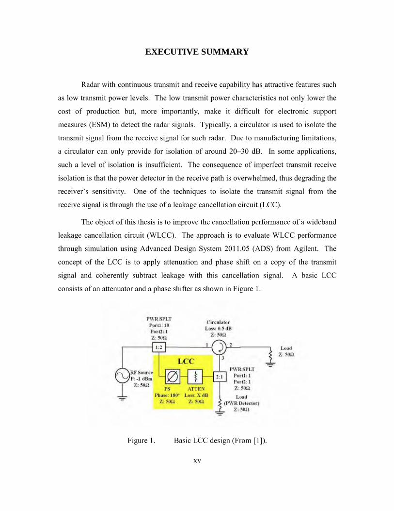
EXECUTIVE SUMMARY
Radar with continuous transmit and receive capability has attractive features such
as low transmit power levels. The low transmit power characteristics not only lower the
cost of production but, more importantly, make it difficult for electronic support
measures (ESM) to detect the radar signals. Typically, a circulator is used to isolate the
transmit signal from the receive signal for such radar. Due to manufacturing limitations,
a circulator can only provide for isolation of around 20–30 dB. In some applications,
such a level of isolation is insufficient. The consequence of imperfect transmit receive
isolation is that the power detector in the receive path is overwhelmed, thus degrading the
receiver’s sensitivity. One of the techniques to isolate the transmit signal from the
receive signal is through the use of a leakage cancellation circuit (LCC).
The object of this thesis is to improve the cancellation performance of a wideband
leakage cancellation circuit (WLCC). The approach is to evaluate WLCC performance
through simulation using Advanced Design System 2011.05 (ADS) from Agilent. The
concept of the LCC is to apply attenuation and phase shift on a copy of the transmit
signal and coherently subtract leakage with this cancellation signal. A basic LCC
consists of an attenuator and a phase shifter as shown in Figure 1.
Figure 1. Basic LCC design (From [1]).

xvi
It is found that hardware limitations degrade the performance of the LCC
significantly. For instance, the phase slope of a phase shifter can narrow the LCC
cancellation bandwidth. When operating beyond the designed center frequency, the
cancellation decreases rapidly, as shown in Figure 2.
Figure 2. Degradation of cancellation with non-ideal components.
In the frequency demultiplexing multiplexing circuit (FDMC) design of WLCC,
the signal is divided into multiple frequency sub-bands and, subsequently, a narrowband
LCC is applied to each frequency sub-band [2]. Elliptic band-pass filters that are applied
in the FDMC WLCC have frequency dependent magnitude and phase responses that are
undesirable. The elliptic band-pass filters introduce amplitude and phase imbalance
between the cancellation and leakage signal. As a result, coherent cancellation cannot be
achieved.
The use of grounded shunt and series stubs as a phase slope alignment circuit is
investigated through simulation. It is proposed to apply shunt and series stubs circuits on
both cancellation and leakage paths, as shown in Figure 3.

xvii
Figure 3. Application of shunt stub circuits on both cancellation and leakage paths
for coherent cancellation.
In order to maintain the magnitude and phase balance, the input signal in the
cancellation path is phase shifted by −270o, and the leakage signal is phase shifted by
−90o. The reason for this configuration is that the phase change and phase slope of stub
circuits follow a discrete form. The cancellation power characteristic of this LCC
configuration is shown in Figure 4.
The maximum cancellation is about 87 dB at 2.38 GHz and 2.42 GHz as shown in
Figure 4, and the 3 dB bandwidth of the cancellation circuit is about 56 MHz. Ideal
coherent cancellation is not achieved due to the slight difference in the magnitude and
phase responses between the stubs circuits used in the two paths.

xviii
Figure 4. Cancellation versus frequency (source power of 6.0 dBm).
The new circuit design increases the cancellation bandwidth. However, it was
found that antenna mismatch can significantly degrade the cancellation circuit
performance. The results of this thesis can be applied to any sensor or communication
system that simultaneously transmits and receives, such as continuous wave (CW) radar,
frequency modulated continuous wave (FMCW) radar or a wirelessly networked
distributed digital phased array (WNDDPA), where isolation and cancellation are
required between the transmit and receive paths.

xix
LIST OF REFERENCES
[1] Wei-Han Cheng, “Cancellation circuit for transmit-receive isolation,” Naval Postgraduate School Master’s Thesis, September 2010.
[2] T. H. Ang, “Conceptual design and software simulation of a wideband leakage cancellation circuit,” Naval Postgraduate School Master’s Thesis, December 2010.

xx
THIS PAGE INTENTIONALLY LEFT BLANK

xxi
ACKNOWLEDGMENTS
I would like to express my gratitude to my thesis advisor, Professor David Jenn
for his valuable time and guidance. I would also like to thank Professor Ric Romero for
his technical expertise and insights as a second reader. I would like to thank Mr. Robert
Broadston for providing his technical expertise and valuable suggestions. I would like to
thank Singapore Technologies Dynamics Pte Ltd for sponsoring me on this master
program. Last, but not least, I thank my wife, Pauline, for her understanding throughout
the master program.

xxii
THIS PAGE INTENTIONALLY LEFT BLANK

1
I. INTRODUCTION
A. BACKGROUND
Radar systems typically illuminate a target with a microwave signal, which is then
reflected and received by a receiving antenna. The radar systems exploit the temporal,
spatial and frequency characteristics of the reflected signal to determine target attributes
such as velocity, range and radar cross section. Signals emitted by radar systems can be
either pulsed or continuous wave. In the case of continuous wave (CW) radar, a
continuous frequency is transmitted. The CW radar makes use of the Doppler shift
between the transmitted and received signal to determine the speed of the target. Since
only a single frequency is transmitted, CW radar is capable of determining the speed of
the target but not its range.
Another class of CW radar is the frequency modulated continuous wave (FMCW)
radar [1]. The FMCW radar transmits a continuous wideband signal over a radio
frequency (RF) band to determine the range of the target. In Figure 1, the basic working
principle of FMCW radar is shown.
Figure 1. Basic principle of range computation in FMCW radar (From [1]).

2
As illustrated in Figure 1, the FMCW radar transmits a frequency modulated
signal that is incident on the target. Part of this RF signal is reflected by the surface of
target. The frequency is swept linearly from f1 to f2. The frequency shift between the
transmitted signal and the received reflected signal is used to compute the range of the
target. As shown in Figure 1, Δf represents the change in frequency between the
transmitted and received signal and T is the duration of the frequency sweep. The range
of the target can be determined from
( )2 12fTcR
f f∆
=−
(1)
where c = 3x10⁸ ms-1 is the velocity of light in free space. As it can be seen in Equation
(1), it is generally desirable to implement a radar system with a frequency band that is as
wide as possible for better range resolution. Such attributes are difficult to implement in
practice due to the limitation in hardware components.
1. Leakage Problem in CW and FMCW Radars
CW and FMCW radars typically do not emit distinct pulses of microwave energy
compared to pulsed radar. As a result, the low transmit power levels make it difficult for
electronic support measures (ESM) to detect the radar’s signal [2]. A disadvantage is that
the continuous transmit and receive nature of the CW and FMCW radar allows undesired
leakage of the transmitted signal directly to the receiver since there is no temporal
separation between the two signals. This direct leakage of the transmitter power onto the
receiver input reduces the performance of the CW radar as the receiver is desensitized.
2. Isolation of Transmit and Receive Signals
For CW radar with a single antenna configuration, isolation can be obtained by
using a hybrid junction, circulator, turnstile junction, or with separate polarizations [3].
As explained in [3], typical isolation through hybrid junction is of the order of 20 to 30
dB and perhaps 60 dB or more with extreme precision. One of the limitations of a hybrid
junction is the inherent loss of half of the transmit power and half of the receive power.

3
In [4], a circulator is designed to minimize return losses and achieve isolation of 20 to 30
dB between the three terminals of the circulator.
Use of separate antennas for transmit and receive is proposed in [5]. Two
cylindrical spiral antennas with oppositely directed windings are used by the authors so
that the transmitted channel is orthogonal to that of the received channel. The two
antennas are physically separated and their separation is comparable to the wavelength of
the transmission. Such technique is only applicable in cases where a two antenna
configuration can be deployed.
An analog leakage cancellation circuit can be added to suppress leakage [6]. This
technique involves continuous tracking of the amplitude and the phase of leakage signal.
In order to suppress the leakage signal, a cancellation signal that has equal amplitude but
opposite phase is added. Digital leakage cancellation circuits that exploit the similarity or
correlation between the transmitted and leakage signals are proposed in [7], [8]. Such
digital cancellation techniques usually require low distortion in quantization for
controlling component, digital linear correction and minimal delay between digital
processing and analog-to-digital (ADC) conversion, as suggested in [6].
In the previous work [9], a narrowband leakage cancellation circuit (LCC), as
shown in Figure 2, was designed to improve transmit/receive isolation in the
synchronization of a wirelessly distributed digital phase array [10]. The goal of the
cancellation branch is to coherently cancel the leakage L and mismatch M, so that only
the desired signal S remains. The basic operation of the LCC is as shown in Figure 2.
As shown in Figure 3, the LCC can be represented by an attenuator and phase
shifter. The source signal is divided by a power splitter. Some of the source power is
circulated through a circulator to a 50 Ω load which represents the antenna. The other
part of the source power is fed into the LCC. As illustrated in Figure 2, the output of the
LCC is the cancellation signal C designed to cancel leakage signal L from the circulator.
Ideally, the load antenna is perfectly matched and mismatch M from the load antenna is
zero. For the case of complete cancellation, only the received signal S arrives at power
detector, which is shown as a load in Figure 2.

4
Figure 2. Operation of LCC (From [9]).
Figure 3. Basic LCC configuration model (From [9]).
3. Amplitude and Phase Imbalance in LCC
For the analysis of a LCC with coherent cancellation, the complex voltage at the
input of the power detector is given by,
( )S L M C S R S+ + − = + ≈ (2)
where R is the residue signal after cancellation, as shown in Figure 2. The cancellation
improvement CI in dB is given by,

5
10 1020 log 20log 1 .R CCIL M L M
= = − + + (3)
From Equation (2), it can be seen that the LCC output L has to be 180o out of
phase compared with L+M. In practice, it is generally difficult to match both phase and
amplitude of leakage and LCC output to achieve ideal cancellation; that is, a residual R =
0.
The sum of the leakage term L+M and LCC output C can be expressed by
1 2 1 jV V V e ϕα= + = + (4)
where, V1 represents L+M and V2 represents C. The voltage V1 is used as a reference
signal and is set to unity; α and φ represent the amplitude and phase of the cancellation
signal relative to the reference.
In Figure 4, the effects of phase and amplitude imbalance between the leakage
and cancellation signals are shown. It can be seen from Figure 4 that, with a slight phase
imbalance of two degrees, the performance of the LCC degrades significantly by
decreasing the suppression to about 35 dB.
The simple LCC configuration as shown in Figure 3 has a limited bandwidth [11]
as evident from the plot in Figure 5. The 60 dB cancellation bandwidth of the LCC is 4
MHz or 0.1667 % of the carrier frequency. Increasing the bandwidth to 50 MHz or 2.083
% of the carrier frequency, we observe that the cancellation bandwidth of the LCC is only
40 dB.

6
0 0.1 0.2 0.3 0.4 0.5 0.6 0.7 0.8 0.9 1-80
-70
-60
-50
-40
-30
-20
Amplitude Imbalance, dB
Resi
dual
Pow
er, d
B
0o
2o
4o
6o
8o
10o
Figure 4. Effects of phase and amplitude imbalance (From [9]).
Figure 5. Frequency response of LCC (From [11]).

7
4. Wideband Leakage Cancellation Circuit
The application of a frequency demultiplexing and multiplexing circuit (FDMC)
is proposed in [11] to implement a wideband LCC (WLCC) structure. The structure of
the WLCC is shown in Figure 6.
Figure 6. Block diagram of WLCC (From [9]).
The WLCC consists of a bank of multiple narrowband LCCs where each channel
is tuned to work in a specific center frequency. The incoming wideband signal is divided
into multiple narrowband signals. Each of these narrowband signals is then attenuated
and phase shifted by a specific LCC. The output of the narrowband LCC is recombined
to produce a wideband cancellation signal. The goal of the WLCC is to achieve a
frequency response as shown in Figure 7.

8
Figure 7. Conceptual frequency response of WLCC versus LCC (From [9]).
The plot in Figure 7 shows the desired response of a WLCC that is constructed by
superimposing multiple LCCs. The challenge of implementing the WLCC with a FDMC
not only lies with matching the amplitude responses of LCC banks but, more importantly,
tuning the phase responses so that they cancel out the leakage coherently.
B OBJECTIVE
The objective of this research is to improve the cancellation performance of a
WLCC. The results of this thesis can be applied to any sensor or communication system
that simultaneously transmits and receives, for example, CW or FMCW radar, or a
wirelessly networked distributed digital phased array (WNDDPA), where isolation and
cancellation are required between the transmitted and received signals.
The approach is to investigate LCC techniques in the analog domain. A FDMC
structure is adopted for the analog study and is simulated using Advanced Design System
2011.05 (ADS) from Agilent Technologies. Both narrowband and wideband LCC
models are simulated in ADS to investigate their phase and amplitude balance properties.

9
Methods such as applying grounded shunt stubs to align the phase slopes of the
cancellation and leakage signals are also investigated.
C. SCOPE AND ORGANIZATION
This thesis is organized into four chapters. In Chapter I, background information
such as the isolation problem of CW and FMCW radar and its improvement using
cancellation circuits was covered.
In Chapter II, the ideal LCC model used for simulation is presented. The results
and analysis of the ideal LCC model are used as a reference for comparison of results
obtained from the WLCC.
In Chapter III, the results of a WLCC based on a FDMC model are simulated in
ADS. The results and analysis on different scenarios such as mismatched load
impedance, power efficiency and phase slope characteristics are presented. The use of
grounded shunt stubs for phase slope alignment between paths and its effects on the
WLCC performance are shown in Chapter III.
In Chapter IV, a summary of the work carried out in this thesis is provided.
Recommendations for future research are also proposed.

10
THIS PAGE INTENTIONALLY LEFT BLANK

11
II. IDEAL LCC SIMULATION
In this chapter, analysis of the narrowband LCC is carried out. The findings serve
as the basis for our comparison with the case of the WLCC. The study of the narrowband
LCC is carried out using ADS from Agilent Technologies.
A. INTRODUCTION
An accurate simulation model allows understanding of the system behavior prior
to its implementation. Simulation also helps to reduce risk and uncertainty before the
actual development since designers are able to eliminate some or most design problems.
ADS is used in the study of the LCC in this thesis because it supports the design of RF
microwave modules and systems with accurate models.
ADS is an electronic design automation software system. ADS uses a complete
set of simulation technologies ranging from frequency and time-domain circuit
simulation to electromagnetic field simulation to provide a single, integrated design
environment. Some of the ADS features used in the study of this thesis are AC simulator,
S-parameter simulator, and parameter sweep controller. These features are used to
investigate circuit behavior when a parameter is varied over a range of values.
B. IDEAL LCC SIMULATION
A ideal LCC simulation model using an AC power source, attenuator, phase
shifter, circulator and two power splitters can be built in ADS as shown in Figure 8. The
S-parameters simulator together with the parameter sweep controller is used in this LCC
model. In this model, we assume that the components used are close to ideal and the
impedances are matched to that of the power source (all 50 Ω). The power source
frequency is swept from 2.36 GHz to 2.44 GHz in steps of 1.0 MHz. The output power
of the source is set at 6.0 dBm for convenience.

12
Figure 8. Ideal LCC model in ADS (After [9], [11]).
The circulator used in this model is ideal with a voltage standing wave ratio
(VSWR) of 1.0. This implies that there is no reflection when a signal is circulated from
Port 1 to 2, or 2 to 3, or 3 to 1 of the circulator. The isolation of the circulator is set to 20
dB for a realistic simulation. The circuit is terminated with a matched load so that there
is no reflected signal from the load antenna back to the circulator and, subsequently, into
Port 3 of the circulator. Therefore, the leakage signal is due entirely from non-ideal
circulator isolation.
The phase shifter is set at 180o so that the output of the LCC, labeled as 3_LCC in
Figure 8, is 180o with respect to the leakage signal, labeled as 4_Leakage in Figure 8.
Using the parameter sweep controller, we swept the attenuation on the LCC from 0 to 25
dB in steps of 0.01 dB as shown in Figure 8.
The resultant plot of the scattering parameter S31 versus the change in attenuation
is shown in Figure 9. Scattering parameter S31 represents the transmission coefficient
Port 1
Port 2
Port 3

13
from Port 1 (source) to Port 3 (residual signal) when all other ports are terminated in
matched loads [12]. Therefore, the S31 parameter is used for the analysis as it represents
the residual signal power level with respect to the source power level.
Figure 9. Scattering parameter S31 versus that variation of attenuation sweep variable X.
As can be seen in Figure 9, the transmission coefficient is notched at −98.038 dB
when the attenuation is set to 19.990 dB. This occurs when there is almost perfect
cancelation between the leakage and the LCC output.
The attenuation of the LCC is set at 19.990, and the simulation is repeated. The
magnitude and phase of S31 or transmission coefficient from Port 1 to Port 3 are shown
in Figure 10 and Figure 11, respectively.

14
Figure 10. Magnitude of transmission coefficient from Port 1 to Port 3 versus frequency.
Figure 11. Phase of transmission coefficient from Port 1 to Port 3 versus frequency.

15
From Figure 10 and Figure 11, we see that the ideal LCC has a flat magnitude
response of −98.038 dB and constant phase change of 180o over the entire frequency
range of interest. This is because the device characteristics were assumed independent of
frequency. In practice, the components used in the construction of LCC are far from
ideal, and the behavior of the cancellation circuit deviates significantly from what is
shown in Figure 10 and Figure 11. This is discussed in the next section.
C. EFFECTS OF ANTENNA MISMATCH
In the reality, the precision of components is limited by the materials and
manufacturing processes. As a result, load impedance is not perfectly matched. This
mismatch in impedance causes undesired reflections that can lead to reduction in
amplitude and additional phase error. An impedance matching network is usually
introduced between the load impedance and a transmission line for impedance matching
proposes. The model used for the study of the effects of antenna mismatch is shown in
Figure 12.
Figure 12. LCC model for load mismatch simulation.
Term 2

16
In order to study the effects of load impedance mismatch, the load impedance
(Term 2 in Figure 12) is varied from 45 to 60 Ω in steps of 5.0 Ω. The phase shifter is
fixed at 180o, and the attenuation of the LCC is varied from 0 to 30 dB in steps of 0.01
dB. The effects of load impedance mismatch on the leakage power are shown in Figure
13.
Figure 13. Magnitude of S31 versus LCC attenuation X at various load impedance (After [9]).
As shown in Figure 13, mismatch variation in the load impedance causes a change
in the leakage signal. Tuning the LCC reduces the residual signal to very low levels as
shown in Figure 9, but if the leakage changes due to a mismatch change and the LCC is
not tuned, the effectiveness of the LCC can be reduced by over 70 dB as shown in Figure
13. The distortion in the magnitude and phase of the transmission coefficient S31 can be
seen in Figure 14 and Figure 15, respectively. Again, these results are independent of
frequency because the parameters of devices in the circuit are modeled as being
independent of frequency.
Drop of 71.2 dB in cancellation

17
Figure 14. Magnitude of S31 versus frequency for impedance mismatch case.
Figure 15. Phase of S31 versus frequency for impedance mismatch case.
18
The extent of distortion in amplitude and phase is shown in Figure 14 and Figure
15, respectively, for the case where the LCC is tuned for a 50 Ω load but actually
terminated with a 60 Ω antenna load. The residual increases from −98.038 dB in Figure
10 to −26.873 dB in Figure 14 due to the amplitude imbalance. It can be seen in Figure
15 that the impedance mismatch causes a drastic change in the phase response of the S31
parameter.
Matching of the antenna impedance is important in maintaining the low residual
power level in the design of a LCC. Mismatch in the antenna impedance reduces the
cancellation level. Retuning of the LCC circuit reduces the impact of the load mismatch;
however, there are limitations to the tuning procedure, such as variation of VSWR of an
adjustable attenuator as the attenuation changes [9].
D. EFFECTS OF SIGNAL POWER
The impact of the signal power level from the antenna is presented in this section.
The variation of the signal power level is modeled by an attenuator (ATTEN2), a phase
shifter (PS2) and a shorted component (Short1) as shown in Figure 16. The received
signal is generated from the transmit signal modified by a phase shifter, and an attenuator
with a shorted line attached. The attenuator can be adjusted to vary the simulated signal’s
strength. This arrangement was used in the laboratory as well. It avoids the problem of
trying to synchronize the frequencies of the two signal generators. The power level of the
received signal is modeled by varying the attenuation ATTEN2. The phase difference
(path delay) between transmit and receive signals is modeled by a phase shifter. The
simulation is conducted by varying ATTEN2 from 0 to 100 dB in steps of 0.1 dB. This
represents receive signal power level at various amplitudes.
In Figure 17, the variation of the residual power with increasing attenuation
ATTEN2 is shown. It can be observed from Figure 17 that as the attenuation drops from
0 to 30 dB the residual power decreases linearly. A deep notch of −126.272 dB on the
residual power level occurs when the attenuation is set at 40.1 dB. For attenuations
greater than about 55 dB, the residual power remains at about −87 dB. As explained in
[9], the linear decrease of residual power is dominated by the received signal since the

19
LCC cancels out more than 90 dB of leakage signals as shown in Figure 10. The deep
notch occurs as the received signal is 180o out of phase compared to the leakage signal
providing further cancellation. The tail end of the plot in Figure 17 shows the limitation
of the LCC based on the precision of the attenuator used in the model. Therefore, by
increasing the precision of the components used in the LCC, the performance of the
cancellation can be further enhanced. However, this may not be possible with realistic
hardware.
Figure 16. Simulation model for receiver power study (After [9]).

20
Figure 17. Variation of residual power versus received power.
E. EFFECTS OF NON-IDEAL COMPONENTS
In this section, the effects of non-ideal components in the LCC are investigated.
The study of the LCC so far is based on the ideal component models provided by ADS;
however, in a real implementation, the component characteristics vary from those of an
ideal component. As a result, the performance of the LCC is greatly affected due to the
sensitivity of the residual signal to amplitude and phase imbalance as reported in [9].
The parameters of the components used in this section are based on the
components available in the Microwave Laboratory of Electrical and Computer
Engineering Department at the Naval Postgraduate School. The specifications of the
components used for the study are shown in Table 1.

21
Table 1. Component specification (After [11]).
Component Manufacturer and Model
Specifications
3 dB Power Splitter
Pasternack PE2014 Frequency range 2 to 4 GHz Minimum Isolation 20 dB VSWR 1.3 Maximum insertion loss 0.30 dB [13]
Circulator CITOM D3C2040 Frequency range 2 to 4 GHz Impedance 50 Ω Isolation 20 dB Insertion loss 0.4 to 0.5 dB VSWR 1.25 to 1.30
Phase Shifter SAGE LABORATORIES INC 6708
Frequency Range DC to 8 GHz Phase shift, min 72o/GHz Insertion phase at min phase setting 170o/GHz VSWR max 1.6 Insertion loss, max 0.7 dB Time delay nominal at min phase setting 0.45 nsec
1. Non-ideal Power Splitter
With reference to the specifications given in Table 1, a VSWR of 1.3 is used
instead of 1.0 for the ideal case. From [12], the relationship between the reflection
coefficient Γ and VSWR is given by
11
VSWRVSWR
−Γ = ⋅
+ (5)
By substituting a VSWR of 1.3 into Equation (5), we find the reflection
coefficient Γ to be 0.1304. The reflection coefficient Γ of 0.1304 is used as the reflection
coefficient of Port 1 and Port 2 in the simulation. The insertion loss of 0.30 dB is
neglected in this simulation for simplicity.
The settings of the power splitter used in the ADS simulator are shown in Figure
18. The basic LCC simulation model (in Figure 8) with a perfectly matched load is
simulated for the frequency range of 2.36 GHz to 2.44 GHz in steps of 1.0 MHz. The
loss of the attenuator in the LCC is stepped from 0 dB to 25 dB in increments of 0.01 dB

22
to tune the cancellation circuit. The effects of the reflections at Port 1 and Port 2 of the
power splitters on the cancellation can be seen in Figure 19.
Figure 18. Settings for a realistic power splitter modeling.
Figure 19. Magnitude of S31 under the influence of non-ideal power splitter.

23
When comparing the results in Figure 9 to those in Figure 19, we observe that
there is minimal change in the attenuator loss of the LCC in both cases. There is an
improvement in the cancellation performance of the non-ideal case where a deeper notch
of −107.617 dB is achieved. It is because part of the residual can be cancelled further by
the reflection.
2. Non-ideal Circulator
Using the specification of a non-ideal circulator from Table 1, we set the
parameters of the circulator as shown in Figure 20. With this model, there is a 20 dB loss
when the circulator is operating below 2.0 GHz or above 4.0 GHz. When operating the
circulator between 2.0 and 4.0 GHz, there is an insertion loss of 0.4 dB. The simulation
is conducted with the settings listed in Section 1, and in this case, the non-ideal models
for both the power splitter and the circulator were used.
Figure 20. Setting for more realistic circulator modeling.
The combined effect of a non-ideal circulator and power splitter is shown in
Figure 21. When comparing the magnitude of S31 in Figure 9 and Figure 21, we see that

24
there is a slight drop in the required loss of the attenuator of the LCC from 19.99 dB to
19.93 dB. We also observe that the cancellation is improved with a deeper notch at
−115.276 dB.
Figure 21. Magnitude of S31 under the influence of non-ideal circulator and power splitter.
3. Non-ideal Phase Shifter
In [14], it is stated that a 1.0o/GHz phase shift is equal to 2.78 psec of time delay.
Since the phase shifter has a 0.45 psec of nominal time delay, this equates to
161.871o/GHz of phase shift. For our simulation, the LCC operates from 2.36 GHz to
2.44 GHz, and in this range of frequency, the phase shifter is expected to have an error of
±6.475o if the center frequency is set at 2.4 GHz.

25
In ADS, the phase slope of the phase shifter is modeled by
( ) ( ) 2startstart
ff Phase f PhaseSlope Logf
θ
= +
(6)
where, θ(f) is the phase shift at frequency f, Phase(fstart) is the phase change at the initial
frequency fstart and PhaseSlope is change of phase with frequency in a frequency octave
due to the imperfection of the component.
At 2.36 GHz and 2.44 GHz, the phase shift is 186.475o and 173.525o,
respectively. By assigning fstart to be 2.36 GHz and substituting the phase shift and
frequency into Equation (6), the phase slope is found to be about −270o/frequency octave.
The settings for the phase shifter used for the simulation are shown in Figure 22.
Figure 22. Settings for non-ideal phase shifter.

26
In order to model the insertion loss of the phase shifter, an additional attenuator
(ATTEN2) is placed before the phase shifter as shown in Figure 23. The modeling is
carried out this way because the basic phase shifter model in ADS does not model loss
and VSWR.
The simulation is repeated for source frequency of 2.36 GHz, 2.4 GHz and 2.44
GHz, and the loss of the attenuator of the LCC is varied from 0 to 25 dB in steps of 0.01
dB. The combined effects of the non-ideal circulator, power splitter and phase shifter are
shown in Figure 24.
In Figure 24, the magnitudes of S31 at 2.36 GHz and 2.44 GHz are plotted in blue,
and the parameter at 2.4 GHz is plotted in red. It can be seen in Figure 24 that as the
phase of the cancellation signal shifts with the change in operating frequency, the
performance of the LCC is degraded and the deep notch disappears. This is because LCC
is unable to maintain a phase difference of 180o for perfect cancellation of the leakage
signal.
Figure 23. Simulation model for non-ideal components.
Additional Attenuator to model loss and VSWR of
phase shifter

27
Figure 24. Effects of non-ideal components on magnitude of S31.
By fixing the attenuation of the LCC at 19.320 dB (the location of deep notch in
Figure 24, at 2.4 GHz) the simulation is repeated for 2.36 GHz to 2.44 GHz in steps of
1.0 MHz. The magnitude and phase responses of the S31 parameter are shown in Figure
25 and Figure 26, respectively.
As shown in Figure 25 and Figure 26, the response of the S31 parameter, which is
related to the residual signal, is changed significantly from the ideal case when imperfect
components are introduced. The actual phase shifter is unable to maintain a fixed phase
change of 180o at all the operating frequencies. As a result, the behavior of the LCC is
no longer wideband as can be seen in Figure 25. The notch disappears when the
operating frequency is shifted from 2.4 GHz.

28
Figure 25. Magnitude of S31 parameter versus frequency with non-ideal components.
Figure 26. Phase of S31 versus frequency with non-ideal components.

29
F. SUMMARY
In this chapter, analysis of the ideal LCC was presented, and it was shown that the
ideal LCC exhibits the characteristics of a wideband cancellation circuit with ideal
components. Effects of a mismatched load antenna were presented, and from the
analysis, it was shown that by retuning the LCC, the residual signal power level can be
lowered.
The cancellation performance of the LCC is limited by the precision of the
components used in the simulation. In actual LCC hardware implementation, the
performance may be further degraded due to limitation of hardware components.
The imperfection of the components introduces reflection and phase distortion
that degrade the bandwidth of the LCC. With a phase slope introduced in the phase
shifter of the LCC, the LCC can no longer maintain a constant cancellation magnitude
throughout the operating range of frequencies.
In the next chapter, analysis of a FDMC model for WLCC is presented.
Investigation into the phase slope and its effect on performance of the WLCC is
reviewed.

30
THIS PAGE INTENTIONALLY LEFT BLANK

31
III. WIDEBAND LCC
In Chapter II, it was shown that the cancellation power of the LCC was reduced
by the imperfections in the hardware components such as mismatched load impedance
and losses in phase shifters. The frequency dependent phase characteristics of phase
shifters further degrade the performance of the LCC by narrowing its cancellation
bandwidth. In this chapter, a WLCC design based on the FDMC is presented. An
analysis on the magnitude and phase response of the WLCC is carried out. Phase
alignment techniques that can be used for compensating for phase errors in the WLCC
and phase shifter are investigated.
A. INTRODUCTION
The concept of the FDMC is to divide the entire operating frequency band into
multiple frequency sub-bands, and on each sub-band, a narrow band LCC is applied. The
signals in each sub-band are then multiplexed to give a wideband cancellation signal that
subtracts the leakage signal. In [11], a FDMC based WLCC using elliptic band-pass
filters and power splitters was proposed. The ADS model is shown in Figure 27. In this
ADS model, an AC simulator is used so that signal characteristics can be observed at any
point in the circuit, unlike the S-parameters simulator that only allows observations to be
made at the terminations. The source power is set at 6.0 dBm for the simulation shown in
Figure 27.

32
Figure 27. ADS model of WLCC with FDMC using power splitters (After [11]).
As shown in Figure 27, the WLCC is divided into three frequency branches. Each
branch is designed with a pass-band of 20 MHz and center frequencies of 2.38 GHz, 2.40
GHz and 2.42 GHz. In each sub-band, elliptic filters are selected to separate the desired
frequency because of the steeper roll off in the magnitude response in the stop-band. An
arrangement employing power splitters vice circulators in the WLCC design was
recommended in [11] because the phase response was more linear compared to the case
of using circulators. The model of WLCC with circulators is shown Figure 28.
It should be noted that the design of the elliptic filters and narrowband LCC in
both Figure 27 and Figure 28 are the same. The only difference between the two designs
is in the components used for multiplexing and demultiplexing sub-band signals.
Port 3
Port 1 Port 2

33
Figure 28. ADS model of WLCC with FDMC using circulators (After [11]).
B. RESPONSE OF WLCC
In this section, analysis on the magnitude and phase response of the WLCC is
presented. Analysis of the magnitude and phase response of the WLCC helps to
determine if the leakage signal can be subtracted coherently by the cancellation signal.
1. Magnitude Response of the Residual Signal
The ADS models that are shown in Figure 27 and Figure 28 are simulated with a
source signal power of 6.0 dBm in the frequency range from 2.36 GHz to 2.44 GHz in
steps of 1.0 MHz. The amplitude of the residual signal (Port 3 shown in Figure 27 and
Figure 28) are shown in Figure 29 and Figure 30.
Port 1 Port 2
Port 3

34
Figure 29. Amplitude of residual using FDMC with power splitters (After [11]).
Figure 30. Amplitude of residual signal using FDMC with circulators (After [11]).

35
The amplitude of the residual signal shown in Figure 29 and Figure 30 is
processed using Matlab to determine the average power level over the frequency band of
interest. The mean amplitude of the residual signal for the case where power splitter is
used is found to be −33.142 dBm on average. For the case where circulator is used, the
residual signal is found to be −23.155 dBm on average. This is consistent with the results
presented in [11]. It was recommended that the design with power splitters be adopted
because of the higher cancellation power. From Figure 29 and Figure 30, we observe that
the residual power level is significantly higher than what is expected from coherent
cancellation presented in Section B of Chapter II. Therefore, it is deduced that the output
of the WLCC cannot coherently cancel the leakage signal.
In order to identify the possible source of amplitude imbalance in the WLCC
design, the magnitude response of each model is plotted and analyzed. The amplitude of
the LCC output for the case where power splitter is used is shown in Figure 31.
Figure 31. Cancellation signal using FDMC with power splitters (After [11]).

36
It is observed from Figure 31 that there are some ripples occurring at the
boundaries of the frequency sub-bands. The variations in the magnitude response with
frequency introduces amplitude imbalance in the WLCC design as the cancellation loss is
no longer uniform throughout the frequency band of interest. It is also noticed that the
LCC output has a sharp cut-off at frequencies lower than 2.37 GHz and higher than 2.43
GHz. It is because the WLCC is designed specifically for the frequency band from 2.37
GHz to 2.43 GHz
The amplitude of the WLCC output in the case where circulators are used is
shown in Figure 32. In this case, it can be observed from Figure 32 that the magnitude
response of the WLCC is almost uniform throughout the band of interest. Such
frequency independent magnitude response (within the pass-band) is desired as it
minimizes the occurrence of amplitude imbalance. In Figure 32, again it is noticed that
there is a sharp cut-off at frequencies lower than 2.37 GHz and higher than 2.43 GHz.
This is because the WLCC is designed specifically for the frequency band of interest.
Figure 32. Cancellation signal using FDMC with circulators (After [11]).

37
2. Effects of Phase Imbalance
As discussed in Chapter II, it is important for the LCC output to maintain 180o
phase shift with respect to the leakage signal through the entire frequency band of interest
to achieve coherent cancellation. Frequency dependency of the phase response in the
LCC leads to narrowband leakage cancellation if it is not corrected as discussed in
Section D of Chapter II. In this section, the phase response of the WLCC for both FDMC
designs is investigated. In Figure 33, the phase response of the LCC output where power
splitters are used is shown.
2.36 2.37 2.38 2.39 2.4 2.41 2.42 2.43 2.44-35
-30
-25
-20
-15
-10
-5
0
5
Frequency in GHz
Pha
se c
hang
e in
radi
an
y = - 452*x + 1.07e+003
FDMC LCC with Power Splitterslinear line fitting
Figure 33. Phase change of signal through WLCC using FDMC with power splitter versus frequency.
The phase change between the input and output signal through the WLCC is
shown in Figure 33. The phase response of the WLCC is dependent on the frequency and
follows a negative phase slope in general. By fitting the phase response of the WLCC to

38
a straight line using the linear regression technique in Matlab, the phase slope is found to
be −452 radians/GHz.
In the case where circulators are used in the LCC, the insertion phase of the LCC
is as shown in Figure 34. It is observed in Figure 34 that the phase change in the
cancellation signal is more oscillatory when compared to the case where power splitters
are used. It is also found that the phase slope is about −1650 radians/GHz in the case
where circulators are used.
2.36 2.37 2.38 2.39 2.4 2.41 2.42 2.43
-120
-100
-80
-60
-40
-20
0
Frequency in GHz
Pha
se c
hang
e in
radi
an
y = - 1.65e+003*x + 3.89e+003
FDMC LCC with Circulatorslinear line fitting
Figure 34. Phase change of signal through WLCC using FDMC with circulator versus frequency.
From Figures 33 and 34, it can be observed that the phase change in FDMC LCC
is frequency dependent in general. Even though the phase slopes are not exactly linear,
the phase slope of the LCC must match the phase slope of the leakage signal. As
discussed in Section D3 of Chapter II, phase change that is frequency dependent must be
compensated or it reduces cancellation. There is a need to align the phase slope of the

39
LCC with the leakage signal for coherent cancellation. In the next section, a technique of
phase alignment using shunt and series stubs is presented.
C. PHASE SLOPE ALIGNMENT
1. Concept of Phase Slope Alignment
The concept of the phase slope alignment in LCC is shown in Figure 35. The
LCC is represented using an attenuator and a non-ideal phase shifter (PS1) as discussed
in Section D of Chapter 2 and shown in Figure 35. An additional phase shifter (PS2) is
placed along the leakage path. The phase slope of PS2 is adjusted to match the phase
slope of the phase shifter in the LCC model so that the leakage signal is coherently
subtracted by the cancellation circuit. A simulation using a source frequency from 2.36
GHz to 2.44 GHz in 1.0 MHz steps and with LCC attenuation sweeping from 0 dB to 24
dB in steps of 0.01 dB was conducted. The plot of residual power with LCC attenuation
is shown in Figure 36.
Figure 35. Model of LCC with phase slope alignment.
PS2

40
Figure 36. Magnitude of residual power versus attenuation in LCC over frequency of 2.36 GHz and 2.44 GHz.
By tuning the attenuator in the LCC, the deep notch in cancellation is achieved as
shown in Figure 36. It is also shown that by aligning the phase slope of the leakage
signal and cancellation signal, it is possible to reduce the residual power to a minimal
level, below −130 dB in this case, at all frequencies (the frequency curves overlay each
other in Figure 36). However, manufacturing processes can limit consistency in
hardware performance, and it will be challenging to find two phase shifters with identical
phase slopes for this application. Also, the phase slope of the circulator and antenna
mismatch must also be compensated for in some manner.
2. Shunt Stub Circuit for Phase Slope Alignment
A phase slope alignment circuit can consist of stubs of transmission line
connected in series and parallel as shown in Figure 37. Using stubs for phase shift and

41
phase slope alignment is commonly used in the design of phase shifters [15]–[17]. For
the purpose of analysis, stub lengths of a quarter wavelength are considered.
Figure 37. Phase slope alignment circuits consisting of quarter wave length stubs connected in series and parallel.
In Figure 37, the phase slope alignment circuit consists of two sets of shunt stubs
a quarter wavelength long that are grounded. An additional quarter wavelength series
stub is connected between the two grounded stubs. Using ADS, we simulated the phase
slope alignment circuit with a source signal of frequency ranging from 2.36 GHz to 2.44
GHz in steps of 1.0 MHz. Therefore, the center frequency for the simulation is 2.40
GHz, and the wavelength at 2.40 GHz is 0.125 m. The phase response of the phase slope
alignment circuit is shown in Figure 38.
Shunt stub
Shunt stub
Series stub

42
Figure 38. Phase response of the quarter wavelength stub phase slope alignment circuit.
In general, the phase slope of the alignment circuit is observed to be negative with
the increasing frequency as seen in Figure 38. Various lengths of grounded shunt stubs
and series stub are simulated in ADS to determine the required length of stubs to
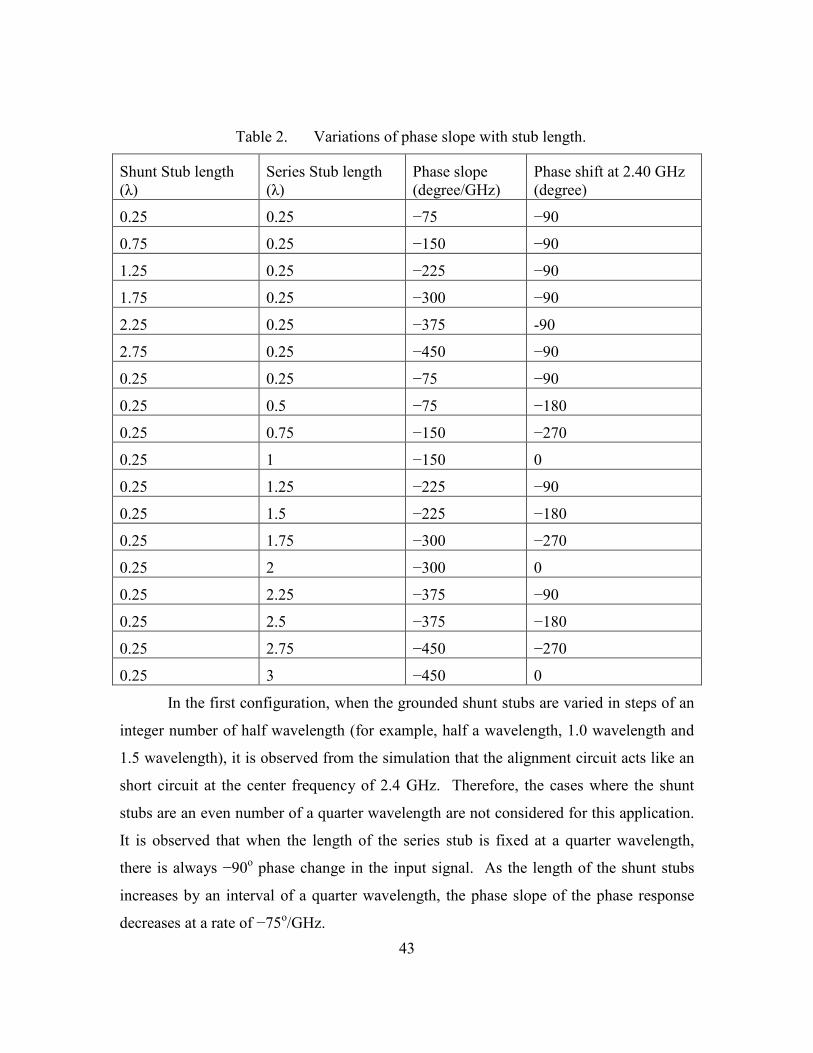
compensate the phase slope in the WLCC. The variation of phase slope with stub length
is shown in Table 2. Two basic configurations were simulated. In the first configuration,
the length of the series stub is fixed at quarter wavelength, and the shunt stubs are
increased in multiples of a quarter wavelength. In the second configuration, the length of
the shunt stubs are fixed at a quarter wavelength, and the length of the series stub is
increased in multiples of a quarter wavelength.
43
Table 2. Variations of phase slope with stub length.
Shunt Stub length (λ)
Series Stub length (λ)
Phase slope (degree/GHz)
Phase shift at 2.40 GHz (degree)
0.25 0.25 −75 −90
0.75 0.25 −150 −90
1.25 0.25 −225 −90
1.75 0.25 −300 −90
2.25 0.25 −375 -90
2.75 0.25 −450 −90
0.25 0.25 −75 −90
0.25 0.5 −75 −180
0.25 0.75 −150 −270
0.25 1 −150 0
0.25 1.25 −225 −90
0.25 1.5 −225 −180
0.25 1.75 −300 −270
0.25 2 −300 0
0.25 2.25 −375 −90
0.25 2.5 −375 −180
0.25 2.75 −450 −270
0.25 3 −450 0
In the first configuration, when the grounded shunt stubs are varied in steps of an
integer number of half wavelength (for example, half a wavelength, 1.0 wavelength and
1.5 wavelength), it is observed from the simulation that the alignment circuit acts like an
short circuit at the center frequency of 2.4 GHz. Therefore, the cases where the shunt
stubs are an even number of a quarter wavelength are not considered for this application.
It is observed that when the length of the series stub is fixed at a quarter wavelength,
there is always −90o phase change in the input signal. As the length of the shunt stubs
increases by an interval of a quarter wavelength, the phase slope of the phase response
decreases at a rate of −75o/GHz.

44
For a second configuration, where the length of the shunt stubs are fixed at a
quarter wavelength, the phase response of the circuit decreases by multiples of −90o
whenever there is an increase in the length of the series stub by a quarter wavelength. It
is also observed that the phase slope of the phase alignment circuit reduces at a rate of
−75o/GHz as the length of the series stub increases in intervals of a half a wavelength.
Based on previous simulations in Chapter II and Section B2 of this chapter, the
phase slope introduced by the non-ideal phase shifter and FDMC-based WLCC are
shown in Table 3.
Table 3. Phase slope introduced by various WLCC configurations.
Case LCC Design Phase slope
1 LCC with attenuator and non-ideal phase shifters −161.861o/GHz, or
−270o/frequency octave
2 FDMC with power splitters −452 radians/GHz, or
−25897.692o/GHz
3 FDMC with circulators −1650 radians/GHz, or
−94538.036o/GHz
In order to achieve zero phase shifts along the leakage path, the second
configuration is used, where the length of the shunt stubs is set to a quarter wavelength.
The length of the series stub is determined by using the case where the phase slope is the
closest to that of the LCC branch. For case one in Table 3 (non-ideal phase shifter), the
phase slope of the cancellation path is −161.861o/GHz; therefore, to achieve no phase
change in the leakage path with the matching path slope, the configuration with quarter
wavelength shunt stubs and 1.0 wavelength series stubs is used (in Table 2). For the case
where a FDMC with power splitters is used, the phase slope of the cancellation path is
−25897.692o/GHz, but it is also observed that the phase change at 2.4 GHz is −905.746o.
This makes it difficult to design a phase slope alignment circuit that has a phase change
of −905.746o at center frequency of 2.4 GHz. Similarly, for the case of FDMC where
circulators are used, there is a phase shift of −3427.794o at 2.4 GHz. The irregularities in
the phase slope curves of the FDMC designs can potentially reduce the effectiveness of

45
the phase slope alignment circuit. Therefore, in order to reduce the complexity and
maximize the effectiveness of the LCC design, the two FDMC designs are not considered
for further analysis. A summary of the length of the series stub required for the LCC
configuration is shown in Table 4. The corresponding phase slope of the phase alignment
circuit is also shown in Table 4.
Table 4. Length of shunt stubs for LCC design.
Wideband leakage cancellation circuit configuration
Length of series stub (wavelength)
Corresponding phase slope of phase alignment circuit (degree/GHz)
LCC with attenuator and non-ideal phase shifter
0.5 −150
When comparing data in Table 3 with that in Table 4, we find the errors in the
phase slopes between the cancellation and leakage paths to be 11.861o/GHz. The phase
slope alignment circuit is designed and applied on the leakage path in ADS. The results
and analysis are shown in the next section.
3. Application of Shunt Stub Circuit to the Leakage Path
As discussed in Section B3, the required length of the series stub is half a
wavelength, and the phase slope alignment circuit is applied on the leakage path as
shown in Figure 39. The simulation is carried out with source signal of frequency
ranging from 2.36 GHz to 2.44 GHz in steps of 1.0 MHz. The loss of the attenuator in
the LCC is swept from 0 to 25 dB in steps of 0.01 dB. The source power is set at 6.0
dBm, and an AC simulator with parameter sweep is used for this simulation.

46
Figure 39. Application of phase slope alignment circuit on LCC with non-ideal circulator.
The amplitude of the residual signal versus the attenuation in the cancellation path
is shown in Figure 40. It can be seen that the optimal LCC attenuation is about 19.32 dB.
It is also observed that the power of the residual signal ranges from −110.663 dB to
−64.748 dB for frequency band of interest. When compared to the results in Figure 24,
there is an improvement of about 10 to 15 dB in cancellation power at 2.4 GHz when the
phase slope alignment is applied to the leakage path. However, alignment error of
11.861o/GHz results in losses in the cancellation power at the boundary of the frequency
band of interest, 2.36 GHz and 2.44 GHz (Marker M1).

47
Figure 40. Plot of residual power versus LCC attenuation.
In order to further improve the performance of the cancellation circuit, a shunt
stub circuit is used in the cancellation circuit to replace the phase shifter as described in
the next section.

48
4. Application of Shunt Stub Circuit to the Cancellation and Leakage Paths
As discussed in Section C3, slight misalignment in the phase slope of the LCC
and leakage signal resulted in cancellation losses. In order to achieve coherent
cancellation of the leakage signal, the cancellation signal has to be of the same magnitude
and 180o out of phase when compared to the leakage signal. A shunt stub circuit can be
used to phase shift a signal and alter the change of phase over a range of frequencies, as
shown in Table 2. Therefore, in order to maintain 180o phase difference and common
phase slope between the cancellation signal and leakage signal, it is possible to select two
different sets of shunt stub circuits. The design of the LCC using stubs of transmission
lines in both paths is shown in Figure 41. The simulation is carried out with source signal
frequencies ranging from 2.36 GHz to 2.44 GHz in steps of 1.0 MHz. The loss of the
attenuator in the LCC is swept from 0 to 25 dB in steps of 0.01 dB. The source power is
set at 6.0 dBm, and an AC simulator with parameter sweep is used for this simulation.
Figure 41. Application of shunt stub circuits on both cancellation and leakage paths.

49
The shunt stubs with length of three quarter wavelength and series stub with
length of one quarter wavelength is applied on the cancellation path as part of the LCC
circuit (in Figure 41) and results in a −270o phase change at 2.4 GHz with a phase slope
of −150o/GHz. At the same time, the shunt stubs with length of one quarter wavelength
and a series stub with a length of three quarter wavelength are applied on the leakage path
as shown in Figure 41. The introduction of the stubs in the leakage path causes the
leakage signal to be phase shifted by −90o at 2.4 GHz with a phase slope of −150o/GHz.
The simulation is conducted with source frequency from 2.36 GHz to 2.44 GHz in steps
of 1.0 MHz. The LCC is tuned by sweeping the attenuator in the cancellation path from
0 dB to 25 dB in intervals of 0.01 dB. The variation of the residual signal with respect to
the LCC attenuation is shown in Figure 42.
Figure 42. Plot of residual power versus LCC attenuation with 2 sets of shunt stubs circuits.
As it is observed from Figure 42 that with better alignment of the phase slope
between the cancellation and leakage paths, the residual signal can be reduced by about

50
−110 dB. It is also observed that the deep notch of cancellation occurs when the
attenuation of the LCC is set to 20 dB. By setting the attenuation of the LCC at 20 dB,
the simulation is repeated for the purpose of amplitude and phase analysis. The phase of
the leakage and cancellation paths is shown in Figure 43.
Figure 43. Phase angles of the leakage and cancellation paths versus frequency.
100
50 <l> <l> ~
0> <l> 0 c 0 ·-<l> (/) cu ..c a..
-50
-100
-
-
m3 freq=2.390GHz phase(var("4_LCCOut"))=91 .499 phase(var("3 Stu bOut") )=-88. 501
m2 freq=2. 370GHz phase(var("4_LCC0ut"))=94.497 phase(var("3 StubOut"))=-85.495
m1 freq=2.400GHz phase(var("4_LCCOut"))=90.000 phase(var("3 StubOut"))=-90.000
m2 m3 m1 ~r ~, ~,
-
-
~ancellation
Leak1ge I
I I I I I I I I I I I I I ~ I I I I ~ I I I I I I I I I I I I I I I I I I
2 .36 2 .37 2.38 2.39 2.40 2.41 2.42 2.43 2.44
Frequency in GHz

51
As in Figure 43, the phase difference between the leakage and cancellation is
maintained at 180o in general (Markers M1 and M3). However, there are slight errors in
the phase difference between the two signals as can be observed in Marker M2 shown in
Figure 43.
The slight imbalance between the leakage and cancellation results in a non-
uniform magnitude response of the cancellation. The magnitude of the residual signal is
shown in Figure 44.
Figure 44. Magnitude of residual signal versus frequency.
It is observed from Figure 43 that the slight variations between the two paths
result in a difference of about 13 dB across the frequency band of interest. However, in
this case, the variation is more controlled when compared to the case shown in Figure 40
where the variation is approximately 55 dB.
The magnitude responses of the two shunt stub circuits are shown in Figure 45
and Figure 46 for amplitude imbalance analysis. As can be seen in Figure 45 and Figure

52
46, the difference between the magnitude response at 2.36 GHz and 2.44 GHz is 0.022
dB; this slight amplitude imbalance contributes to the variations of the residual signal
with frequency as shown in Figure 44. Such a small difference in the magnitude response
cannot be measured reliably.
With the amplitude and phase imbalance introduced by the pair of stubs circuits,
the cancellation power of the LCC is shown in Figure 47. It is observed in Figure 47 that
the peak cancellation occurs at about 2.38 GHz and 2.42 GHz with cancellation power of
about 87 dB. The 3.0 dB bandwidth of the cancellation circuit is about 56 MHz.
Figure 45. Magnitude responses of phase slope alignment circuits with three quarter wavelength shunt stubs and quarter wavelength series stubs applied to
leakage path.

53
Figure 46. Magnitude responses of WLCC with phase slope alignment circuits with quarter wavelength shunt stubs and three quarter wavelength series stub.
Figure 47. Cancellation C versus frequency.

54
5. Mismatch Effects of a Dipole Antenna
The analysis of WLCC performance so far has been carried out using a constant
real impedance. Such a termination circuit cannot truly represent the behavior of an
antenna, as the input impedance of the antenna such as a dipole has a reactive part that is
frequency dependent. Other characteristics of the antenna affect its VSWR and make it
frequency dependent, as it can be observed in Figure 48.
Figure 48. Calculated VSWR as a function of frequency for dipoles of different wire diameter (From [18]).
The bandwidth of a dipole antenna is usually narrow because of its resonant-type
structure [18]. Reflections from the dipole terminals are more serious when operating in
a wideband scenario. For the case of a thin dipole antenna, the length-to-diameter ratio is
about 50, and the input resistance is given by
2.4
24.7riLR πλ
=
(7)
where Rri is the input resistance, L is that length of dipole antenna and λ is the wavelength
at center frequency.
For the case where the center frequency is 2.40 GHz, the wavelength is found to
be 0.125 m. The length of the dipole is taken to be 0.475λ so that the antenna can be

55
made to resonate [18]. The input resistance of the dipole antenna is found to be 64.554
Ω. In order to match the impedance of the dipole antenna to that of the rest of the circuit,
a quarter-wave transformer is used [12].
The desired input impedance of the quarter-wavelength transformer is given by
1 0 riZ Z R= (8)
where, Z1 is the impedance of the quarter-wavelength transformer and Z0 is the
characteristic impedance of the feedline which is 50 Ω. The impedance of the quarter-
wavelength transformer is found to be 56.813 Ω.
The ADS model of the LCC with a dipole antenna is shown in Figure 49. The
attenuation of the LCC is set to 20 dB, and the simulation is carried out with source
frequency ranging from 2.36 GHz to 2.44 GHz in steps of 1.0 MHz. In the simulation,
the source power is set at 6.0 dBm. The result of the simulation is shown in Figure 50,
where the WLCC is set for a 50 Ω antenna impedance. In Figure 50, it is found that with
the introduction of a dipole antenna, the cancellation power is reduced by 55 to 75 dB.
Figure 49. ADS model of LCC with a dipole antenna.
CIR3 Port 2

56
Figure 50. Residual signal level with dipole antenna, LCC attenuation of 20 dB.
The attenuator in the LCC is tuned to obtain a minimum in the residual signal. It
was found through simulation that the residual signal is minimal when the attenuation is
set to 21.8 dB. The residual signal of the retuned circuit is shown in Figure 51.
It is observed that by retuning the LCC, the cancellation power is slightly
improved by about 25 dB at around the center frequency. In order to understand the
source of loss of cancellation power, the signal at Port 2 of the circulator CIR3 in Figure
49 is analyzed and shown in Figure 52.
It is observed in Figure 52 that the power of the signal along the antenna path is
dependent on operating frequency. This is because the dipole mismatch is frequency
dependent. This can give rise to both amplitude and phase imbalance between the
leakage and cancellation paths. This is because the reflected dipole signal is circulated
into the leakage path. The magnitude and phase of the leakage and cancellation path is
shown in Figure 53 and Figure 54, respectively.

57
Figure 51. Residual signal level with dipole antenna, LCC attenuation of 21.8 dB.
Figure 52. Signal level at the Port 2 of circulator along the antenna path.

58
Figure 53. Magnitude of the leakage and cancellation signals with source of 6.0 dBm.
Figure 54. Phase of the leakage and cancellation signals.

59
It is shown in Figure 53 that the magnitude of the leakage signal is different from
the cancellation signal for frequencies other than the center frequency of 2.40 GHz.
Therefore, with the amplitude imbalance between the leakage and cancellation signals,
the leakage signal is not cancelled completely.
In coherent cancellation, when the amplitude is balanced, the phase angle between
the leakage and cancellation signals is maintained at 180o. However, as shown in Figure
54, the phase difference between the two signals is not maintained at 180o. With the
magnitude and phase imbalance between the leakage and cancellation paths, the LCC is
not effective in handling frequency dependent reflection from a load antenna.
It should be pointed out that since the dipole is a narrowband device, there is no
need for a wideband LCC. A narrowband LCC will suffice. Techniques to increase the
antenna bandwidth are discussed in [19]. Broadbanding involves synthesizing a circuit to
match one impedance to another impedance over a specific frequency range to within a
specific tolerance. The impedance to be matched is a function of frequency that is
usually complex. It is recommended in [19] to adopt an iterative approach for
broadbanding. Discussion and analysis of broadbanding techniques are beyond the scope
of this thesis.
6. Application of Spiral Antenna
As was discussed in Section 5, the frequency response of a dipole antenna is
narrowband in general, and this affects the overall performance of the WLCC. In this
section, the performance of the WLCC when operating with a broadband spiral antenna is
investigated. For the purpose of this study, the reflectivity or S11 parameter of a spiral
antenna (in Table 5) is considered.
The magnitude and phase responses of the S11 parameter of the spiral antenna are
shown in Figure 55 and Figure 56, respectively. It can be observed in Figure 55 and
Figure 56 that the variations in the amplitude and phase of the S11 parameter of the spiral
antenna are frequency dependent.

60
Table 5. S11 parameters of spiral antenna used for simulation.
Frequency in GHz Magnitude of S11 Phase of S11 in degree 2.36 0.027134791 -1459.6083 2.3639996 0.013727983 -1396.1334 2.3759999 0.03184228 -1354.0186 2.388 0.055112332 -1353.222 2.3999996 0.077660158 -1359.1818 2.4119999 0.098555103 -1367.325 2.424 0.011720579 -1376.578 2.4359996 0.13300213 -1386.578 2.44 0.14528446 -1397.1576
The ADS model of the WLCC with the spiral antenna is shown in Figure 57. The
spiral antenna is modeled by a S1P (1-Port S-parameter File) in ADS using the S11
parameter as shown in Table 5. An AC simulator is used for the simulation in this
section. The simulation is carried at source power of 6.0 dBm and frequency from 2.36
GHz to 2.44 GHz in steps of 1.0 MHz. It should be noted that the attenuation of the
WLCC is set to 20 dB as it has been tuned for wideband application.
Figure 55. Magnitude of S11 parameter of spiral antenna with frequency.

61
Figure 56. Phase responses of the S11 parameter of spiral antenna with frequency.
Figure 57. ADS model of WLCC with spiral antenna.

62
The simulation settings for the spiral antenna model are shown in Figure 58. In
order to use ADS, the S11 parameter of the spiral antenna has to be formatted and stored
in a text file. The syntax of the S11 parameter text file is shown in Figure 59.
The magnitude of the residual signal is shown in Figure 60. It is observed that the
magnitude of the residual signal is very similar to the magnitude response of the S11
parameter of the spiral antenna (in Figure 55). This is because the leakage signal is
dominated by the reflection of the spiral antenna in this case.
Figure 58. ADS simulation setting for the spiral antenna model.

63
! Frequency / GHz S1,1/abs,linear S1,1/arg,degrees !----------------------------------------------------------------------- # GHZ S MA R 50 ! freq magS11 angS11 (commented header line) 2.36 0.027134791 -1459.6083 2.3639996 0.013727983 -1396.1334 2.3759999 0.03184228 -1354.0186 2.388 0.055112332 -1353.222 2.3999996 0.077660158 -1359.1818 2.4119999 0.098555103 -1367.325 2.424 0.11720579 -1376.578 2.4359996 0.13300213 -1386.578 2.44 0.14528446 -1397.1576
Figure 59. Syntax of spiral antenna S11 parameter file.
Figure 60. Magnitude of residual signal in dBm with frequency at source power of 6.0 dBm.

64
The magnitude and phase of the WLCC output and the leakage signal are shown
in Figure 61 and Figure 62, respectively. It is observed that there are both amplitude and
phase imbalances between the cancellation and leakage signals. As a result, there is
always some substantial leakage power as shown in Figure 60. It is also observed that
the amplitude and phase differences between the cancellation and leakage signals vary
with frequency.
Figure 61. Magnitude of the cancellation and leakage signals.
From Figure 61 and Figure 62, it is observed that at the center frequency of 2.4
GHz there are amplitude and phase difference of 3.088 dBm and 139.222o. In order to
fine tune the difference between the cancellation and leakage signal, the amplitude and

65
phase of the cancellation signal are adjusted. An additional phase shifter is added along
the cancellation path to introduce the phase lag in the cancellation signal (in Figure 63).
The simulation is conducted with a 6.0 dBm source and source frequency from 2.36 GHz
to 2.44 GHz with steps of 1.0 MHz.
Figure 62. Phase of cancellation and leakage signals.

66
Figure 63. ADS model of modified WLCC with spiral antenna.
The phase shifter (PS1) and the attenuator (ATTEN1) are tuned such that the
cancellation and leakage signals are of same amplitude and 180o out of phase as shown in
Figure 64 and Figure 65. It is observed from Figure 64 and Figure 65 that coherent
cancellation occurs only at the center frequency, and beyond that there are losses in the
cancellation power.
In Figure 66, the amplitude of the residual power is shown. It is observed from
Figure 66 that the cancellation is narrowband with a notch at about −61 dBm. The
WLCC design with grounded shunt stubs is ineffective in reducing the leakage signal
over the entire frequency band in this case.
PS1
ATTEN1

67
Figure 64. Magnitude of cancellation and leakage signal with frequency at source power of 6.0 dBm.
Figure 65. Phase of the cancellation and leakage signals with frequency.

68
Figure 66. Magnitude of residual signal with frequency.
The reflections from the spiral antenna vary with frequency in a non-linear
manner. However, the WLCC is designed to cancel leakage signal that has a similar
characteristics of the source signal. The WLCC is able to cancel the linear phase slope in
the leakage signal but not non-linear phase slopes. For this reasons, there is a reduction
in cancellation when operating over a wideband.
D. SUMMARY
In this chapter, it was shown that the cancellation of the FDMC WLCC is not
optimal as the design introduced both amplitude and phase imbalance. It was shown
there is a negative phase slope that is associated with the phase response of the FDMC
LCC.
A phase slope alignment circuit that consists of both shunt and series stubs is used
to compensate the frequency dependent phase shift characteristics of the WLCC. In order

69
to keep the design of the LCC simple, the FDMC with phase slope alignment circuit was
not considered. In general, the phase characteristics of the phase slope alignment circuit
are discrete; for example, phase slope decreases in steps of 75o/GHz with an increase in
the length of the shunt stub by a quarter wavelength. This characteristic limits the tuning
of stub circuit to perfectly match the phase slope of a phase shifter in a LCC design. The
phase mismatch results in losses in the cancellation power. In order to achieve coherent
cancellation of the leakage signal, stub circuits were applied in both cancellation and
leakage paths.
Dipole antennas are narrowband and introduce both amplitude and phase
imbalance when operating beyond the center frequency. This results in loss in the
cancellation power. Techniques that match the antenna impedance to the characteristic
impedance of the feedline over a wideband should be investigated.
In general, the magnitude response of the WLCC is frequency independent and
phase response varies linearly with frequency. The performance of the WLCC degrades
for situation where the reflection from a load antenna varies with frequency non-linearly.

70
THIS PAGE INTENTIONALLY LEFT BLANK

71
IV. SUMMARY, CONCLUSIONS, AND RECOMMENDATIONS
A. SUMMARY
The aim of this research was to improve the cancellation performance of a
WLCC. The approach of the research was to investigate LCC techniques in the analog
domain. ADS was used to model and simulate characteristic of various LCC
configurations for analysis purposes.
One of the ways to isolate transmit and receive signals in a simultaneous transmit
and receive radar is with a circulator. Typical isolation of a circulator is about 20 to 30
dB between the three ports of the device. As a result of this imperfect isolation, leakage
of the transmit signal into the receive path occurs. The problem with transmit signal
leakage into the receive path is that the strong leakage tends to overwhelm the power
detector in the receive path and degrade the receiver’s sensitivity.
The idea of a leakage cancellation circuit is to coherently subtract the leakage
signal using transmit signal itself. The transmit signal was attenuated and phase shifted
so that an equal but 180o out-of-phase cancellation signal was produced to cancel the
leakage signal. However, hardware components do not behave ideally, and this results in
losses in the cancellation. When non-ideal devices are used, it was found that the
residual signal can be minimized by retuning the attenuator in the cancellation path.
Non-ideal frequency dependent phase response of the phase shifter narrows the
bandwidth of the cancellation circuit. This restricted the application of the LCC in
wideband cancellation.
The concept of the FDMC based WLCC was to divide the signals into multiple
frequency sub-bands, and subsequently, a narrowband LCC was applied on each
frequency sub-band. Elliptic band-pass filters were applied in the design of the FDMC
WLCC. As both the magnitude and phase responses of the FDMC WLCC were
frequency dependent, coherent cancellation could not be achieved. This was because of
the amplitude and phase imbalance between the cancellation and leakage signals.

72
The use of shunt and series stubs of transmission lines could be used to design
phase alignment circuit. By applying the phase slope alignment circuit on a non-ideal
phase shifter, higher cancellation can be achieved if the rate of phase change with
frequency of phase slope alignment circuit matches that of the phase shifter. The phase
alignment circuit changed in steps of −90o and −75o/GHz. As a result, it was impossible
to tune the phase alignment circuit such that its phase slope matched exactly that of the
phase shifter.
The idea of using a pair of phase slope alignment circuits was studied in this
thesis. Phase slope cancellation circuits were employed on both cancellation and leakage
paths to maintain amplitude and phase balance between the two signals. It was found that
this configuration could greatly improve the performance of the LCC by reducing the
residual signal below −110 dB.
The WLCC has its limitation in cancelling leakage signals that vary with
frequency non-linearly. Techniques that control the reflections from the antenna load
should be further studied.
B. CONCLUSIONS
In conclusion, the LCC can be applied to provide isolation between the transmit
and receive paths of simultaneous transmit and receive systems. Detailed design is
required in the building of the LCC to ensure amplitude and phase balance between the
cancellation and leakage signals.
Accurate modeling of LCC components such as the phase shifter provides better
understanding of bandwidth and cancellation limitation of the LCC. This has helped to
fine tune LCC design concepts developed in earlier research. The main contributions of
this thesis are the analysis of the LCC designs presented in earlier thesis research,
analysis of grounded shunt stub circuits and the use of shunt stub based phase slope
alignment circuits to improve LCC cancellation performance. The maximum
cancellation of a stub circuit based LCC is about 87 dB. The three dB bandwidth of the
cancellation is about 56 MHz.

73
C. RECOMMENDATIONS
1. Broadbanding Techniques for Antenna Impedance Matching
The impedance of the antenna can be frequency dependent as presented in
Chapter III, and this resulted in loss in cancellation. Broadbanding can be a possible
technique used to match the antenna impedance over a wider frequency range of interest.
This helps to reduce the reflection from the antenna and, hence, reduce leakage from the
transmit path. An ADS model of a matching circuit can be created for the study of
broadbanding.
2. Modeling of Transmit and Receive Module
As was seen in this thesis, coherent cancellation of a leakage signal is sensitive to
amplitude and phase imbalance. Transmit and receive modules (TRMs) used in a
WNDDPA may introduce reflections that can affect the LCC by introducing amplitude
and phase imbalance between cancellation and leakage paths. An ADS model can be
built to investigate the effects of the TRM on the LCC.
3. Modeling with ADS Transient Simulator
The modeling of the WLCC was carried out using ADS AC Simulator and the
steady state results were presented. The simulation model can be extended to study the
transient performance of the WLCC using the ADS transient simulator. This can help to
understand the impact of a fast changing source signal and various waveform
modulations.
4. Hardware Prototype
With the understanding of the reflections from the antenna and TRM and the
ways to minimize their impacts on the LCC, a hardware prototype can be fabricated for
the transmit signal and receive signal isolation in WNDDPA. The hardware prototype of
the WLCC can be used for further study of the related field for future field
implementation of a WNDDPA.

74
THIS PAGE INTENTIONALLY LEFT BLANK
75
LIST OF REFERENCES
[1] Jane’s Information Group, Airborne radar systems, http://search.janes.com.libproxy.nps.edu/Search/documentView.do?docId=/content1/janesdata/yb/jav/jav_9788.htm@current&pageSelected=allJanes&keyword=FMCW%20radar&backPath=http://search.janes.com/Search&Prod_Name=JAV&, accessed on 22 Oct 2011.
[2] K. L. Fuller, “To see and not to be seen,” Radar and Signal Processing, IEEE Proceedings F, vol. 137, pp 1–10, Issue 1, 1990.
[3] M. I. Skolnik, Introduction to Radar Systems, 2nd Edition, McGraw-Hill, 1980.
[4] A. Moussa, Y. Khalaf and A. Khalil, “Design of a novel circulator for wireless transceivers,” International Conference on Microelectronics, pp267–270, December 2007.
[5] S. D. Andrenko, I. A. Vyazmitinov and Y. B. Sidorenko, “An antenna system of a continuous wave radar,” 4th International Conference on Antenna Theory and Techniques, pp 300–303, September 2003.
[6] Qi Jiming, Qu Xinjian and Ren Zhijiu, “Development of A 3cm Band Reflected Power Canceller,” in Proceedings of International Conference on Radar, pp1098–1102, October 2001.
[7] Jun Zhang and Xu Zhou, “Investigation on adaptive leakage nulling for Pseudo-random code CW radar,” IET International Radar Conference, pp 1–4, April 2009.
[8] T. Venkatamuni, L. S. Sudhakara Sarma, A. T. Kalghatgi, “Adaptive reflected power canceller for single antenna FMCW radar,” Asia Pacific Microwave Conference, pp 1841–1844, 2009.
[9] Wei-Han Cheng, “Cancellation circuit for transmit-receive isolation,” Naval Postgraduate School Master’s Thesis, September 2010.
[10] D. C. Jenn, Ji Heon Ryu and R. Broadston, “Adaptive Phase Synchronization in Distributed Digital Arrays,” Conference on Adaptive Hardware and Systems, pp 199–204, June 2010.
[11] T. H. Ang, “Conceptual design and software simulation of a wideband leakage cancellation circuit,” Naval Postgraduate School Master’s Thesis, December 2010.
[12] David M. Pozar, Microwave Engineering, 3rd ed, John Wiley & Sons, 2005.

76
[13] Pasternack SMA Female Power Divider PE2014; 2–4 GHz Data sheet, Pasternack Enterprises, Irvine, CA, Rev A.
[14] Spectrum Microwave 6708 phase shifter Data sheet, Spectrum Microwave, Hudson, NH.
[15] R. W. Burns, R. L. Holden and R. Tang, “Low cost Design Techniques for Semiconductor Phase Shifters,” IEEE Transactions on Microwave Theory and Techniques, vol. MTT-22, pp 675–688, No. 6, June 1974.
[16] Soon-Young Eom, “Broadband 180o Bit Phase Shifter Using a λ/2 Coupled Line and Parallel λ Stubs,” IEEE Microwave and Wireless Components Letters, vol. 14, pp 228–230, No. 5, May 2004.
[17] Xinyi Tang and Koen Mouthaan, “Phase-Shifter Design Using Phase-Slope Alignment With Grounded Shunt λ/4 Stubs,” IEEE Transactions on Microwave Theory and Techniques, vol. 58, pp 1573–1583, No. 6, June 2010.
[18] Warren L. Stutzman and Gary A, Thiele, Antenna Theory and Design, 2nd Edition, John Wiley & Sons, 1998.
[19] Richard C. Johnson and Henry Jasik, Antenna Engineering Handbook, 2nd Edition, McGraw Hill, ch. 43, 1984.

77
INITIAL DISTRIBUTION LIST
1. Defense Technical Information Center Ft. Belvoir, Virginia
2. Dudley Knox Library Naval Postgraduate School Monterey, California
3. Professor R. Clark Robertson Chairman, Department of Electrical & Computer Engineering Naval Postgraduate School Monterey, California
4. Professor David C. Jenn Professor, Department of Electrical & Computer Engineering Naval Postgraduate School Monterey, California
5. Professor Ric Romero Assistant Professor, Department of Electrical & Computer Engineering Monterey, California
6. Professor Tat Soon Yeo Director, Temasek Defence Systems Institude (TDSI) Nation University of Singapore Singapore
7. Ms Lai Poh Tan Senior Manager, Temasek Defence Systems Institude (TDSI) National University of Singapore Singapore
8. Mr Pek Wee Kok Singapore Technologies Dynamics Pte Ltd Singapore