Embed Size (px)
Citation preview

NAU8810
emPowerAudio™ Datasheet Revision 2.7 Page 1 of 100 June 2016
Differential/Mono Audio Codec with 2-wire Interface Control Interface
emPowerAudio™ 1. GENERAL DESCRIPTION
The NAU88U10 is a cost effective low power wideband Monophonic audio CODEC. It is suitable for a wide range
of audio applications, including voice telephony. Supported functions include a 5-band Graphic Equalizer,
Automatic Level Control (ALC) with noise gate, PGA, standard I2S or PCM audio interface, optional PCM time
slot assignment, and a full fractional-N on-chip PLL. This device includes one differential microphone input, and
multiple variable gain control stages in the audio paths. Both a Mono headset/line-level output and a high power
differential BTL speaker driver output are provided.
The analog input path includes a PGA enabling dynamic range optimization of a wide range of input sources with
programmable gain from -12dB to +35.25dB. In addition to a digital high pass filter to remove DC offset voltages,
the ADC also features programmable voice band digital filtering. Audio data is communicated via the audio
interface that supports multiple I2S and PCM data formats. The DAC converter path includes filtering, and mixing,
programmable-gain amplifiers, and soft muting. The 2-Wire digital control interface has an independent supply
voltage to enable easy integration into multiple supply voltage systems. The NAU88U10 operates at supply
voltages from 2.5V to 3.6V, and the digital core can operate at a voltage as low as 1.71V to conserve power.
The NAU88U10 is specified for operation from -40C to +85C, and is automotive AEC-Q100 grade qualified.
2. FEATURES
24-bit signal processing linear Audio CODEC
Audio DAC: 93dB SNR and -84dB THD Audio ADC: 91dB SNR and -79dB THD Support variable sample rates from 8 - 48kHz Analog I/O
Integrated programmable Microphone Amplifier Integrated BTL Speaker Driver 1 W (8Ω / 5V) Earphone / Speaker / Line-Output Mixing / Routing Integrated Headset Driver 40mW (16Ω / 3.3V) Low Noise bias supply voltage for microphone On-chip full fractional-N PLL Interfaces
I2S digital interface PCM time slot assignment
2-Wire serial control Interface (I2C style; /Write capable)

NAU8810
emPowerAudio™ Datasheet Revision 2.7 Page 2 of 100 June 2016
Low Power, Low Voltage
Analog Supply: 2.5V to 3.6V Digital Supply: 1.71V to 3.6V Nominal Operating Voltage: 3.3V Additional features
5-band Graphic Equalizer Programmable ALC ADC Notch Filter Programmable High Pass Filter Digital ADC/DAC Passthrough Mono data output on both channels Automotive AEC-Q100 grade 3 & TS16949 qualification, tested to a higher reliability standard
Temperature: –40C to +85C Applications
All types of wired/wireless telephony Security Systems Mobile Telephone Hands-free Kits Residential & Consumer Intercoms
Digital Audio Interface Control IF
Microphone
Interface
Output
MixersADC DAC
-1
Input
Mixers &
Gain
Stage
I2S PCM 2-wire
MIC-
MIC+
Digital I/OAudio I/O
ADC Filter
Volume
Control
HPF
Notch
Filter
DAC Filter
Volume
Control
Limiter
SPKOUT-
SPKOUT+
MOUT
Microphone
BiasMICBIAS
3. PIN CONFIGURATION
MIC
-
VSSSPK
MC
LK
VDDA
VDDD
SP
KO
UT
-
SPKOUT+
MOUT
DA
CIN FS
BC
LK
VSSA
VSSD
AD
CO
UT
VD
DS
PK
SDIO
VR
EF
2
3
4
5
6 7 8
1
10
15
14
13
12
11
16
9
20
19
18
17
SCLK
Metal
Paddle
(VSSA)
MIC
+
MICBIAS
Figure 1: 20-Pin QFN Package

NAU8810
emPowerAudio™ Datasheet Revision 2.7 Page 3 of 100 June 2016
4. PIN DESCRIPTION
Pin Name 24-Pin Functionality A/D Pin Type
MICBIAS 1 Microphone Bias A O
VDDA 2 Analog Supply A I
VSSA 3 Analog Ground A O
VDDD 4 Digital Supply D I
VSSD 5 Digital Ground D O
ADCOUT 6 Digital Audio Data Output D O
DACIN 7 Digital Audio Data Input D I
FS 8 Frame Sync D I/O
BCLK 9 Bit Clock D I/O
MCLK 10 Master Clock D I
SCLK 11 2-Wire Serial Clock D I
SDIO 12 2-Wire I/O D O
MOUT 13 MONO Output A O
SPKOUT+ 14 Speaker Positive Output A O
VSSSPK 15 Speaker Ground A O
SPKOUT- 16 Speaker Negative Output A O
VDDSPK 17 Speaker Supply A I
VREF 18 Decoupling internal analog mid supply reference
voltage
A O
MIC- 19 Microphone Negative Input A I
MIC+ 20 Microphone Positive Input A I
Table 1: Pin Description
Notes
1. The 20-QFN package includes a bulk ground connection pad on the underside of the chip. This bulk ground
should be thermally tied to the PCB, and electrically tied to the analog ground.
2. Unused analog input pins should be left as no-connection.
3. Any unused digital input pin must be tied high or low as appropriate.
NAU8810
emPowerAudio™ Datasheet Revision 2.7 Page 4 of 100 June 2016
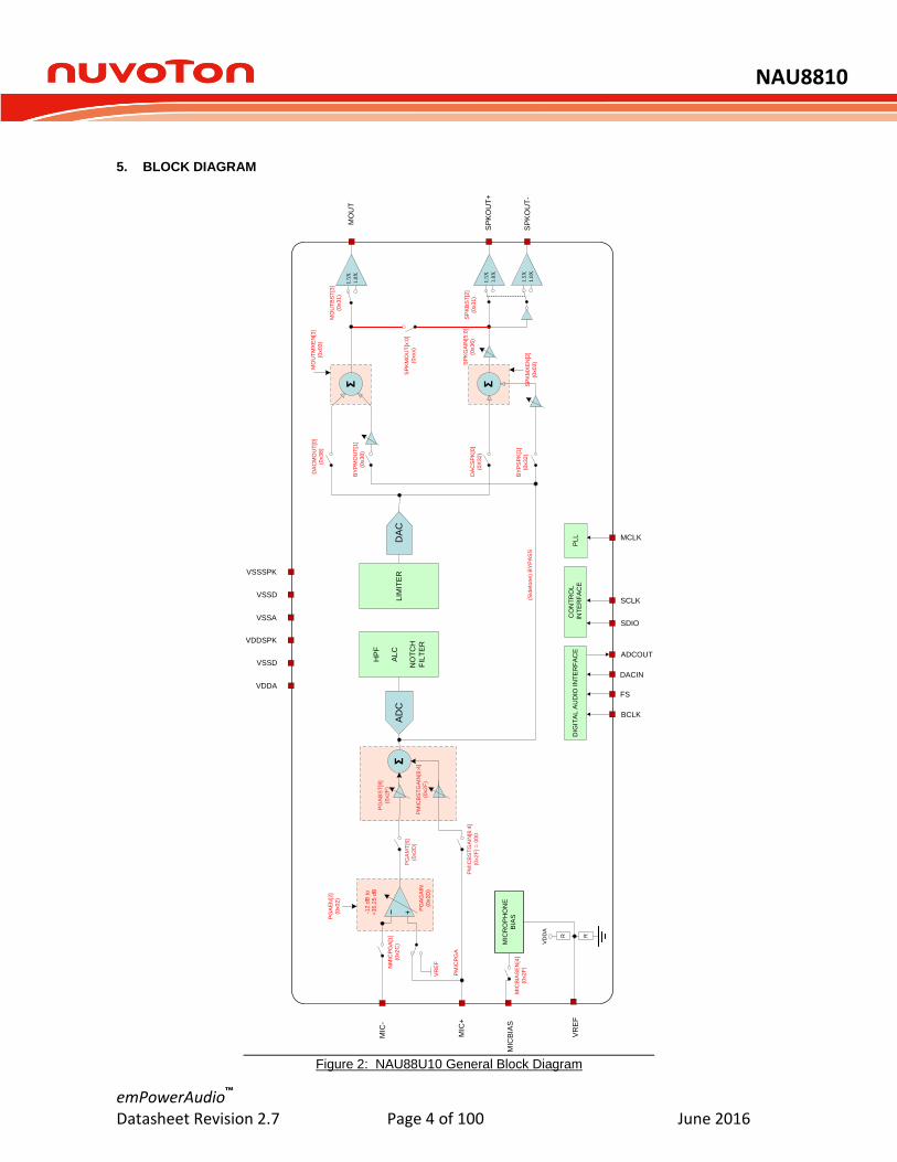
5. BLOCK DIAGRAM
Figure 2: NAU88U10 General Block Diagram
HP
F
AL
C
NO
TC
H
FIL
TE
R
LIM
ITE
R
(S
ide
ton
e)
BY
PA
SS
AD
CD
AC
VSSD
VDDA
VSSA
VDDSPK
VSSD
VSSSPK
BCLK
CO
NT
RO
L
IN
TE
RF
AC
E
DACIN
ADCOUT
FS
DIG
ITA
L A
UD
IO IN
TE
RF
AC
E
SCLK
SDIO
PM
ICB
ST
GA
IN[6
:4]
(0x2
F)
= 0
00
PG
AM
T[6
]
(0x2
D)
PM
ICB
ST
GA
IN[6
:4]
(0x2
F)
PG
AB
ST
[8]
(0x2
F)
Σ
MIC
+
MIC
-N
MIC
PG
A[1
]
(0x2
C)
PM
ICP
GA
VR
EF
PG
AG
AIN
(0x2
D)
-12
dB
to
+3
5.2
5 d
B
PG
AE
N[2
]
(0x0
2)
MO
UT
SP
KO
UT
+
SP
KO
UT
-
MO
UT
MX
EN
[3]
(0x0
3)
SP
KG
AIN
[5:0
]
(0x3
6)
DA
CS
PK
[0]
(0X
32)
DA
CM
OU
T[0
]
(0x3
8)
SP
KM
XE
N[2
]
(0x0
3)
BY
PM
OU
T[1
]
(0x3
8)
BY
PS
PK
[1]
(0x3
2)
SP
KB
ST
[2]
(0x3
1)
MO
UT
BS
T[3
]
(0x3
1)
ΣΣ1
.0X
1.5
X
1.0
X
1.5
X
1.0
X
1.5
X
SP
KM
OU
T[x
:0]
(0xxx)
MCLK
VR
EF
MIC
BIA
S
PL
L
RR
MIC
RO
PH
ON
E
BIA
S
VD
DA
MIC
BIA
SE
N[4
]
(0x2
F)

NAU8810
emPowerAudio™ Datasheet Revision 2.7 Page 5 of 100 June 2016
6. Table of Contents
1. GENERAL DESCRIPTION .................................................................................................................................1 2. FEATURES .........................................................................................................................................................1 3. PIN CONFIGURATION .......................................................................................................................................2 4. PIN DESCRIPTION .............................................................................................................................................3 5. BLOCK DIAGRAM ..............................................................................................................................................4 6. TABLE OF CONTENTS ......................................................................................................................................5 7. LIST OF FIGURES ..............................................................................................................................................8 8. LIST OF TABLES ............................................................................................................................................. 10 9. ABSOLUTE MAXIMUM RATINGS ................................................................................................................... 11 10. OPERATING CONDITIONS .............................................................................................................................. 11 11. ELECTRICAL CHARACTERISTICS ................................................................................................................. 12 12. FUNCTIONAL DESCRIPTION .......................................................................................................................... 15
12.1. INPUT PATH .............................................................................................................................................. 15 12.1.1. The differential microphone input (MIC- & MIC+ pins) ................................................................... 15
12.1.1.1. Positive Microphone Input (MIC+) ........................................................................................... 16
12.1.1.2. Negative Microphone Input (MIC-) ........................................................................................... 17
12.1.1.3. PGA Gain Control ..................................................................................................................... 17 12.1.2. PGA Boost / Mixer Stage .................................................................................................................. 18
12.2. MICROPHONE BIASING ........................................................................................................................... 19 12.3. ADC DIGITAL FILTER BLOCK ................................................................................................................. 20
12.3.1. Programmable High Pass Filter (HPF)............................................................................................. 21 12.3.2. Programmable Notch Filter (NF) ...................................................................................................... 22 12.3.3. Digital ADC Gain Control .................................................................................................................. 22
12.4. PROGRAMMABLE GAIN AMPLIFIER (PGA) ........................................................................................... 23 12.4.1. Automatic level control (ALC) .......................................................................................................... 23
12.4.1.1. Normal Mode ............................................................................................................................. 26
12.4.1.2. ALC Hold Time (Normal mode Only) ....................................................................................... 26 12.4.2. Peak Limiter Mode ............................................................................................................................ 27 12.4.3. Attack Time ........................................................................................................................................ 28 12.4.4. Decay Times ...................................................................................................................................... 28 12.4.5. Noise gate (normal mode only) ........................................................................................................ 28 12.4.6. Zero Crossing .................................................................................................................................... 29
12.5. DAC DIGITAL FILTER BLOCK ................................................................................................................. 30 12.5.4. Hi-Fi DAC De-Emphasis and Gain Control ...................................................................................... 32 12.5.5. Digital DAC Output Peak Limiter ..................................................................................................... 32 12.5.6. Volume Boost .................................................................................................................................... 32 12.5.7. 5-Band Equalizer ............................................................................................................................... 33
12.6. ANALOG OUTPUTS .................................................................................................................................. 34 12.6.1. Speaker Mixer Outputs ..................................................................................................................... 34 12.6.2. Mono Mixer Output........................................................................................................................... 35 12.6.3. Differential Output Configuration .................................................................................................... 36 12.6.4. Unused Analog I/O ............................................................................................................................ 36
12.7. GENERAL PURPOSE CONTROL ............................................................................................................. 39 12.7.1. Slow Timer Clock .............................................................................................................................. 39

NAU8810
emPowerAudio™ Datasheet Revision 2.7 Page 6 of 100 June 2016
12.8. CLOCK GENERATION BLOCK ................................................................................................................ 39 12.9. CONTROL INTERFACE ............................................................................................................................ 43
12.9.1. 2-WIRE Serial Control (I2C Style Interface) ..................................................................................... 43
12.9.1.1. 2-WIRE Protocol Convention ................................................................................................... 43
12.9.1.2. 2-WIRE Write Operation ........................................................................................................... 44
12.9.1.3. 2-WIRE Operation .................................................................................................................... 44 12.10. DIGITAL AUDIO INTERFACES ................................................................................................................. 45
12.10.1. Right Justified audio data ................................................................................................................ 46 12.10.2. Left Justified audio data ................................................................................................................... 47 12.10.3. I
2S audio data .................................................................................................................................... 48
12.10.4. PCM audio data ................................................................................................................................. 49 12.10.5. PCM Time Slot audio data ................................................................................................................ 50 12.10.6. Companding ...................................................................................................................................... 51
12.11. POWER SUPPLY ...................................................................................................................................... 52 12.11.1. Power-On Reset ................................................................................................................................ 52 12.11.2. Power Related Software Considerations ........................................................................................ 52 12.11.3. Software Reset .................................................................................................................................. 53 12.11.4. Power Up/Down Sequencing ............................................................................................................ 53 12.11.5. Reference Impedance (REFIMP) and Analog Bias ......................................................................... 55 12.11.6. Power Saving ..................................................................................................................................... 55 12.11.7. Estimated Supply Currents .............................................................................................................. 55
13. REGISTER DESCRIPTION ............................................................................................................................... 57 13.1. SOFTWARE RESET .................................................................................................................................. 59 13.2. POWER MANAGEMENT REGISTERS ..................................................................................................... 59
13.2.1. Power Management 1........................................................................................................................ 59 13.2.2. Power Management 2........................................................................................................................ 60 13.2.3. Power Management 3........................................................................................................................ 60
13.3. AUDIO CONTROL REGISTERS ............................................................................................................... 60 13.3.1. Audio Interface Control .................................................................................................................... 60 13.3.2. Audio Interface Companding Control .............................................................................................. 61 13.3.3. Clock Control Register ..................................................................................................................... 62 13.3.4. Audio Sample Rate Control Register............................................................................................... 63 13.3.5. DAC Control Register ....................................................................................................................... 63 13.3.6. DAC Gain Control Register .............................................................................................................. 64 13.3.7. ADC Control Register ....................................................................................................................... 64 13.3.8. ADC Gain Control Register .............................................................................................................. 65
13.4. 5-BAND EQUALIZER CONTROL REGISTERS ........................................................................................ 66 13.5. DIGITAL TO ANALOG CONVERTER (DAC) LIMITER REGISTERS ....................................................... 67 13.6. NOTCH FILTER REGISTERS ................................................................................................................... 68 13.7. AUTOMATIC LEVEL CONTROL REGISTER ........................................................................................... 69
13.7.1. ALC1 REGISTER ............................................................................................................................... 69 13.7.2. ALC2 REGISTER ............................................................................................................................... 70 13.7.3. ALC3 REGISTER ............................................................................................................................... 71
13.8. NOISE GAIN CONTROL REGISTER ........................................................................................................ 72 13.9. PHASE LOCK LOOP (PLL) REGISTERS ................................................................................................. 73
13.9.1. PLL Control Registers ...................................................................................................................... 73 13.9.2. Phase Lock Loop Control (PLL) Registers ..................................................................................... 73
13.10. INPUT, OUTPUT, AND MIXERS CONTROL REGISTER.......................................................................... 74

NAU8810
emPowerAudio™ Datasheet Revision 2.7 Page 7 of 100 June 2016
13.10.1. Attenuation Control Register ........................................................................................................... 74 13.10.2. Input Signal Control Register ........................................................................................................... 74 13.10.3. PGA Gain Control Register .............................................................................................................. 75 13.10.4. ADC Boost Control Registers .......................................................................................................... 76 13.10.5. Output Register ................................................................................................................................. 76 13.10.6. Speaker Mixer Control Register ....................................................................................................... 77 13.10.7. Speaker Gain Control Register ........................................................................................................ 77 13.10.8. MONO Mixer Control Register .......................................................................................................... 78 13.10.9. Power Management 4........................................................................................................................ 78
13.11. PCM TIME SLOT CONTROL & ADCOUT IMPEDANCE OPTION CONTROL ......................................... 79 13.11.1. PCM1 TIMESLOT CONTROL REGISTER ......................................................................................... 79 13.11.2. PCM2 TIMESLOT CONTROL REGISTER ......................................................................................... 79
13.12. REGISTER ID ............................................................................................................................................ 80 13.12.1. Device revision register .................................................................................................................... 80 13.12.2. 2-WIRE ID Register ............................................................................................................................ 80 13.12.3. Additional ID ...................................................................................................................................... 80
13.13. Reserved ................................................................................................................................................... 80 13.14. OUTPUT Driver Control Register ............................................................................................................ 81 13.15. AUTOMATIC LEVEL CONTROL ENHANCED REGISTER ...................................................................... 82
13.15.1. ALC1 Enhanced Register ................................................................................................................. 82 13.15.2. ALC Enhanced 2 Register ................................................................................................................ 82
13.16. MISC CONTROL REGISTER .................................................................................................................... 83 13.17. Output Tie-Off REGISTER ........................................................................................................................ 84 13.18. AGC PEAK-TO-PEAK OUT REGISTER ................................................................................................... 84 13.19. AGC PEAK OUT REGISTER ..................................................................................................................... 84 13.20. AUTOMUTE CONTROL AND STATUS REGISTER ................................................................................ 85 13.21. Output Tie-off Direct Manual Control REGISTER .................................................................................. 85
14. CONTROL INTERFACE TIMING DIAGRAM .................................................................................................... 86 14.1. 2-WIRE TIMING DIAGRAM........................................................................................................................ 86
15. AUDIO INTERFACE TIMING DIAGRAM .......................................................................................................... 87 15.1. AUDIO INTERFACE IN SLAVE MODE ...................................................................................................... 87 15.2. AUDIO INTERFACE IN MASTER MODE................................................................................................... 87 15.3. PCM AUDIO INTERFACE IN SLAVE MODE (PCM Audo Data) ................................................................ 88 15.4. PCM AUDIO INTERFACE IN MASTER MODE (PCM Audo Data) ............................................................ 88 15.5. PCM AUDIO INTERFACE IN SLAVE MODE (PCM Time Slot Mode ) ....................................................... 89 89 15.6. PCM AUDIO INTERFACE IN MASTER MODE (PCM Time Slot Mode ) ................................................... 89 15.7. System Clock (MCLK) Timing Diagram ...................................................................................................... 90 15.8. µ-LAW ENCODE DECODE CHARACTERISTICS .................................................................................... 91 15.9. A-LAW ENCODE DECODE CHARACTERISTICS .................................................................................... 92 15.10. µ-LAW / A-LAW CODES FOR ZERO AND FULL SCALE ........................................................................ 93 15.11. µ-LAW / A-LAW OUTPUT CODES (DIGITAL MW) ................................................................................... 93
16. DIGITAL FILTER CHARACTERISTICS ........................................................................................................... 94 17. TYPICAL APPLICATION .................................................................................................................................. 96 18. PACKAGE SPECIFICATION ............................................................................................................................ 97 19. ORDERING INFORMATION ............................................................................................................................. 98 20. VERSION HISTORY ......................................................................................................................................... 99

NAU8810
emPowerAudio™ Datasheet Revision 2.7 Page 8 of 100 June 2016
7. List of Figures
Figure 1: 20-Pin QFN Package .....................................................................................................................................2
Figure 2: NAU88U10 General Block Diagram ...............................................................................................................4
Figure 3: Input PGA Circuit Block Diagram ................................................................................................................. 16
Figure 4: Boost Stage Block Diagram ......................................................................................................................... 18
Figure 5: Microphone Bias Schematic ......................................................................................................................... 19
Figure 6: ADC Digital Filter Path Block Diagram ......................................................................................................... 20
Figure 7: ALC Block Diagram ...................................................................................................................................... 23
Figure 8: ALC Response Graph .................................................................................................................................. 24
Figure 9: ALC Normal Mode Operation ....................................................................................................................... 26
Figure 10: ALC Hold Time ........................................................................................................................................... 27
Figure 11: ALC Limiter Mode Operations .................................................................................................................... 27
Figure 12: ALC Operation with Noise Gate disabled ................................................................................................... 28
Figure 13: ALC Operation with Noise Gate Enabled ................................................................................................... 29
Figure 14: DAC Digital Filter Path ............................................................................................................................... 30
Figure 15: DAC Digital Limiter Control ........................................................................................................................ 32
Figure 16: Speaker and MONO Analogue Outputs [To Update ? output from Auxilliary Amplifier] ............................. 34
Figure 17: Tie-off Options for the Speaker and MONO output Pins ............................................................................ 37
Figure 18: PLL and Clock Select Circuit ...................................................................................................................... 39
Figure 19: Valid START Condition .............................................................................................................................. 43
Figure 20: Valid Acknowledge ..................................................................................................................................... 43
Figure 21: Valid STOP Condition ................................................................................................................................ 43
Figure 22: Slave Address Byte, Control Address Byte, and Data Byte ....................................................................... 44
Figure 23: Byte Write Sequence ................................................................................................................................. 44
Figure 24: 2-Wire Read Sequence .............................................................................................................................. 45
Figure 25: Right Justified Audio Interface (Normal Mode) ........................................................................................... 46
Figure 26: Right Justified Audio Interface (Special mode)........................................................................................... 47
Figure 27: Left Justified Audio Interface (Normal Mode) ............................................................................................. 47
Figure 28: Left Justified Audio Interface (Special mode) ............................................................................................. 48
Figure 29: I2S Audio Interface (Normal Mode) ............................................................................................................ 48
Figure 30: I2S Audio Interface (Special mode) ............................................................................................................ 49
Figure 31: PCM Mode Audio Interface (Normal Mode) ............................................................................................... 49
Figure 32: PCM Mode Audio Interface (Special mode) ............................................................................................... 50
Figure 33: PCM Time Slot Mode (Time slot = 0) (Normal Mode) ................................................................................ 50
Figure 34: PCM Time Slot Mode (Time slot = 0) (Special mode) ................................................................................ 51
Figure 35: The Programmable ADCOUT Pin .............................................................................................................. 79
Figure 36: 2-Wire Timing Diagram .............................................................................................................................. 86
Figure 37: Audio Interface Slave Mode Timing Diagram ............................................................................................. 87

NAU8810
emPowerAudio™ Datasheet Revision 2.7 Page 9 of 100 June 2016
Figure 38: Audio Interface in Master Mode Timing Diagram ....................................................................................... 87
Figure 39: PCM Audio Interface Slave Mode Timing Diagram .................................................................................... 88
Figure 40: PCM Audio Interface Slave Mode Timing Diagram .................................................................................... 88
Figure 41: PCM Audio Interface Slave Mode (PCM Time Slot Mode )Timing Diagram .............................................. 89
Figure 42: PCM Audio Interface Master Mode (PCM Time Slot Mode )Timing Diagram ............................................. 89
Figure 43: MCLK Timing Diagram ............................................................................................................................... 90
Figure 44: DAC Filter Frequency Response ................................................................................................................ 95
Figure 45: ADC Filter Frequency Response ................................................................................................................ 95
Figure 46: DAC Filter Ripple ....................................................................................................................................... 95
Figure 47: ADC Filter Ripple ....................................................................................................................................... 95
Figure 48: Application Diagram For 20-Pin QFN ......................................................................................................... 96

NAU8810
emPowerAudio™ Datasheet Revision 2.7 Page 10 of 100 June 2016
8. List of Tables
Table 1: Pin Description ................................................................................................................................................3
Table 2: Register associated with Input PGA Control ................................................................................................. 16
Table 3: Microphone Non-Inverting Input Impedances ................................................................................................. 17
Table 4: Microphone Inverting Input Impedances ....................................................................................................... 17
Table 5: Registers associated with ALC and Input PGA Gain Control ........................................................................ 18
Table 6: Registers associated with PGA Boost Stage Control .................................................................................... 18
Table 7: Register associated with Microphone Bias .................................................................................................... 19
Table 8: Microphone Bias Voltage Control .................................................................................................................. 20
Table 9: Register associated with ADC ....................................................................................................................... 21
Table 10: High Pass Filter Cut-off Frequencies (HPFAM=1) ....................................................................................... 21
Table 11: Registers associated with Notch Filter Function .......................................................................................... 22
Table 12: Equations to Calculate Notch Filter Coefficients.......................................................................................... 22
Table 13: Register associated with ADC Gain ............................................................................................................ 22
Table 14: Registers associated with ALC Control ....................................................................................................... 25
Table 15: ALC Maximum and Minimum Gain Values .................................................................................................. 25
Table 16: Registers associated with DAC Gain Control .............................................................................................. 30
Table 17: Registers associated with Equalizer Control ............................................................................................... 33
Table 18: Speaker Output Controls ............................................................................................................................. 35
Table 19: MONO Output Controls ............................................................................................................................... 35
Table 20: General Purpose Control ............................................................................................................................. 39
Table 21: Registers associated with PLL .................................................................................................................... 40
Table 22: Registers associated with PLL .................................................................................................................... 41
Table 23: PLL Frequency Examples ........................................................................................................................... 42
Table 24: Standard Interface modes ........................................................................................................................... 46
Table 25: Audio Interface Control Registers ................................................................................................................ 46
Table 26: Companding Control ................................................................................................................................... 51
Table 27: Power up sequence ..................................................................................................................................... 54
Table 28: Power down Sequence ............................................................................................................................... 55
Table 29: Registers associated with Power Saving ..................................................................................................... 55
Table 30: VDDA 3.3V Supply Current ......................................................................................................................... 56
Table 31: 2-WireTiming Parameters ........................................................................................................................... 86
Table 32: Audio Interface Timing Parameters ............................................................................................................. 90
Table 33: MCLK Timing Parameter ............................................................................................................................. 90
NAU8810
emPowerAudio™ Datasheet Revision 2.7 Page 11 of 100 June 2016
9. ABSOLUTE MAXIMUM RATINGS
CONDITION MIN MAX Units
VDDD, VDDA supply voltages -0.3 +3.63 V
VDDSPK supply voltage (MOUTBST=0, SPKBST=0) -0.3 +3.63 V
VDDSPK supply voltage (MOUTBST=1, SPKBST=1) -0.3 +5.50 V
Core Digital Input Voltage range VSSD – 0.3 VDDD + 0.30 V
Analog Input Voltage range VSSA – 0.3 VDDA + 0.30 V
Industrial operating temperature -40 +85 0C
Storage temperature range -65 +150 0C
CAUTION: Do not operate at or near the maximum ratings listed for extended period of time. Exposure to such conditions may adversely influence product reliability and result in failures not covered by warranty. These devices are sensitive to electrostatic discharge; follow proper IC Handling Procedures.
10. OPERATING CONDITIONS
Condition Symbol Min Value Typical Value
Max Value Units
Analogue supplies range VDDA 2.501 3.60 V
Digital supply range VDDD 1.71 3.60 V
Speaker supply (MOUTBST=0, SPKBST=0)
VDDSPK 2.50 3.60 V
Speaker supply (MOUTBST=1, SPKBST=1)
VDDSPK 2.50 5.50 V
Ground VSSD, VSSA,
VSSSPK 0 V
Note 1. VDDA must be ≥ VDDD.

NAU8810
emPowerAudio™ Datasheet Revision 2.7 Page 12 of 100 June 2016
11. ELECTRICAL CHARACTERISTICS
VDDD = 1.8V, VDDA = VDDSPK = 3.3V (VDDSPK = 1.5*VDDA when Boost), TA = +25oC, 1kHz signal, fs =
48kHz, 24-bit audio data unless otherwise stated.
PARAMETER SYMBOL TEST CONDITIONS MIN TYP MAX UNIT
Analogue to Digital Converter (ADC)
Full scale input signal 1 VINFS
PGABST = 0dB
PGAGAIN = 0dB
1.0
0
VRMS
dBV
Signal to Noise Ratio 2 SNR Gain = 0dB, A-weighted 87 91 dB
Total Harmonic Distortion 3 THD Input = -1dBFS, Gain = 0dB -79 -65 dB
Digital to Analogue Converter (DAC) to MONO output (all data measured with 10kΩ / 50pF load)
Full Scale output signal 1
MOUTBST=0 1.0x
(VREF)
VRMS
MOUTBST=1 1.5 x VREF
Signal to Noise Ratio 2 SNR
A-weighted (ADC/DAC oversampling rate of 128)
90 93 dB
Total Harmonic Distortion 3 THD RL = 10 KΩ; -1.0dBfs -84 -70 dB
Microphone Inputs (MICN & MICP) and MIC Input Programmable Gain Amplifier (PGA)
Full-scale Input Signal Level 1 VINFS
PGABST = 0dB
PGAGAIN = 0dB
1
0
VRMS
dBV
Programmable input PGA gain -12 35.25 dB
Programmable Gain Step Size Guaranteed monotonic 0.75 dB
Programmable Boost PGA gain
PGABST = 0 0
dB PGABST = 1 20
Mute Attenuation 100 dB
PGA equivalent output noise 0 to 20kHz,
Gain set to 35.25dB 110 µV
Auxiliary Input resistance RAUX
PGA Gain = 35.25dB 1.6 kΩ
PGA Gain = 0dB 47 kΩ
PGA Gain = -12dB 75 kΩ
Positive Microphone Input resistance
RMIC+ PMICPGA = 1 94 kΩ
Input Capacitance CMIC 10 pF
Speaker Output PGA
Programmable Gain -57 6 dB
Programmable Gain Step Size Guaranteed monotonic 1 dB

NAU8810
emPowerAudio™ Datasheet Revision 2.7 Page 13 of 100 June 2016
VDDD = 1.8V, VDDA = VDDSPK = 3.3V (VDDSPK = 1.5*VDDA when Boost), TA = +25oC, 1kHz signal, fs =
48kHz, 24-bit audio data unless otherwise stated.
PARAMETER SYMBOL TEST CONDITIONS MIN TYP MAX UNIT
BTL Speaker Output (SPKOUT+, SPKOUT- with 8Ω bridge tied load)
Full scale output 7
SPKBST = 0 VDDSPK = VDDA VDDA / 3.3
VRMS
SPKBST = 1 VDDSPK = 1.5 * VDDA (VDDA / 3.3) * 1.5
Output Power PO Output power is very closely correlated with THD;see below
Signal to Noise Ratio SNR
VDDSPK = 3.3V
RL = 8Ω 90 dB
VDDSPK = 1.5*VDDA
RL = 8Ω 90 dB
Total Harmonic Distortion THD
PO =180mW
RL = 8Ω
VDDSPK=3.3V
-63 dB
PO =400mW
-56 dB
PO =360mW
VDDSPK = 1.5*VDDA
-60 dB
PO =800mW
-61 dB
PO =1W -34 dB
Power Supply Rejection Ratio (50Hz - 22kHz) PSRR
VDDSPK = 3V, SPKBST = 0 50 dB
VDDSPK = 1.5*VDDA, SPKBST = 1 50 dB
Headphone’ output (SPKOUTP, SPKOUTN with resistive load to ground)
Full scale output 7 VDDA / 3.3 VRMS
Signal to Noise Ratio SNR A-weighted 90 dB
Total Harmonic Distortion THD
Po = 20mW RL=16
Ω VDDSPK=3.3V
-84 dB
Po = 20mW RL=32
Ω -85 dB
Microphone Bias
Bias Voltage VMICBIAS
(MICBIASV = 0) 0.9* VDD
A V
(MICBIASV = 1) 0.65* VDD
A V
Bias Current Source IMICBIAS 3 mA
Output Noise Voltage
VN
MICBIASM = 0
(1kHz to 20kHz) 14 nV/√Hz
MICBIASM = 1
(1kHz to 20kHz) 4 nV/√Hz
Automatic Level Control (ALC)/Limiter – ADC only
Target Record Level -28.5 -6 dB
Programmable Gain -12 35.25 dB
Programmable Gain Step Size Guaranteed Monotonic 0.75 dB
Gain Hold Time 4, 6
tHOLD MCLK=12.288MHz 0 / 2.67 / …/ 43691 (time doubles with
each step) ms

NAU8810
emPowerAudio™ Datasheet Revision 2.7 Page 14 of 100 June 2016
VDDD = 1.8V, VDDA = VDDSPK = 3.3V (VDDSPK = 1.5*VDDA when Boost), TA = +25oC, 1kHz signal, fs =
48kHz, 24-bit audio data unless otherwise stated.
PARAMETER SYMBOL TEST CONDITIONS MIN TYP MAX UNIT
Automatic Level Control (ALC)/Limiter – ADC only
Gain Ramp-Up (Decay) Time 5,
6
tDCY
ALC Mode
ALCM=0
MCLK=12.288MHz
3.3 / 6.6 / 13.1 / … / 3360 (time doubles every
step) ms
Limiter Mode
ALCM=1
MCLK=12.288MHz
0.73 / 1.45 / 2.91 / … / 744 (time doubles every
step)
ms
Gain Ramp-Down (Attack) Time
5, 6
tATK
ALC Mode
ALCM=0
MCLK=12.288MHz
0.83 / 1.66 / 3.33 / … / 852 (time doubles every
step) ms
Limiter Mode
ALCM=1
MCLK=12.288MHz
0.18 / 0.36 / 0.73 / … / 186 (time doubles every
step) ms
Digital Input / Output
Input HIGH Level VIH 0.7 ×
VDDD V
Input LOW Level VIL 0.3 ×
VDDD V
Output HIGH Level VOH IOL = 1mA 0.9 ×
VDDD V
Output LOW Level VOL IOH = -1mA 0.1 x
VDDD V
Notes
1. Full Scale is relative to VDDA (FS = VDDA/3.3.). 2. Signal-to-noise ratio (dB) - SNR is a measure of the difference in level between the full-scale output and the output with no signal applied. (No Auto-zero or Automute function is employed in achieving these results). 3. THD+N (dB) - THD+N are a ratio, of the RMS values, of (Noise + Distortion)/Signal. 4. Hold Time is the length of time between a signal detected being too quiet and beginning to ramp up the gain. It does not apply to ramping down the gain when the signal is too loud, which happens without a delay. 5. Ramp-up and Ramp-Down times are defined as the time to change the PGA gain by 6dB of its gain range. 6. All hold, ramp-up and ramp-down times scale proportionally with MCLK (specified for MCLK = 12.288MHz) 7. The maximum output voltage can be limited by the speaker power supply. If MOUTBST or SPKBST is, set then VDDSPK should be 1.5xVDDA to prevent clipping taking place in the output stage (when PGA gains are set to 0dB).

NAU8810
emPowerAudio™ Datasheet Revision 2.7 Page 15 of 100 June 2016
12. FUNCTIONAL DESCRIPTION
The NAU88U10 is a Mono Audio CODEC with very robust ADC and DAC capabilities. The device provides one
differential microphone input pair (MIC- & MIC+ pins) supported by a two-stage amplification path for amplification
by as much as 55.25dB. Additionally, the MIC+ pin can be used independently from the MIC- pin enabling two
independent mixing inputs for some applications.
The device also has an internal configurable biasing circuit for biasing the microphone, which reduces external
components. The PGA output has programmable ADC gain. An advanced Sigma Delta ADC and DAC are used
along with digital decimation and interpolation filters to give high quality audio at sample rates from 8 KHz to 48
KHz. The Digital Filter blocks include ADC high pass filters, a Notch Filter, and a 5-band equalizer. The device
has two output mixers, one for the Mono output, and the other for the speaker output.
The NAU88U10 has a 2-Wire read/write serial control interface for device control. Audio data is supported in
many commonly used industry formats as either I2S or PCM formatted data. Additionally, the PCM mode
supports time slotting for added design flexibility, such as in creation of multichannel systems using a shared
audio data bus.
The NAU88U10 can operate as a master or slave audio device. It can operate with sample rates ranging from 8
kHz to 48 kHz, depending on the values of MCLK and its prescaler. The NAU88U10 includes a PLL block, where
it takes the external clock (MCLK pin) to generate other clocks for the audio data transfer such as Bit clock
(BCLK), Frame Sync (FS), and I2S clocks. The power control registers help save power by controlling the major
individual functional blocks of the NAU88U10.
12.1. INPUT PATH
The NAU88U10 microphone inputs are maintained at a DC bias at approximately a half of the VDDA supply
voltage. Connections to these inputs should be AC-coupled by means of DC blocking capacitors suitable for the
device application.
12.1.1. The differential microphone input (MIC- & MIC+ pins)
The NAU88U10 features a low-noise, high common mode rejection ratio (CMRR), differential microphone inputs
(MIC- & MIC+ pins) which are connected to a PGA Gain stage. The differential input structure is essential in
noisy digital systems where amplification of low-amplitude analog signals is required in products such as
notebooks and PDAs. When properly employed, the differential input architecture offers an improved power-
supply rejection ratio (PSRR) and higher ground noise immunity.

NAU8810
emPowerAudio™ Datasheet Revision 2.7 Page 16 of 100 June 2016
R
PGAGAIN[5:0]
(0x2D)
MIC+
MIC-
VREF
PGAGAIN[5:0]
(0x2D)
-12 dB to +35.25 dB
To PGA
Boost
NMICPGA[1]
(0x2C)
PMICPGA[0]
(0x2C)
NMICPGA[1]
(0x2C)
R
R
PGAGAIN[5:0]
(0x2D)
Figure 3: Input PGA Circuit Block Diagram
Bit(s) Addr Parameter Programmable Range
PMICPGA[0] 0x2C Positive Microphone to PGA 0 = Input PGA Positive terminal to VREF 1 = Input PGA Positive terminal to MICP
NMICPGA[1] 0x2C Negative Microphone to PGA
0 = MICN not connected to input PGA 1 = MICN to input PGA Negative terminal.
Table 2: Register associated with Input PGA Control
12.1.1.1. Positive Microphone Input (MIC+)
The positive microphone input (MIC+) can be used as part of the differential input. It connects to the positive
terminal of the PGA gain amplifier by setting PMICPGA[0] address (0x2C) to HIGH or can be connected to VREF
by setting PMICPGA[0] address (0x2C) to LOW.
In single ended applications where the MIC+ input is used without using MIC-, the PGA gain values will be valid
only if the MIC- pin is terminated to a low impedance signal point. This termination should normally be an AC
coupled path to signal ground. The non-inverting input impedance is constant regardless of the gain value. The
following table gives the nominal input impedance for both inputs. Impedance for specific gain values not listed in
this table can be estimated through interpolation between listed values.
NAU8810
emPowerAudio™ Datasheet Revision 2.7 Page 17 of 100 June 2016
MIC+ to non-inverting PGA input Nominal Input Impedance
MIC- to inverting PGA input Nominal Input Impedance
Gain (dB) Impedance (kΩ) Gain (dB) Impedance (kΩ)
-12 94 -12 75
-9 94 -9 69
-6 94 -6 63
-3 94 -3 55
0 94 0 47
3 94 3 39
6 94 6 31
9 94 9 25
12 94 12 19
18 94 18 11
30 94 30 2.9
35.25 94 35.25 1.6
Table 3: Microphone Non-Inverting Input Impedances
Table 4: Microphone Inverting Input
Impedances
12.1.1.2. Negative Microphone Input (MIC-)
The negative microphone input (MIC-) may be used as either a differential input in conjuction with MIC+, or as a
single ended intput. This input connects to the negative terminal of the PGA gain amplifier by setting NMICPGA[1]
address (0x2C) to HIGH. When the MIC- is used as a single ended input, MIC+ should be connected to VREF by
setting PMICPGA[0] address (0x2C) bit to LOW, or MIC+ may be used as an independent input.
When the associated control bit is set logic = 1, the MIC- pin is connected to a resistor of approximately 30kΩ
which is tied to VREF. The purpose of the tie to VREF is to reduce any pop or click sound by keeping the DC
level of the MIC- pin close to VREF at all times. It is important for a system designer to know that the MIC-input
impedance varies as a function of the selected PGA gain. This is normal and expected for a difference amplifier
type topology. The above table gives the nominal resistive impedance values for this input over the possible gain
range. Impedance for specific gain values not listed in this table can be estimated through interpolation between
listed values.
12.1.1.3. PGA Gain Control
The PGA amplification is common to both microphone input pins MIC-, MIC+, and enabled by PGAEN[2] address
(0x02). It has a range of -12dB to +35.25dB in 0.75dB steps, controlled by PGAGAIN[5:0] address (0x2D). Input
PGA gain will not be used when ALC is enabled using ALCEN[8] address (0x20).
Addr Bit 8 Bit 7 Bit 6 Bit5 Bit 4 Bit 3 Bit 2 Bit 1 Bit 0 Default
0x2D 0 PGAZC PGAMT PGAGAIN[5:0] 0x010
0x20 ALCEN 0 0 ALCMXGAIN[2:0] ALCMNGAIN[2:0] 0x038
NAU8810
emPowerAudio™ Datasheet Revision 2.7 Page 18 of 100 June 2016
Table 5: Registers associated with ALC and Input PGA Gain Control
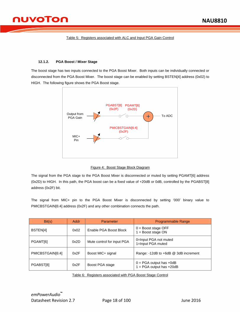
12.1.2. PGA Boost / Mixer Stage
The boost stage has two inputs connected to the PGA Boost Mixer. Both inputs can be individually connected or
disconnected from the PGA Boost Mixer. The boost stage can be enabled by setting BSTEN[4] address (0x02) to
HIGH. The following figure shows the PGA Boost stage.
PMICBSTGAIN[6:4]
(0x2F)
PGAMT[6]
(0x2D)
PGABST[8]
(0x2F)
Output from
PGA Gain
MIC+
Pin
To ADC
Figure 4: Boost Stage Block Diagram The signal from the PGA stage to the PGA Boost Mixer is disconnected or muted by setting PGAMT[6] address
(0x2D) to HIGH. In this path, the PGA boost can be a fixed value of +20dB or 0dB, controlled by the PGABST[8]
address (0x2F) bit.
The signal from MIC+ pin to the PGA Boost Mixer is disconnected by setting ‘000’ binary value to
PMICBSTGAIN[6:4] address (0x2F) and any other combination connects the path.
Bit(s) Addr Parameter Programmable Range
BSTEN[4] 0x02 Enable PGA Boost Block 0 = Boost stage OFF 1 = Boost stage ON
PGAMT[6] 0x2D Mute control for input PGA 0=Input PGA not muted 1=Input PGA muted
PMICBSTGAIN[6:4] 0x2F Boost MIC+ signal Range: -12dB to +6dB @ 3dB increment
PGABST[8] 0x2F Boost PGA stage 0 = PGA output has +0dB 1 = PGA output has +20dB
Table 6: Registers associated with PGA Boost Stage Control

NAU8810
emPowerAudio™ Datasheet Revision 2.7 Page 19 of 100 June 2016
12.2. MICROPHONE BIASING
Figure 5: Microphone Bias Schematic The MICBIAS pin is a low-noise microphone bias source for an external microphone, and it can provide a
maximum of 3mA of bias current. This DC bias voltage is suitable for powering either traditional ECM (electret)
type microphones, or for MEMS types microphones with an independent power supply pin. Seven different bias
voltages are available for optimum system performance, depending on the specific application. The microphone
bias pin normally requires an external filtering capacitor as shown on the schematic in the Application section.
The output bias can be enabled by setting MICBIASEN[4] address (0x01) to HIGH. It has various voltage values
selected by a combination of bits MICBIASM[4] address (0x3A) and MICBIASV[8:7] address (0x2C).
The low-noise feature results in greatly reduced noise in the external MICBIAS voltage by placing an internal
resistor of approximately 200-ohms in series with the output pin. This creates a low pass filter in conjunction with
the external microphone-bias filter capacitor, but without any other additional external components.
Bit(s) Addr Parameter Programmable Range
MICBIASEN[4] 0x01 Microphone bias enable 0 = Disable 1 = Enable
MICBIASM[4] (0x3A) Microphone bias mode selection
MICBIASV[8:7] (0x2C) Microphone bias voltage selection 0 = Disable 1 = Enable
Table 7: Register associated with Microphone Bias Below are the unloaded values when MICBIASM[4] is set to 1 and 0. When loaded, the series resistor will cause
the voltage to drop, depending on the load current.
R
VREF
R
MICBIAS
MICBIASM[0]
(0x28)
MICBIASV[1:0]
(0x2C)

NAU8810
emPowerAudio™ Datasheet Revision 2.7 Page 20 of 100 June 2016
Microphone Bias Voltage Control
MICBIASV[8:7] MICBIASM[4] = 0 MICBIASM[4]= 1
0 0 0.9* VDDA 0.85* VDDA
0 1 0.65* VDDA 0.60* VDDA
1 0 0.75* VDDA 0.70* VDDA
1 1 0.50* VDDA 0.50* VDDA
Table 8: Microphone Bias Voltage Control
12.3. ADC DIGITAL FILTER BLOCK
Figure 6: ADC Digital Filter Path Block Diagram The ADC digital filter block performs a 24-bit signal processing. The block consists of an oversampled analog
sigma-delta modulator, digital decimator, digital filter, 5-band graphic equalizer, high pass filter, and a notch filter.
For digital decimator and 5-band graphic equalizer details, refer to “Output Signal Path”. The oversampled analog
sigma-delta modulator provides a bit stream to the decimation stages and filter. The ADC coding scheme is in
twos-complement format, and the full-scale input level is proportional to VDDA. With a 3.3V supply voltage, the
full-scale level is 1.0VRMS and any voltage greater than full scale may overload the ADC and cause distortion.
The ADC is enabled by setting ADCEN[0] address (0x02) bit. Polarity and oversampling rate of the ADC output
signal can be changed by ADCPL[0] address (0x0E) and ADCOS[3] address (0x0E) respectively.
ADC Digital Filters
ADCDigital
Decimator/
Digital
FilterGain
5-Band
Equalizer
High
Pass
Filter
Notch
Filter
Digital
Audio
Interface

NAU8810
emPowerAudio™ Datasheet Revision 2.7 Page 21 of 100 June 2016
Bit(s) Addr Parameter Programmable Range
ADCPL[0] 0x0E ADC Polarity 0 = Normal 1 = Inverted
ADCOS[3] 0x0E ADC Over Sample
Rate
0=64x (Lowest power) 1=128x (best SNR at typical condition)
HPFEN[8] 0x0E High Pass Filter
Enable
0 = Disable 1 = Enable
HPFAM[7] 0x0E Audio or Application Mode 0 = Audio (1
st order, fc ~ 3.7 kHz)
1 = Application (2nd
order, fc =HPF)
HPF[6:4] 0x0E High Pass Filter frequencies 82 Hz to 612 Hz depending on the sample rate
ADCEN[0] 0x02 Enable ADC 0 = Disable 1 = Enable
SMPLR[3:1] 0x07 Sample rate 8k Hz to 48 kHz
Table 9: Register associated with ADC
12.3.1. Programmable High Pass Filter (HPF)
The high pass filter (HPF) has two different operational modes set by bit HPFAM[7] at address (0x0E). In Audio
Mode (HPFAM=0), the filter is first order, with a cut-off frequency of 3.7Hz. In Application mode (HPFAM=1), the
filter is second order, with a cut-off frequency selectable via the HPF[2:0] register bits. Cut-off frequency of the
HPF depends on sample frequency selected by SMPLR[3:1] address (0x07). The HPF is enabled by setting
HPFEN[8] address (0x0E) to HIGH. Table below shows the cut-off frequencies with different sampling rates.
HPF[2:0]
fs (kHz)
SMPLR=101/100 SMPLR=011/010 SMPLR=001/000
8 11.025 12 16 22.05 24 32 44.1 48
000 82 113 122 82 113 122 82 113 122
001 102 141 153 102 141 153 102 141 153
010 131 180 156 131 180 156 131 180 156
011 163 225 245 163 225 245 163 225 245
100 204 281 306 204 281 306 204 281 306
101 261 360 392 261 360 392 261 360 392
110 327 450 490 327 450 490 327 450 490
111 408 563 612 408 563 612 408 563 612
Table 10: High Pass Filter Cut-off Frequencies (HPFAM=1)

NAU8810
emPowerAudio™ Datasheet Revision 2.7 Page 22 of 100 June 2016
12.3.2. Programmable Notch Filter (NF)
The NAU88U10 has a programmable notch filter which passes all frequencies except those in a stop band
centered on a given center frequency. The filter gives lower distortion and flattens response. The notch filter is
enabled by setting NFCEN[7] address (0x1B) to HIGH. The variable center frequency is programmed by setting
two’s complement values to NFCA0[6:0] address (0x1C), NFCA0[13:7] address (0x1B) and NFCA1[6:0] address
(0x1E), NFCA1[13:7] address (0x1D) registers. The coefficients are updated in the circuit when the NFCU[8] bit
is set HIGH in a write to any of the registers NF1-NF4 address (0x1B, 0x1C, 0x1D, 0x1E).
Addr Bit 8 Bit 7 Bit 6 Bit5 Bit 4 Bit 3 Bit 2 Bit 1 Bit 0 Default
0x1B NFCU NFCEN NFCA0[13:7] 0x000
0x1C NFCU 0 NFCA0[6:0] 0x000
0x1D NFCU 0 NFCA1[13:7] 0x000
0x1E NFCU 0 NFCA1[6:0] 0x000
Table 11: Registers associated with Notch Filter Function
A0 A1 Notation Register Value (DEC)
Coefficient
s
b
s
b
f
f
f
f
2
21
2
21
tan
tan
s
c
f
fxA
21 0 cos
fc = center frequency (Hz) fb = -3dB bandwidth (Hz) fs = sample frequency (Hz)
NFCA0 = -A0 x 213
NFCA1 = -A1 x 2
12
(then convert to 2’s complement)
Table 12: Equations to Calculate Notch Filter Coefficients
12.3.3. Digital ADC Gain Control
The digital ADC can be muted by setting “0000 0000” to ADCGAIN[7:0] address (0x0F). Any other combination
digitally attenuates the ADC output signal in the range -127dB to 0dB in 0.5dB increments].
Addr Name Bit 8 Bit 7 Bit 6 Bit5 Bit 4 Bit 3 Bit 2 Bit 1 Bit 0 Default
0x0F ADCG 0 ADCGAIN 0x0FF
Table 13: Register associated with ADC Gain

NAU8810
emPowerAudio™ Datasheet Revision 2.7 Page 23 of 100 June 2016
12.4. PROGRAMMABLE GAIN AMPLIFIER (PGA)
NAU88U10 has a programmable gain amplifier (PGA) which controls the gain under program control, or
automatically supporting either of these two features:
Automatic level control (ALC) or
Input peak limiter
The Automatic Level Control (ALC) seeks to control the PGA gain in response to the amplitude of the input signal
such that the PGA output maintains a relatively constant level. The peak limiter simply prevents the output signal
from exceeding a specified level.
12.4.1. Automatic level control (ALC)
The ALC seeks to control the PGA gain such that the PGA output maintains a constant envelope. This helps to
prevent clipping at the input of the sigma delta ADC while maximizing the full dynamic range of the ADC. The
ALC monitors the output of the ADC, and adjusts the PGA gain as required. The ADC output is fed into a peak
detector, which updates the measured peak value whenever the absolute value of the input signal is higher than
the current measured peak. The measured peak gradually decays to zero unless a new peak is detected,
allowing for an accurate measurement of the signal envelope. Based on a comparison between the measured
peak value and the target value, the ALC block adjusts the gain control, which is fed back to the PGA.
Figure 7: ALC Block Diagram The ALC is enabled by setting ALCEN[8] address (0x20) bit to HIGH. The ALC has two functional modes, which
is set by ALCM[8] address (0x22).
Normal mode (ALCM = LOW)
Peak Limiter mode (ALCM = HIGH)
PGA ADC Sinc
Filter
Digital
Decimator
ALC
Rate Convert/ Decimator
Input
Pin
Digital
Filter

NAU8810
emPowerAudio™ Datasheet Revision 2.7 Page 24 of 100 June 2016
When the ALC is disabled, the input PGA remains at the last controlled value of the ALC. An input gain update
must be made by writing to the PGAGAIN[5:0] address (0x2D). A digital peak detector monitors the input signal
amplitude and compares it to a register defined threshold level ALCSL[3:0] address (0x21).
Blue Original Input signal (linear line from zero to maximum) Green PGA gain value over time (inverse to signal in target range)
Red Output signal (held to a constant value in target range)
Figure 8: ALC Response Graph The registers listed in the following section allow configuration of ALC operation with respect to:
ALC target level
Gain increment and decrement rates
Minimum and maximum PGA gain values for ALC operating range
Hold time before gain increments in response to input signal
Inhibition of gain increment during noise inputs
Limiter mode operation
ALC operation range
Target ALCSL -6dB
Gain (Attenuation) Clipped
at ALCMNGAIN -12dB
Ou
tpu
t L
eve
l
-39dB
-39dB -6dB +6dB
-12 dB
0 dB
+33 dB
Input Level
Input < noise
gate threshold
ALCNEN = 1
ALCNTH = -39dB
MIC Boost Gain = 0dB
ALCSL = -6dB
ALCMNGAIN = -12dB
ALCMXGAIN = +35.25dB
PGA Gain

NAU8810
emPowerAudio™ Datasheet Revision 2.7 Page 25 of 100 June 2016
Bit(s) Addr Parameter Programmable Range
ALCMNGAIN[2:0]
0x20
Minimum Gain of PGA Range: -12dB to +30dB @ 6dB increment
ALCMXGAIN[2:0] Maximum Gain of PGA Range: -6.75dB to +35.25dB @ 6dB increment
ALCEN[8] Enable ALC function 0 = Disable 1 = Enable
ALCSL[3:0]
0x21
ALC Target Range: -28.5dB to -6dB @ 1.5dB increment
ALCHT[3:0] ALC Hold Time Range: 0ms to 1s, time doubles with every step)
ALCZC[8] ALC Zero Crossing 0 = Disable 1 = Enable
ALCATK[3:0]
0x22
ALC Attack time ALCM=0 - Range: 125us to 128ms ALCM=1 - Range: 31us to 32ms (time doubles with every step)
ALCDCY[3:0] ALC Decay time ALCM=0 - Range: 500us to 512ms ALCM=1 - Range: 125us to 128ms (Both ALC time doubles with every step)
ALCM[8] ALC Select 0 = ALC mode 1 = Limiter mode
Table 14: Registers associated with ALC Control The operating range of the ALC is set by ALCMXGAIN[5:3] address (0x20) and ALCMNGAIN[2:0] address (0x20)
bits such that the PGA gain generated by the ALC is between the programmed minimum and maximum levels.
When the ALC is enabled, the PGA gain is disabled.
In Normal mode, the ALCMXGAIN bits set the maximum level for the PGA in the ALC mode but in the Limiter
mode ALCMXGAIN has no effect because the maximum level is set by the initial PGA gain setting upon enabling
of the ALC.
ALCMAXGAIN Maximum Gain (dB)
ALCMINGAIN Minimum Gain (dB)
111 35.25 000 -12
110 29.25 001 -6
ALC Max Gain Range 35.25dB to -6dB @ 6dB increments
ALC Min Gain Range -12dB to 30dB @
6dB increments
001 -0.75 110 24
000 -6.75 111 30
Table 15: ALC Maximum and Minimum Gain Values

NAU8810
emPowerAudio™ Datasheet Revision 2.7 Page 26 of 100 June 2016
12.4.1.1. Normal Mode
Normal mode is selected when ALCM[8] address (0x22) is set LOW and the ALC is enabled by setting ALCEN[8]
address (0x20) HIGH. This block adjusts the PGA gain setting up and down in response to the input level. A
peak detector circuit measures the envelope of the input signal and compares it to the target level set by
ALCSL[3:0] address (0x21). The ALC increases the gain when the measured envelope is greater than the target
and decreases the gain when the measured envelope is less than - 1.5dB. The following waveform illustrates the
behavior of the ALC.
Figure 9: ALC Normal Mode Operation
12.4.1.2. ALC Hold Time (Normal mode Only)
The hold parameter ALCHT[3:0] configures the time between detection of the input signal envelope being outside
of the target range and the actual gain increase.
Input signals with different characteristics (e.g., voice vs. music) may require different settings for this parameter
for optimal performance. Increasing the ALC hold time prevents the ALC from reacting too quickly to brief periods
of silence such as those that may appear in music recordings; having a shorter hold time, on the other hand, may
be useful in voice applications where a faster reaction time helps to adjust the volume setting for speakers with
different volumes. The waveform below shows the operation of the ALCHT parameter.
PGA Input
PGA Output
PGA Gain

NAU8810
emPowerAudio™ Datasheet Revision 2.7 Page 27 of 100 June 2016
Figure 10: ALC Hold Time
12.4.2. Peak Limiter Mode
Peak Limiter mode is selected when ALCM[8] address (0x22) is set to HIGH and the ALC is enabled by setting
ALCEN[8] address (0x20). In limiter mode, the PGA gain is constrained to be less than or equal to the gain
setting at the time the limiter mode is enabled. In addition, attack and decay times are faster in limiter mode than
in normal mode as indicated by the different lookup tables for these parameters for limiter mode. The following
waveform illustrates the behavior of the ALC in Limiter mode in response to changes in various ALC parameters.
Figure 11: ALC Limiter Mode Operations
When the input signal exceeds 87.5% of full scale, the ALC block ramps down the PGA gain at the maximum
attack rate (ALCATK=0000), regardless of the mode and attack rate settings until the ADC output level has been
reduced below this threshold. This minimizes ADC clipping, if there is a sudden increase in the input signal level.
Limiter
Enabled
PGA Gain
PGA Input
PGA
Output
Hold Delay
Change
PGA Gain
PGA Input
PGA Output

NAU8810
emPowerAudio™ Datasheet Revision 2.7 Page 28 of 100 June 2016
12.4.3. Attack Time
When the absolute value of the ADC output exceeds the level set by the ALC threshold, ALCSL[3:0] address
(0x21), attack mode is initiated at a rate controlled by the attack rate register ALCATK[3:0] address (0x22). The
peak detector in the ALC block loads the ADC output value when the absolute value of the ADC output exceeds
the current measured peak; otherwise, the peak decays towards zero, until a new peak has been identified. This
sequence is continuously running. If the peak is ever below the target threshold, then there is no gain decrease
at the next attack timer time; if it is ever above the target-1.5dB, then there is no gain increase at the next decay
timer time.
12.4.4. Decay Times
The decay time ALCDCY[6:4] address (0x22) is the time constant used when the gain is increasing. In limiter
mode, the time constants are faster than in ALC mode.
12.4.5. Noise gate (normal mode only)
A noise gate may be used to limit the ALC gain when there is no input signal, or a signal less than the noise gate
threshold. This noise from excess input gain, when there is no useful signal to amplify. The noise gate is enabled
by setting ALCNEN[3] address (0x23) to HIGH. It does not remove noise from the signal. The noise gate
threshold ALCNTH[2:0] address (0x23) is set to a desired level so when there is no signal or a very quiet signal
(pause), which is composed mostly of noise, the ALC holds the gain constant instead of amplifying the signal
towards the target threshold. The noise gate only operates in conjunction with the ALC and ONLY in Normal
mode. The noise gate flag is asserted when
(Signal at ADC – PGA gain – MIC Boost gain) < ALCNTH (ALC Noise Gate Threshold) (dB)
Levels at the extremes of the range may cause inappropriate operation, so care should be taken when setting up
the function.
Figure 12: ALC Operation with Noise Gate disabled
PGA Input
PGA Output
PGA Gain

NAU8810
emPowerAudio™ Datasheet Revision 2.7 Page 29 of 100 June 2016
Figure 13: ALC Operation with Noise Gate Enabled
12.4.6. Zero Crossing
The PGA gain comes from either the ALC block when the ALC is enabled, or directly from the PGA gain register
setting when the ALC is disabled. Zero crossing detection may be enabled to force PGA gain changes to occur
only at an input zero crossing event. Enabling zero crossing detection limits clicks and pops that will occur if the
gain changes while the input signal is at a voltage that is significantly higher or lower than zero.
There are two zero crossing detection enables:
Register ALCZC[8] address (0x21) – is only relevant when the ALC is enabled.
Register PGAZC[7] address (0x2D) – is only relevant when the ALC is disabled.
If the zero crossing function is enabled (using either register) and SCLKEN[0] address (0x07) is asserted, the zero
cross timeout function may take effect. If the zero crossing flag does not change polarity within 0.25 seconds of a
PGA gain update (either via ALC update or PGA gain register update), then the gain will update automatically.
This backup system prevents the gain from locking up if the input signal has a small swing and/or a DC offset that
prevents the zero crossing flag from triggering.
PGA Input
PGA Output
PGA Gain
Noise Gate Threshold

NAU8810
emPowerAudio™ Datasheet Revision 2.7 Page 30 of 100 June 2016
12.5. DAC DIGITAL FILTER BLOCK
Figure 14: DAC Digital Filter Path The DAC digital block uses 24-bit signal processing to generate analog audio using data from the audio data bus
or from the ADC output. This block consists of a sigma-delta modulator, 5-band graphic equalizer, high pass filter,
digital gain/filters, de-emphasis, and analog mixers. The DAC coding scheme is in twos complement format and
the full-scale output level is proportional to VDDA. With a 3.3V supply voltage, the full-scale output level is
1.0VRMS. The DAC is enabled by setting DACEN[0] address (0x03) bit HIGH.
Bit(s) Addr Parameter Programmable Range
DACEN[0] 0x03 DAC enable 0 = Disable
1 = Enable
ADDAP[0] 0x05 Pass-through of ADC output data into DAC input
0 = Disable
1 = Enable
DACPL[0]
0x0A
DAC Polarity 0 = No Inversion
1 = DAC Output Inverted
AUTOMT[2] Auto Mute 0 = Disable
1 = Enable
DEEMP[5:4] Sample Rate 32 kHz, 44.1 kHz, and 48 kHz
DACMT[6] Soft Mute 0 = Disable
1 = Enable
DACGAIN[7:0] 0x0B DAC Volume Control Range: -127dB to 0dB @ 0.5dB increment, 00 hex is Muted
DACLIMATK[3:0]
0x18
DAC Limiter Attack Range: 68us to 139ms
DACLIMDCY[7:4] DAC Limiter Decay Range: 544us to 1.1s
DACLIMEN[8] DAC Limiter Enable 0 = Disable
1 = Enable
DACLIMBST[3:0] 0x19
DAC Limiter Volume Boost Range: 0dB to +12dB @ 1dB increment
DACLIMTHL[6:4] DAC Limiter Threshold Range: -6dB to -1bB @ 1dB increment
Table 16: Registers associated with DAC Gain Control
Digital
Gain
Digital
Peak
Limiter
Digital
Filters
Interpo-
lation
Sigma
Delta
Modulator
DAC Digital Filters
Digital
Audio
Interface
5-Band
EqualizerDAC
NAU8810
emPowerAudio™ Datasheet Revision 2.7 Page 31 of 100 June 2016
12.5.1. DAC Soft Mute
The NAU88U10 also has a Soft Mute function, which smoothly attenuates the volume of the digital signal to zero.
When un-muted, the gain will ramp back up to the register determined digital gain setting. This feature provides a
tool that is useful to enable/disable DAC output without introducing pop and click sounds. To output any DAC
signal, Soft Mute must be disabled by setting the DACMT[6] address (0x0A) bit to LOW.
12.5.2. DAC Auto Mute
The output of the DAC can also be muted by the analog Auto Mute function. The Auto Mute function is enabled
by setting AUTOMT[2] address (0x0A) to HIGH and applied to the DAC output when there are 1024 or more
consecutive zeros at its input. If at any time there is a non-zero DAC input sample value, the DAC will be un-
muted, and the 1024 count will be reinitialized to zero.
12.5.3. DAC Sampling / Oversampling rate, Polarity, DAC Volume control and Digital Pass-through
The sampling rate of the DAC is determined entirely by the frequency of its input clock and the oversampling rate
setting. The oversampling rate of the DAC can be changed to 64x or 128x. In the 128x oversampling mode,
audio performance is improved at slightly higher power consumption. Because the additional supply current is
only 1mA, in most applications, the 128x oversampling is preferred for maximum audio performance.
The polarity of the DAC output signal can be changed as a feature, and this can useful in management of the
audio phase. This feature can help minimize audio processing that may be otherwise required as the data are
passed to other stages in the system.
The effective output audio volume of the DAC can be changed using the digital volume control feature. This
processes the output of the DAC to scale the output by the amount indicated in the volume register setting.
Included is a “digital mute” value which will completely mute the signal output of the DAC. The digital volume
setting can range from 0dB through -127dB in 0.5dB steps.
Digital audio pass-through allows the output of the ADC to be directly sent to the DAC as the input signal to the
DAC for DAC output. In this mode of operation, the external digital audio signal for the DAC will be ignored. The
pass-through function is useful for many test and application purposes, and the DAC output may be utilized in any
way that is normally supported for the DAC analog output signals.

NAU8810
emPowerAudio™ Datasheet Revision 2.7 Page 32 of 100 June 2016
12.5.4. Hi-Fi DAC De-Emphasis and Gain Control
The NAU88U10 has Hi-Fi DAC gain control for signal conditioning. The level of attenuation for an eight-bit code
X is given by: 0.5 × (X-255) dB for 1 ≤ X ≤ 255; MUTE for X = 0
It includes on-chip digital de-emphasis and is available for sample rates of 32 kHz, 44.1 kHz, and 48 kHz. The
digital de-emphasis can be enabled by setting DEEMP[5:4] address (0x0A) bits depending on the input sample
rate. The de-emphasis feature is included to accommodate audio recordings that utilize 50/15 s pre-emphasis
equalization as a means of noise reduction.
12.5.5. Digital DAC Output Peak Limiter
Output Peak-Limiters optimize the dynamic range by ensuring the signal will not exceed a certain threshold, while
maximizing the RMS of the resulted audio signal, and minimizing audible distortions. NAU88U10 has a digital
output limiter function. The operation of this is shown in figure below. In this diagram, the upper graph shows the
envelope of the input/output signals and the lower graph shows the gain characteristic. The limiter has a
programmable threshold, DACLIMTHL[6:4] address (0x19), which ranges from -1dB to -6dB in 1dB increments.
The digital peak limiter seeks to keep the envelope of the output signal within the target threshold +/- 0.5dB. The
attack and decay rates programmed in registers DACLIMATK[3:0] address (0x18) and DACLIMDCY[7:4] address
(0x18) specify how fast the digital peak limiter decrease and increase the gain, respectively, in response to the
envelope of the output signal falling outside of this range. In normal operation LIMBST=000 signals below this
threshold are unaffected by the limiter.
Figure 15: DAC Digital Limiter Control
12.5.6. Volume Boost
DAC Input
Data
DAC Output
Signal
Digital Gain0dB
-1dB
-0.5dB
Threshold
-1dB

NAU8810
emPowerAudio™ Datasheet Revision 2.7 Page 33 of 100 June 2016
The limiter has programmable upper gain, which boosts signals below the threshold to compress the dynamic
range of the signal and increase its perceived loudness. This operates as an ALC function with limited boost
capability. The volume boost is from 0dB to +12dB in 1dB steps, controlled by the DACLIMBST[3:0] register bits.
The output limiter volume boost can also be used as a stand-alone digital gain boost when the limiter is disabled.
12.5.7. 5-Band Equalizer
NAU88U10 features 5-band graphic equalizer with low distortion, low noise, and wide dynamic range, and is an
ideal choice for Hi-Fi applications. All five bands are fully parametric with independently adjustable bandwidth
that displays exceptional tonal qualities. Each of the five bands offers +/- 12dB of boost and cut with 1dB
resolution. The five bands are divided in to three sections Low, Mid and High bands. The High and the Low
bands are shelving filters and the mid three are peak filters. The equalizer can be applied to the ADC or DAC
path under control of the EQM[8] address (0x12) register bit.
Bit(s) Address Parameter Programmable Range
EQM[8]
0x12
Equalizer Enable
EQ1CF[6:5] Band 1 Cut-off Frequency Range: 80 Hz to 175 Hz
EQ1GC[4:0] Band 1 Gain Control Range: -12 dB to +12 dB @ 1.0dB increment
EQ2BW[8]
0x13
Band 2 Equalizer Bandwidth Narrow or Wide
EQ2CF[6:5] Band 2 Centre Frequency Range: 230 Hz to 500 Hz
EQ2GC[4:0] Band 2 Gain Control Range: -12 dB to +12 dB @ 1.0dB increment
EQ2BW[8]
0x14
Band 3 Equalizer Bandwidth Narrow or Wide
EQ3CF[6:5] Band 3 Centre Frequency Range: 650 Hz to 1.4 kHz
EQ3GC[4:0] Band 3 Gain Control Range: -12 dB to +12 dB @ 1.0dB increment
EQ4BW[8]
0x15
Band 4 Equalizer Bandwidth Narrow or Wide
EQ4CF[6:5] Band 4 Centre Frequency Range: 1.8 kHz to 4.1 kHz
EQ4GC[4:0] Band 4 Gain Control Range: -12 dB to +12 dB @ 1.0dB increment
EQ5CF[6:5]
0x16
Band 5 Cut-off Frequency Range: 5.3 kHz to 11.7 kHz
EQ5GC[4:0] Band 5 Gain Control Range: -12 dB to +12 dB @ 1.0dB increment
Table 17: Registers associated with Equalizer Control

NAU8810
emPowerAudio™ Datasheet Revision 2.7 Page 34 of 100 June 2016
12.6. ANALOG OUTPUTS
The NAU88U10 features two different types of outputs, a single-ended or differential Mono output (MOUT) and a
differential speaker outputs (SPKOUT+ and SPKOUT-). The speaker amplifiers designed to drive a load
differentially; a configuration referred to as Bridge-Tied Load (BTL).
Figure 16: Speaker and MONO Analogue Outputs [To Update ? output from Auxilliary Amplifier]
Important: For analog outputs depopping purpose, when powering up speakers, headphone, AUXOUTs, certain delays are generated after enabling sequence. However, the delays are created by MCLK and sample rate register. For correct operation, sending I2S signal no earlier than 250ms after speaker or headphone enabled and MCLK appearing
12.6.1. Speaker Mixer Outputs
The speaker amplifiers are designed to drive a load differentially; a configuration referred to as Bridge-Tied Load
(BTL). The differential speaker outputs can drive a single 8Ω speaker or two headphone loads of 16Ω or higher,
including differential line output applications. Driving the load differentially doubles the output voltage. The output
of the speaker can be manipulated by changing attenuation and the volume (loudness of the output signal).
The output stage is powered by the speaker supply, VDDSPK, which are capable of driving up to 1.5VRMS signals
(equivalent to 3VRMS into a BTL speaker). The speaker outputs can be controlled and can be muted individually.
The output pins are at reference DC level when the output is muted.
-10dB or +0dB
-10dB or 0dB
DAC Output
SIDETONE
Output from PGA Boost
MONO
MIXER
SPEAKER
MIXER
SPKOUT+
MOUT
VSSSPK
-1
VDDSPK
SPKBST[2]
(0x31)
SPKOUT-
Zero Cross
Detection
Output from
Auxiliary Amplifier
VSSSPK
VDDSPK
SPKBST
0
1
GAIN
1.0x
1.5x
MOUTBST
0
1
GAIN
1.0x
1.5x
DC output
1.0 x VREF
1.5 x VREF
SPKVOL[5:0]
(0x36)
MOUTBST[3]
(0x31)
SPKMXEN[2]
(0x03)
DACOUT[0]
(0x38)
Zero Cross
Detection
Buffer
DC output
1.0 x VREF
1.5 x VREF
MOUTMXEN[3]
(0x03)

NAU8810
emPowerAudio™ Datasheet Revision 2.7 Page 35 of 100 June 2016
Bit(s) Addr Parameter Programmable Range
SPKMXEN[2] 0x03 Speaker Mixer enable 0 – Disabled 1 – Enabled
PSPKEN[5] 0x03 Speaker positive terminal enable
0 – Disabled 1 – Enabled
NSPKEN[6] 0x03 Speaker negative terminal enable
0 – Disabled 1 – Enabled
SPKATT[1] 0x28 Speaker output attenuation 0 - 0dB 1 - -10dB
SPKBST[2] 0x31 Speaker output Boost 0 – (1.0x VREF) Boost 1- (1.5 x VREF) Boost
SPKGAIN[5:0] 0x36 Speaker output Volume Range: -57dB to +6dB @ 6dB increment
SPKMT[6] 0x36 Speaker output Mute 0 – Speaker Enabled 1 – Speaker Muted
Table 18: Speaker Output Controls
12.6.2. Mono Mixer Output
The single ended output can drive headphone loads of 16Ω or 32Ω or a line output. The MOUT can be
manipulated by changing attenuation and the volume (loudness of the output signal).
The output stage is powered by the speaker supply, VDDSPK, which are capable of driving up to 1.5VRMS signals.
The Mono output can be enabled for signal output or muted. The output pins are at reference DC level when the
output is muted.
Bit(s) Addr Parameter Programmable Range
MOUTMXEN[3] 0x03 MONO mixer enable 0 – Disabled 1 – Enabled
MOUTEN[7] 0x03 MONO output enable 0 – Disabled 1 – Enabled
MOUTATT[2] 0x28 MONO output attenuation 0 - 0dB 1 - -10dB
MOUTBST[3] 0x31 MONO output boost 0 – (1.0x VREF) Boost 1 - (1.5 x VREF) Boost
MOUTMXMT[6] 0x38 MONO Output Mixer Mute 0 – MONO Mixer Normal Mode 1 – MONO Mixer Muted
MOUTMT[4] 0x45 MONO Output Mute 0 – MONO Output Normal Mode 1 – MONO Output Muted
Table 19: MONO Output Controls

NAU8810
emPowerAudio™ Datasheet Revision 2.7 Page 36 of 100 June 2016
12.6.3. Differential Output Configuration
The NAU88U10 features two different types of outputs, a single-ended or differential Mono output (MOUT) and a
differential speaker output (SPKOUT+ and SPKOUT-). The speaker amplifiers are designed to drive a load
differentially as Bridge-Tied Load (BTL).
Three differential output options can be configured from the three output pins: MOUT, SPKOUT+ and SPKOUT-
. To enable differential outputs, three registers need to be configured accordingly: SPK2MOUT=1 (0x45[5]),
AOUTMP=1 (0x31[0]) and 0x4F=0x100.
- Option 1: Two differential outputs by using pair of MOUT and SPKOUT-, SPKOUT+ and SPKOUT- for driving
both headphone/earpiece and Speaker. Register setting: MOUTEN=1, NSPKEN=1, and PSPKEN =1
- Option 2: One differential output by using MOUT and SPKOUT- for driving headphone/earpiece. Register
setting: MOUTEN=1, NSPKEN=1, and PSPKEN =0
- Option 3: One differential output by using SPKOUT+ and SPKOUT- for driving speaker. Register setting:
MOUTEN=0, NSPKEN=1 and PSPKEN =1
12.6.4. Unused Analog I/O
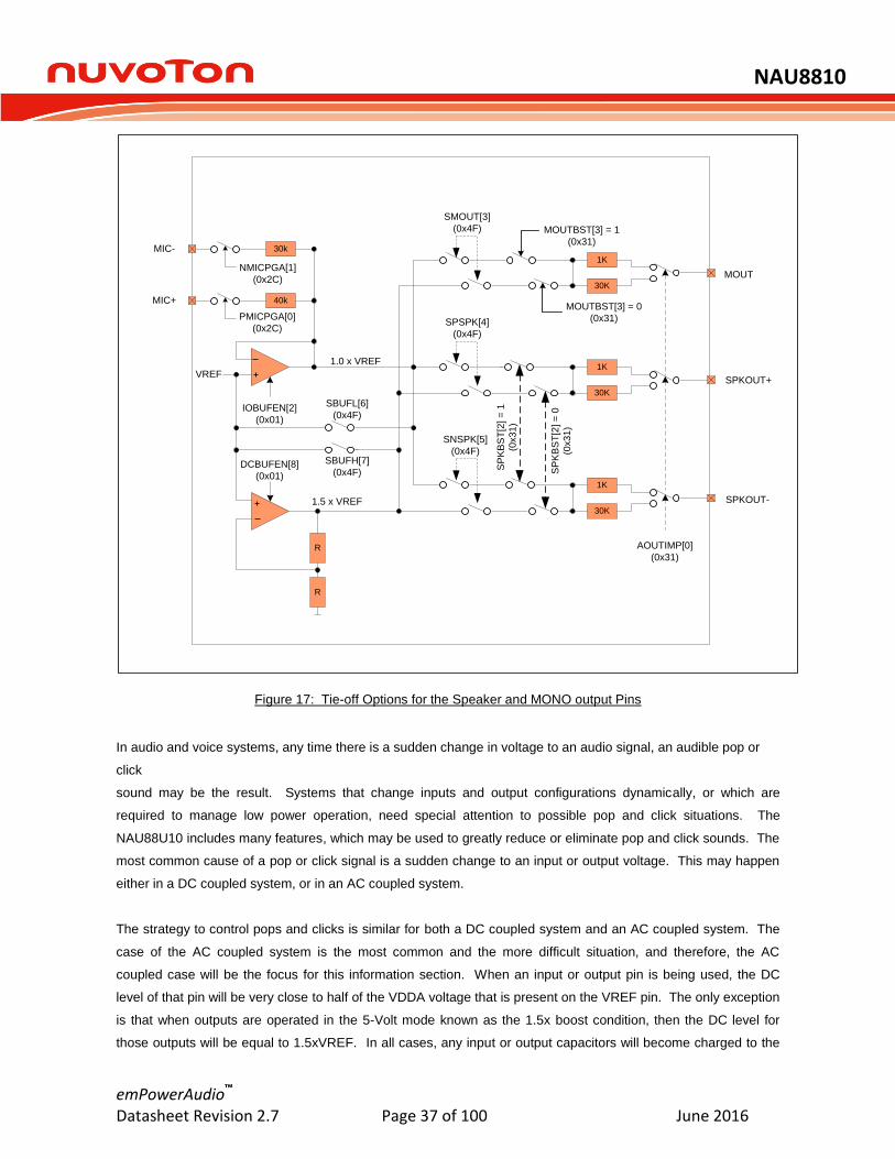
NAU8810
emPowerAudio™ Datasheet Revision 2.7 Page 37 of 100 June 2016
1K
30K
1K
30K
1K
30K
30k
40k
VREF
MIC-
MIC+
MOUT
SPKOUT+
SPKOUT-
R
R
IOBUFEN[2]
(0x01)
DCBUFEN[8]
(0x01)
AOUTIMP[0]
(0x31)
1.5 x VREF
1.0 x VREF
PMICPGA[0]
(0x2C)
NMICPGA[1]
(0x2C)
MOUTBST[3] = 1
(0x31)
MOUTBST[3] = 0
(0x31)
SP
KB
ST
[2] =
0
(0x3
1)
SP
KB
ST
[2] =
1
(0x3
1)
SMOUT[3]
(0x4F)
SPSPK[4]
(0x4F)
SNSPK[5]
(0x4F)SBUFH[7]
(0x4F)
SBUFL[6]
(0x4F)
Figure 17: Tie-off Options for the Speaker and MONO output Pins
In audio and voice systems, any time there is a sudden change in voltage to an audio signal, an audible pop or
click
sound may be the result. Systems that change inputs and output configurations dynamically, or which are
required to manage low power operation, need special attention to possible pop and click situations. The
NAU88U10 includes many features, which may be used to greatly reduce or eliminate pop and click sounds. The
most common cause of a pop or click signal is a sudden change to an input or output voltage. This may happen
either in a DC coupled system, or in an AC coupled system.
The strategy to control pops and clicks is similar for both a DC coupled system and an AC coupled system. The
case of the AC coupled system is the most common and the more difficult situation, and therefore, the AC
coupled case will be the focus for this information section. When an input or output pin is being used, the DC
level of that pin will be very close to half of the VDDA voltage that is present on the VREF pin. The only exception
is that when outputs are operated in the 5-Volt mode known as the 1.5x boost condition, then the DC level for
those outputs will be equal to 1.5xVREF. In all cases, any input or output capacitors will become charged to the

NAU8810
emPowerAudio™ Datasheet Revision 2.7 Page 38 of 100 June 2016
operating voltage of the used input or output pin. The goal to reduce pops and clicks is to insure that the charge
voltage on these capacitors does not change suddenly at any time.
When an input or output is in a not-used operating condition, it is desirable to keep the DC voltage on that pin at
the same voltage level as the DC level of the used operating condition. This is accomplished using special
internal DC voltage sources that are at the required DC values. When an input or output is in the not-used
condition, it is connected to the correct internal DC voltage as not to have a pop or click. This type of connection
is known as a “tie-off” condition.
Two internal DC voltage sources are provided for making tie-off connections. One DC level is equal to the VREF
voltage value, and the other DC level is equal to 1.5x the VREF value. All inputs are always tied off to the VREF
voltage value. Outputs will automatically be tied to either the VREF voltage value or to the 1.5xVREF value,
depending on the value of the “boost” control bit for that output. That is to say, when an output is set to the 1.5x
gain condition, then that same output will automatically use the 1.5xVREF value for tie-off in the not-used
condition. The input pull-ups are connected to IOBUFEN[2] address (0x01) buffer with a voltage source (VREF).
The output pull-ups can be connected two different buffers depending on the voltage source. IOBUFEN[2]
address (0x01) buffer is enabled if the voltage source is (VREF) and DCBUFEN[8] address (0x01) buffer is
enabled if the voltage source is (1.5 x VREF). IOBUFEN[2] address (0x01) buffer is shared between input and
output pins.
To conserve power, these internal voltage buffers may be enabled/disabled using control register settings. To
better manage pops and clicks, there is a choice of impedance of the tie-off connection for unused outputs. The
nominal values for this choice are 1kΩ and 30kΩ. The low impedance value will better maintain the desired DC
level in the case when there is some leakage on the output capacitor or some DC resistance to ground at the
NAU88U10 output pin. A tradeoff in using the low-impedance value is primarily that output capacitors could
change more suddenly during power-on and power-off changes.
Automatic internal logic determines whether an input or output pin is in the used or un-used condition. This logic
function is always active. An output is determined to be in the un-used condition when it is in the disabled
unpowered condition, as determined by the power management registers. An input is determined to be in the un-
used condition when all internal switches connected to that input are in the “open” condition.
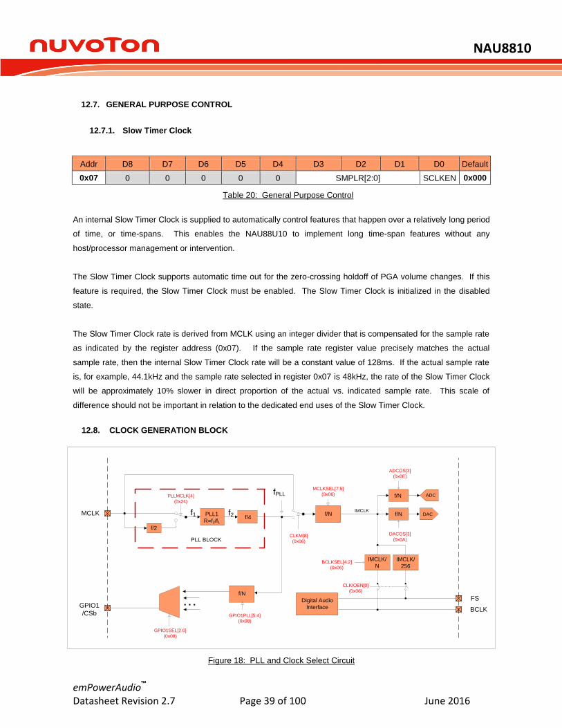
NAU8810
emPowerAudio™ Datasheet Revision 2.7 Page 39 of 100 June 2016
12.7. GENERAL PURPOSE CONTROL
12.7.1. Slow Timer Clock
Addr D8 D7 D6 D5 D4 D3 D2 D1 D0 Default
0x07 0 0 0 0 0 SMPLR[2:0] SCLKEN 0x000
Table 20: General Purpose Control
An internal Slow Timer Clock is supplied to automatically control features that happen over a relatively long period
of time, or time-spans. This enables the NAU88U10 to implement long time-span features without any
host/processor management or intervention.
The Slow Timer Clock supports automatic time out for the zero-crossing holdoff of PGA volume changes. If this
feature is required, the Slow Timer Clock must be enabled. The Slow Timer Clock is initialized in the disabled
state.
The Slow Timer Clock rate is derived from MCLK using an integer divider that is compensated for the sample rate
as indicated by the register address (0x07). If the sample rate register value precisely matches the actual
sample rate, then the internal Slow Timer Clock rate will be a constant value of 128ms. If the actual sample rate
is, for example, 44.1kHz and the sample rate selected in register 0x07 is 48kHz, the rate of the Slow Timer Clock
will be approximately 10% slower in direct proportion of the actual vs. indicated sample rate. This scale of
difference should not be important in relation to the dedicated end uses of the Slow Timer Clock.
12.8. CLOCK GENERATION BLOCK
Figure 18: PLL and Clock Select Circuit
MCLK
f/2
PLL1
R=f2/f1f/4
f1 f2
fPLL
f/N
…GPIO1
/CSb GPIO1PLL[5:4]
(0x08)
PLLMCLK[4]
(0x24)
f/N
MCLKSEL[7:5]
(0x06) f/N
GPIO1SEL[2:0]
(0x08)
CLKIOEN[0]
(0x06)
FS
BCLK
BCLKSEL[4:2]
(0x06)
DACOS[3]
(0x0A)
ADCOS[3]
(0x0E)
PLL BLOCKCLKM[8]
(0x06)
IMCLK/
256
IMCLK/
N
ADC
DACf/N
Digital Audio
Interface
IMCLK

NAU8810
emPowerAudio™ Datasheet Revision 2.7 Page 40 of 100 June 2016
The NAU88U10 has two basic clock modes that support the ADC and DAC data converters. It can accept
external clocks in the slave mode, or in the master mode, it can generate the required clocks from an external
reference frequency using an internal PLL (Phase Locked Loop). The internal PLL is a fractional type scaling PLL,
and therefore, a very wide range of external reference frequencies can be used to create accurate audio sample
rates.
Separate from this ADC and DAC clock subsystem, audio data are clocked to and from the NAU88U10 by means
of the control logic described in the Digital Audio Interfaces section. The Frame Sync (FS) and Bit Clock (BCLK)
pins in the Digital Audio Interface manage the audio bit rate and audio sample rate for this data flow.
It is important to understand that the Digital Audio Interface does not determine the sampling rate for the ADC and
DAC data converters, and instead, this rate is derived exclusively from the Internal Master Clock (IMCLK). It is
therefore a requirement that the Digital Audio Interface and data converters be operated synchronously, and that
the FS, BCLK, and IMCLK signals are all derived from a common reference frequency. If these three clocks
signals are not synchronous, audio quality will be reduced.
The IMCLK is always exactly 256 times the sampling rate of the data converters. IMCLK is output from the
Master Clock Prescaler. The prescaler reduces by an integer division factor the input frequency input clock. The
source of this input frequency clock is either the external MCLK pin, or the output from the internal PLL Block.
Addr D8 D7 D6 D5 D4 D3 D2 D1 D0 Default
0x01 DCBUFEN 0 PLLEN MICBIASEN ABIASEN IOBUFEN REFIMP
0x06 CLKM MCLKSEL[2:0] BCLKSEL[2:0] 0 CLKIOEN 0x140
0x07 0 0 0 0 0 SMPLR[2:0] SCLKEN 0x000
0x24 0 0 0 0 PLLMCLK PLLN[3:0] 0x008
0x25 0 0 0 PLLK[23:18] 0x00C
0x26 PLLK[17:9] 0x093
0x27 PLLK[8:0] 0x0E9
Table 21: Registers associated with PLL
In Master Mode, the IMCLK signal is used to generate FS and BCLK signals that are driven onto the FS and
BCLK pins and input to the Digital Audio Interface. FS is always IMCLK/256 and the duty cycle of FS is
automatically adjusted to be correct for the mode selected in the Digital Audio Interface. The frequency of BCLK
may optionally be divided to optimize the bit clock rate for the application scenario.
In Slave Mode, there is no connection between IMCLK and the FS and BCLK pins. In this mode, FS and BLCK
are strictly input pins, and it is the responsibility of the system designer to insure that FS, BCLK, and IMCLK are
synchronous and scaled appropriately for the application.

NAU8810
emPowerAudio™ Datasheet Revision 2.7 Page 41 of 100 June 2016
12.8.1. Phase Locked Loop (PLL) General description
The PLL may be optionally used to multiply an external input clock reference frequency by a high resolution
fractional number. To enable the use of the widest possible range of external reference clocks, the PLL block
includes an optional divide-by-two prescaler for the input clock, a fixed divide-by-four scaler on the PLL output,
and an additional programmable integer divider that is the Master Clock Prescaler.
The high resolution fraction for the PLL is the ratio of the desired PLL oscillator frequency (f2), and the reference
frequency at the PLL input (f1). This can be represented as R = f2/f1, with R in the form of a decimal number:
xy.abcdefgh. To program the NAU88U10, this value is separated into an integer portion (“xy”), and a fractional
portion, “abcdefgh”. The fractional portion of the multiplier is a value that when represented as a 24-bit binary
number (stored in three 9-bit registers on the NAU88U10), very closely matches the exact desired multiplier factor.
To keep the PLL within its optimal operating range, the integer portion of the decimal number (“xy”), must be any
of the following decimal values: 6, 7, 8, 9, 10, 11, or 12. The input and output dividers outside of the PLL are
often helpful to scale frequencies as needed to keep the “xy” value within the required range. Also, the optimum
PLL oscillator frequency is in the range between 90MHz and 100MHz, and thus, it is best to keep f2 within this
range.
In summary, for any given design, choose:
Equations Description Notes
IMCLK = (256) * (desired codec sample rate)
IMCLK = desired Master Clock
f2 = (4 * P * IMCLK) where P is the Master Clock divider integer value; optimal f2: 90MHz< f2 <100MHz
The integer values for D and P are chosen to keep the PLL in its optimal operating range. It may be best to assign initial values of 1 to both D and P, and then by inspection, determine if they should be a different value.
f1 = (MCLK / D)
where D is the PLL Prescale factor of 1, or 2, and MCLK is the frequency at the MCLK pin
R = f2 / f1 = xy.abcdefgh decimal value
which is the fractional frequency multiplication factor for the PLL
N = xy truncated integer portion of the R value and limited to decimal value 6, 7, 8, 9, 10, 11, or 12
K = (224
) * (0.abcdefgh) rounded to the nearest whole integer value then converted to a binary 24-bit value
Table 22: Registers associated with PLL

NAU8810
emPowerAudio™ Datasheet Revision 2.7 Page 42 of 100 June 2016
12.8.2. Phase Locked Loop (PLL) Design Example
In an example application, a desired sample rate for the DAC is known to be 48.000kHz. Therefore, it is also
known that the IMCLK rate will be 256fs, or 12.288MHz. Because there is a fixed divide-by-four scaler on the PLL
output, then the desired PLL oscillator output frequency will be 49.152MHz.
In this example system design, there is any an available 12.000MHz clock from the USB subystem. To reduce
system cost, this clock will also be used for audio. Therefore, to use the 12MHz clock for audio, the desired
fractional multiplier ratio would be R = 49.152/12.000 = 4.096. This value, however, does not meet the
requirement that the “xy” whole number portion of the multiplier be in the inclusive range between 6 and 12. To
meet the requirement, the Master Clock Prescaler can be set for an additional divide-by-two factor. This now
makes the PLL required oscillator frequency 98.304 MHz, and the improved multiplier value is now R =
98.304/12.000 = 8.192.
To complete this portion of the design example, the integer portion of the multiplier is truncated to the value, 8 and
the fractional portion is multiplied by 224
, as to create the needed 24-bit binary fractional value. The calculation for
this is: (224
)(0.192) = 3221225.472.
It is best to round this value to the nearest whole value of 3221225, or hexadecimal 0x3126E9.
Below are additional examples of results for this calculation applied to commonly available clock frequencies and
desired IMCLK 256fs sample rates.
MCLK (MHz)
Desired Output (MHz)
Input Frequency
(f1)
f2 (MHz)
MCLK Divider
bits R
N (Hex)
K (Hex) Actual Register Setting
PLLK[23:18] PLLK[17:9] PLLK[8:0]
12.0 11.28960 MCLK/1 90.3168 fPLL/2 7.526400 7 86C226 21 161 26
12.0 12.28800 MCLK/1 98.3040 fPLL/2 8.192000 8 3126E9 0C 93 E9
14.4 11.28960 MCLK/1 90.3168 fPLL/2 6.272000 6 45A1CA 11 D0 1CA
14.4 12.28800 MCLK/1 98.3040 fPLL/2 6.826667 6 D3A06D 34 1D0 6D
19.2 11.28960 MCLK/2 90.3168 fPLL/2 9.408000 9 6872B0 1A 39 B0
19.2 12.28800 MCLK/2 98.3040 fPLL/2 10.240000 10 3D70A3 0F B8 A3
19.8 11.28960 MCLK/2 90.3168 fPLL/2 9.122909 9 1F76F8 07 1BB F8
19.8 12.28800 MCLK/2 98.3040 fPLL/2 9.929697 9 EE009E 3B 100 9E
24.0 11.28960 MCLK/2 90.3168 fPLL/2 7.526400 7 86C226 21 161 26
24.0 12.28800 MCLK/2 98.3040 fPLL/2 8.192000 8 3126E9 0C 93 E9
26.0 11.28960 MCLK/2 90.3168 fPLL/2 6.947446 6 F28BD4 3C 145 1D4
26.0 12.28800 MCLK/2 98.3040 fPLL/2 7.561846 7 8FD526 23 1EA 126
Table 23: PLL Frequency Examples
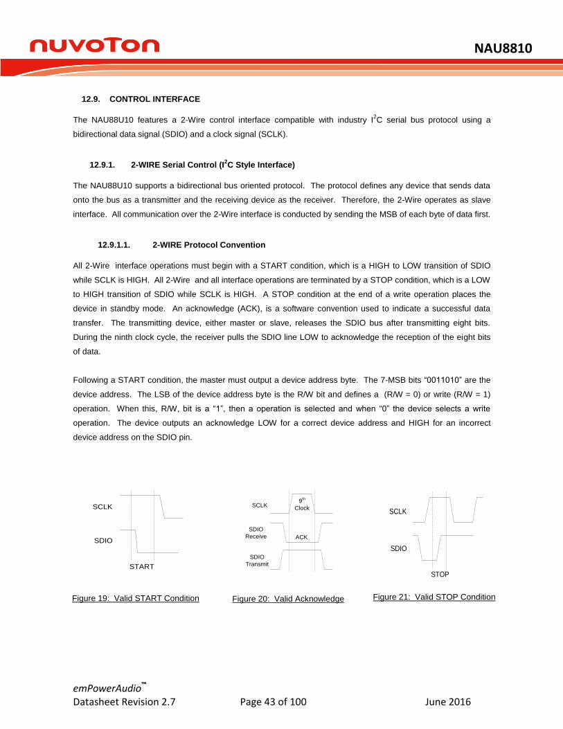
NAU8810
emPowerAudio™ Datasheet Revision 2.7 Page 43 of 100 June 2016
12.9. CONTROL INTERFACE
The NAU88U10 features a 2-Wire control interface compatible with industry I2C serial bus protocol using a
bidirectional data signal (SDIO) and a clock signal (SCLK).
12.9.1. 2-WIRE Serial Control (I2C Style Interface)
The NAU88U10 supports a bidirectional bus oriented protocol. The protocol defines any device that sends data
onto the bus as a transmitter and the receiving device as the receiver. Therefore, the 2-Wire operates as slave
interface. All communication over the 2-Wire interface is conducted by sending the MSB of each byte of data first.
12.9.1.1. 2-WIRE Protocol Convention
All 2-Wire interface operations must begin with a START condition, which is a HIGH to LOW transition of SDIO
while SCLK is HIGH. All 2-Wire and all interface operations are terminated by a STOP condition, which is a LOW
to HIGH transition of SDIO while SCLK is HIGH. A STOP condition at the end of a write operation places the
device in standby mode. An acknowledge (ACK), is a software convention used to indicate a successful data
transfer. The transmitting device, either master or slave, releases the SDIO bus after transmitting eight bits.
During the ninth clock cycle, the receiver pulls the SDIO line LOW to acknowledge the reception of the eight bits
of data.
Following a START condition, the master must output a device address byte. The 7-MSB bits “0011010” are the
device address. The LSB of the device address byte is the R/W bit and defines a (R/W = 0) or write (R/W = 1)
operation. When this, R/W, bit is a “1”, then a operation is selected and when “0” the device selects a write
operation. The device outputs an acknowledge LOW for a correct device address and HIGH for an incorrect
device address on the SDIO pin.
SCLK
SDIO
START
Figure 19: Valid START Condition
SCLK
SDIO
Receive
SDIO
Transmit
ACK
9th
Clock
Figure 20: Valid Acknowledge
STOP
SCLK
SDIO
Figure 21: Valid STOP Condition

NAU8810
emPowerAudio™ Datasheet Revision 2.7 Page 44 of 100 June 2016
Figure 22: Slave Address Byte, Control Address Byte, and Data Byte
12.9.1.2. 2-WIRE Write Operation
A Write operation consists of a two-byte instruction followed by one or more Data Bytes. A Write operation
requires a START condition, followed by a valid device address byte, a valid control address byte, data byte(s),
and a STOP condition. After each three bytes sequence, the NAU88U10 responds with an ACK and the 2-Wire
interface enters a standby state.
0 0 0 0 01
Device Address = 34h Control Register Address 9-bit Data Byte
SDIO
SCLK
1 1
A
C
K
A
C
K
S
T
A
R
T
S
T
O
P
A
C
K
A6 A5 A4 A3 A2 A1 A0 D8 D7 D1 D0D5 D3 D2D6 D4
R/W
Figure 23: Byte Write Sequence
12.9.1.3. 2-WIRE Operation
A 2-wire read operation consists of a three-byte instruction followed by one or more Data Bytes. The master
initiates the operation issuing the following sequence: a START condition, device address byte with the R/W bit
set to “0”, a control address byte, a second START condition, and a second device address byte with the R/W bit
set to “1”.
After each of the three bytes, the NAU88U10 responds with an ACK. Then the NAU88U10 transmits Data Bytes
as long as the master responds with an ACK during the SCLK cycle following the ninth bit of each byte. The
master terminates the operation (issuing a STOP condition) following the last bit of the last Data Byte.
After reaching the memory location 7Fh the pointer “rolls over” to 00h, and the device continues to output data for
each ACK received.
Device
Address Byte
Control
Address Byte
Data Byte
0 0 1 1 0 1 0 R/W
D7 D6 D5 D4 D3 D2 D1 D0
A6 A5 A4 A3 A2 A1 A0Write - D8
Read - 0

NAU8810
emPowerAudio™ Datasheet Revision 2.7 Page 45 of 100 June 2016
0 0 0 0 01
Device Address = 34h Control Register Address 2ND
Device Address = 35h
SCLK
A6 A5 A4 A3 A2 A1 A0 0
0 0 0 0 0 0 D80
1 1
A
C
K
S
T
A
R
T
S
T
O
P
A
C
K16-bit Data
0 1 1 0 1 0 10
A
C
K
S
T
A
R
T
D6 D5 D4 D3 D2 D1 D0D7
A
C
K
A
C
K
N
Figure 24: 2-Wire Read Sequence
12.10. DIGITAL AUDIO INTERFACES
NAU88U10 only uses the Left channel to transfer data in normal mode. It supports an independent digital
interface for voice and audio. The digital interface is used to input digital data to the DAC, or output digital data
from the ADC. The digital interface can be configured to Master mode or Slave mode.
Master mode is configured by setting CLKIOEN[0] address (0x06) bit to HIGH. The main clock (MCLK) of the
digital interface is provided from an external clock either from a crystal oscillator or from a microcontroller. With
an appropriate MCLK, the device generates bit clock (BCLK) and frame sync (FS) internally in the master mode.
By generating the bit clock and frame sync internally, the NAU88U10 has full control of the data transfer.
Slave mode is configured by setting CLKIOEN[0] address (0x06) bit to LOW. In this mode, an external controller
has to supply the bit clock and the frame sync. The NAU88U10 uses ADCOUT, DACIN, FS, and BCLK pins to
control the digital interface. Care needs to be exercised when designing a system to operate the NAU88U10 in
this mode as the relationship between the sample rate, bit clock, and frame sync needs to be controlled by other
controller. In both modes of operation, the internal MCLK and MCLK prescalers determine the sample rate for the
DAC and ADC.
The output state of the ADCOUT pin by default is pulled-low. Depending on the application, the output can be
configured to be Hi-Z, pull-low, pull-high, Low or High. To configure the output, three different bits have to be set.
First the output switched to the mask by setting PUDOEN[5] address (0x3C), then the mask has to be enabled be
setting PUDPE[4] address (0x3C) and finally output state select pulled up or down by PUDPS[3] address (0x3C).
Six different audio formats are supported by NAU88U10 with MSB first and they are as follows.

NAU8810
emPowerAudio™ Datasheet Revision 2.7 Page 46 of 100 June 2016
AIFMT[4] Addr: (0x04)
AIFMT[3] Addr: (0x04)
PCMTSEN[8] Addr: (0x3C)
PCMB[1] Addr: (0x3C)
PCM Mode
0 0 0 1 PCM B
0 0 0 0 Right Justified
0 1 0 0 Left Justified
1 0 0 0 I2S
1 1 0 0 PCM A
1 1 1 0 PCM Time Slot
Table 24: Standard Interface modes
Addr D8 D7 D6 D5 D4 D3 D2 D1 D0 Default
0x04 BCLKP FSP WLEN[1:0] AIFMT[1:0] DACPHS ADCPHS 0 0x050
0x06 CLKM MCLKSEL[2:0] BCLKSEL[2:0] 0 CLKIOEN 0x140
0x3B TSLOT[8:0] 0x000
0x3C PCMTSEN TRI PCM8BIT PUDOEN PUDPE PUDPS LOUTR PCMB TSLOT[9:8] 0x000
Table 25: Audio Interface Control Registers
12.10.1. Right Justified audio data
In right justified interface (normal mode), the left channel serial audio data is synchronized with the frame sync.
Left channel data is transferred during the HIGH frame sync. The MSB data is sampled first. The data is latched
on the last rising edge of BCLK before frame sync transition (FS). The LSB is aligned with the falling edge of the
frame sync signal (FS). Right justified format is selected by setting AIFMT[1:0] address (0x04) to “00” binary in
conjunction with PCMTSEN[8] address (0x3C) set to LOW.
Figure 25: Right Justified Audio Interface (Normal Mode) NAU88U10 features a special mode where the device outputs Left channel data to both Left and Right channels.
This is accomplished by setting LOUTR[2] address (0x3C) to “1”
LEFT CHANNEL RIGHT CHANNELFS
N-1 N1 2
MSB LSB
DACIN/
ADCOUT
BCLK
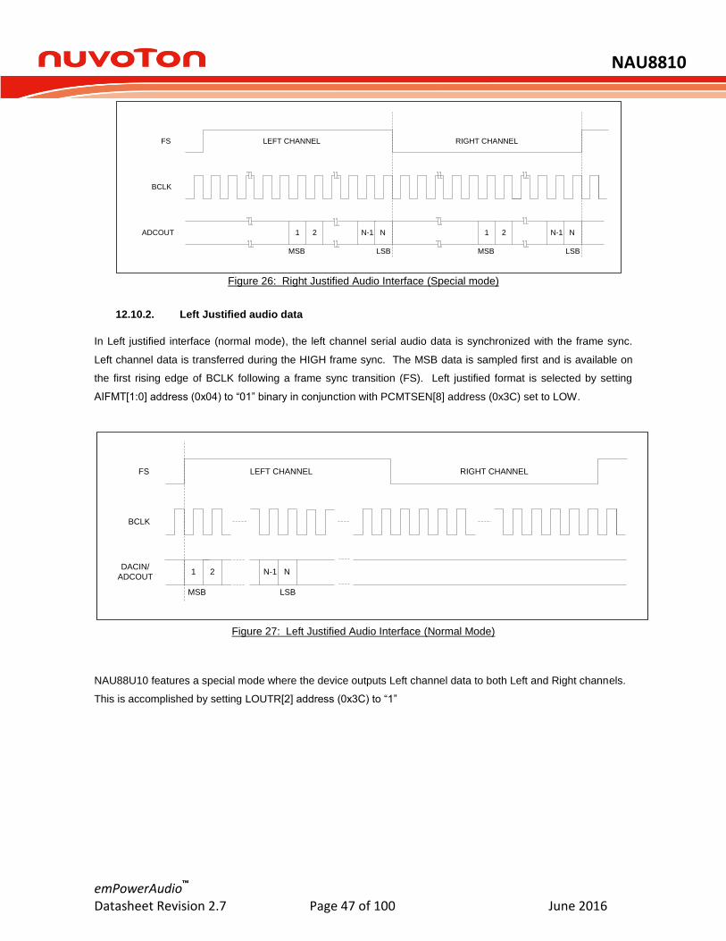
NAU8810
emPowerAudio™ Datasheet Revision 2.7 Page 47 of 100 June 2016
Figure 26: Right Justified Audio Interface (Special mode)
12.10.2. Left Justified audio data
In Left justified interface (normal mode), the left channel serial audio data is synchronized with the frame sync.
Left channel data is transferred during the HIGH frame sync. The MSB data is sampled first and is available on
the first rising edge of BCLK following a frame sync transition (FS). Left justified format is selected by setting
AIFMT[1:0] address (0x04) to “01” binary in conjunction with PCMTSEN[8] address (0x3C) set to LOW.
Figure 27: Left Justified Audio Interface (Normal Mode)
NAU88U10 features a special mode where the device outputs Left channel data to both Left and Right channels.
This is accomplished by setting LOUTR[2] address (0x3C) to “1”
LEFT CHANNEL RIGHT CHANNELFS
N-1 N1 2
MSB LSB
DACIN/
ADCOUT
BCLK
LEFT CHANNEL RIGHT CHANNELFS
N-1 N1 2
MSB LSB
ADCOUT
BCLK
N-1 N1 2
MSB LSB

NAU8810
emPowerAudio™ Datasheet Revision 2.7 Page 48 of 100 June 2016
Figure 28: Left Justified Audio Interface (Special mode)
12.10.3. I2S audio data
In I2S interface (normal mode), the left channel serial audio data is synchronized with the frame sync. Left
channel data is transferred during the LOW frame sync. The MSB data is sampled first. The data is latched on
the second rising edge of BCLK following a frame sync transition (FS). I2S format is selected by setting
AIFMT[1:0] address (0x04) to “10” binary in conjunction with PCMTSEN[8] address (0x3C) set to LOW.
Figure 29: I2S Audio Interface (Normal Mode) NAU88U10 features a special mode where the device outputs Left channel data to both Left and Right channels.
This is accomplished by setting LOUTR[2] address (0x3C) to “1”
LEFT CHANNEL RIGHT CHANNELFS
N-1 N1 2
MSB LSB
DACIN/
ADCOUT
BCLK
1 BCLK
LEFT CHANNEL RIGHT CHANNELFS
N-1 N1 2
MSB LSB
ADCOUT
BCLK
N-1 N1 2
MSB LSB

NAU8810
emPowerAudio™ Datasheet Revision 2.7 Page 49 of 100 June 2016
Figure 30: I2S Audio Interface (Special mode)
12.10.4. PCM audio data
In PCM interface (normal mode), the left channel serial audio data is synchronized with the frame sync. Left
channel data is transferred during the LOW frame sync. The MSB data is sampled first. The data is latched on
the second rising edge of BCLK following a frame sync transition (FS). PCM format is selected by setting
AIFMT[4:3] address (0x04) to “11” binary in conjunction with PCMTSEN[8] address (0x3C) set to LOW.
The digital data can be forced to appear on the right phase of the FS by setting ADCPHS[0] and DACPHS[1]
address (0x04) bits to HIGH respectively. The starting point of the right phase data depends on the word length
WLEN[6:5] address (0x04) after the frame sync transition (FS).
Figure 31: PCM Mode Audio Interface (Normal Mode) NAU88U10 features a special mode where the device outputs Left channel data to both Left and Right channels.
This is accomplished by setting LOUTR[2] address (0x3C) to “1”
LEFT CHANNELFS
N-1 N1 2
MSB LSB
DACIN/
ADCOUT
BCLK
1 BCLK
Word Length, WLEN[6:5]
LEFT CHANNEL RIGHT CHANNELFS
N-1 N1 2
MSB LSB
ADCOUT
BCLK
1 BCLK
N-1 N1 2
MSB LSB
1 BCLK

NAU8810
emPowerAudio™ Datasheet Revision 2.7 Page 50 of 100 June 2016
Figure 32: PCM Mode Audio Interface (Special mode)
12.10.5. PCM Time Slot audio data
In PCM Time-Slot interface (normal mode), the left channel serial audio data is synchronized with the frame sync.
Left channel data is transferred during the LOW frame sync. The MSB data is sampled first. The starting point of
the timeslot is controlled by a 10-bit byte TSLOT[9:0] address (0x3B and 0x3C). The data is latched on the first
rising edge of BCLK following a frame sync transition (FS) providing PCM is in timeslot zero (TSLOT[9:0] = 000).
PCM Time-Slot format is selected by setting AIFMT[4:3] address (0x04) to “11” binary in conjunction with
PCMTSEN[8] address (0x3C) set to HIGH. The digital data can be forced to appear on the right phase of the FS
by setting ADCPHS[0] and DACPHS[1] address (0x04) bits to HIGH respectively. The starting point of the right
phase data depends on the word length WLEN[6:5] address (0x04) and timeslot assignment TSLOT[9:0] address
(0x3B and 0x3C) after the frame sync transition (FS). DACIN will return to the bus condition either on the
negative edge of BCLK during the LSB, or on the positive edge of BCLK following the LSB depending on the
setting of TRI[7] address (0x3C). Tri-stating on the negative edge allows the transmission of data by multiple
sources in adjacent timeslots without the risk of driver contention.
Figure 33: PCM Time Slot Mode (Time slot = 0) (Normal Mode) NAU88U10 features a special mode where the device outputs Left channel data to both Left and Right channels.
This is accomplished by setting LOUTR[2] address (0x3C) to “1”
LEFT CHANNELFS
N-1 N1 2
MSB LSB
DACIN/
ADCOUT
BCLK
1 BCLK
Word Length, WLEN[6:5]
LEFT CHANNELFS
N-1 N1 2
MSB LSB
ADCOUT
BCLK
1 BCLK
Word Length, WLEN[6:5]
N-1 N1 2
MSB LSB
Word Length, WLEN[6:5]
RIGHT CHANNEL

NAU8810
emPowerAudio™ Datasheet Revision 2.7 Page 51 of 100 June 2016
Figure 34: PCM Time Slot Mode (Time slot = 0) (Special mode)
12.10.6. Companding
Companding is used in digital communication systems to optimize signal-to-noise ratios with reduced data bit
rates, and make use of non-linear algorithms. NAU88U10 supports two different types of companding A-law and
µ-law on both transmit and receive sides. A-law algorithm is used in European communication systems and µ-law
algorithm is used by North America, Japan, and Australia. This feature is enabled by setting DACCM[4:3]
address (0x05) or ADCCM[2:1] address (0x05) register bits. Companding converts 13 bits (µ -law) or 12 bits (A-
law) to 8 bits using non-linear quantization. The companded signal is an 8-bit word containing sign (1-bit),
exponent (3-bits) and mantissa (4-bits). As recommended by the G.711 standard (all 8-bits are inverted for µ-law,
all even data bits are inverted for A-law).
Setting CMB8[5] address 0x05 to 1 will cause the PCM interface to use 8-bit word length for data transfer,
overriding the word length configuration setting in WLEN[6:5] address 0x04.
Addr D8 D7 D6 D5 D4 D3 D2 D1 D0 Default
0x05 0 0 0 CMB8 DACCM[1:0] ADCCM[1:0] ADDAP 0x000
Table 26: Companding Control The following equations for data compression (as set out by ITU-T G.711 standard):
µ-law (where µ=255 for the U.S. and Japan):
F(x) = ln( 1 + µ|x|) / ln( 1 + µ) -1 ≤ x ≤ 1
A-law (where A=87.6 for Europe):
LEFT CHANNELFS
N-1 N1 2
MSB LSB
ADCOUT
BCLK
1 BCLK
Word Length, WLEN[6:5]
N-1 N1 2
MSB LSB
Word Length, WLEN[6:5]
RIGHT CHANNEL

NAU8810
emPowerAudio™ Datasheet Revision 2.7 Page 52 of 100 June 2016
12.11. POWER SUPPLY
This device has been designed to operate reliably using a wide range of power supply conditions and power-
on/power-off sequences. There are no special requirements for the sequence or rate at which the various power
supply pins change. Any supply can rise or fall at any time without harm to the device. However, pops and clicks
may result from some sequences. Optimum handling of hardware and software power-on and power-off
sequencing is described in more detail in the Power Up/Down Sequencing section of this document.
12.11.1. Power-On Reset
The NAU88U10 does not have an external reset pin. The device reset function is automatically generated
internally when power supplies are too low for reliable operation. The internal reset is generated any time that
either VDDA or VDDD is lower than is required for reliable maintenance of internal logic conditions. The threshold
voltage for VDDA is approximately ~1.52Vdc and the threshold voltage for VDDD is approximately
~0.67Vdc. Note that these are much lower voltages than are required for normal operation of the chip. These
values are mentioned here as general guidance as to overall system design.
If either VDDA or VDDD is below its respective threshold voltage, an internal reset condition may be
asserted. During this time, all registers and controls are set to the hardware determined initial
conditions. Software access during this time will be ignored, and any expected actions from software activity will
be invalid.
When both VDDA and VDDD reach a value above their respective thresholds, an internal reset pulse is generated
which extends the reset condition for an additional time. The duration of this extended reset time is approximately
50 microseconds, but not longer than 100 microseconds. The reset condition remains asserted during this
time. If either VDDA or VDDD at any time becomes lower than its respective threshold voltage, a new reset
condition will result. The reset condition will continue until both VDDA and VDDD again higher than their
respective thresholds. After VDDA and VDDD are again both greater than their respective threshold voltage, a
new reset pulse will be generated, which again will extend the reset condition for not longer than an additional 100
microseconds.
12.11.2. Power Related Software Considerations
There is no direct way for software to determine that the device is actively held in a reset condition. If there is a
possibility that software could be accessing the device sooner than 100 microseconds after the VDDA and VDDD
supplies are valid, the reset condition can be determined indirectly. This is accomplished by writing a value to any
register other than register 0x00, with that value being different than the power-on reset initial values. The
optimum choice of register for this purpose may be dependent on the system design, and it is recommended the
system engineer choose the register and register test bit for this purpose. After writing the value, software will
then back the same register. When the register test bit s back as the new value, instead of the power-on reset
initial value, software can reliably determine that the reset condition has ended.

NAU8810
emPowerAudio™ Datasheet Revision 2.7 Page 53 of 100 June 2016
Although it is not required, it is strongly recommended that a Software Reset command should be issued after
power-on and after the power-on-reset condition is ended. This will help insure reliable operation under every
power sequencing condition that could occur.
12.11.3. Software Reset
The control registers can be reset to default conditions by writing any value to RST address (0x00), using any of
the control interface modes. Writing valid data to any other register disables the reset, but all registers will need
to be initiated again appropriate to the operation. See the applications section on powering NAU88U10 up for
information on avoiding pops and clicks after a software reset.
12.11.4. Power Up/Down Sequencing
Most audio products have issues during power up and power down in the form of pop and click noise. To avoid
cuch issues the NAU88U10 provides four different power supplies VDDA, VDDD and VDDSPK with separated
grounds VSSA, VSSD and VSSSPK. The audio CODEC circuitry, the input amplifiers, output amplifiers and
drivers, the audio ADC and DAC converters, the PLL, and so on, can be powered up and down individually by
software control via 2-Wire interface. The zero cross function should be used when changing the volume in the
PGAs to avoid any audible pops or clicks. There are two different modes of operation 5.0V and 3.3V mode. The
recommended power-up and power-down sequences for both the modes are outlined as following.

NAU8810
emPowerAudio™ Datasheet Revision 2.7 Page 54 of 100 June 2016
Power Up
Name VDDSPK - 3.3V operation VDDSPK - 5.0V operation
Power supplies
Analog – VDDA Analog – VDDA
Digital – VDDD Digital – VDDD
Output driver - VDDSPK Output driver – VDDSPK
Mode SPKBST[2] = 0 SPKBST[2] = 1
MOUTBST[3] = 0 MOUTBST[3] = 1
Power Management
REFIMP[1:0] as required (value of the REFIMP bits based on the startup time which is a combination of the reference impedance and the decoupling capacitor on VREF)
ABIASEN[3] = 1 (enables the internal device bias for all analog blocks)
IOBUFEN[2] = 1 (enables the internal device bias buffer)
Clock divider
CLKIOEN[0] if required CLKIOEN[0] if required
BCLKSEL[4:2] if required BCLKSEL[4:2] if required
MCLKSEL[7:5] if required MCLKSEL[7:5] if required
PLL PLLEN[5] if required PLLEN[5] if required
DAC, ADC DACEN[0] = 1 DACEN[0] = 1
ADCEN[0] = 1 ADCEN[0] = 1
Mixers SPKMXEN[2] SPKMXEN[2]
MOUTMXEN[3] MOUTMXEN[3]
Output stages
MOUTEN[7] MOUTEN[7]
NSPKEN[6] NSPKEN[6]
PSPKEN[5] PSPKEN[5]
Un-mute DAC DACMT[6] = 0 DACMT[6] = 0
Table 27: Power up sequence
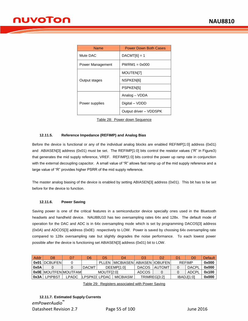
NAU8810
emPowerAudio™ Datasheet Revision 2.7 Page 55 of 100 June 2016
Name Power Down Both Cases
Mute DAC DACMT[6] = 1
Power Management PWRM1 = 0x000
Output stages
MOUTEN[7]
NSPKEN[6]
PSPKEN[5]
Power supplies
Analog – VDDA
Digital – VDDD
Output driver – VDDSPK
Table 28: Power down Sequence
12.11.5. Reference Impedance (REFIMP) and Analog Bias
Before the device is functional or any of the individual analog blocks are enabled REFIMP[1:0] address (0x01)
and ABIASEN[3] address (0x01) must be set. The REFIMP[1:0] bits control the resistor values (“R” in Figure3)
that generates the mid supply reference, VREF. REFIMP[1:0] bits control the power up ramp rate in conjunction
with the external decoupling capacitor. A small value of “R” allows fast ramp up of the mid supply reference and a
large value of “R” provides higher PSRR of the mid supply reference.
The master analog biasing of the device is enabled by setting ABIASEN[3] address (0x01). This bit has to be set
before for the device to function.
12.11.6. Power Saving
Saving power is one of the critical features in a semiconductor device specially ones used in the Bluetooth
headsets and handheld device. NAU88U10 has two oversampling rates 64x and 128x. The default mode of
operation for the DAC and ADC is in 64x oversampling mode which is set by programming DACOS[3] address
(0x0A) and ADCOS[3] address (0x0E) respectively to LOW. Power is saved by choosing 64x oversampling rate
compared to 128x oversampling rate but slightly degrades the noise performance. To each lowest power
possible after the device is functioning set ABIASEN[3] address (0x01) bit to LOW.
Addr D8 D7 D6 D5 D4 D3 D2 D1 D0 Default
0x01 DCBUFEN 0 PLLEN MICBIASEN ABIASEN IOBUFEN REFIMP 0x000
0x0A 0 0 DACMT DEEMP[1:0] DACOS AUTOMT 0 DACPL 0x000
0x0E MOUTFEN MOUTFAM MOUTF[2:0] ADCOS 0 0 ADCPL 0x100
0x3A LPIPBST LPADC LPSPKD LPDAC MICBIASM TRIMREG[3:2] IBADJ[1:0] 0x000
Table 29: Registers associated with Power Saving
12.11.7. Estimated Supply Currents

NAU8810
emPowerAudio™ Datasheet Revision 2.7 Page 56 of 100 June 2016
NAU88U10 can be programmed to enable or disable various analog blocks individually. The table below shows
the amount of current consumed by certain analog blocks. Sample rate settings will vary current consumption of
the VDDD supply. VDDD consumes approximately 4mA with VDDD = 1.8V and fs = 48kHz. Lower sampling
rates will draw lower current.
BIT Address VDDA CURRENT
REFIMP[1:0]
0x01
10K => 300 uA 161k/595k < 100 uA
IOBUFEN[2] 40uA
ABIASEN[3] 600uA
MICBIASEN[4] 500 uA
PLLEN[5] 2.5mA Clocks Applied
DCBUFEN[8] 80uA
ADCEN[0]
0x02
x64 - ADCOS= 0 => 2.0mA x128 – ADCOS= 1 => 3.0mA
PGAEN[2] 400uA
BSTEN[4] 200 uA
DACEN[0]
0x03
X64 (DACOS=0)=>1.6mA x128(DACOS=1)=>1.7mA
SPKMXEN[2] 400uA
MOUTMXEN[3] 200uA
NSPKEN[6] 1mA from VDDSPK + 100uA (VDDA = 5V mode)
PSPKEN[5] 1mA from VDDSPK + 100uA (VDDA = 5V mode)
MOUTEN[7] 100uA
Table 30: VDDA 3.3V Supply Current

NAU8810
emPowerAudio™ Datasheet Revision 2.7 Page 57 of 100 June 2016
13. REGISTER DESCRIPTION
Register Address
Register Names Register Bits
Default
DEC HEX D8 D7 D6 D5 D4 D3 D2 D1 D0
0 0 Software Reset RESET (SOFTWARE) 000
POWER MANAGEMENT
1 01 Power Management 1 DCBUFEN 0 0 PLLEN MICBIASEN ABIASEN IOBUFEN REFIMP 000
2 02 Power Management 2 0 0 0 0 BSTEN 0 PGAEN 0 ADCEN 000
3 03 Power Management 3 0 MOUTEN NSPKEN PSPKEN 0 MOUTMXEN SPKMXEN 0 DACEN 000
AUDIO CONTROL
4 04 Audio Interface BCLKP FSP WLEN[1:0] AIFMT[1:0] DACPHS ADCPHS 0 050
5 05 Companding 0 0 0 0 DACCM[1:0] ADCCM[1:0] ADDAP 000
6 06 Clock Control 1 CLKM MCLKSEL[2:0] BCLKSEL[2:0] 0 CLKIOEN 140
7 07 Clock Control 2 0 0 0 0 0 SMPLR[2:0] SCLKEN 000
10 0A DAC CTRL 0 0 DACMT DEEMP[1:0] DACOS AUTOMT 0 DACPL 000
11 0B DAC Volume 0 DACGAIN 0FF
14 0E ADC CTRL HPFEN HPFAM HPF[2:0] ADCOS 0 0 ADCPL 100
15 0F ADC Volume 0 ADCGAIN 0FF
EQUALISER
18 0x12 EQ1-Low Cutoff EQM 0 EQ1CF[1:0] EQ1GC[4:0] 12C
19 0x13 EQ2-Peak 1 EQ2BW 0 EQ2CF[1:0] EQ2GC[4:0] 02C
20 0x14 EQ3-Peak 2 EQ3BW 0 EQ3CF[1:0] EQ3GC[4:0] 02C
21 0x15 EQ4-Peak3 EQ4BW 0 EQ4CF[1:0] EQ4GC[4:0] 02C
22 0x16 EQ5-High Cutoff 0 0 EQ5CF[1:0] EQ5GC[4:0] 02C
DIGITAL TO ANALOG (DAC) LIMITER
24 18 DAC Limiter 1 DACLIMEN DACLIMDCY[3:0] DACLIMATK[3:0] 032
25 19 DAC Limiter 2 0 0 DACLIMTHL[2:0] DACLIMBST[3:0] 000
NOTCH FILTER
27 1B Notch Filter High NFCU NFCEN NFCA0[13:7] 000
28 1C Notch Filter Low NFCU 0 NFCA0[6:0] 000
29 1D Notch Filter High NFCU 0 NFCA1[13:7] 000
30 1E Notch Filter Low NFCU 0 NFCA1[6:0] 000
ALC CONTROL
32 20 ALC CTRL 1 ALCEN 0 0 ALCMXGAIN[2:0] ALCMNGAIN[2:0] 038
33 21 ALC CTRL 2 ALCZC ALCHT[3:0] ALCSL[3:0] 00B
34 22 ALC CTRL 3 ALCM ALCDCY[3:0] ALCATK[3:0] 032
35 23 Noise Gate 0 0 0 0 0 ALCNEN ALCNTH[2:0] 000
PLL CONTROL
36 24 PLL N CTRL 0 0 0 0 PLLMCLK PLLN[3:0] 008
37 25 PLL K 1 0 0 0 PLLK[23:18] 00C
38 26 PLL K 2 PLLK[17:9] 093

NAU8810
emPowerAudio™ Datasheet Revision 2.7 Page 58 of 100 June 2016
Register Address
Register Names Register Bits
Default
DEC HEX D8 D7 D6 D5 D4 D3 D2 D1 D0
39 27 PLL K 3 PLLK[8:0] 0E9
INPUT, OUTPUT & MIXER CONTROL
40 28 Attenuation CTRL 0 0 0 0 0 0 MOUTATT SPKATT 0 000
44 2C Input CTRL MICBIASV 0 0 0 0 0 NMICPGA PMICPGA 003
45 2D PGA Gain 0 PGAZC PGAMT PGAGAIN[5:0] 010
47 2F ADC Boost PGABST 0 PMICBSTGAIN 0 0 0 0 100
49 31 Output CTRL 0 0 0 0 0 MOUTBST SPKBST TSEN AOUTIMP 002
50 32 Mixer CTRL 0 0 0 0 0 0 0 BYPSPK DACSPK 001
54 36 SPKOUT Volume 0 SPKZC SPKMT SPKGAIN[5:0] 039
56 38 MONO Mixer Control 0 0 MOUTMT 0 0 0 0 BYPMOUT DACMOUT 001
LOW POWER CONTROL
58 3A Power Management 4 LPIPBST LPADC LPSPKD LPDAC MICBIASM TRIMREG IBADJ 000
PCM TIME SLOT & ADCOUT IMPEDANCE OPTION CONTROL
59 3B Time Slot TSLOT[8:0] 000
60 3C ADCOUT Drive PCMTSEN TRI PCM8BIT PUDOEN PUDPE PUDPS LOUTR PCMB TSLOT[9:8] 020
REGISTER ID
62 3E Silicon Revision 0 1 1 1 0 1 1 1 1 0EF
63 3F 2-Wire ID 0 0 0 0 1 1 0 1 0 01A
64 40 Additional ID 0 1 1 0 0 1 0 1 0 0CA
65 41 Reserved 1 0 0 1 0 0 1 0 0 124
69 45 High Voltage CTRL 0 0 0 0 MOUTMT 0 HVOPU 0 HVOP 001
70 46 ALC Enhancements 1 ALCTBLSEL ALCPKSEL ALCNGSEL ALCGAINL ( ONLY) 000
71 47 ALC Enhancements 2 PKLIMEN 0 0 1 1 1 0 0 1 039
73 49 Additional IF CTRL 0 FSERRVAL[1:0] FSERFLSH FSERRENA NFDLY DACINMT PLLLOCKP DACOS256 000
75 4B Power/Tie-off CTRL 0 LPSPKA 0 0 0 0 MANVREFH MANVREFM MANVREFL 000
76 4C AGC P2P Detector P2PDET ( ONLY) 000
77 4D AGC Peak Detector PDET ( ONLY) 000
78 4E Control and Status 0 0 AMTCTRL HVDET NSGATE AMUTE DMUTE 0 FTDEC 000
79 4F Output tie-off CTRL MANOUTEN SBUFH SBUFL SNSPK SPSPK SMOUT 0 0 0 000

NAU8810
emPowerAudio™ Datasheet Revision 2.7 Page 59 of 100 June 2016
13.1. SOFTWARE RESET
Addr D8 D7 D6 D5 D4 D3 D2 D1 D0 Default
0x00 RESET (SOFTWARE) 0x000
This is device Reset register. Performing a write instruction to this register with any data will reset all the bits in the register map to default.
13.2. POWER MANAGEMENT REGISTERS
13.2.1. Power Management 1
Addr D8 D7 D6 D5 D4 D3 D2 D1 D0 Default
0x01 DCBUFEN 0 0 PLLEN MICBIASEN ABIASEN IOBUFEN REFIMP[1:0] 0x000
Name Buffer for DC level shifting
Enable PLL enable
Microphone Bias
Enable
Analogue amplifier
bias control
Unused input/output tie
off buffer enable
Bit DCBUFEN[8] PLLEN[5] MICBIASEN[4] ABIASEN[3] IOBUFEN[2]
0 Disable Disable Disable Disable Disable
1 Enable
(required for 1.5x gain)
Enable Enable Enable Enable
The DCBUFEN[8] address (0x01) is a dedicated buffer for DC level shifting output stages when in 1.5x gain boost configuration. There are three different reference impedance selections to choose from as follows:
VREF REFERENCE IMPEDANCE SELECTION
(“R” refers to “R” as shown in Figure3)
REFIMP[1] REFIMP[0] Mode
0 0 Disable
0 1 R = 80 k
1 0 R = 300 k
1 1 R = 3 k

NAU8810
emPowerAudio™ Datasheet Revision 2.7 Page 60 of 100 June 2016
13.2.2. Power Management 2
Addr D8 D7 D6 D5 D4 D3 D2 D1 D0 Default
0x02 0 0 0 0 BSTEN 0 PGAEN 0 ADCEN 0x000
Name Input Boost
Enable MIC(+/-)
PGA Enable ADC Enable
Bit BSTEN[4] PGAEN[2] ADCEN[0]
0 Stage Disable Disable Disable
1 Stage Enable Enable Enable
13.2.3. Power Management 3
Addr D8 D7 D6 D5 D4 D3 D2 D1 D0 Default
0x03 0 MOUTEN NSPKEN PSPKEN BIASGEN MOUTMXEN SPKMXEN 0 DACEN 0x000
Name MOUT Enable
SPKOUT- Enable
SPKOUT+ Enable
Bias Enable MONO Mixer
Enable Speaker
Mixer Enable DAC
Enable
Bit MOUTEN[7] NSPKEN[6] PSPKEN[5] BIASGEN[4] MOUTMXEN[3] SPKMXEN[2] DACEN[0]
0 Disable Disable Disable Disable Disable Disable Disable
1 Enable Enable Enable Enable Enable Enable Enable
13.3. AUDIO CONTROL REGISTERS
13.3.1. Audio Interface Control
Addr D8 D7 D6 D5 D4 D3 D2 D1 D0 Default
0x04 BCLKP FSP WLEN[1:0] AIFMT[1:0] DACPHS ADCPHS 0 0x050
The following table explains the PCM control register bits.
Name BCLK
Polarity Frame Clock
Polarity
DAC Data ‘right’ or ‘left’
phases of FRAME clock
ADC Data ‘right’ or ‘left’
phases of FRAME clock
Bit BCLKP[8] FSP[7] DACPHS[2] ADCPHS[1]
0 Normal Normal DAC data appear in ‘left’ phase of FRAME
ADC data appear in ‘left’ phase of FRAME
1 Inverted Inverted DAC data appears in ‘right’ phase of FRAME
ADC data appears in ‘right’ phase of FRAME
There are three different CODEC modes to choose from as follows:

NAU8810
emPowerAudio™ Datasheet Revision 2.7 Page 61 of 100 June 2016
Word Length Selection Audio Data Format Select
WLEN[6] WLEN[5] Bits AIFMT[4] AIFMT[3] Format
0 0 16 0 0 Right
Justified
0 1 20 0 1 Left Justified
1 0 24 1 0 I2S
1 1 32 1 1 PCM A
13.3.2. Audio Interface Companding Control
Addr D8 D7 D6 D5 D4 D3 D2 D1 D0 Default
0x05 0 0 0 CMB8 DACCM[1:0] ADCCM[1:0] ADDAP 0x000
The NAU88U10 provides a Digital Loopback ADDAP[0] address (0x05) bit. Setting ADDAP[0] bit to HIGH enables the loopback so that the ADC data can be fed directly into the DAC input.
Companding Mode 8-bit word enable
DAC Companding Selection
ADC Companding Select
CMB8[5] Mode DACCM[4] DACCM[3] Mode ADCCM[2] ADCCM[1] Mode
0 normal operation
0 0 Disabled 0 0 Disabled
1 8-bit operation 0 1 Reserved 0 1 Reserved
1 0 µ-Law 1 0 µ-Law
1 1 A-Law 1 1 A-Law

NAU8810
emPowerAudio™ Datasheet Revision 2.7 Page 62 of 100 June 2016
13.3.3. Clock Control Register
Addr D8 D7 D6 D5 D4 D3 D2 D1 D0 Default
0x06 CLKM MCLKSEL[2:0] BCLKSEL[2:0] 0 CLKIOEN 0x140
Master Clock Selection Bit Clock Select
MCLKSEL [7]
MCLKSEL [6]
MCLKSEL [5]
Mode BCLKSEL
[4] BCLKSEL
[3] BCLKSEL
[2] Mode
0 0 0 1
0 0 0 1
(BCLK=MCLK)
0 0 1 1.5
0 0 1 2
(BCLK=MCLK/2)
0 1 0 2 0 1 0 4
0 1 1 3 0 1 1 8
1 0 0 4 1 0 0 16
1 0 1 6 1 0 1 32
1 1 0 8 1 1 0 Reserved
1 1 1 12 1 1 1 Reserved
Name Source of Internal Clock FRAME and BCLK
Bit CLKM[8] CLKIOEN[0]
0 MCLK (PLL Bypassed) Slave Mode
1 MCLK (PLL Output) Master Mode

NAU8810
emPowerAudio™ Datasheet Revision 2.7 Page 63 of 100 June 2016
13.3.4. Audio Sample Rate Control Register
Addr D8 D7 D6 D5 D4 D3 D2 D1 D0 Default
0x07 0 0 0 0 0 SMPLR[2:0] SCLKEN 0x000
The Audio sample rate configures only the coefficients for the internal digital filters to match the actual sample rate. It does not in any way actually set or change the ADC or DAC audio sample rate.
Sample Rate Selection
SMPLR[3] SMPLR[2] SMPLR[1] Mode (Hz)
0 0 0 48 k
0 0 1 32 k
0 1 0 24 k
0 1 1 16 k
1 0 0 12 k
1 0 1 8 k
1 1 0 Reserved
1 1 1 Reserved
NAU88U10 provides a slow clock to be used for the zero cross timeout.
Bit Slow Clock Enable
SCLKEN[0]
0 MCLK
1 PLL Output (Period 221
* MCLK)
13.3.5. DAC Control Register
Addr D8 D7 D6 D5 D4 D3 D2 D1 D0 Default
0x0A 0 0 DACMT DEEMP[1:0] DACOS AUTOMT 0 DACPL 0x000
Name Soft Mute Enable Over Sample Rate Auto Mute enable Polarity Invert
Bit DACMT[6] DACOS[3] AUTOMT[2] DACPL[0]
0 Disable 64x
(Lowest power) Disable Normal
1 Enable 128x
(best SNR) Enable
DAC Output
Inverted

NAU8810
emPowerAudio™ Datasheet Revision 2.7 Page 64 of 100 June 2016
De-emphasis
DEEMP[5] DEEMP[4] Mode
0 0 No de-emphasis
0 1 32kHz sample rate
1 0 44.1kHz sample rate
1 1 48kHz sample rate
13.3.6. DAC Gain Control Register
Addr D8 D7 D6 D5 D4 D3 D2 D1 D0 Default
0x0B 0 DACGAIN 0x0FF
DAC Gain
DACGAIN[7:0] Mode (dB)
B7 B6 B5 B4 B3 B2 B1 B0
0 0 0 0 0 0 0 0 Digital Mute
0 0 0 0 0 0 0 1 -127.0
0 0 0 0 0 0 1 0 -126.5
0 0 0 0 0 0 1 1 -126.0
DAC Gain Range -127dB to 0dB @ 0.5 increments
1 1 1 1 1 1 0 0 -1.5
1 1 1 1 1 1 0 1 -1.0
1 1 1 1 1 1 1 0 -0.5
1 1 1 1 1 1 1 1 0.0
13.3.7. ADC Control Register
Addr D8 D7 D6 D5 D4 D3 D2 D1 D0 Default
0x0E HPFEN HPFAM HPF[2:0] ADCOS 0 0 ADCPL 0x100
Name High Pass Filter
Enable
Audio or Application
Mode
Over Sample
Rate ADC Polarity
Bit HPFEN[8] HPFAM[7] ADCOS[3] ADCPL[0]
0 Disable Audio (1st order, fc ~ 3.7 Hz) 64x (Lowest power) Normal
1 Enable Application (2nd
order, fc = HPF) 128x (best SNR) Inverted

NAU8810
emPowerAudio™ Datasheet Revision 2.7 Page 65 of 100 June 2016
High Pass Filter fs ( kHz)
HPF[6] HPF[5] HPF[4] SMPLR=101 SMPLR=100
SMPLR=011 SMPLR=010
SMPLR=001 SMPLR=000
B2 B1 B0 8 11.025 12 16 22.05 24 32 44.1 48
0 0 0 82 113 122 82 113 122 82 113 122
0 0 1 102 141 153 102 141 153 102 141 153
0 1 0 131 180 156 131 180 156 131 180 156
0 1 1 163 225 245 163 225 245 163 225 245
1 0 0 204 281 306 204 281 306 204 281 306
1 0 1 261 360 392 261 360 392 261 360 392
1 1 0 327 450 490 327 450 490 327 450 490
1 1 1 408 563 612 408 563 612 408 563 612
13.3.8. ADC Gain Control Register
Addr D8 D7 D6 D5 D4 D3 D2 D1 D0 Default
0x0F 0 ADCGAIN 0x0FF
ADC Gain
ADCGAIN[7:0] Mode (dB)
B7 B6 B5 B4 B3 B2 B1 B0
0 0 0 0 0 0 0 0 Unused
0 0 0 0 0 0 0 1 -127.0
0 0 0 0 0 0 1 0 -126.5
0 0 0 0 0 0 1 1 -126.0
ADC Gain Range -127dB to 0dB @ 0.5 increments
1 1 1 1 1 1 0 0 -1.5
1 1 1 1 1 1 0 1 -1.0
1 1 1 1 1 1 1 0 -0.5
1 1 1 1 1 1 1 1 0.0

NAU8810
emPowerAudio™ Datasheet Revision 2.7 Page 66 of 100 June 2016
13.4. 5-BAND EQUALIZER CONTROL REGISTERS
Address D8 D7 D6 D5 D4 D3 D2 D1 D0 Default
0x12 EQM 0 EQ1CF[1:0] EQ1GC[4:0] 0x12C
0x13 EQ2BW 0 EQ2CF[1:0] EQ2GC[4:0] 0x02C
0x14 EQ3BW 0 EQ3CF[1:0] EQ3GC[4:0] 0x 02C
0x15 EQ4BW 0 EQ4CF[1:0] EQ4GC[4:0] 0x02C
0x16 0 0 EQ5CF[1:0] EQ5GC[4:0] 0x02C
Equalizer Gain
EQ1GC, EQ2GC, EQ3GC, EQ4GC, EQ5GC [4:0] Mode (dB)
B4 B3 B2 B1 B0
0 0 0 0 0 +12
0 0 0 0 1 +11
::: ::: ::: ::: ::: :::
0 1 0 1 1 +1
0 1 1 0 0 0
0 1 1 0 1 -1
Equalizer Gain Range -12dB to +12dB @ 1.0 increment
::: ::: ::: ::: ::: :::
1 0 1 1 1 -11
1 1 0 0 0 -12
1 1 0 0 1
Reserved To
1 1 1 1 1
Center Frequencies
B1 B0 EQ2CF[6:5] EQ3CF[6:5] EQ4CF[6:5]
0 0 230 650 1.8 k
0 1 300 850 2.4 k
1 0 385 1.1 k 3.2 k
1 1 500 1.4 k 4.1 k

NAU8810
emPowerAudio™ Datasheet Revision 2.7 Page 67 of 100 June 2016
Cut-off Frequencies
B1 B0 EQ1CF[6:5] EQ5CF[6:5
]
0 0 80 5.3 k
0 1 105 6.9 k
1 0 135 9.0 k
1 1 175 11.7 k
Bit Bandwidth Control Equalizer Path
EQ2BW – EQ4BW EQM[8]
0 Narrow bandwidth ADC path
1 Wide bandwidth DAC path
13.5. DIGITAL TO ANALOG CONVERTER (DAC) LIMITER REGISTERS
Addr D8 D7 D6 D5 D4 D3 D2 D1 D0 Default
0x18 DACLIMEN DACLIMDCY[3:0] DACLIMATK[3:0] 0x032
0x19 0 0 DACLIMTHL[2:0] DACLIMBST[3:0] 0x000
DAC Limiter Decay time (per 6dB gain change) for 44.1 kHz sampling. Note that these will scale with sample
rate
DAC Limiter Attack time (per 6dB gain change) for 44.1 kHz sampling. Note that these will scale with sample rate
DACLIMDCY[3:0] DACLIMATK[3:0]
B3 B2 B1 B0 Decay Time B3 B2 B1 B0 Attack Time
0 0 0 0 544.0 us 0 0 0 0 68 us
0 0 0 1 1.1 ms 0 0 0 1 136 us
0 0 1 0 2.2 ms 0 0 1 0 272 us
0 0 1 1 4.4 ms 0 0 1 1 544 us
0 1 0 0 8.7 ms 0 1 0 0 1.1 ms
0 1 0 1 17.4 ms 0 1 0 1 2.2 ms
0 1 1 0 35.0 ms 0 1 1 0 4.4 ms
0 1 1 1 69.6 ms 0 1 1 1 8.7 ms
1 0 0 0 139.0 ms 1 0 0 0 17.4 ms
1 0 0 1 278.5 ms 1 0 0 1 35 ms
1 0 1 0 557.0 ms 1 0 1 0 69.6 ms
1 0 1 1
1.1 s
1 0 1 1
139 ms To To
1 1 1 1 1 1 1 1

NAU8810
emPowerAudio™ Datasheet Revision 2.7 Page 68 of 100 June 2016
DAC Limiter Programmable signal threshold level (determines level at which the limiter starts to
operate)
DAC Limiter volume Boost (can be used as a
stand alone volume Boost when DACLIMEN=0)
DACLIMTHL[3:0] Threshold (dB)
DACLIMBST[3:0] Boost (dB) B2 B1 B0 B3 B2 B1 B0
0 0 0 -1 0 0 0 0 0
0 0 1 -2 0 0 0 1 +1
0 1 0 -3 0 0 1 0 +2
0 1 1 -4 0 0 1 1 +3
1 0 0 -5 0 1 0 0 +4
1 0 1
-6
0 1 0 1 +5
To 0 1 1 0 +6
1 1 1 0 1 1 1 +7
1 0 0 0 +8
1 0 0 1 +9
DAC Digital Limiter 1 0 1 0 +10
Bit DACLIMEN[8] 1 0 1 1 +11
0 Disabled 1 1 0 0 +12
1 Enabled 1 1 0 1
Reserved To
1 1 1 1
13.6. NOTCH FILTER REGISTERS
Addr D8 D7 D6 D5 D4 D3 D2 D1 D0 Default
0x1B NFCU NFCEN NFCA0[13:7] 0x000
0x1C NFCU 0 NFCA0[6:0] 0x000
0x1D NFCU 0 NFCA1[13:7] 0x000
0x1E NFCU 0 NFCA1[6:0] 0x000
The Notch Filter is enabled by setting NFCEN[7] address (0x1B) bit to HIGH. The coefficients, A0 and A1, should
be converted to 2’s complement numbers to determine the register values. A0 and A1 are represented by the
register bits NFCA0[13:0] and NFCA1[13:0]. Since there are four register of coefficients, a Notch Filter Update bit
is provided so that the coefficients can be updated simultaneously. NFCU[8] is provided in all registers of the
Notch Filter coefficients but only one bit needs to be toggled for LOW – HIGH – LOW for an update. If any of the
NFCU[8] bits are left HIGH then the Notch Filter coefficients will continuously update. An example of how to
calculate is provided in the Notch Filter section.

NAU8810
emPowerAudio™ Datasheet Revision 2.7 Page 69 of 100 June 2016
Name A0 A1 Notation Register Value (DEC)
Coefficient
s
b
s
b
f
f
f
f
2
2tan1
2
2tan1
s
c
f
fxA
2cos1 0
fc = center frequency (Hz) fb = -3dB bandwidth (Hz) fs = sample frequency (Hz)
NFCA0 = -A0 x 213
NFCA1 = -A1 x 2
12
(then convert to 2’s complement)
13.7. AUTOMATIC LEVEL CONTROL REGISTER
13.7.1. ALC1 REGISTER
Addr D8 D7 D6 D5 D4 D3 D2 D1 D0 Default
0x20 ALCEN 0 0 ALCMXGAIN[2:0] ALCMNGAIN[2:0] 0x038
Maximum Gain Minimum Gain
ALCMXGAIN[2:0] Mode
ALCMNGAIN[2:0] Mode
B2 B1 B0 B2 B1 B0
0 0 0 -6.75dB 0 0 0 -12dB
0 0 1 -0.75dB 0 0 1 -6dB
0 1 0 +5.25dB 0 1 0 0dB
0 1 1 +11.25dB 0 1 1 +6dB
1 0 0 +17.25dB 1 0 0 +12dB
1 0 1 +23.25dB 1 0 1 +18dB
1 1 0 +29.25dB 1 1 0 +24dB
1 1 1 +35.25dB 1 1 1 +30dB
Name ALC Enable
Bit ALCEN[8]
0 Disabled (PGA gain set by PGAGAIN register bits)
1 Enabled (ALC controls PGA gain)

NAU8810
emPowerAudio™ Datasheet Revision 2.7 Page 70 of 100 June 2016
13.7.2. ALC2 REGISTER
Addr D8 D7 D6 D5 D4 D3 D2 D1 D0 Default
0x21 ALCZC ALCHT[3:0] ALCSL[3:0] 0x00B
ALC HOLD TIME before gain is increased. ALC TARGET – sets signal level at ADC input
ALCHT[3:0] ALC Hold Time (sec)
ALCSL[3:0] ALC Target Level (dB) B7 B6 B5 B4 B3 B2 B1 B0
0 0 0 0 0 0 0 0 0 -28.5 fs
0 0 0 1 2 ms 0 0 0 1 -27 fs
0 0 1 0 4 ms 0 0 1 0 25.5 fs
Time Doubles with every increment ALC Target Level Range
-28.5dB to -6dB @ 1.5dB increments
1 0 0 0 256 ms 1 0 1 1 -12 fs
1 0 0 1 512 ms 1 1 0 0 -10.5 fs
1 0 1 0
1 s
1 1 0 1 -9 fs
To 1 1 1 0 -7.5 fs
1 1 1 1 1 1 1 1 -6 fs
Name ALC Zero Crossing
Detect
Bit ALCZC[8]
0 Disabled
1 Enabled
It is recommended that zero crossing should not be used in conjunction with the ALC or Limiter functions
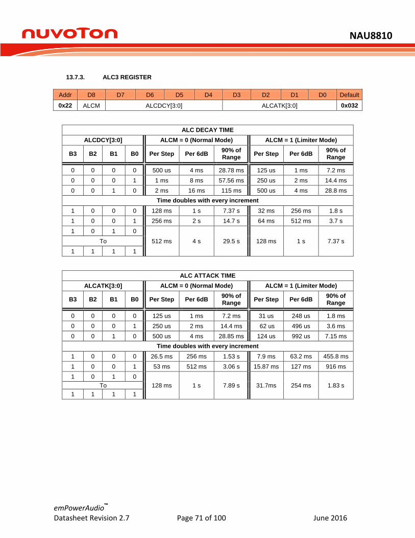
NAU8810
emPowerAudio™ Datasheet Revision 2.7 Page 71 of 100 June 2016
13.7.3. ALC3 REGISTER
Addr D8 D7 D6 D5 D4 D3 D2 D1 D0 Default
0x22 ALCM ALCDCY[3:0] ALCATK[3:0] 0x032
ALC DECAY TIME
ALCDCY[3:0] ALCM = 0 (Normal Mode) ALCM = 1 (Limiter Mode)
B3 B2 B1 B0 Per Step Per 6dB 90% of Range
Per Step Per 6dB 90% of Range
0 0 0 0 500 us 4 ms 28.78 ms 125 us 1 ms 7.2 ms
0 0 0 1 1 ms 8 ms 57.56 ms 250 us 2 ms 14.4 ms
0 0 1 0 2 ms 16 ms 115 ms 500 us 4 ms 28.8 ms
Time doubles with every increment
1 0 0 0 128 ms 1 s 7.37 s 32 ms 256 ms 1.8 s
1 0 0 1 256 ms 2 s 14.7 s 64 ms 512 ms 3.7 s
1 0 1 0
512 ms 4 s 29.5 s 128 ms 1 s 7.37 s To
1 1 1 1
ALC ATTACK TIME
ALCATK[3:0] ALCM = 0 (Normal Mode) ALCM = 1 (Limiter Mode)
B3 B2 B1 B0 Per Step Per 6dB 90% of Range
Per Step Per 6dB 90% of Range
0 0 0 0 125 us 1 ms 7.2 ms 31 us 248 us 1.8 ms
0 0 0 1 250 us 2 ms 14.4 ms 62 us 496 us 3.6 ms
0 0 1 0 500 us 4 ms 28.85 ms 124 us 992 us 7.15 ms
Time doubles with every increment
1 0 0 0 26.5 ms 256 ms 1.53 s 7.9 ms 63.2 ms 455.8 ms
1 0 0 1 53 ms 512 ms 3.06 s 15.87 ms 127 ms 916 ms
1 0 1 0
128 ms 1 s 7.89 s 31.7ms 254 ms 1.83 s To
1 1 1 1
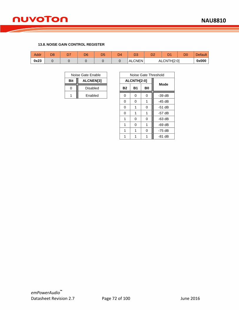
NAU8810
emPowerAudio™ Datasheet Revision 2.7 Page 72 of 100 June 2016
13.8. NOISE GAIN CONTROL REGISTER
Addr D8 D7 D6 D5 D4 D3 D2 D1 D0 Default
0x23 0 0 0 0 0 ALCNEN ALCNTH[2:0] 0x000
Noise Gate Enable Noise Gate Threshold
Bit ALCNEN[3] ALCNTH[2:0] Mode
0 Disabled B2 B1 B0
1 Enabled 0 0 0 -39 dB
0 0 1 -45 dB
0 1 0 -51 dB
0 1 1 -57 dB
1 0 0 -63 dB
1 0 1 -69 dB
1 1 0 -75 dB
1 1 1 -81 dB

NAU8810
emPowerAudio™ Datasheet Revision 2.7 Page 73 of 100 June 2016
13.9. PHASE LOCK LOOP (PLL) REGISTERS
13.9.1. PLL Control Registers
Addr D8 D7 D6 D5 D4 D3 D2 D1 D0 Default
0x24 0 0 0 0 PLLMCLK PLLN[3:0] 0x008
PLL Integer PLL Clock
PLLN[3:0] Frequency
Ratio
Bit PLLMCLK[4]
B3 B2 B1 B0 0 MCLK not divided
0 0 0 1
Not Valid
1 Divide MCLK by 2 before input PLL
To
0 1 0 0
0 1 0 1 5
0 1 1 0 6
0 1 1 1 7
1 0 0 0 8
1 0 0 1 9
1 0 1 0 10
1 0 1 1 11
1 1 0 0 12
1 1 0 1 13
1 1 1 0 Not Valid
1 1 1 1
13.9.2. Phase Lock Loop Control (PLL) Registers
Addr D8 D7 D6 D5 D4 D3 D2 D1 D0 Default
0x25 0 0 0 PLLK[23:18] 0x00C
0x26 PLLK[17:9] 0x093
0x27 PLLK[8:0] 0x0E9
Fractional (K) part of PLLK1 – PLLK3 input/output frequency ratio

NAU8810
emPowerAudio™ Datasheet Revision 2.7 Page 74 of 100 June 2016
13.10. INPUT, OUTPUT, AND MIXERS CONTROL REGISTER
13.10.1. Attenuation Control Register
Addr D8 D7 D6 D5 D4 D3 D2 D1 D0 Default
0x28 0 0 0 0 0 0 MOUTATT SPKATT 0 0x000
Attenuation Control
Name Attenuation control for bypass path (output of input boost stage) to speaker mixer and MONO
mixer input
Bit MOUTATT[2] SPKATT[1]
0 0 dB 0 dB
1 -10 dB -10 dB
13.10.2. Input Signal Control Register
Addr D8 D7 D6 D5 D4 D3 D2 D1 D0 Default
0x2C MICBIASV 0 0 0 0 0 NMICPGA PMICPGA 0x003
MICN to input PGA negative terminal
Input PGA amplifier positive terminal to
MIC+ or VREF
Bit NMICPGA[1] PMICPGA[0]
0 MICN not connected to
input PGA Input PGA Positive terminal to VREF
1 MICN to input PGA Negative terminal.
Input PGA Positive terminal to MICP
through variable resistor
Microphone Bias Voltage Control
MICBIASV[8:7] Address (0x2C)
MICBIASM[4] = 0 Address (0x28)
MICBIASM[4] = 1 Address (0x28)
0 0 0.9* VDDA 0.85* VDDA
0 1 0.65* VDDA 0.60* VDDA
1 0 0.75* VDDA 0.70* VDDA
1 1 0.50* VDDA 0.50* VDDA

NAU8810
emPowerAudio™ Datasheet Revision 2.7 Page 75 of 100 June 2016
13.10.3. PGA Gain Control Register
Addr D8 D7 D6 D5 D4 D3 D2 D1 D0 Default
0x2D 0 PGAZC PGAMT PGAGAIN[5:0] 0x010
Programmable Gain Amplifier Gain
PGAGAIN[5:0]
B5 B4 B3 B2 B1 B0 Gain
0 0 0 0 0 0 -12.00 dB
0 0 0 0 0 1 -11.25 dB
0 0 0 0 1 0 -10.50 dB
::: ::: ::: ::: ::: ::: :::
0 0 1 1 1 1 -0.75 dB
0 1 0 0 0 0 0 dB
0 1 0 0 0 1 +0.75 dB
PGA Gain Range -12dB to +35.25dB @ 0.75 increment
::: ::: ::: ::: ::: ::: :::
1 1 1 1 0 1 33.75
1 1 1 1 1 0 34.50
1 1 1 1 1 1 35.25
PGA Zero Cross Enable Mute Control for PGA
Bit PGAZC[7] PGAMT[6]
0 Update gain when gain
register changes Normal Mode
1 Update gain on 1
st zero
cross after gain register write
PGA Muted
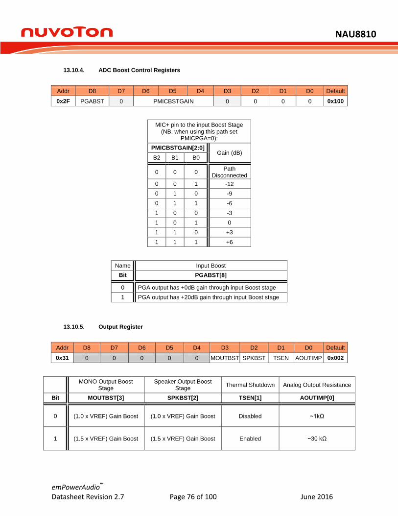
NAU8810
emPowerAudio™ Datasheet Revision 2.7 Page 76 of 100 June 2016
13.10.4. ADC Boost Control Registers
Addr D8 D7 D6 D5 D4 D3 D2 D1 D0 Default
0x2F PGABST 0 PMICBSTGAIN 0 0 0 0 0x100
MIC+ pin to the input Boost Stage (NB, when using this path set
PMICPGA=0):
PMICBSTGAIN[2:0] Gain (dB)
B2 B1 B0
0 0 0 Path
Disconnected
0 0 1 -12
0 1 0 -9
0 1 1 -6
1 0 0 -3
1 0 1 0
1 1 0 +3
1 1 1 +6
Name Input Boost
Bit PGABST[8]
0 PGA output has +0dB gain through input Boost stage
1 PGA output has +20dB gain through input Boost stage
13.10.5. Output Register
Addr D8 D7 D6 D5 D4 D3 D2 D1 D0 Default
0x31 0 0 0 0 0 MOUTBST SPKBST TSEN AOUTIMP 0x002
MONO Output Boost
Stage Speaker Output Boost
Stage Thermal Shutdown Analog Output Resistance
Bit MOUTBST[3] SPKBST[2] TSEN[1] AOUTIMP[0]
0 (1.0 x VREF) Gain Boost (1.0 x VREF) Gain Boost Disabled ~1kΩ
1 (1.5 x VREF) Gain Boost (1.5 x VREF) Gain Boost Enabled ~30 kΩ
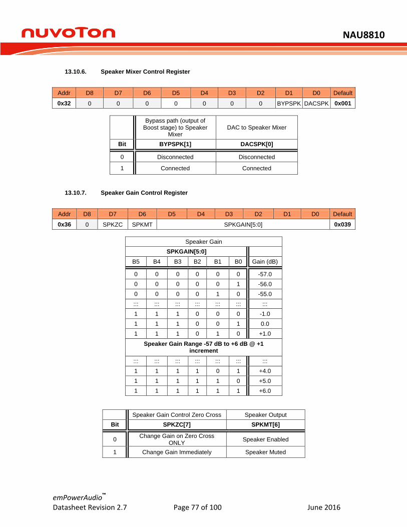
NAU8810
emPowerAudio™ Datasheet Revision 2.7 Page 77 of 100 June 2016
13.10.6. Speaker Mixer Control Register
Addr D8 D7 D6 D5 D4 D3 D2 D1 D0 Default
0x32 0 0 0 0 0 0 0 BYPSPK DACSPK 0x001
Bypass path (output of
Boost stage) to Speaker Mixer
DAC to Speaker Mixer
Bit BYPSPK[1] DACSPK[0]
0 Disconnected Disconnected
1 Connected Connected
13.10.7. Speaker Gain Control Register
Addr D8 D7 D6 D5 D4 D3 D2 D1 D0 Default
0x36 0 SPKZC SPKMT SPKGAIN[5:0] 0x039
Speaker Gain
SPKGAIN[5:0]
B5 B4 B3 B2 B1 B0 Gain (dB)
0 0 0 0 0 0 -57.0
0 0 0 0 0 1 -56.0
0 0 0 0 1 0 -55.0
::: ::: ::: ::: ::: ::: :::
1 1 1 0 0 0 -1.0
1 1 1 0 0 1 0.0
1 1 1 0 1 0 +1.0
Speaker Gain Range -57 dB to +6 dB @ +1 increment
::: ::: ::: ::: ::: ::: :::
1 1 1 1 0 1 +4.0
1 1 1 1 1 0 +5.0
1 1 1 1 1 1 +6.0
Speaker Gain Control Zero Cross Speaker Output
Bit SPKZC[7] SPKMT[6]
0 Change Gain on Zero Cross
ONLY Speaker Enabled
1 Change Gain Immediately Speaker Muted

NAU8810
emPowerAudio™ Datasheet Revision 2.7 Page 78 of 100 June 2016
13.10.8. MONO Mixer Control Register
Addr D8 D7 D6 D5 D4 D3 D2 D1 D0 Default
0x38 0 0 MOUTMXMT 0 0 0 0 BYPMOUT DACMOUT 0x001
MOUT Mute Bypass path (output of Boost Stage) to MONO
Mixer
DAC to MONO Mixer
Bit MOUTMXMT[6] BYPMOUT[1] DACMOUT[0]
0 Not Muted Disconnected Disconnected
1 Muted Connected Connected
During mute, the MONO output will output VREF that can be used as a DC reference for a headphone out.
13.10.9. Power Management 4
Addr D8 D7 D6 D5 D4 D3 D2 D1 D0 Default
0x3A LPIPBST LPADC LPSPKD LPDAC MICBIASM TRIMREG[3:2] IBADJ[1:0] 0x000
B1 B0
Trim Output Regulator (V) Adjust Master Bias of the Analog Portion
TRIMREG[3:2] IBADJ[1:0]
0 0 1.800 Default Current Consumption
0 1 1.610 25% Current Increase from Default
1 0 1.400 14% Current Decrease from Default
1 1 1.218 25% Current Decrease from Default
Trim regulator bits can be used only when VDDD <2.7V.
Low Power IP
Boost Low Power ADC
Low Power Speaker Driver Low Power DAC
Microphone bias Mode selection
Bit LPIPBST[8] LPADC[7] LPSPKD[6] LPDAC[5] MICBIASM[4]
0 Normal Function Normal Function Normal Function Normal Function Disable
1 Cut power in half Cut power in half Cut power in half Cut power in half Enable
Note cutting the power in half will directly affect the audio performances.

NAU8810
emPowerAudio™ Datasheet Revision 2.7 Page 79 of 100 June 2016
13.11. PCM TIME SLOT CONTROL & ADCOUT IMPEDANCE OPTION CONTROL
13.11.1. PCM1 TIMESLOT CONTROL REGISTER
Addr D8 D7 D6 D5 D4 D3 D2 D1 D0 Default
0x3B TSLOT[8:0] 0x000
Transmit and receive timeslot are expressed in number of BCLK cycles in a 10-bit word. The most significant bit
TSLOT[9] is located in register PCMTS2[0] address (0x3C). Timeslot, TSLOT[9:0], determines the start point for
the timeslot on the PCM interface for data in the transmit direction.
13.11.2. PCM2 TIMESLOT CONTROL REGISTER
Addr D8 D7 D6 D5 D4 D3 D2 D1 D0 Default
0x3C PCMTSEN TRI PCM8BIT PUDOEN PUDPE PUDPS LOUTR PCMB TSLOT[9] 0x000
Name PCM Transit
Enable Tri-state PCMT
LSB PCM Word Length
Left and Right Channel have
same data PCM Mode2
Bit PCMTSEN[8] TRI[7] PCM8BIT[6] LOUTR PCMB
0 PCM A Drive the full Clock of LSB
Use WLEN[6:5] to select Word Length
Disable Disable
1 PCM Time Slot Tri-State the 2
nd
half of LSB
Audio interface will be 8 Bit Word Length
Enable Enable
If TRI = 1 and PUDOEN = 0, the device will drive the LSB bit 1
st half of BCLK out of the ADCOUT pin (stop driving
after LSB BCLK Rising edge) but if TRI = 0 or PUDOEN = 1 this feature is disabled, full BCLK of LSB will be
driven the LSB value.
Figure 35: The Programmable ADCOUT Pin
PUDOE
ADCOUTiADCOUT
PUDPE
PUDPS

NAU8810
emPowerAudio™ Datasheet Revision 2.7 Page 80 of 100 June 2016
Internal ADC out data
Power Up and Down Output Enable
Power Up and Down Pull Enable
Power Up and Down Pull Select
OUTPUT
iADCOUT PUDOEN[5] PUDPE[4] PUDPS[3] PAD
0 1 x x 0
1 1 x x 1
x 0 0 x Hi-Z
x 0 1 0 Pull-Low
x 0 1 1 Pull-High
13.12. REGISTER ID
13.12.1. Device revision register
Addr D8 D7 D6 D5 D4 D3 D2 D1 D0 Default
0x3E 0 1 1 1 0 1 1 1 0 0x0EE
Device revision ID
13.12.2. 2-WIRE ID Register
Addr D8 D7 D6 D5 D4 D3 D2 D1 D0 Default
0x3F 0 0 0 0 1 1 0 1 0 0x01A
First 7 bits (D0 – D6) of the 2-Wire device ID excluding the LSB /write bit.
13.12.3. Additional ID
Addr D8 D7 D6 D5 D4 D3 D2 D1 D0 Default
0x40 0 1 1 0 0 1 0 1 0 0x0CA
ONLY
13.13. Reserved
Addr D8 D7 D6 D5 D4 D3 D2 D1 D0 Default
0x41 1 0 0 1 0 0 1 0 0 0x124

NAU8810
emPowerAudio™ Datasheet Revision 2.7 Page 81 of 100 June 2016
13.14. OUTPUT Driver Control Register
Addr D8 D7 D6 D5 D4 D3 D2 D1 D0 Default
0x45 0 SPKMOUT MOUTMT 0 HVOPU 0 HVOP 0x001
Bit Location Bit Description Bit Name
Bit Value
0 1
0 Override to automatic 3V/5V bias selection
HVOP
set internal output biasing to be optimal for 3.6Vdc or lower operation Note: For this to be effective HVOPU[2] address 0x45 must set
set internal output biasing to be optimal for higher than 3.6Vdc operation Note: For this to be effective HVOPU[2] address 0x45 must set
2 Update bit for HV override feature
HVOPU High Voltage override Disable
This bit must set in conjunction with HVOP[0] address 0x45 for the automatic override to be effective
4 Headphone output mute MOUTMT Disable Enable
5 Speaker signals go to MOUT
SPKMOUT Disable Enable
During mute, the MONO output will output VREF that can be used as a DC reference for a headphone out.

NAU8810
emPowerAudio™ Datasheet Revision 2.7 Page 82 of 100 June 2016
13.15. AUTOMATIC LEVEL CONTROL ENHANCED REGISTER
13.15.1. ALC1 Enhanced Register
Addr D8 D7 D6 D5 D4 D3 D2 D1 D0 Default
0x46 ALCTBLSEL ALCPKSEL ALCNGSEL ALCGAIN ( ONLY) 0x001
Bit Location
Bit Description Bit Name Bit Value
0 1
6 Selects one of two tables used to set the target level for the ALC
ALCNGSEL default recommended target level table spanning -1.5dB through -22.5dB FS
optional ALC target level table spanning -6.0dB through -28.5dB FS
7 Choose peak or peak-to-peak value for ALC threshold logic
ALCPKSEL use rectified peak detector output value
use peak-to-peak detector output value
8 Choose peak or peak-to-peak value for Noise Gate threshold logic
ALCTBLSEL use rectified peak detector output value
use peak-to-peak detector output value
13.15.2. ALC Enhanced 2 Register
Addr D8 D7 D6 D5 D4 D3 D2 D1 D0 Default
0x47 PKLIMEN 0 0x000
Bit Location
Bit Description Bit Name Bit Value
0 1
8 Enable control for ALC fast peak limiter function
PKLIMEN Enable Disable
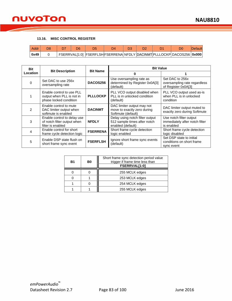
NAU8810
emPowerAudio™ Datasheet Revision 2.7 Page 83 of 100 June 2016
13.16. MISC CONTROL REGISTER
Addr D8 D7 D6 D5 D4 D3 D2 D1 D0 Default
0x49 0 FSERRVAL[1:0] FSERFLSH FSERRENA NFDLY DACINMT PLLLOCKP DACOS256 0x000
Bit Location
Bit Description Bit Name Bit Value
0 1
0 Set DAC to use 256x oversampling rate
DACOS256 Use oversampling rate as determined by Register 0x0A[3] (default)
Set DAC to 256x oversampling rate regardless of Register 0x0A[3]
1 Enable control to use PLL output when PLL is not in phase locked condition
PLLLOCKP PLL VCO output disabled when PLL is in unlocked condition (default)
PLL VCO output used as-is when PLL is in unlocked condition
2 Enable control to mute DAC limiter output when softmute is enabled
DACINMT DAC limiter output may not move to exactly zero during Softmute (default)
DAC limiter output muted to exactly zero during Softmute
3 Enable control to delay use of notch filter output when filter is enabled
NFDLY Delay using notch filter output 512 sample times after notch enabled (default)
Use notch filter output immediately after notch filter is enabled
4 Enable control for short frame cycle detection logic
FSERRENA Short frame cycle detection logic enabled
Short frame cycle detection logic disabled
5 Enable DSP state flush on short frame sync event
FSERFLSH Ignore short frame sync events (default)
Set DSP state to initial conditions on short frame sync event
B1 B0 Short frame sync detection period value
trigger if frame time less than
FSERRVAL[1:0]
0 0 255 MCLK edges
0 1 253 MCLK edges
1 0 254 MCLK edges
1 1 255 MCLK edges

NAU8810
emPowerAudio™ Datasheet Revision 2.7 Page 84 of 100 June 2016
13.17. Output Tie-Off REGISTER
Addr D8 D7 D6 D5 D4 D3 D2 D1 D0 Default
0x4B 0 LPSPKA MANVREFH MANVREFM MANVREFL 0x000
Bit Location
Bit Description Bit Name Bit Value
0 1
0 Direct manual control for switch for VREF 6k-ohm resistor to ground
MANVREFL switch to ground controlled by Register 0x01 setting
switch to ground in the closed position
1 Direct manual control for switch for VREF 160k-ohm resistor to ground
MANVREFM switch to ground controlled by Register 0x01 setting
switch to ground in the closed position
2 Direct manual control of switch for VREF 600k-ohm resistor to ground
MANVREFH switch to ground controlled by Register 0x01 setting
switch to ground in the closed position
7 Amplifier Stage LPSPKA Two-stage amplifier for
speaker driver Three-stage amplifier for
speaker driver
13.18. AGC PEAK-TO-PEAK OUT REGISTER
Addr D8 D7 D6 D5 D4 D3 D2 D1 D0 Default
0x4C P2PDET 0x000
Bit Location
Bit Description Bit Name
0 – 8
ONLY Register Outputs the instantaneous value contained in the peak-to-peak amplitude register used by the ALC for signal level dependent logic. Value is highest of left or right input when both inputs are under ALC control.
P2PDET
13.19. AGC PEAK OUT REGISTER
Addr D8 D7 D6 D5 D4 D3 D2 D1 D0 Default
0x4D PDET 0x000
Bit Location
Bit Description Bit Name
0 – 8
ONLY Register Outputs the instantaneous value contained in the peak detector amplitude register used by the ALC for signal level dependent logic. Value is highest of left or right input when both inputs are under ALC control.
PDET

NAU8810
emPowerAudio™ Datasheet Revision 2.7 Page 85 of 100 June 2016
13.20. AUTOMUTE CONTROL AND STATUS REGISTER
Addr D8 D7 D6 D5 D4 D3 D2 D1 D0 Default
0x4E 0 0 AMTCTRL HVDET NSGATE AMUTE DMUTE 0 FTDEC 0x000
Bit Location
Bit Description Bit Name Bit Value
0 1
0 Peak limiter indicator FASTDEC Below 87.5% of full scale Above 87.5% of full scale
2 ONLY BIT Digital Mute function of the DAC
DMUTE Digital gain greater than zero Digital gain is zero either by .- Direct setting .- Softmute function
3 ONLY BIT Analog Mute function applied to DAC
AMUTE Automute Disabled Automute Enabled
4 ONLY BIT Logic controlling the Noise Gate
NSGATE Signal is greater than the noise gate threshold and ALC gain can change
Signal is less than the noise gate threshold and ALC gain is held constant
5 ONLY BIT High voltage detection circuit monitoring VDDSPK voltage
HVDET VDDSPK logic switch voltage threshold measured as 4.0Vdc or Less
VDDSPK logic switch voltage threshold measured as 4.0Vdc or Greater
6 Select observation point used by DAC output Automute feature
AMTCTRL Automute operates on data at the input to the DAC digital attenuator (default)
Automute operates on data at the DACIN input pin
13.21. Output Tie-off Direct Manual Control REGISTER
Addr D8 D7 D6 D5 D4 D3 D2 D1 D0 Default
0x4F MANOUTEN SBUFH SBUFL SNSPK SPSPK SMOUT 0 0 0 0x000
Bit Location
Bit Description Bit Name Bit Value
0 1
3 If MANUOUTEN = 1, use this bit to control Auxout1 output tie-off resistor switch
SMOUT Tie-off resistor switch for MOUT output is forced open
Tie-off resistor switch for MOUT output is forced closed
4 If MANUOUTEN = 1, use this bit to control left speaker output Tie-off resistor switch
SPSPK Tie-off resistor switch for SPKOUTP speaker output is forced open
Tie-off resistor switch for SPKOUTP speaker output is forced closed
5 If MANUOUTEN = 1, use this bit to control left speaker output Tie-off resistor switch
SNSPK Tie-off resistor switch for SPKOUTN speaker output is forced open
Tie-off resistor switch for SPKOUTN speaker output is forced closed
6
If MANUOUTEN = 1, use this bit to control bypass switch around 1.0x non-boosted output Tie-off buffer amplifier
SBUFL Normal automatic operation of bypass switch
Bypass switch in closed position when output buffer amplifier is disabled
7
If MANUOUTEN = 1, use this bit to control bypass switch around 1.5x boosted output Tie-off buffer amplifier
SBUFH Normal automatic operation of bypass switch
Bypass switch in closed position when output buffer amplifier is disabled
8 Enable direct control over output Tie-off resistor switching
MANOUTEN Ignore Register 0x4F bits to control input Tie-off resistor/buffer switching
Use Register 0x4F bits to override automatic Tie-off resistor/buffer switching
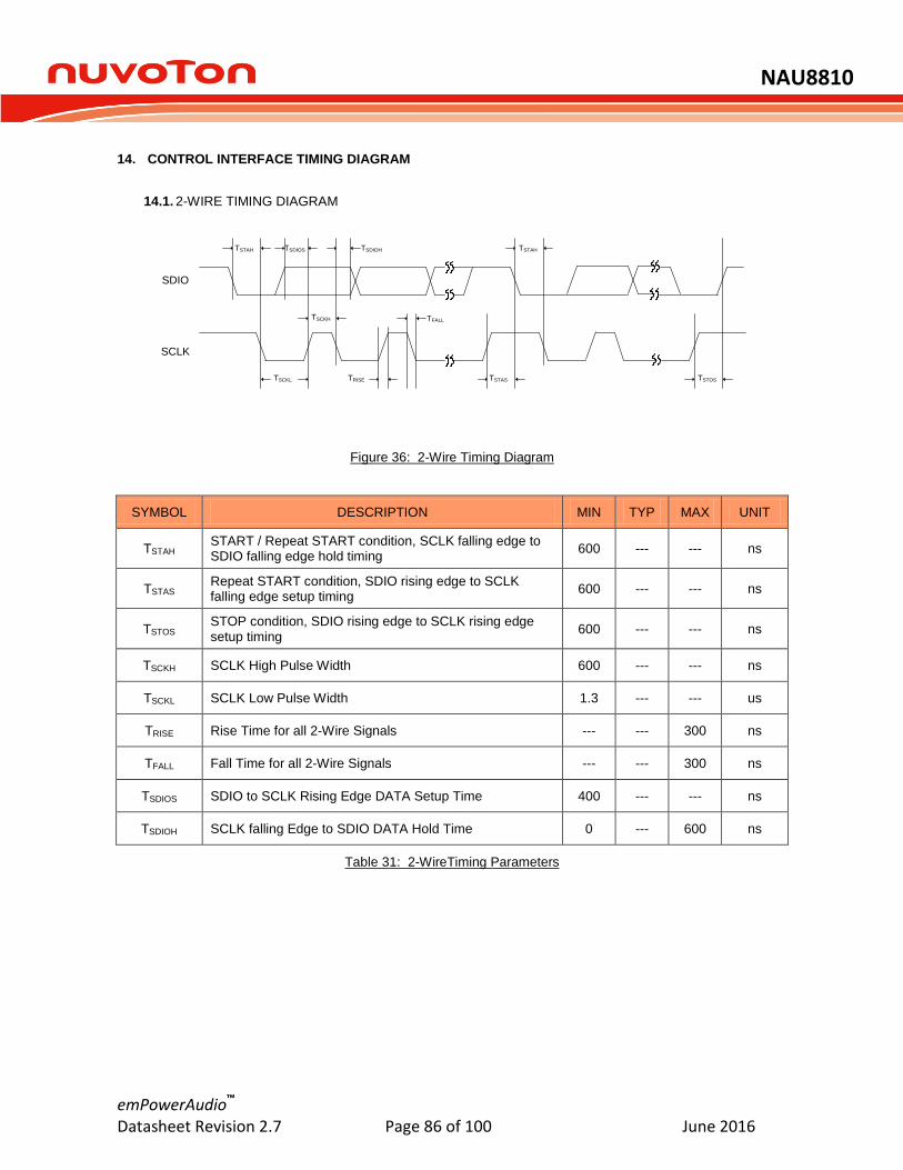
NAU8810
emPowerAudio™ Datasheet Revision 2.7 Page 86 of 100 June 2016
14. CONTROL INTERFACE TIMING DIAGRAM
14.1. 2-WIRE TIMING DIAGRAM
TSTAH TSTAH
TSTOSTSTAS
TSDIOS TSDIOH
TSCKL
TSCKH
TRISE
TFALL
SCLK
SDIO
Figure 36: 2-Wire Timing Diagram
SYMBOL DESCRIPTION MIN TYP MAX UNIT
TSTAH START / Repeat START condition, SCLK falling edge to SDIO falling edge hold timing
600 --- --- ns
TSTAS Repeat START condition, SDIO rising edge to SCLK falling edge setup timing
600 --- --- ns
TSTOS STOP condition, SDIO rising edge to SCLK rising edge setup timing
600 --- --- ns
TSCKH SCLK High Pulse Width 600 --- --- ns
TSCKL SCLK Low Pulse Width 1.3 --- --- us
TRISE Rise Time for all 2-Wire Signals --- --- 300 ns
TFALL Fall Time for all 2-Wire Signals --- --- 300 ns
TSDIOS SDIO to SCLK Rising Edge DATA Setup Time 400 --- --- ns
TSDIOH SCLK falling Edge to SDIO DATA Hold Time 0 --- 600 ns
Table 31: 2-WireTiming Parameters

NAU8810
emPowerAudio™ Datasheet Revision 2.7 Page 87 of 100 June 2016
15. AUDIO INTERFACE TIMING DIAGRAM
15.1. AUDIO INTERFACE IN SLAVE MODE
TFSH
TFSS
TFSH
TFSS
TDIS
TDIH
TDOD
TBCK
TBCKH
TBCKL
TRISETFALL
BCLK
(Slave)
FS
(Slave)
DACIN
ADCOUT
Figure 37: Audio Interface Slave Mode Timing Diagram
15.2. AUDIO INTERFACE IN MASTER MODE
TFSD TFSD
TDIS
TDIH
TDOD
BCLK
(Master)
FS
(Master)
DACIN
ADCOUT
Figure 38: Audio Interface in Master Mode Timing Diagram

NAU8810
emPowerAudio™ Datasheet Revision 2.7 Page 88 of 100 June 2016
15.3. PCM AUDIO INTERFACE IN SLAVE MODE (PCM Audo Data)
Figure 39: PCM Audio Interface Slave Mode Timing Diagram
15.4. PCM AUDIO INTERFACE IN MASTER MODE (PCM Audo Data)
Figure 40: PCM Audio Interface Slave Mode Timing Diagram
TFSH
TFSS
TFSH
TFSS
TDIS
TDIH
TDOD
TBCK
TBCKH
TBCKL
TRISETFALL
BCLK
(Slave)
FS
(Slave)
DACIN
ADCOUT MSB
MSB
TFSD TFSD
TDIS
TDIH
TDOD
BCLK
(Master)
FS
(Master)
DACIN
ADCOUT
MSB
MSB
TFSD

NAU8810
emPowerAudio™ Datasheet Revision 2.7 Page 89 of 100 June 2016
15.5. PCM AUDIO INTERFACE IN SLAVE MODE (PCM Time Slot Mode )
TFSH
TFSS
TFSH
TFSS
TDIS
TDIH
TDOD
TBCK
TBCKH
TBCKL
TRISETFALL
BCLK
(Slave)
FS
(Slave)
DACIN
ADCOUT
TDOD1
MSB
MSB
Figure 41: PCM Audio Interface Slave Mode (PCM Time Slot Mode )Timing Diagram
15.6. PCM AUDIO INTERFACE IN MASTER MODE (PCM Time Slot Mode )
TFSD TFSD
TDIS
TDIH
TDOD
BCLK
(Master)
FS
(Master)
DACIN
ADCOUT
MSB
MSB
Figure 42: PCM Audio Interface Master Mode (PCM Time Slot Mode )Timing Diagram

NAU8810
emPowerAudio™ Datasheet Revision 2.7 Page 90 of 100 June 2016
SYMBOL DESCRIPTION MIN TYP MAX UNIT
TBCK BSCK Cycle Time (Slave Mode) 50 --- --- ns
TBCKH BSCK High Pulse Width (Slave Mode) 20 --- --- ns
TBCKL BSCK Low Pulse Width (Slave Mode) 20 --- --- ns
TFSS fs to SCK Rising Edge Setup Time (Slave Mode) 20 --- --- ns
TFSH SCK Rising Edge to fs Hold Time (Slave Mode) 20 --- --- ns
TFSD fs to SCK falling to fs transition (Master Mode) --- --- 10 ns
TRISE Rise Time for All Audio Interface Signals --- --- 0.135TBCK ns
TFALL Fall Time for All Audio Interface Signals --- --- 0.135TBCK ns
TDIS ADCIN to SCK Rising Edge Setup Time 15 --- --- ns
TDIH SCK Rising Edge to ADCIN Hold Time 15 --- --- ns
TDOD Delay Time from SCLK falling Edge to DACOUT --- --- 10 ns
Table 32: Audio Interface Timing Parameters
15.7. System Clock (MCLK) Timing Diagram
Figure 43: MCLK Timing Diagram
PARAMETER SYMBOL TEST CONDITIONS MIN TYP MAX UNIT
MCLK Duty Cycle TMCLKDC 60:40 40:60
MCLK High Pulse Width TMCLKH 20 --- --- ns
MCLK Low Pulse Width TMCLKL 20 --- --- ns
Table 33: MCLK Timing Parameter
TMCLKL
MCLK
TMCLKH

NAU8810
emPowerAudio™ Datasheet Revision 2.7 Page 91 of 100 June 2016
15.8. µ-LAW ENCODE DECODE CHARACTERISTICS
Normalized Encode Decision Levels
Digital Code Normalized
Decode Levels
D7 D6 D5 D4 D3 D2 D1 D0
Sign Chord Chord Chord Step Step Step Step
8159
1 0 0 0 0 0 0 0 8031
7903
: : : : : : : : : :
4319
1 0 0 0 1 1 1 1 4191
4063
: : : : : : : : : :
2143
1 0 0 1 1 1 1 1 2079
2015
: : : : : : : : : :
1055
1 0 1 0 1 1 1 1 1023
991
: : : : : : : : : :
511
1 0 1 1 1 1 1 1 495
479
: : : : : : : : : :
239
1 1 0 0 1 1 1 1 231
223
: : : : : : : : : :
103
1 1 0 1 1 1 1 1 99
95
: : : : : : : : : :
35
1 1 1 0 1 1 1 1 33
31
: : : : : : : : : :
3
1 1 1 1 1 1 1 0 2
1 : : : : : : : : :
1 1 1 1 1 1 1 1 0
0
Notes: Sign bit = 0 for negative values, sign bit = 1 for positive values

NAU8810
emPowerAudio™ Datasheet Revision 2.7 Page 92 of 100 June 2016
15.9. A-LAW ENCODE DECODE CHARACTERISTICS
Normalized Encode Decision Levels
Digital Code Normalized
Decode Levels
D7 D6 D5 D4 D3 D2 D1 D0
Sign Chord Chord Chord Step Step Step Step
4096
1 0 1 0 1 0 1 0 4032
3968
: : : : : : : : : :
2176
1 0 1 0 0 1 0 1 2112
2048
: : : : : : : : : :
1088
1 0 1 1 0 1 0 1 1056
1024
: : : : : : : : : :
544
1 0 0 0 0 1 0 1 528
512
: : : : : : : : : :
272
1 0 0 1 0 1 0 1 264
256
: : : : : : : : : :
136
1 1 1 0 0 1 0 1 132
128
: : : : : : : : : :
68
1 1 1 0 0 1 0 1 66
64
: : : : : : : : : :
2
1 1 0 1 0 1 0 1 1
0
Notes: 1. Sign bit = 0 for negative values, sign bit = 1 for positive values 2. Digital code includes inversion of all even number bits

NAU8810
emPowerAudio™ Datasheet Revision 2.7 Page 93 of 100 June 2016
15.10. µ-LAW / A-LAW CODES FOR ZERO AND FULL SCALE
Level
µ-Law A-Law
Sign bit (D7)
Chord bits (D6,D5,D4)
Step bits (D3,D2,D1,D0)
Sign bit (D7)
Chord bits (D6,D5,D4)
Step bits (D3,D2,D1,D0)
+ Full Scale 1 000 0000 1 010 1010
+ Zero 1 111 1111 1 101 0101
- Zero 0 111 1111 0 101 0101
- Full Scale 0 000 0000 0 010 1010
15.11. µ-LAW / A-LAW OUTPUT CODES (DIGITAL MW)
Sample
µ-Law A-Law
Sign bit (D7)
Chord bits (D6,D5,D4)
Step bits (D3,D2,D1,D0)
Sign bit (D7)
Chord bits (D6,D5,D4)
Step bits (D3,D2,D1,D0)
1 0 001 1110 0 011 0100
2 0 000 1011 0 010 0001
3 0 000 1011 0 010 0001
4 0 001 1110 0 011 0100
5 1 001 1110 1 011 0100
6 1 000 1011 1 010 0001
7 1 000 1011 1 010 0001
8 1 001 1110 1 011 0100

NAU8810
emPowerAudio™ Datasheet Revision 2.7 Page 94 of 100 June 2016
16. DIGITAL FILTER CHARACTERISTICS
PARAMETER TEST
CONDITIONS MIN TYP MAX UNIT
ADC Filter
Passband
+/- 0.025dB 0 0.454*fs
-6dB 0.5*fs
Passband Ripple +/-0.025 dB
Stopband 0.546*fs
Stopband Attenuation
f > 0.546*fs -60 dB
Group Delay 21/fs
ADC High Pass Filter
High Pass Filter Corner Frequency
-3dB 3.7
Hz -0.5dB 10.4
-0.1dB 21.6
DAC Filter
Passband
+/- 0.035dB 0 0.454*fs
-6dB 0.5*fs
Passband Ripple +/-0.035 dB
Stopband 0.546*fs
Stopband Attenuation
f > 0.546*fs -55 dB
Group Delay 29/fs
Table 57 Digital Filter Characteristics TERMINOLOGY
1. Stop Band Attenuation (dB) – the degree to which the frequency spectrum is attenuated (outside audio band) 2. Pass-band Ripple – any variation of the frequency response in the pass-band region 3. Note that this delay applies only to the filters and does not include

NAU8810
emPowerAudio™ Datasheet Revision 2.7 Page 95 of 100 June 2016
Figure 44: DAC Filter Frequency Response
Figure 45: ADC Filter Frequency Response
Figure 46: DAC Filter Ripple
Figure 47: ADC Filter Ripple

NAU8810
emPowerAudio™ Datasheet Revision 2.7 Page 96 of 100 June 2016
17. TYPICAL APPLICATION
Figure 48: Application Diagram For 20-Pin QFN Note 1: All non-polar capacitors are assumed to be low ESR type parts, such as with MLC construction or similar.
If capacitors are not low ESR, additional 0.1uF and/or 0.01uF capacitors may be necessary in parallel with the bulk 4.7uF capacitors on the supply rails.
Note 2: Load resistors to ground on outputs may be helpful in some applications to insure a DC path for the
output capacitors to charge/discharge to the desired levels. If the output load is always present and the output load provides a suitable DC path to ground, then the additional load resistors may not be necessary. If needed, such load resistors are typically a high value, but a value dependent upon the application requirements.
Note 3: To minimize pops and clicks, large polarized output capacitors should be a low leakage type. Note 4: Depending on the microphone device and PGA gain settings, common mode rejection can be improved
by choosing the resistors on each node of the microphone such that the impedance presented to any noise on either microphone wire is equal.

NAU8810
emPowerAudio™ Datasheet Revision 2.7 Page 97 of 100 June 2016
18. PACKAGE SPECIFICATION

NAU8810
emPowerAudio™ Datasheet Revision 2.7 Page 98 of 100 June 2016
19. ORDERING INFORMATION
Nuvoton Part Number Description
NAU88U10Y G
Package Type:
Y = 20-Pin QFN Package
Package Material:
G = Pb-free Package
Feature:
U = AEC-Q100

NAU8810
emPowerAudio™ Datasheet Revision 2.7 Page 99 of 100 June 2016
20. VERSION HISTORY
VERSION DATE PAGE DESCRIPTION
1.0 September
2010 Preliminary Revision
1.1 October 2010 95 Updated Applications Diagram
1.2 January 2011
57
73
89
Corrected Register 0x38 Register name
Improved description of Mic Bias set up
Added TMCLKH and TMCLKL parameters to table
1.3 October 2013 85
14
Corrected 2 wire timing diagram
Corrected Digital I/O voltage levels from DCVDD to DBVDD
1.4 Nov. 7, 2013
11
11
95
Modify operating condition from VDDA≥VDDC to VDDA≥VDDB.
Modify the VDDSPK operating condition
Modify Figure 48 (Application Diagram For 20-Pin QFN)
1.5 Nov. 7, 2013 95 Modify Figure 48, replace the VSSA with the symbol of analog
ground
1.6 Jan. 15, 2014
12 – 14
43
44
An additional remark of VDDSPK boost mode
Modify Figure 23 (Byte Write Sequence)
Modify Figure 24 (2-Wire Read Sequence)
1.7 Mar. 27, 2014
11-14, 51,
53, 54
13
89
Modified VDDB and VDDC to VDDD
Corrected headphone full scale output
Corrected rising/falling time specification of I2S
1.8 July 2, 2014 3
23
Pin 11 and 12 functionalities are updated.
Added more descriptions to figure 8.
1.9 Nov,2014 85 Corrected Tsdios setup time
2.0 Jan,2015 1 and 98 Updated AEC-Q100 description note and ordering information
2.1 May 2015 98 Correct a typing error. Modify “contract “ to “contact”
2.2 July 2015 23,65 Change 3.7KHz to 3.7Hz
2.3 Sep,2015 81 Added Reg0x45[5] for SPKMOUT
2.4 Oct, 2015 37 Added 12.6.3 session for differential output configuration
2.5 Feb, 2016 1 Updated AEC-Q100 description
2.6 March 2016 35 Add Important Notice
2.7 June, 2016 43
82
Revise f1 equation from * to /
Add Slicon Revision ID

NAU8810
emPowerAudio™ Datasheet Revision 2.7 Page 100 of 100 June 2016
Important Notice
Nuvoton Products are neither intended nor warranted for usage in systems or equipment, any malfunction or failure of which may cause loss of human life, bodily injury or severe property damage. Such applications are deemed, “Insecure Usage”.
Insecure usage includes, but is not limited to: equipment for surgical implementation, atomic energy control instruments, airplane or spaceship instruments, the control or operation of dynamic, brake or safety systems designed for vehicular use, traffic signal instruments, all types of safety devices, and other applications intended to support or sustain life.
All Insecure Usage shall be made at customer’s risk, and in the event that third parties lay claims to Nuvoton as a result of customer’s Insecure Usage, customer shall indemnify the damages and liabilities thus incurred by Nuvoton.