Embed Size (px)
Citation preview

/
.I- .,. * ' . "
SEMIANNUAL REPORT NASA RESEARCH GRANT NGR-22-011-007
RELIABLE SOLID-STATE CIRCUITS
bY
R. E. Bach, Jr. A. W. Carlson
C. A. Furciniti
R. E. Scott
? ., , .
Electronics Research Laboratory
Northeastern University
Boston, Mass.
July I, 1965
https://ntrs.nasa.gov/search.jsp?R=19660002510 2018-06-10T17:54:07+00:00Z

SEMIANNUAL REPORT
NASA RESEARCH GRANT NGR-22-011-007
RELIABLE SOLID-STATE CIRCUITS
by
R. E . B a c h , Jr .
A . W. C a r l s o n
C. A . P u r c i n i t i
R . E. S c o t t
E l e c t r o n i c s R e s e a r c h L a b o r a t o r y
Northeastern U n i v e r s i t y
B o s t o n , Mass.
J u l y 1, 1965

The research reported here covers the period from December 1, 1 9 6 4 - May 31, 1 9 6 5 ,
and was sponsored by the National Aeronautics and Space Administration under Research
Grant NGR-22-011-007. This report is published for information purposes only and does
not represent recommendations or conclusions of the sponsoring agency. Reproduction
in whole or part is permitted for any purpose of the United States Government.

.
RESEARCH STAFF
Ralph E. Bach, Jr., Co-Principal Investigator
Associate Professor of Electrical Engineering
A. William Carlson, Co-Principal Investigator Senior Research Associate
Charles A. Furciniti
Res ear ch Associate
Ronald E. Scott Dean of the College of Engineering

ACKNOWLEDGMENT
The authors would like to extend their gratitude to Professor William F. King
of the Electrical Engineering Department for his cooperation in providing equipment
for use in the Grant Laboratory. Special thanks are given to Mr. William Fabrizio
for his able service as lab technician and to Miss Martha Wright and Mr. Fabrizio for
their enthusiastic and efficient processing of the manuscript.

TABLE OF CONTENTS
Page
RESEARCH STAFF
ACKNOWLEDGMENT
TABLE OF CONTENTS
LIST OF FIGURES AND TABLES
I. INTRODUCTION
1.1 System requirements
1.2 Circuit development
1.3 Microminiaturization
11. SWITCHING AMPLIFIER ANALYSIS
2.1 Pulse-width modulation (PWM)
2.2 Analysis of PWM systems
2.2.1 Simple RC feedback
2.2.2 Modified RC feedback
2.2.3 Synchronous operation
2.3 Comparison of PWM systems
111. SWITCHING AMPLIFIER DESIGN
3.1
3.1.1
3.1.2
3.1.3
3.1.4
3.2
3.2.1
3.2.2
3.2.3
3.3
3.3.1
3.3.2
3.3.3
Power stage considerations
Problems of driving an inductive load
Choice of switching frequency
Amplifier bandwidth
Overload and step response
Self-oscillating switching amplifiers: Hysteresis type
Stability considerat ions
Gain and distortion
Efficiency
Self-oscillating switching amplifiers: Delay type
Stability considerat ions
Gain and distortion
Thresholding
iii
iv
V
vii
3
3
5 7 8
9
10
13
14
14
16 16
18
18 20
20
21
21
23
23
25
- v -

3.4 Open-loop switching amplifier
3.4.1 Selection of switching waveshape
3.4.2 Differential amplifier
3.4.3 Gain and distortion
3.5 Microcircuit power considerations
3.5.1 Microcircuit practicality
IV. RELIABILITY CONSIDERATIONS
4.1 Conventional reliability theory
4.2 Reliability based on performance degradation
4.3 Redundancy: Majority voting
4.4 Redundancy: Analog
V. CONCLUSIONS AND RESEARCH PLANS
VI. REFERENCES
APPENDIX A
COMPARISON OF TWO-STATE MODULATOR AND MULTIVIBRATOR OPERATION
A.l System operation
A.2 Equivalent multivibrator
APPENDIX B OSCILLATOR AMPLITUDE REGULATION USING THE UNIJUNCTION TRANSISTOR
B.l Amplitude regulation
B.2 The unijunction transistor
B.3 Oscillator circuits
Page
25
25
27
28
28
29
34
34
35
35
36
42
44
45
45
46
51
51
51
54
- vi -
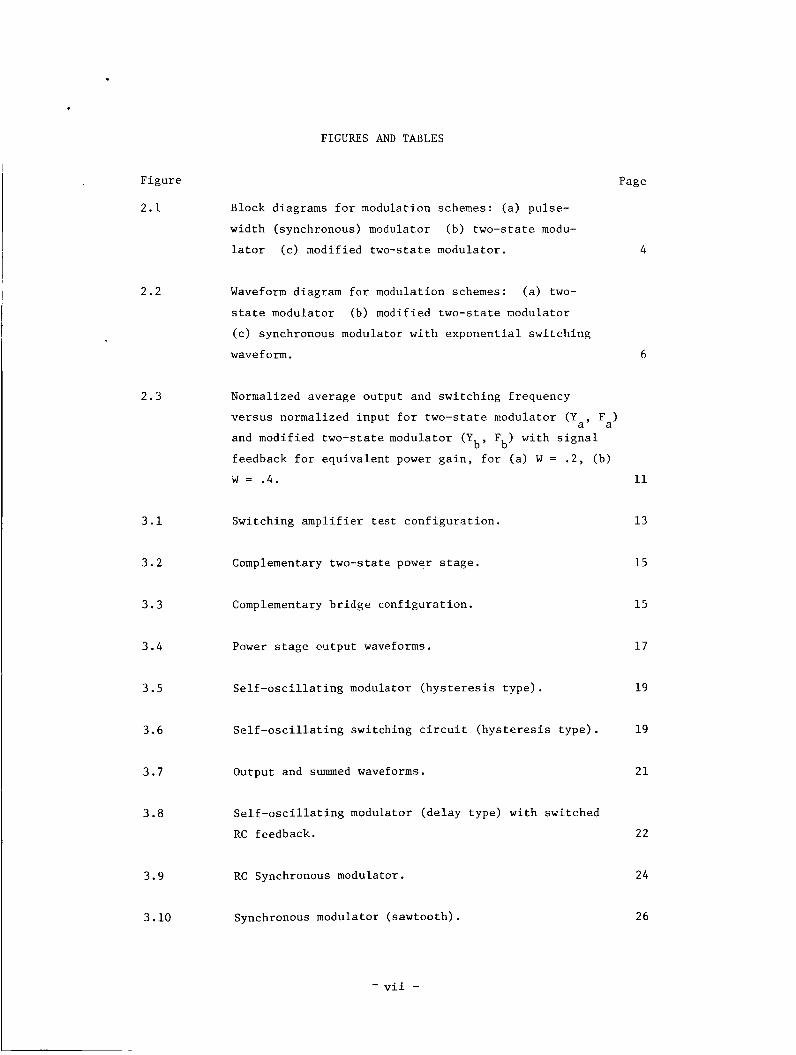
FIGURES AND TABLES
Page Figure
2 . 1
2 . 2
2 . 3
3.1
3 .2
3 . 3
3 . 4
3 .5
3.6
3.7
3.8
3.9
3.10
Block diagrams for modulation schemes: (a) pulse-
width (synchronous) modulator (b) two-state modu-
lator (c) modified two-state modulator. 4
Waveform diagram for modulation schemes: ( a ) two-
state modulator (b) modified two-state modulator
(c) synchronous modulator with exponential switching
waveform. 6
Normalized average output and switching frequency
versus normalized input for two-state modulator (Y and modified two-state modulator (Y F ) with signal
feedback for equivalent power gain, for (a) W = . 2 , (b)
w = . 4 . 11
Fa) a’
b’ b
Switching amplifier test configuration. 13
Complementary two-state power stage. 15
Complementary bridge configuration. 15
Power stage output waveforms. 17
Self-oscillating modulator (hysteresis type). 19
Self-oscillating switching circuit (hysteresis type). 19
Output and summed waveforms.
Self-oscillating modulator (delay type) with switched
RC feedback.
RC Synchronous modulator.
Synchronous modulator (sawtooth).
2 1
22
24
26
- vii -

Figure
3.11
3.12
3.13
4.1
4.2
4.3
4.4
4.5
A.l
A. 2
B.l
B.2
B.3
B.4
Sawtooth and PWM output signals.
Page
27
Modulation limits of PWM output. 29
Possible monolithic power stage (bridge). 30
Majority voting system. 36
TRISAFE scheme for reliable amplifier operation. 37
Feedforward scheme for reliable amplifier operation. 38
Operation of feedforward configuration when the
amplifiers saturate. 40
Three-amplifier analog computer representation of
feedforward scheme. 40
Block diagram of two-state modulator. 45
( a ) Astable multivibrator with modulation. (b) Multi-
vibrator V-I characteristic ( s = 0). (c) Multivibrator
V'-I' characteristic (with modulation). 47
Vb2-Ib2 unijunction characteristic. 52
Incremental resistance versus voltage (V ) for a
2N489 unijunction transistor. 53 b2
(a) Typical feedback amplifier used in (b) Wien-
bridge oscillator. 54
Wien-bridge oscillator circuits showing two ways of
using unijunction transistors for amplitude control. 55

Table
2.1
2.2
3.1
3.2
Page
Comparison of period variation with signal level for
pulse-width modulation systems. 10
Comparison of zero-signal gain and nonlinearity at
full modulation for pulse-width modulation systems 12
Area of integrated components 32
Comparison of different types of switching amplifiers 33
- ix -

I. Introduction
The central theme of the research reported here is the application of advanced
circuit concepts for realization of highly reliable and efficient electronic subsystems
that meet NASA mission requirements. Such subsystems must be designed for ultimate
microminiaturization. To achieve the stated objectives, the research effort during
the first six months of the grant period has been directed as outlined in the following
discussion.
1.1 System requirements.
Electronic system specifications for NASA spacecraft have been investigated by
gathering and examining information concerning mission objectives, system block diagrams
and specific circuits for several satellite programs. Of specific help in the continu-
ation of this work is the ready availability of technical documents, which has been made
possible by the Scientific and Technical Information Division of NASA. This agency
has placed the Northeastern University Library on the initial automatic distribution
list for STAR, unclassified NASA formal series reports, and NASA microfiche.
General requirements for electronic systems in space are:
(1) Low power, high efficiency,
(2) Small size, weight,
( 3 ) High reliability.
Requirement (l), above, was significant in the decision to investigate the use of
switching techniques for linear power amplification. Requirement ( 2 ) leads naturally
to the consideration of integrated circuit concepts for system design. Requirement
( 3 ) , reliability, is of prime importance in any space system realization, and figures
significantly in the work reported here and in the future research effort to be made
under this grant. Some specific ideas in this regard are discussed in Chapter IV.
1.2 Circuit Development.
Laboratory development of solid-state circuitry concurrent with the above pro-
gram has been emphasized. A basic effort has involved the use of switching devices to achieve linear power amplification. This technique has the advantage of high effi-
ciency, low distortion and independence of nonlinearities in the active region of the
switching device. A full discussion of this work is found in Chapters I1 and 111. Some experimentation has also been done on a novel scheme for amplitude regula-
tion of an oscillator. The use of a small lamp for oscillator regulation has been
- 1 -

standard practice for some time, but it has been found that the desired regulation
can instead be accomplished by the use of a unijunction transistor in a feedback net-
work which should be easily microminiaturized. This circuit application is covered
in Appendix B.
1.3 Microminiaturization
The development of integrated circuit techniques has made possible marked im-
provement in system reliability. Not only have interconnection problems diminished,
but it is now apparent that radiation tolerance has improved due to accompanying mate-
rials research. Furthermore, it is now feasible to shield complete circuits with only
a small increase in weight. Because of the small size of integrated circuits, the
structure necessary for support is smaller than that for conventional circuitry and
the connector size and number of connections are reduced. All of this leads to a weight
saving in the spacecraft with an attendant increase in electronic capability or reduc-
tion in vehicle power requirements.
An extensive investigation of the advantages and disadvantages of circuit de-
sign for microminiaturization has been carried out. Compatibility with this rapidly
advancing technology is a major factor in the design of electronic systems for space-
craft. Some important aspects of microcircuit design pertaining to the electronic
systems investigated during this period are discussed in Chapter 111.

11. Swi tch ing Ampl i f ie r Analys is
2 . 1 Pulse-width modulat ion (PWM) . I n t h i s c h a p t e r two schemes f o r achiev ing h igh ly r e l i a b l e l i n e a r power a m p l i f i -
c a t i o n are cons idered and e v a l u a t e d . I n each case i n v e s t i g a t e d , t h e a c t i v e dev ices
o p e r a t e i n t h e swi t ch ing mode only : power a m p l i f i c a t i o n i s accomplished by pulse-width
modula t ion . I n t e r e s t i n swi t ch ing a m p l i f i e r s i s d i c t a t e d by t h e fo l lowing cons idera-
t i o n s :
(1 ) High r e l i a b i l i t y r e s u l t s from t h e o p e r a t i o n of an a c t i v e dev ice i n t h e
swi t ch ing mode s i n c e d i s s i p a t i o n i s h e l d t o a minimum and l a r g e parameter v a r i a t i o n s
can be t o l e r a t e d .
(2 ) Switching schemes are i n h e r e n t l y e f f i c i e n t . I n t h e o r y , some d e s i g n s ap-
proach 100% e f f i c i e n c y , w h i l e i n p r a c t i c e , e f f i c i e n c i e s i n excess of 85% are a t t a i n a b l e
( 3 ) A wide v a r i e t y of d e v i c e s , bo th l i n e a r and n o n l i n e a r , o p e r a t i n g over wide
envi ronmenta l ranges may b e used t o ach ieve low-d i s to r t ion s i g n a l s m p l i f i c a t i o n . Such
c i r c u i t r y is u s u a l l y more r e a d i l y i n t e g r a t e d t h a n cor responding l i n e a r d e s i g n s .
F ig . 2 . l ( a ) shows t h e b lock diagram of a conven t iona l pulse-width (synchronous)
modula tor . The s i g n a l s ( t ) , added t o a t r i a n g u l a r wave f ( t ) , modulates t h e swi t ch ing
t i m e w i t h i n a p e r i o d t o produce a pulse-width modulated o u t p u t , y ( t ) . E x c e l l e n t l i n -
e a r i t y and low d i s t o r t i o n can be ob ta ined provided t h e s i g n a l f requency f i s much
less t h a n t h e swi t ch ing f requency f [ l ] . The b a s i c p a t e n t f o r a power a m p l i f i e r
o p e r a t i n g i n t h i s manner d a t e s back t o 1933 [ 2 ] . I n t h e preamble of t h e p a t e n t spec-
i f i c a t i o n , t h e scheme i s p resen ted as a n a l t e r n a t i v e t o "arrangements of t h e p r i o r
ar t ' ' ( d e v i c e s des igned t o o p e r a t e i n t h e a c t i v e r e g i o n ) , w i t h t h e j u s t i f i c a t i o n t h a t
"such ar rangements have t h e i n h e r e n t d i sadvantages of l a r g e tube l o s s e s and low power
o u t p u t f o r o r d i n a r y o p e r a t i n g vo l t ages" . A l a t e r v e r s i o n of t h e same c i r c u i t [ 3 ]
u t i l i z e d a sawtooth wave which t r i g g e r e d a Schmi t t c i r c u i t t o produce a pulse-width
modulated o u t p u t .
S
0
A s i m p l e r scheme f o r ach iev ing pulse-width modula t ion , c a l l e d a two-s ta te modu-
l a t o r , i s shown i n F ig . 2 . l ( b ) . This c o n f i g u r a t i o n has been d e s c r i b e d i n a r e c e n t
pape r by Bose [ 4 ] , a l though t h e i d e a h a s been i n u s e f o r many y e a r s f o r pu lse- t ime
c o n t r o l of p r o c e s s systems [5]. With RC feedback, symmetr ica l power supply and hys-
teresis l e v e l s (f. h , f. w , r e s p e c t i v e l y ) , and s ( t > = 0 , t h e system ou tpu t is a squa re
wave. A p p l i c a t i o n of an i n p u t s i g n a l s ( t ) modulates t h e duty c y c l e & f requency of
t h e p u l s e o u t p u t . Such a scheme provides a marked improvement over s imple on-off con-

I - h I

trol for process systems and has become widely used.
In Appendix A it is shown that the operation of the two-state modulator with
simple RC feedback is equivalent to the modulation of a free-running multivibrator.
The circuit exhibits poor linearity due to the exponential nature and the variation
in duty cycle of the feedback signal.
signal level increases, 100% modulation is not possible with this system. cant increase in gain over this design can be achieved by clamping the feedback signal
to ground at the start of each switching transition, as indicated in Fig. 2.l(c).
modification allows the inclusion of signal feedback to improve linearity and reduce
variation in switching frequency with signal level over the simple RC-feedback case for
equivalent power gains.
in the following sections.
Since the switching frequency decreases as the
A signifi-
This
The properties of the two systems are analyzed and compared
2.2 Analysis of PWM Systems.
The self-oscillating PWM systems described in the preceding section may also contain time delay. However, in the analysis that follows, it is assumed that the
effect of time delay in the loop is negligible compared to the effect of hysteresis
in the switch. Of interest in the analysis will be the period of oscillation
T = T + T Y (2.1) 1 2
where T1 and T
s(t) = 0 ) ; the average value of the output waveform y(t), normalized to the power
supply level h ,
are the pulse lengths defined in Fig. 2.2 (note that T1 = T 2 2 for
Y = ;/h
which can be conveniently written
Y = 2 T /T - 1 9 (2 * 3) 1
as can be determined from Fig. 2.2. Also it will be useful to define the gain
G = dY/dX
where X = s(t) /h (normalized input signal).
will serve as an approximate small-signal gain expression.
When evaluated for s(t) = 0, G = G 0’ which Finally, a measure of sys-
- 5 -

+h
s + w
S
0
s - w
-h
+h
s + w
S
0 -
s - w
-h
- I
T1 - -
I - C - - I
-5-1
Fig. 2.2 Waveform diagram for modulation schemes: (a) two-state
modulator (b) modified two-state modulator (c) synchro-
nous modulator with exponential switching waveform.
- 6 -
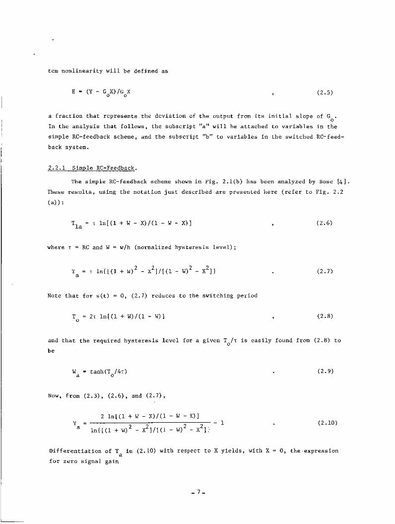
t e m n o n l i n e a r i t y w i l l be de f ined as
a f r a c t i o n t h a t r e p r e s e n t s t h e d e v i a t i o n of t h e ou tpu t from i t s i n i t i a l s l o p e of G . I n t h e a n a l y s i s t h a t fo l lows , t h e s u b s c r i p t "att w i l l be a t t a c h e d t o v a r i a b l e s i n t h e
s imple RC-feedback scheme, and t h e s u b s c r i p t "b" t o v a r i a b l e s i n t h e swi tched RC-feed-
back system.
0
2.2 .1 Simple RC-Feedback.
The s imple RC-feedback scheme shown i n F ig . 2 . l ( b ) h a s been ana lyzed by Bose [ 4 ] .
These r e s u l t s , u s ing t h e n o t a t i o n j u s t descr ibed are p resen ted h e r e ( r e f e r t o F ig . 2.2
( 4 ) :
Tla = T l n [ ( l + W - X ) / ( 1 - W - X)]
where T = RC and W = w/h (normalized h y s t e r e s i s l e v e l ) ;
Note t h a t f o r s ( t ) = 0, (2.7) reduces t o the swi t ch ing pe r iod
To = 2.r l n [ ( l + W)/(1 - W)] 9 (2 8 )
and t h a t t h e r e q u i r e d h y s t e r e s i s l e v e l f o r a g iven to/^ i s e a s i l y found from (2.8) t o
b e
Wa = t a n h ( T o / k )
Now, from (2 .3) , (2.61, and (2.71,
(2 .10)
D i f f e r e n t i a t i o n of Y i n (2.10) wi th respect t o X y i e l d s , w i th X = 0, t h e expres s ion
f o r z e r o s i g n a l g a i n a
- 7 -

It should be observed from ( 2.7) that for full modulation (X = X = 1 - W), m the period T is infinite (system not oscillating). > X 1. Xm the system out- put remains in the high (or low) state and Y = 2 1. An expression for system nonlin-
earity at full modulation (worst case) can be obtained by substitution of (2.11) into
(2.5) with Y = 1, X = X . Hence:
For -X a m -
m
(2.12)
2.2.2 Modified RC-Feedback.
A modification of the simple two-state modulator consists of circuitry that
causes the feedback voltage to reset to zero each time the output changes state. It
will be shown that this system has a higher gain, improved linearity (compared to the
previous system having the same hysteresis characteristic), and a smaller change in
frequency as a function of the modulating signal. From the waveform diagram for this
system shown in Fig. 2.2(b), it can be seen that
Tlb = T ln[l/(l - W - X)]
2 2 Tb = T ln{l/[(l - W) - X ] I
For s(t) = 0 , (2.14) reduces to
To = 2 T ln[l/(l - W)]
from which
Y (2.13)
(2.14)
(2.15)
(2.16)
The normalized average value of the output can be written, from (2.3), (2.13) and
(2.14) as
(2.17)
- 8 -

The derivative of the normalized output with respect to the input, with X = 0 , is
For the switched feedback system it can be seen from (2.13) and (2.14) that
when X = X = W, full modulation occurs, since T
Y = 1. It is interesting to note that the period of oscillation at full modulation
is finite. The worst-case nonlinearity figure (full modulation) is obtained as be-
fore by substituting (2.18) into (2.5), with X = X Y = l. Hence
= Tb, and the output level is m lb
m’
Emb = [(l - W)/W]ln[l/(l - W)] - 1 (2.19)
2.2.3 Synchronous Operation.
It has been remarked that the two-state modulator with simple RC-feedback exhi-
bits poor linearity due to the exponential nature and the variation in duty cycle of
the feedback signal.
ing the switching signal, f(t), from an external generator as in Fig. 2.l(a).
comparison, however, instead of being a triangular wave, f(t) will be the same as that
produced by the feedback system when s(t) = 0 . Typical waveforms for this process are
shown in Fig. 2.2(c).
given by (2.8). Comparison of results obtained from synchronous operation (with expo-
nential switching signal) and operation of the RC-feedback system should then indicate
if performance is improved by elimination of the variation in duty cycle.
The duty cycle (and period) variation may be eliminated by supply-
For
In addition, the switching period will be set equal to the T 0
The operation of the synchronous pulse-width modulator may be explained as
follows (refer to Fig. 2.2(c)): when the sum of the input signal s(t) and the switch-
ing signal f(t) is positive, the output y(t) is at level + h; when the sum is negative the output is at level -h.
feedback system having a normalized hysteresis level W, the analysis yields
With the period T in (2.3) equal to the T for a linear 0
for the normalized output and
for the zero-signal gain.
- 9 -
(2.20)
(2.21)

Now, maximum modulation occurs for X = X = W, and from (2.5) and (2.21), with m X = X and Y = 1, the expression for maximum system nonlinearity is found to be m
Table 2.2 summarizes calculations of gain and nonlinearity made for the worst
case, X = X (full modulation). It is seen that nonlinearity (as defined in (2.5)) with switched feedback is about one-half that for the linear feedback system. This
result is somewhat deceiving since the gain of the modified system is significantly
higher.
the linear feedback system for each value of W , nonlinearity figures and period varia-
tion are reduced considerably.
m
If signal feedback is added to this system to reduce the gain G to that of
The results of digital computer calculations are best
- 10 -
2.3 Comparison of PWM Systems.
A meaningful comparison between the simple and modified feedback systems can
be made by assuming the same hysteresis characteristic for each system. In this case,
however, each configuration requires a different ratio T I T , but adjustment of T allows
for operation with the same fundamental zero-signal period T . An important character-
istic of the modulator with switched feedback is that the period of oscillation does
not vary so widely with modulation level. Table 2.1 lists some calculations of the ra- tio T/T
for X = X is infinite.
0
for signal levels X = .9Xm and X = X
m
for the two systems. Note that T / T m a o
TABLE 2 . 1
Comparison of period variation with signal level for pulse-width modulation systems,
W Ta/To Tb/To Ta/To Tb/To
x = x mb x = .9x x = .9x x = x ma mb ma
.1
.2
. 3
. 4
3.19
2.50
2.12
1.89
1.05
1.13
1.22
1 . 4 4
1.06
1.15
1.29
1.57

(a ) W = . 2 F
1 . 0
.8
.6
. 4
. 2
0 0 . 2 .4 .6 .8 1.0
(b) W = .4 F,Y
1 . 0
.8
.6
. 4
. 2
0 0 . 2 . 4 .6 .8 1.0
F i g . 2 . 3 Normalized average ou tpu t and swi t ch ing f requency v e r s u s
normalized i n p u t f o r two-state modulator (Y F ) and
modif ied two-s ta te modulator (Y F ) w i t h s i g n a l feedback
f o r e q u i v a l e n t power ga in , f o r ( a ) W = . 2 , (b) W = . 4 .
a’ a
b y b
x
X
- 11 -

TABLE 2.2
w
.1
.2
.3
.4
Comparison of zero-signal gain and nonlinearity at full modulation for pulse-width modulation systems
Goa
1.01
1.03
1.06
1.12
Gob
10.6
5.60
3.99
3.26
9.97
4.93
3.23
2.36
9.4
21.5
34.5
48.8
% Emb
5.5
10.8
16.5
23.1
% Emc
0.2
1.2
3.2
5.9
shown by the graphical comparison illustrated in Fig. 2.3 for typical hysteresis levels.
A significant improvement in linearity, dynamic range and frequency stability can be
observed with the modified RC feedback system.
Calculations for synchronous operation are shown in Table 2.2 in columns
headed G and % E . It should be recognized that the zero-signal switching wave-
form is the same as that produced by the corresponding simple RC-feedback system.
Gain is significantly higher, being nearly as high as that given for the switched
feedback case. The nonlinearity figures are much lower than either of the two feed-
back schemes. It is interesting to note that in a synchronous system deviations from
linearity due to a nonlinear switching waveform tend to be minimized when that wave-
form is made up of equal, symmetrical rising and falling segments. This is an impor-
tant fact when the relative complexity of generation of a linear sawtooth is considered.
oc mc
To summarize, it has been shown that performance of a simple two-state
pulse-width modulator can be improved considerably by use pf a modified feedback net- work. However, the properties of a synchronous modulator are the best of the three
types, even with an exponential switching signal. There is, of course, no shift in
switching frequency with input signal and a very high degree of modulation is obtain-
able.

111. Switching Amplifier Design
Distortion - Oscillator Analyzer
During the first six months of this grant several practical switching amplifi-
In the following discussion the switching amplifier ers were designed and evaluated.
is considered in two sections: (a) a switching circuit that creates a two-state pulse-
width modulated (PWM) signal from the low frequency input s(t), and (b) the power
stage that amplifies the two-state PWM signal and drives the low-pass load. A block
diagram of the amplifier and test apparatus is shown in Fig. 3.1.
In order to present a meaningful comparison of the switching schemes employed,
the power stage, supply levels and load were the same in each configuration. The max-
imum power obtainable from this amplifier is about two watts. The value is determined
from
Low-pass
Filter
P = [V cc - VCe(SAT)lL/2%
+"CF Power Stage (b) I , Y(t) (Two-State) ' Ph'M
I I Switching
I I
L s
I Circuit (a) PWM
(3.1)
Low-pass
Load
-v --
Switching Amplifier 1 ----------- r--- c I
7 = A s(t) V
Fig. 3.1 Switching amplifier test configuration.
- 13 -

where :
Vcc = 15 volts (power supply voltage),
V (SAT) 2 0.3 volts (output transistor saturation drop),
% = 50 ohms (resistive component of load).
Considerable design effort was expended in attempting to maximize voltage gain
ce
(Av), power gain ( A ) , efficiency and gain linearity.
to such performance criteria as step response, overload recovery, temperature stabili-
ty and output distortion (including IM distortion).
quite promising and indicate that a switching amplifier can be used as an efficient
Careful attention was given P
The results of this work are
the following loads:
Gimbal torquers
Accelerometer coils
Gyro wheels
Gyro heating elements
AC and DC servo motors Tape recorder heads
Loudspeakers
Relays and solenoids,
3.1 Power Stage Considerations.
The design of power stages for linear amplification is well documented in the
literature. However, the performance of linear power stages suffers from an efficien-
cy limitation. One of the major advantages of the use of switching amplifiers is the
high efficiency inherently obtainable. Consider the complementary (two supply) power
amplifier of Fig. 3.2: here only 0 . 3 volts (V (SAT)) out of the 15 volt supply does not appear across the load. This represents only a 2% reduction in efficiency. If
high speed power transistors are used, active-region switching losses can be kept be-
low 10% of the rated power output.
a 10% loss, and, if switching circuit losses are below 10% an overall efficiency in
the neighborhood of 75% can be obtained. This figure is significantly higher than
the practical efficiency attainable with a class B linear amplifier.
ce
Associated power-stage circuitry contributes about
If only one power supply is available the complementary design is easily modi-
fied into a bridge configuration. (See Fig. 3.3).
3.1.1. Problems of Driving an Inductive Load.
For many important practical applications of the switching amplifier the load

PWM Drive
Fig. 3.2 Complementary two-state power stage.
Fig. 3.3 Complementary bridge configuration.
- 15 -

must be inductive. A word of caution is in order concerning magnetic material in the
load. Most iron is quite lossy at high frequency. However, eddy current losses at the switching frequency can be virtually eliminated if ferrite is used instead of iron
laminations.
The inductive load acts as a low-pass filter. However, the induced voltage
across the inductor at the instant of switching could destroy the output transistors.
To prevent this two clamp diodes (D
Fig. 3.4(a) shows the waveforms of the output drive and the load (ripple) voltage for
a 50% duty cycle PWM input. When the input duty cycle is other than 50%, most of the
load current flows in one direction. Fig. 3.4(b) shows the effect on the output wave-
form.
and D2 of Fig. 3.2) were added to the power stage. 1
It should be pointed out that the speed of the output transistors must be high
to minimize the large currents which flow because of the differences in the turn-on
and turn-off times. During a transition both output transistors can be on for a time
equal to this difference.
3.1.2 Choice of Switching Frequency.
Because the switching frequency limits the useful bandwidth of the amplifier
it should be chosen as high as possible consistent with the frequency response of the
power transistors.
50, then f 2 2mc. This figure corresponds to an output rise time of about 0.17 PS,
based on a first-order step response. During this time the transistor is operating
within its active region. In order to minimize the overall effect of high dissipa-
tion in the active region, the period of the output should be chosen at least ten
times greater than 0.34 p s (two transitions per period), which corresponds to a maxi-
mum switching frequency of nearly 300 kc.
For example, if the output transistors have an f = 100 mc and hfe= T
B
Transistors capable of switching the currents associated with a 2 watt load
can be made in either discrete o r monolithic form, with saturation resistances of
less than 2 ohms. This, of course, represents most of the output impedance of the
amplifier.
3.1.3 Amplifier Bandwidth.
The useful bandwidth of an amplifier with f = 300 kc (zero-signal switching 0
frequency) can not be determined until the frequency change with input is considered.
This change for a typical two-state modulator could lower the switching frequency
to about 100 kc at 90% modulation (See Chapter 11).

3 0
n H
rl a 3 + . U
P 3 + U
0
QI ? *d Ll la U 7 a U 7 0
QI rl a a -4 d n
D W
h r l u rl
3 0
a I a P
7- m
3 0
- 17 -
a, rl Q. a .d p: d
v
3 II 3
U 1 .. a QI
7 0 z 4 U

Distortion figures given in Reference [l] pertain to the presence of difference
frequencies between harmonics of the input signal and the switching frequency that
fall within the amplifier band. To keep distortion from this cause within 1%, a ratio
of about 6 to 1 between the lowest switching frequency and amplifier cut-off frequen-
cy should be observed.
The time constant of the inductive load was adjusted accordingly. It should be pointed
out that the distortion just mentioned is not the same as the harmonic distortion
caused by a nonlinear gain characteristic.
larger and will subsequently be considered.
Hence, the useful amplifier bandwidth should be about 17 kc.
This latter distortion is normally much
The ripple current in the load resistor is quite large because only a 6 db/ octave roll-off is provided by the single L-R combination. Reference to Fig. 3.1
shows a low-pass filter between the load resistor (\) and the distortion analyzer
expressly for the purpose of eliminating ripple from the measurements.
3.1.4 Overload and Step Response.
Any attempt at overmodulation of the switching amplifier results in hard lim-
iting, i. e., switching action ceases and the output remains in one state or the other
for the duration of the disturbance. Overload recovery time is a function of the pro-
pagation and storage delays of the transistors because there are no large energy stor-
age devices requiring discharge time. Similarly, the step response for a small signal
input reflects the delay time of the amplifier, and has rise and fall times dictated by the L-R time constant of the load.
3.2 Self-Oscillating Switching Amplifiers: Hysteresis Type.
The analytical discussion presented in Chapter I1 concerns a two-state modula-
tor with hysteresis and RC feedback. A self-oscillating system operating in this
mode was constructed for evaluation. A block diagram of the system is shown in Fig.
3.5.
A schematic of the Schmitt trigger used is shown in Fig. 3.6. An important
consideration in the operation of the circuit is that a 2N706 transistor is used as
a 6 volt zener diode. The base-emitter breakdown is very sharp and no "keep alive"
current is required.
The output of the Schmitt circuit is inverted by Q and fedback through an 3 RC network. The switching frequency is determined by the RC time constant and the
hysteresis characteristic of the Schmitt. If the trigger input is properly biased, the output is a square wave for s(t) = 0 .
- 18 -

- p w R Power i
Tr igge r S tage
s
Low-pass
Load
Fig . 3.5 S e l f - o s c i l l a t i n g modulator ( h y s t e r e s i s t y p e ) .
0 .1
300 -I- T -
Note:
1 ) A l l r e s i s t o r v a l u e s i n kilohms
2) A l l c a p a c i t o r s i n pico-farads
3 ) A l l t r a n s i s t o r s - 2N706
PWM o u t p u t ( t o Power S tage)
Fig. 3.6 S e l f - o s c i l l a t i n g switching c i r c u i t ( h y s t e r e s i s t y p e ) .
- 19 -

.
3.2.1 Stability Considerations.
Since the switching amplifier is direct coupled, the DC operating conditions
must be carefully controlled. The two trigger levels of the Schmitt circuit shown
in Fig. 3.6 are given by the following expressions:
Vcc - Vce(SAT) RERl 'belRl + RE(Vcc + 'bc)
R + R1 (R1 + RE) (BsAT + 1) Ein(OFF) = [Rs + I + . (3.3)
R + R1 E E
The base-emitter diodes of the transistors used in the Schmitt have a -2.5 mv/OC
temperature coefficient. Stabilization of the firing levels given by (3.2) and (3.3)
can be accomplished over a temperature range in excess of 100" C, by using a 12 volt
zener (+6 mv/"C temperature coefficient) and by chousing R 1, R2, and correctly.
The two firing levels for the circuit shown are 5.6 V (ON) and 4 . 4 V (OFF). The output of Q swings between + 15.0 V and + 8.8 V. Both of the power-supply levels
are assumed to be temperature stable. The feedback waveform must be centered around
+ 5.0 V (Bias in Fig. 3.5) in order to obtain a square-wave output with no input. This bias is provided by R and R. in combination with R the input impedance seen f 1 in' at the base of Q
5
1'
3.2.2 Gain and Distortion.
In the hysteresis amplifier a DC input of 5.6 V produced 90% modulation in the
PWM output waveform.
shown in Fig. 3.2 between 5 15 V, and if V (SAT) = 0.3 V the DC output voltage after ce low-pass filtering) for m = 0.9 (modulation level) would be
If the ichmitt circuit drives a power stage similar to the one
7 = m[V - V (SAT)] = 13.2 V cc ce (3 4 )
The corresponding voltage gain is
A = y/s = 2.4 V ( 3 . 5 )

c
The measured harmonic distortion in the output for s(t) = 5.6 V RMS was 4.8%
occurring mostly as 3rd and 5th. This relatively high distortion could be lowered by
sacrificing gain through additional signal feedback. A substantial amount of feed-
back exists through the same RC network that generates the switching waveform. These
results are compared to other switching amplifier systems in Table 3.2.
3.2.3 Efficiency.
By carefully selecting the bias resistors it was possible to run this amplifier
with 85% efficiency at full load. The zero-signal (standby) power drain was 0.3 watts
which was principally due to the power taken by the drive circuit of the output transis-
tors. This circuit then represents a practical realization of the efficiency figures
discussed in section 3.1.
3.3 Self-Oscillating Switching Amplifiers - Delay Type.
A simple realization of a self-oscillating switching amplifier is shown in Fig.
3.8 (including power stage). The basic amplifier has an input deadband characteristic,
although the inductive load and the output diodes keep the output pulse waveform from
switching to the zero level.
imately 0.6 p s .
switching levels (+ V
stant in the feedback network.
The amplifier also has a significant time delay of approx-
The zero-signal switching frequency therefore depends on the input
- Vbe2 in Fig. 3.7), the time delay (T ) and the RC-time con- bel’ d
Fig. 3.7 Output and summed waveforms.
- 21 -

15K
(Rf 1)
Fig. 3.8 Self-oscillating modulator (delay
with switched RC feedback,
- 22 -
Note 2:
All resistors in kilohms
All capacitors in picofarads
Fig. 3.8 Self-oscillating modulator (delay
with switched RC feedback,
- 22 -
D2
+V cc
1 'bel
'be2
-c -V
cc
LR Load

Analysis of operation is somewhat more complicated than that for the models de-
scribed in Chapter 11.
was decided to try the switched feedback scheme and also to operate the amplifier as a
synchronous modulator. The results are described below.
However, overall operation is sufficiently similar so that it
3.3.1 Stability Considerations.
Careful examination of the circuit presented will show that the Vbe drops of Q, and Q2 must be matched and must track with temperature.
sent.the switching points of the amplifier any unbalance will cause a DC output t o
exist .
Since these levels repre-
There is an obvious DC problem due simply t o the fact that the output transistors
(one NPN and one PNP) can have considerably different saturation drops. Careful atten-
tion must be paid to selecting reasonably matched types. The 2N2297 and 2N3120 have
a Vce(SAT) of 0.2 V and 0.3 V respectively at 200 ma.
a very small percentage of the full output.
The difference voltage represents
3.3.2 Gain and Distortion.
With the switch in position 1 the circuit of Fig. 3.8 takes the form of a two-
state modulator with simple RC feedback. For this system, when the sum of the feedback
signal f(t) and the input signal s(t) reaches the level V
clamping the waveform (See Fig. 3.7) . Because of the propagation delays the output stage
switches T seconds later. With a time constant of T = 2.8 v s in the feedback path
the zero-signal switching frequency is 250 kc, which decreases to 140 kc at a 90% mod-
ulation level. This characteristic of the two-state modulator has been discussed pre-
viously. Voltage gain and distortion at the 90% modulation level (sinusoidal input) are
1.8 and 1.6%, respectively.
Q turns on, effectively bel’ 1
d
The advantages of modifying the exponential feedback signal by clamping to ground
at the start of each output transition have been discussed in Chapter 11. A practical
circuit for accomplishing the clamping is shown in Fig. 3.8, with the switch in posi-
tion 2 . The PWM output is coupled to an inverter, differentiated and fed to PNP and
NPN transistors in parallel across the capacitor in the RC feedback network.
small fraction of the time constant either one of the two transistors (depending upon
the polarity) closes to ground to provide the desired clamping effect. As can be ob-
served from the results shown in Table 3.2, the fractional decrease in switching fre-
quency from f is greater with the modified feedback scheme, contrary to what is pre-
dicted by the analysis of Chapter 11. The gain is higher, as expected, but so is the
For a
0
- 2 3 -

R I Square-wave
Generator
Fig. 3.9 RC Synchronous modulator.
distortion figure. However, measurements were not made for the same zero-signal switch-
ing frequency, and, it should be noted, the mathematical model of this switching ampli-
fier is not as simple as the one discussed in Chapter 11. Some further analytical and
experimental work in this area is anticipated.
In an effort to measure the open-loop characteristics of the amplifier, the feed-
back connection from the amplifier output was opened and a square-wave generator of the
same f and amplitude as produced in the simple RC case was substituted as the drive
for the RC network. (See Fig. 3.9). The voltage gain increased substantially because
the signal feedback path was eliminated. The distortion also increased, and at 90%
modulation was found to be 5.7%. However, after the gain was reduced to the same value
as before by separate signal feedback through the 24K resistor in Fig. 3.9, the total
distortion dropped to 1.5%. This distortion is completely attributable to nonlineari-
ties in the gain characteristic since the switching frequency is fixed by the generator.
In the open-loop configuration, the gain A (not including input attenuation), vo’ was measured to be 6.85 for small-signal input. With this figure it should be possi-
ble to predict the gain for the simple RC - feedback case from the formula
A V = aAvo/(l + BAVo)
where CY = R /(Rin + R f ) , B = R. /(Rin + Rf> and R For values of Rin = 11 K and Rf = 27 K , Av = 1.76, which compares favorably with the
= Rfl + Rf2, as shown in Fig. 3.8- f in f
measured value of 1.8.
- 24 -

3 . 3 . 3 Threshold ing .
An advantage of u s ing an a m p l i f i e r with a deadband c h a r a c t e r i s t i c (See F ig . 3 . 8 )
i s t h a t a mode of o p e r a t i o n c a l l e d th re sho ld ing i s p o s s i b l e .
t u rned on, t h e ou tpu t i s a t z e r o v o l t s and t h e r e i s no feedback t o s t a r t t h e swi t ch ing .
A l l t r a n s i s t o r s are b i a s e d o f f and t h e power d r a i n i s p r a c t i c a l l y ze ro . Swi tch ing
a c t i o n does no t beg in u n t i l t h e s i g n a l i s r a i s e d t o a l e v e l e q u a l t o Vbe(Rf + Rin)/Rf.
By p r o p e r l y des ign ing t h e feedback p a t h ( i . e . , making R l a r g e ) i t i s p o s s i b l e t o have
swi t ch ing cease when t h e i n p u t drops below a p r e s c r i b e d l e v e l , t he reby c o n s t r a i n i n g
t h e o p e r a t i o n so t h a t t h e s tandby power d r a i n is v i r t u a l l y ze ro .
When t h e a m p l i f i e r is f i r s t
f
3 . 4 Open-Loop Swi tch ing Ampl i f ie r .
Because t h e performance of a synchronous system wi th s e p a r a t e s i g n a l feedback
w a s s u p e r i o r t o t h e o t h e r approaches t r i e d , c o n s i d e r a b l e t i m e w a s s p e n t on a des ign
having t h e fo l lowing performance c r i t e r i a :
( a ) Voltage g a i n > 15
(b ) D i s t o r t i o n = 1% a t f u l l modulation
( c ) Wide tempera ture range
(d) F e a s i b l e f o r m i c r o c i r c u i t c o n s t r u c t i o n
( e ) Good t r a n s i e n t and ove r load recovery.
An a m p l i f i e r des igned t o t h e s e s p e c i f i c a t i o n s i s shown i n F ig . 3 . 1 0 .
3.G.1 S e l e c t i o n of Swi tch ing Waveshape.
The use of a s e p a r a t e o s c i l l a t o r requi red i n a synchronous system a l lows an i m -
provement i n g a i n l i n e a r i t y and d i s t o r t i o n because t h e g e n e r a t i o n of a l i n e a r sawtooth
s w i t c h i n g wavefcrm i s p o s s i b l e .
w a s d i c t a t e d by t h e s ta te of t h e a r t i n m i c r o c i r c u i t technology. For example, t h e use
of c a p a c i t a n c e l a r g e r t han a few hundred p i co fa rads o r r e s i s t o r s i n excess of 10 kilohms
i s u n d e s i r a b l e . The des ign i s f u r t h e r r e s t r i c t e d because no p r a c t i c a l i nduc tance is
a v a i l a b l e i n m i c r o c i r c u i t mono l i th i c c o n s t r u c t i o n and only s m a l l v a l u e s are p e r m i s s i b l e
i n h y b r i d c o n s t r u c t i o n .
The des ign of a sawtooth g e n e r a t o r o p e r a t i n g a t 200 kc
A des ign s u i t a b l e f o r r e a l i z a t i o n i n m i c r o c i r c u i t form u t i l i z e s a s t a n d a r d
S c h m i t t - t r i g g e r c i r c u i t w i th feedback, employing a Miller i n t e g r a t o r t o m u l t i p l y t h e
t i m e c o n s t a n t of a s m a l l RC (See Fig. 3.10). This c . i r c u i t y i e l d s a sawtooth of be t -
ter t h a n 1% l i n e a r i t y up t o + 80" C and ,performs s a t i s f a c t o r i l y t o a tempera ture of
+ 120" C. The sawtooth waveform and t h e PWM ou tpu t l e v e l s are shown i n F ig . 3.11. The
c i r c u i t i s s u r e s t a r t i n g and component v a r i a t i o n s w i t h i n t h e r ange of p r a c t i c a l micro-
c i r c u i t l i m i t a t i o n s ( i . e., 2 20% r e s i s t o r s , & 20% c a p a c i t o r s ) show up on ly as changes
- 25 -

> W +
VI E c 4 .ti Y C -4
a, u m VI u 0 U VI -4 VI a, u 4 rl 4
VI ’d m u m w 0 .r( a C -4
a, u m m u 0 U v i u m a m U
rt rl 4
- 26 -

p-5 Q, Collector Waveform
Q,, Collector Waveform
Fig. 3.11 Sawtooth and PWM output signals.
in the initial frequency. This represents no serious limitation in performance.
Shaping of the input-output characteristic of a switching amplifier to some
functional specification (e. g., logarithmic) should be possible by properly shaping
the switching waveform.
for this purpose. This aspect of switching amplifier performance is yet to be investi-
gated.
A nonlinear sawtooth is probably the most practical waveform
3 .4 .2 Differential Amplifier.
In order to provide the highest gain, the hysteresis of the crossover detection circuit (trigger circuit) should be very small, as should the amplitude of the sawtooth.
With this in mind, a high gain differential amplifier was designed. The input change
(at sawtooth terminals) required to move the output transistor from saturation to cut- off is 0.1 V. If the transition time is limited to 10% of the period, the minimum
sawtooth amplitude must be 1.0 V (peak-to-peak).
The reference level for the differential amplifier is obtained by RC filtering
the sawtooth to insure the same DC level on both sides regardless of the temperature change. Another approach to obtaining the reference level, more compatible with micro-
circuit design requirements, is shown in Fig. 3.10 with the switch in position 2 . Since
no large L ' s
verting it and summing the inverted waveform with the original (hum bucking). The
resulting ripple in the linear range of the waveform was reduced to less than 50 mv p-p,
but even this was enough to increase the distortion significantly.
or C's are permitted, the removal of the sawtooth is accomplished by in-
A small amount of
- 27 -
additional filtering is accomplished by using the first transistor stage on the refer- ence side of the differential amplifier as a modified Miller integrator, but more work
is required on this approach before it becomes useful.
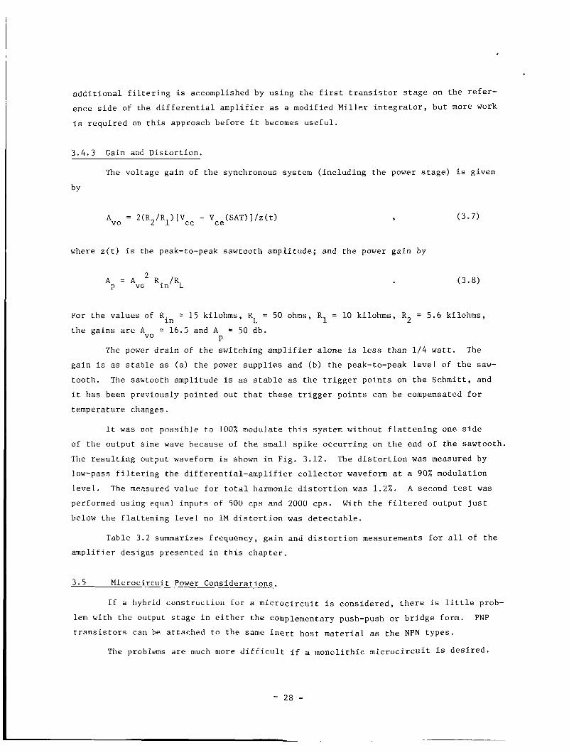
3.4.3 Gain and Distortion.
The voltage gain of the synchronous system (including the power stage) is given
(3.7)
where z(t) is the peak-to-peak sawtooth amplitude; and the power gain by
2 A = A,, Rin/RL P
For the values of R
the gains are A 16.5 and A = 50 db.
2 15 kilohms, R = 50 ohms, R = 10 kilohms, R2 = 5.6 kilohms, in L 1
P vo
The power drain of the switching amplifier alone is less than 114 watt. The
gain is as stable as (a) the power supplies and (b) the peak-to-peak level of the saw-
tooth. The sawtooth amplitude is as stable as the trigger points on the Schmitt, and
it has been previously pointed out that these trigger points can be compensated for
temperature changes.
It was not possible to 100% modulate this system without flattening one side
of the output sine wave because of the small spike occurring on the end of the sawtooth.
The resulting output waveform is shown in Fig. 3.12. The distortion was measured by
low-pass filtering the differential-amplifier collector waveform at a 90% modulation
level. The measured value for total harmonic distortion was 1 . 2 % . A second test was performed using equal inputs of 500 cps and 2000 cps. With the filtered output just
below the flattening level no IM distortion was detectable.
Table 3.2 summarizes frequency, gain and distortion measurements for all of the
amplifier designs presented in this chapter.
3.5 Microcircuit Power Considerations.
If a hybrid construcLion Lor a microcircuit is considered, there is little prob-
lem with the output stage in either the complementary push-push or bridge form.
transistors can be attached to the same inert host material as the NPN types. PNP
The problems are much more difficult if a monolithic microcircuit is desired.
- 28 -

s(t) = 0
- - - s(t) = 1 . 5 ~ p-p
I
Fig. 3.12 Modulation limits of PWM output
Here, PNP transistors can not (without great difficulty and some loss in reliability)
be fabricated on the same substrate with NPN units. A circuit representing a reason-
able solution to this problem is shown in Fig. 3.13 The drive for this amplifier
is assumed to be a single-ended PWM signal such as the output of the synchronous am-
plifier of Fig. 3.10. Notice the use of MOS field-effect transistors (p-channel deple-
tion type) to provide the current drive to the top pair of transistors.
Diodes D and D provide the gating to alternately switch the top transistors 1 2 dependkg on which one of the lower pair is conducting. Even though this circuit has
not been completely evaluated it can be seen that the efficiency will be substantially
lower than a push-push connection due to the fact that there are two transistors and
one diode in series with the load. This could account for as much as a 13% loss in
power output. It should be pointed out that the output impedance for the bridge cir-
cuit is in the 5 ohm range, and that this value would be somewhat higher in a monolithic
design due to the top contact problem on the power transistor cellector.
Other modifications to this circuit along the lines of a balanced drive for all
four power transistors are now under consideration and will be presented in the final
report. This drive could be obtained simply by adding a collector resistor to Q of
Fig. 3.10. 9
3.5.1 Microcircuit Practicality.
There is little question about the use of hybrid microcircuit construction as
a practical way to fabricate either linear or switching amplifiers for low-pass loads
such as those already memtioned. Hybrid techniques are better suited to the small-
quantity production anticipated and in many cases the component tolerances can be
better controlled. Furthermore, the breadboarding job is vastly simplified. However,
the designs undertaken on this grant have been directed toward a monolithic approach
which, it is felt, represents the best realization for space electronic systems.
The question of manufacturing feasibility for the most complex configuration
presented here can be answered by considering two restrictions: (a) power dissipation,
- 29 -

II; l-l
I 1
b u u
P +
I I

(b) ch ip s i z e . Assuming t h e wors t e f f i c i e n c y t o be 75%, t h e 2 w a t t a m p l i f i e r would
r e q u i r e t h a t t h e package be capable of d i s s i p a t i n g 0 .5 w a t t s a t e l e v a t e d t empera tu res .
This can be done w i t h a w e l l hea t - s inked TO-5 case.
Reference t o Table 3 . 1 shows a reasonable component v s . c h i p area r e l a t i o n s h i p
f o r present -day technology i n mono l i th i c s . The areas p resen ted i n c l u d e t h e i s o l a t i o n
space around t h e components. With t h i s t a b l e , c a l c u l a t i o n s f o r t h e synchronous modula-
t o r of F ig . 3 . 1 0 and power s t a g e of F ig . 3 . 1 3 , i n d i c a t e t h e need f o r an area of about
6000 m i l s 2 ( ch ip s i z e of 60 x 100 m i l s ) . It i s in-
t e r e s t i n g t o n o t e t h a t roughly 213 of t h e a r e a i s t aken up by t h e c a p a c i t o r s and power
t r a n s i s t o r s .
2 This i s not a t a l l unreasonable .
There are, of cour se , many o t h e r s u b t l e problems i n m i c r o c i r c u i t des ign which
must s t i l l be cons idered b u t t h e r e i s nothing deemed insurmountable . I n f a c t , i t i s
hoped t h a t a t l eas t one of t h e swi t ch ing a m p l i f i e r des igns p re sen ted i n t h i s c h a p t e r
can be r e a l i z e d i n mono l i th i c i n t e g r a t e d form b e f o r e t h e end of t h i s g r a n t p e r i o d .
- 3 1 -

TABLE 3.1
TYPE
Diode
T r a n s i s t o r
R e s i s t o r
AREA OF INTEGRATED COMPONENTS
SPECIFICATION CHIP AREA ( I N C L U D I N G ISOLATION)
2 (10 mA) 17 m i l s
2 A (10 mA, 20R) 32 m i l s
B (10 mA, 15R) 120
D (1200 mA, 2 R ) 1200 I 1
C (400 mA, 2R) 600
(2 20%)
1009
3009
600R
1kR
2kR
3kR
5kR
lOkR
2 6 m i l s
7 I t
9
12 I '
20
28 I '
45 I '
86
Capac i to r (50 V) 100 pf 460 m i l s '
R e s i s t o r pathwidth = ( 0 . 8 m i l )
Minimum s p a c i n g between components = ( 0 . 4 m i l )
p (Sheet r e s i s t i v i t y ) = 150R/o (base r e g i o n )
- 3 2 -

*
1
TABLE 3.2
COMPARISON OF DIFFERENT TYPES OF
SWITCHING AMPLIFIERS
Distortion(%)** AV*
TYPE fo (kc) frnW Modulation (%)
1 250 140 90 1.8 1.6
2 (a) 330 120 90 3.5 5.6
2 (b) 330 250 90 2.4 1.6
3 (a) 250 250 90 5.1 5.7
3 (b) 250 250 90 1.8 1.5
3 ( c ) 250 250 90 5.3 2.0
4 280 100 85 2.4 4 .8
5 (a) 200 200 90 16.5 1.2
5 (b) 200 200 90 16.5 5.5
1 2(a) - Same as 1 with switched feedback 2(b) - Same as 2(a) with signal feedback
3(a) - Open loop with square-wave drive for RC 3(b) - Same as 3(a) with signal feedback
3(c) - Same as 3(a) with switched feedback
4
5(a) - Synchronous modulator with sawtooth 5(b) - Same as 5(a) with ''hum bucking" circuit.
- 'ITd:' amplifier with 1.2 V deadband
- Hysteresis Amplifier with 1.2 volts of hysteresis
NOTE :
*Small signal including power stage
**Corrected for source distortion and not including ripple at switching frequency.
- 33 -

IV. Reliability Considerations
4.1 Conventional Reliabilitv Theory.
The conventional approach to reliability theory is based on probability theory
and is usually binary in nature. The individual elements have only two states: oper-
ational or failed, and the overall system has likewise only two states: satisfactory
and non-satisfactory. Arbitrary limits are set on the performance of individual com-
ponents, above which they are said to be good and below which they are said to have
failed. In the simplest form of the theory (non-redundant) it is considered that the
system fails whenever a component fails. A great deal of judgement is therefore re-
quired to determine the degree of component variation that constitutes a failure.
al curve for reli- The simp
ability,
est form of reliability theory asslimes an exponent
-At R(t) = E I
Q(t) = 1 - R(t)
The unreliability of the parallel system is
A t A2t 3 )(1 - E )(1 - E )...
- 34 -
where R(t), (the reliability) is the probability of a device operating for time t and
A is the failure rate (a constant number).
In a series system (defined as one in which a failure of any one component
causes a failure of the whole system)
Chit R = E .
S , (4.2)
where X A is the sum of the failure rates of all the components. This formula is
widely used in practice to obtain overall system failure rates (and the reciprocal of
the failure rate, the mean time between failure).
i
For a parallel system (defined as one with redundant elements in parallel) it
is more convenient to work with the unreliability
The unreliability of the parallel system is
A t )(I - E A2t )(1 - E 3 )...
- 34 -
(4.3)
(4.4)

where A i s t h e component f a i l u r e ra te , and the cor responding r e l i a b i l i t y i s i
R = 1 - Q = 1 - (1 - c A l t ) ( l - s A Z t ) ( l - E A3t )... P P
(4 .5)
A s can be seen from t h i s formula t h e r e l i a b i l i t y of a p a r a l l e l o r redundant system i s
much g r e a t e r t h a n t h a t of a non-redundant or series system. A s imple e x t e n s i o n can
be made t o i n c l u d e s e r i e s - p a r a l l e l systems.
4.2 R e l i a b i l i t y Based on Performance Degradat ion.
For many problems a b i n a r y t y p e of r e l i a b i l i t y t heo ry is n o t a s a t i s f a c t o r y
I n f a c t , a whole new theo ry i s needed i n which some a s p e c t of t h e performance one.
of an o v e r a l l system i s s u c c e s s i v e l y degraded, r a t h e r t han t h e whole system f a i l i n g .
Such a t h e o r y r e q u i r e s t h e p re sence of many redundant e lements ( a s f o r example i n t h e
human b r a i n ) and probably w a s n o t r e q u i r e d b e f o r e t h e advent of m i c r o e l e c t r o n i c s . It
seems t o b e a p r e r e q u i s i t e , however, f o r the r a t i o n a l des ign of m i c r o e l e c t r o n i c sys-
t e m s . S e v e r a l p o s s i b l e performance c r i te r ia l end themselves t o s u c c e s s i v e deg rada t ion
by component f a i l u r e .
The f i r s t and most obvious c r i t e r i o n is t h e power o u t p u t . I f t h e r e are sever -
a l e lements i n p a r a l l e l i n t h e ou tpu t of an a m p l i f i e r t h e f a i l u r e of one of them s i m -
p l y r educes t h e a v a i l a b l e power ou tpu t . A more s o p h i s t i c a t e d form of t h i s concept i s
t h e feedforward c i r c u i t (Sec t . 4 . 4 ) i n which the f a i l i l r e of any one channel merely re-
duces t h e peak power a v a i l a b l e .
A second performance c r i t e r i o n which can be s u b j e c t e d t o s u c c e s s i v e deg rada t ion
i s t h e bandwidth. I n a d i g i t a l l y sampled system, t h e bandwidth i s a f u n c t i o n of t h e
sampling ra te . I f t h e sampler i s designed so t h a t each sampling p u l s e comes from a
s e p a r a t e e lement , t h e f a i l u r e of any one of them w i l l merely d e c r e a s e t h e o v e r a l l
bandwidth of t h e system.
A cur so ry a n a l y s i s of t h e r e l i a b i l i t y problem makes i t p robab le t h a t t h e b a s i c
c i r c u i t s should be d i g i t a l i n form and tha t t hey should be in t e rconnec ted i n compli-
c a t e d feedback and feedforward conf igu ra t ions .
p r i n c i p a l des ign c r i t e r i o n f o r mic roe lec t ron ic c i r c u i t s may b e t h e c i r c u i t , as opposed
t o t h e component, r e l i a b i l i t y .
Indeed , i t seems p robab le t h a t t h e
4.3 Redundancy: Majo r i ty Voting.
One method of employing redundancy f o r t h e p rocess of c o n t r o l i s i l l u s t r a t e d
- 35 -

.I Channel 1
Fig. 4.1 Majority voting system
0 Channel b 2
w
in Fig. 4.1. This system has the capability of operating without degraded performance
with a failure of any type in any one of the three channels. A system with this char- acteristic is referred to as fail-operational. This feature is achieved by the majori-
ty voting circuit which selects the signal existing in two of the three channels at
the proper control signal and rejects the third signal if it is different. It can be shown that the probability of failure for such a system is approximately
Majority
Voter *
w
2 QR = 34 + Q,
Channel t 3
( 4 . 6 )
where Q is the probability of failure of a single channel and Q is the probability
of failure of the majority voting circuitry. Neglecting, for the moment, the effects
of Q,, it is clear that this technique achieves a remarkable improvement in system re-
liability. For example, if the probability o€ failure of a single channel is one in
a thousand, then the system probability of failure is three in a million. This is be-
cause at least t w o channels of the three must fail in order to have a system failure.
In order for Q, not to substantially degrade the system reliability it must not be
greater than approximately Q . If the majority voting is performed with digital logic, the circuitry is relatively simple. Despite this simplicity, it may have a probabili-
2 ty of failure significantly higher than Q . Consequently, triple redundancy may be
required in the digital logic circuitry so as not to impair system reliability..
M
2
4.4 Redundancy : Analog.
A triple-redundant analog scheme, developed by Autonetics, and called TRISAFE*,
~~ ~~
* Triple Redundancy Incorporating Self-Adaptive Failure Exclusion
- 36 -
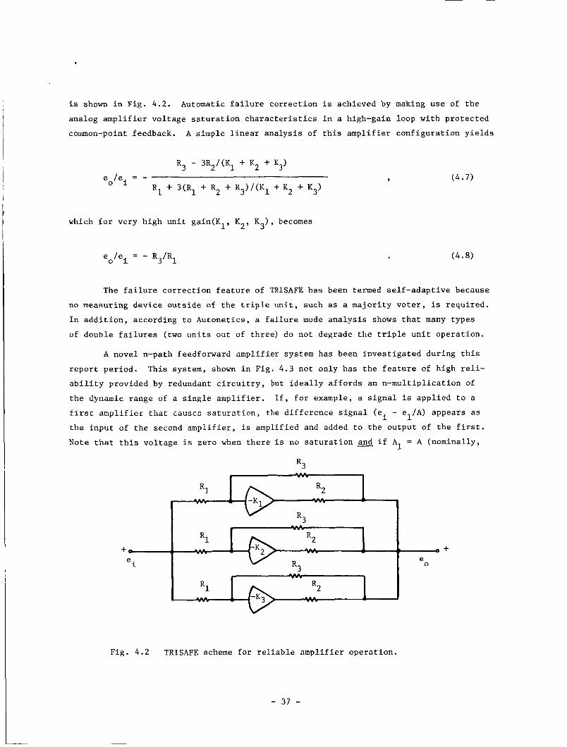
is shown in Fig. 4.2. Automatic failure correction is achieved by making use of the
analog amplifier voltage saturation characteristics in a high-gain loop with protected
common-point feedback. A simple linear analysis of this amplifier configuration yields
e /el = -
K2, K ) , becomes 1’ 3 which for very high unit gain(K
eo/ei = - R /R 3 1
( 4 . 7 )
The failure correction feature of TRISAFE has been termed self-adaptive because
no measuring device outside of the triple unit, such as a majority voter, is required.
In addition, according to Autonetics, a failure mode analysis shows that many types
of double failures (two units oat of three) do not degrade the triple unit operation.
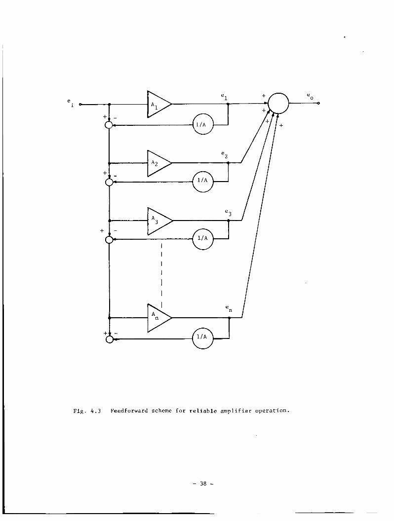
A novel n-path feedforward amplifier system has been investigated during this
report period. This system, shown in Fig. 4.3 not only has the feature of high reli-
ability provided by redundant circuitry, but ideally affords an n-multiplication of
the dynamic range of a single amplifier. If, for example, a signal is applied to a
first amplifier that causes saturation, the difference signal (e - e /A) appears as the input of the second amplifier, is amplified and added to the output of the first.
Note that this voltage is zero when there is no saturation @ if A
i 1
= A (nominally, 1
Fig. 4.2 TRISAFE scheme for reliable amplifier operation.
- 37 -
-+ e 0
e i-
+
Fig. 4 . 3 Feedforward scheme for reliable amplifier operation.

A = A = A = A = A). Subsequent units are similarly connected and the outputs
are summed. This effect is illustrated in Fig. 4.4, where it can be seen that satura- tion in the first two amplifiers does not affect the output.
1 2 3 . - - n
With the feedforward system, if any amplifier should fail the only degradation
in performance is a reduction of l/n in dynamic range. In addition, if all amplifiers
should drift from the nominal gain A by the same amount A, the change in system gain
(also nominally A) is approximately (A/A)" for small A. three-operational amplifier feedforward system is shown in Fig. 4.5. With reference
to the diagram it can be seen that
To illustrate, a detailed
1 A e l i (4.9) e = -
e = -A2(1 - A1!A)ei 2
e3 = -A3[1 - A1/A - (A2/A)l(1 - A1/A)]el
(4.10)
(4.11)
and that
e = e + e + e (4.12) 0 1 2 3
1' For example,
Inspection of (4.9) and (4.10) reveals that if A1 = A2 = A, e2 = e3 = 0 and e Deviation of gain from the value A is compensated for by the redundancy.
if A1 = A2 = A3 = A + A, from (4.9), (4.10), (4.11), and (4.12), the system gain may be
characterized by the expression
= - Ae 0
9 (4.13) 2 3 2 T + AT = -[3(A + A) - 3(A + A) /A t (A + A) /A ]
where T is the transfer ratio
3 (4.14)
and AT is the deviation of that ratio from the nominal value A. Hence, from (4.13)
the fractional change in the transfer ratio is
(4.15) 3 AT/T = (A/A)
- 39 -

I t
Fig. 4.4 Operation of feedforward configuration
when the amplifiers saturate.
- eo
Fig. 4.5 Three-amplifier analog computer representation
of feedforward scheme.
- 40 -

4
i
In summary, it has been shown that the feedforward configuration provides relia- bility through redundancy, dynamic range extension and the advantages of negative feed-
back in maintaining the transfer ratio insensitive to parameter changes. In addition,
it seems feasible to split the frequency band of a signal to be amplified and use am-
plifier sections appropriate to the power and frequency requirements of each of the
sub-bands. The possibilities of the method are quite exciting both for use with ordi-
nary linear amplifiers and with switching amplifiers. Attention is being given to the
development of practical applications of the feedforward method.
- 41 -

V. Conclusions and Research Plans.
The research discussed in this report has been directed toward the application
of advanced circuit concepts for realization of highly reliable and efficient electron-
ic subsystems. Many of the conclusions resulting from the first six months of grant
research are of a tentative nature; however, they form the basis for a continuing re- search effort in the area of reliable solid-state circuits. The main conclusions,
with suggestions for future work, are as follows:
(1) The operation of a two-state modulator with hysteresis and RC feedback
has been shown to be equivalent to the operation of an astable multivibrator (Appendix
A) *
(2) A theoretical development of the operating characteristics of a two-state
modulator with switched RC feedback has been given. Comparison with the simple RC
feedback modulator has demonstrated that the modified system exhibits less variation
in switching period, has a higher gain and a more linear transfer characteristic.
(Chapter 11). Experimental results have generally verified this conclusion (Chapter
111), although, from a practical viewpoint, a new design, not discussed in this report,
shows greater promise (see 5(a), below).
( 3 ) The self-oscillating switching designs described in Chapters I1 and I11
include the signal in the feedback path. On the basis of the work reported here, it
would appear desirable to eliminate the signal from the switching loop and provide
separate signal feedback for linearity improvement. The feasibility of this approach
will be investigated.
( 4 ) It is well-known that a linear-transfer characteristic can be obtained
from a switching amplifier if a perfect triangle or a linear sawtooth is used as a
switching waveform. However, results of an analysis of a synchronous modulator with
exponential segments for a switching waveform show surprisingly small nonlinearity
(Chapter 11).
symmetrical segments tends to be self-compensating, indicating that if a triangular
wave is used, highly linear segments are not necessary.
ear transfer characteristic (a logarithmic relation, for example) should be obtainable
by suitably shaping a sawtooth waveform.
is anticipated.
Investigation leads to the conclusion that a switching waveform having
On the other hand, a nonlin-
Further investigation of these properties
(5) An important conclusion based on the designs presented in Chapter 111 is
that practical realization of a PWM power amplifier combining the features of high

t
. reliability, high efficiency and low distortion is entirely feasible and further, is
compatible with the requirements of present-day integrated circuit technology. Research
will continue in the area of switching amp1.ific.r design with special attention given
to the following:
(a) Development of a self-oscillating, constant switching-frequency design
with high gain and low distortion.
(b) cal inductive loads.
An investigation to determine the magnitude of switching losses for practi-
(c) Introduction of MOS-FETs for high input impedance and improved switching
characteristics.
(d) All NPN power-stage design in a bridge configuration. The use of MOS-FETs
here may realize the benefits of complementary operation in a form easily inte-
grated.
(6) In the area of reliability theory, it is felt that a measure of system
degradation (as a function of component failure) would be very useful in the study of
large-scale systems (Chapter IV). Supporting research will be carried towards this
goal.
(7) It has been shown that a novel feedforward amplifier configuration provides reliability, extension of dynamic range and the advantages of negative feedback.
ther research effort will be directed to development of practical applications of the
method, including the realization of switching amplifiers in the configuration.
Fur-
(8) Two applications of the unijunction transistor for amplitude regulation
Very recent publications in- of an RC oscillator have been described (Appendix B ) .
dicate, however, that field-effect devices may be equally suitable for this applica-
tion.
- 4 3 -

. VI. References.
[l] Carlson, A. W., Scientific Report No. 6, Contract No. AF19(604)-4089, May
1961, Transistor Applications, Inc., Boston, Massachusetts.
[2] Bedford, B. D., "Improvements in and Relating to Electric Amplifying Circuits", U. K. Patent N o . 389,855, March 1933.
[3] Watts, R. J . "Pulse-Width Modulation", U. S . Patent No. 2,556,457, June 1951.
[4] Bose, A. G., "A Two-State Modulating System", Electro-Technology, August,
1964, pp. 42-47
[5] Loos, C. H., "Time Proportional Control", Control Engineering, May, 1965,
pp. 65-70
[6] Clark, L., "New Unijunction Geometries", Electronics, June 14, 1965, pp. 93-
9 7 .
- 44 -
APPENDIX A
Comparison of Two-State Modulator and Multivibrator Operation
The two-state modulator shown in Fig. A.l has been described by Bose [ 4 ] . is here demonstrated that the system operation is equivalent to that of an astable
multivibrator with a modulating signal injected. The notation used in the derivation
is the same as that used by Bose in his paper.
It
A.l System Operation.
In the modulator in kLg. A.l when the signal x, the sum of the modulating signal
2' s and the feedback signal f, exceeds the value w the output y assumes the level h
It remains there until x becomes less than w The
operating point in the x-y plane follows the path indicated by the arrows.
1' at which point y switches to hl.
2
The system is designed to oscillate producing a rectangular waveform at the
output having a period of T ters the frequency and duration of the output pulses in such a way that the average
value of the output is a replica of the time-varying input signal which may then be
recovered by low-pass filtering. The bandwidth of the input signal must be limited
to some small fraction of the lowest switching frequency dependent upon the allowable
distortion.
in the absence of an input signal. The input signal al- 0
W
X -
Fig. A.l Block diagram of two-state modulator.
- 45 -
. Bose has made an analysis of this modulator for the case where the feedback
consists of a single time-constant network cascaded with a delay element. Thus, the
unit-step response of the feedback circuit is taken as 1 - E for t > T
and zero for t < T where Td is the time delay and T is the time constant of the
1, w2 switch points. feedback circuit. The effect of T is to cause x to overshoot the w d He has calculated
-(t - T~)/T d'
d'
The details of Bose's analysis will not be duplicated here.
the time intervals for each of the two states of the output, the switching period, and
the average value of the output signal as a function of the input signal and system
parameters. The results he obtained for the case of symmetrical hysteresis are suffi-
cient for present purposes.
For the case of symmetrical hysteresis, h = -h = h and w = -w2 = w, Bose 1 2 1 derives the following:
- Y =
h h[(R + N)(1 - N)/(R - N)(1 + N)] ln[(R + N)(R - N)/(1 + N)(1 - N)]
2 2 T2 = T ln[(R - N )/(1 - N2)]
and To = 27 In R
where R and N are defined as follows:
Td/T R = 2 h ~ - 1
- In the above, y is the average value of the output signal and represents the useful
output of the system as an amplifier. T is the period of the output pulses with s,
the input signal, equal to zero. 2
A. 2 Equivalent Multivibrator.
The equivalence between Bose's system and an astable or freerunning multivibra-
tor will be shown by considering an astable multivibrator controlled by a single reac-
tive element which for convenience is taken to be a capacitor (Fig. A.2). The ca-

fl -m negative
resistance
V' Jv; + s '
Fig. A.2 (a) Astable multivibrator with modulation. (b) Multi-
vibrator V-I characteristic ( s = 0 ) . (c) Multivibrator
V' - I' characteristic (with modulation).
- 47 -

p a c i t o r sees a t i t s t e r m i n a l s a n e g a t i v e r e s i s t a n c e of t h e o p e n - c i r c u i t s t a b l e o r N
type . c h a r a c t e r i s t i c w i l l be assumed t o be symmetr ica l , i. e , , t h e peak and v a l l e y v o l t a g e s
w i l l be of equal magnitude and i n t h e p o s i t i v e r e s i s t a n c e r e g i o n s t h e s l o p e s w i l l be
i d e n t i c a l and t h e i n t e r c e p t v o l t a g e s e q u a l i n magnitude. Th i s symmetr ica l m u l t i v i b r a -
t o r c h a r a c t e r i s t i c i s shown i n F ig . A.2(b) w i t h t h e p a t h of t h e o p e r a t i n g p o i n t i n t h e
V - I p l a n e marked by ar rows .
To correspond t o Bose ' s symmetr ica l h y s t e r e s i s c a s e t h e n e g a t i v e r e s i s t a n c e
The m u l t i v i b r a t o r may be modulated by app ly ing a s i g n a l s o as t o modify t h e ne-
g a t i v e r e s i s t a n c e c h a r a c t e r i s t i c s e e n by t h e c a p a c i t o r as shown i n F ig . A.2(c) .
V ' - I ' c h a r a c t e r i s t i c i s ob ta ined by combining t h e series combina t ion s and R i n 2 p a r a l l e l w i t h t h e V - I c h a r a c t e r i s t i c .
going from t h e V - I p l a n e t o t h e V' - I ' p l a n e b u t t h e s l o p e s and i n t e r c e p t v o l t a g e s
are modi f ied . The e f f e c t of t h e s i g n a l s i s t o a l t e r t h e i n t e r c e p t v o l t a g e s of t h e
V' - I ' c h a r a c t e r i s t i c and t o cause i t t o s h i f t l e f t o r r i g h t a long t h e I ' a x i s i n
accordance wi th t h e p o l a r i t y and magnitude of s i g n a l s.
The
The peak and v a l l e y v o l t a g e s are unchanged i n
Let T be t h e t i m e t h a t t h e o p e r a t i n g p o i n t i s on t h e e f t hand s i d e of t h e 1 V ' - I' curve i n Fig. A.2(c) , T be t h e p e r i o d of o s c i l l a t i o n of t h e m u l t i v i b r a t o r ,
and T be e q u a l t o R R C/(R1 + R2), t h e t i m e c o n s t a n t of t h e o s c i l l a t o r . 2
1 2
From i n s p e c t i o n of F ig . A.2(c) i t can be s e e n t h a t
T1 = T ln[(V; + V + s ' ) / (V ; - V + s')] P P
by n o t i n g t h a t t h e v o l t a g e a c r o s s t h e c a p a c i t o r i's i n i t i a l l y a t -V when t h e o p e r a t i n g
p o i n t swi t ches t o t h e l e f t s i d e and i n c r e a s e s e x p o n e n t i a l l y toward a f i n a l v a l u e
(Vi + s ' ) b u t swi t ches t o t h e r i g h t s i d e a t T1when t h e v o l t a g e r eaches V . t h e v o l t a g e ac ross t h e c a p a c i t o r w h i l e t h e o p e r a t i n g p o i n t i s on t h e l e f t s i d e i s
(V + V ' + s ' ) ( i - E
P
That i s , P
- t i r ) - Vp w i t h t = 0 t h e moment of s w i t c h i n g t o t h e l e f t s i d e . P I
S i m i l a r l y , t h e t i m e t h a t t h e o p e r a t i n g p o i n t is on t h e r i g h t s i d e of t h e
c h a r a c t e r i s t i c is g iven by
T2 - T = ln[(V; + V - s ' ) / ( V ; - V - s ' ) ] 1 P P
The per iod of o s c i l l a t i o n is o b t a i n e d by add ing e q u a t i o n s (A.6) and (A.7) t o
o b t a i n

To bring the notation into agreement with that of Bose let
R = (Vi + V )/(Vi - V ) P P 9
N = s'/(V; -
Substitution of (A.9) and (A.lO) into (A.6),(A.7) and (A.8) yields
T1 = T ln[(R + N)/(1 + N)] 3 (A. 11)
Y (A. 12) 2 T2 - T1 = 7 ln[(R - N)/(1 - N ) ]
T2 = T ln[(R2 - N 2 ) / ( 1 - N2)] (A. 13)
Equation (A.13) is seen to be identical to ( A . 2 ) derived by Bose.
Suppose that the multivibrator produces an output signal (either by itself
or by controlling a suitable switch) that has the value h during the interval T and
the value -h during the interval (T2 - T1). 1
Then
hT - h(T2 - TI) h ln[(R + N)(1 - N)/(R - N)(1 + N)]
h[(R + N)(R - N)/(l + N)(1 - N)]
1 - Y (A.14) - - Y =
T2
where 7 is the average value of y.
and when N = 0 (no signal, s also zero), (A.13) becomes
Equation (A.14) is seen to be identical to (A.l),
T~ = ~~1 = 2.r In R s = o
9 (A.15)
which is the same as (A.3) given by Bose.
Thus it has been demonstrated that Bose's system is equivalent to modulating
an astable multivibrator, when the feedback contains a single time constant. The
voltage V corresponds to w in Bose's system and the intercept voltage V' corresponds
to h as far as determining time intervals is concerned. With these equivalents and
identifying s' with Bose's s, (A.9) and (A.lO) are the same as (A.4) and (A.5) when
the time delay Td is zero.
P I
Without the time delay considered by Bose, R is a measure
- 49 -

c
of the portion of the exponential used in generating the output pulses. When R is
large a greater portion of the exponential is used and the nonlinearity of the response
is increased. The parameter N represents a normalized signal, the modulation of the
output signal being complete when the magnitude of N is unity.
A multivibrator described by a negative-resistance characteristic that has
unequal peak and valley voltage magnitudes and unequal intercept voltage magnitudes corresponds to Bose's general case.
tance regions are unequal the multivibrator becomes equivalent to what Bose's system
would be if the feedback time constant were to have one value for one state of the
output and a different value for the other state.
If in addition, the slopes in the positive resis-
- 50 -

Appendix B
Oscillator Amplitude Regulation Using the Unijunction Transistor
B.l Amplitude Regulation.
One purpose of automatic amplitude regulation of an oscillator is to maintain
the output at a constant level independent of changes in circuit values, supply volt-
ages, frequency, etc. over reasonable limits. A second important function is to limit operation to the linear region in order to minimize distortion in the output waveform.
An incandescent lamp is frequently used as an amplitude control device in RC
oscillators (such as the Wien bridge oscillator). The lamp is pleced in the circuit in such a way that an increase in oscillator signal amplitude causes the power dissi-
pated in the filament to increase, the temperature to rise, and the filament resistance to increase. If the increase in lamp resistance acts to decrease the oscillator loop
gain, the output of the oscillator can be stabilized at a point where oscillations of
the desired amplitude are sustained. The lag in response of the filament temperature
to a change in power dissipated acts as a filter; the lower frequency limit to the
lamp's usefulness comes when the temperature variation over a cycle of oscillation
results in an unacceptable amount of distortion.
It is the purpose of the discussion to dcmonstrate that the unijunction tran-
sistor may be used instead of the incandescent lamp for oscillator amplitude control.
This device, in addition to providing more reliable operation, is easily integrated
[ 6 ] .
state oscillator circuits.
The following describes two distinct applications of the unijunction in solid-
B.2 The Uniiunction Transistor.
Fig. B.l is a sketch of the Vb2 - Ib2 characteristics of a unijunction transis- tor with IE as a parameter.
constant IE curves changes appreciably with IE; the incremental resistance in this
region, over a range of about 0.4 volts, is a nearly linear, decreasing function of I
It is seen that at low positive voltage the slope of the
E ' Above and below the breakpoints in the low voltage region the incremental resistance
is higher and a decreasing function of IE, but is not nearly so sensitive to IE as in the low voltage region. Fig. B.2 shows a plot of incremental resistance for a 2N489
unijunction transistor over the linear portion of the low-positive voltage region.
In the region beyond the breakpoints, the change in incremental resistance is very
- 51 -

"b2
3
2
2
IE = 0 .3 .6 1 2 3
I I I I
1 2 Ib2
I = E 1 .6 .3 0
Unijunction Characteristic. Fig . B.l "b2 - Ib2
- 5 2 -

Ohms
2000
1000
500
200
100
\
'b2 .02 .05 .1 .2 .5 1 2 5
Fig . B.2 Inc remen ta l r e s i s t a n c e v s . v o l t a g e (Vb2) f o r a 28489 uni -
j u n c t i o n t r a n s i s t o r
much less, perhaps a two-to-one v a r i a t i o n over a range of I from 0 t o 4 mil l i amperes . E The u n i j u n c t i o n may be used t o c o n t r o l ampl i tude i n two d i f f e r e n t ways, by use
of d i f f e r e n t p o r t i o n s of t h e Vb2 - Ib2 c h a r a c t e r i s t i c s .
p o r t i o n of t h e Vb2 - Ib2 curves i n t h e low v o l t a g e r e g i o n (between t h e b r e a k p o i n t s )
i s s u i t a b l e f o r ampl i tude c o n t r o l w i t h t h e u n i j u n c t i o n l o c a t e d i n t h a t p a r t of t h e
c i r c u i t where g a i n is dec reased by a n i n c r e a s e i n r e s i s t a n c e (o the rwise t h e g a i n would
i n c r e a s e at t h e ends of t h e r eg ion be ing used and d i s t o r t i o n would be ex t reme) . Opera-
t i o n o v e r t h a t p a r t of t h e Vb2 - Ib2 curves beyond t h e b r e a k p o i n t s ( e i t h e r quadran t )
i s s u i t a b l e f o r ampl i tude c o n t r o l w i t h t h e u n i j u n c t i o n l o c a t e d i n t h e c i r c u i t s o t h a t
a d e c r e a s e i n r e s i s t a n c e r e s u l t s i n a g a i n r e d u c t i o n .
Opera t ion over t h e l i n e a r
The u n i j u n c t i o n t r a n s i s t o r may b e b i a sed s t a b l y i f t h e emit ter c u r r e n t i s sup-
p l i e d by a c u r r e n t sou rce o r a s o u r c e having a r e s i s t a n c e g r e a t e r t han t h e n e g a t i v e
r e s i s t a n c e s e e n a t t h e emitter. The l i m i t e d f requency r e sponse of t h e u n i j u n c t i o n
a l s o p e r m i t s an a p p r e c i a b l e amount of shunt c a p a c i t a n c e a t t h e emitter wi thou t caus ing
i n s t a b i l i t y . The c o l l e c t o r c i r c u i t of a t r a n s i s t o r i s a s u i t a b l e s o u r c e of emit ter
c u r r e n t b i a s f o r o p e r a t i n g a u n i j u n c t i o n as an ampl i tude c o n t r o l e lement .
- 53 -

B.3 O s c i l l a t o r C i r c u i t s .
F ig . B.3(a) shows a feedback a m p l i f i e r t y p i c a l l y used i n t h e Wien b r i d g e o s c i l -
l a t o r shown i n F ig . B.3(b) . T h i s c i r c u i t w a s employed t o t e s t t h e o p e r a t i o n of t h e
u n i j u n c t i o n t r a n s i s t o r as an ampl i tude c o n t r o l e lement .
pu t r e s i s t a n c e , a low o u t p u t r e s i s t a n c e , and a v o l t a g e g a i n of approximate ly (1 + R 2 1 / R ) .
I n t h e o s c i l l a t o r c i r c u i t of F ig . B.3(b) , when Rs = R = R and Cs = C P P
f i e r g a i n of 3 i s r e q u i r e d t o s u s t a i n o s c i l l a t i o n a t f requency 1 / 2 n R C .
The a m p l i f i e r h a s a h igh in-
= C , a n ampli-
92 Ql
0
P V I"
t "1 I
Feedback
R P
F i g . B.3 (a) T y p i c a l feedback a m p l i f i e r used i n ( b ) Wien-
Bridge o s c i l l a t o r
I
- 5 4 -

39 73, + 4.4v
+ 3v
Note: A l l resistor values in kilohms, all capacitor values in microfarads
Fig. B . 4 Wein-Bridge Oscillator circuits showing two ways of using
unijunction transistors for amplitude control.
- 55 -

In Fig. B.4(a) and (b), two Wien-bridge oscillator circuits, adjustable by
ganged potentiometers over the range of 60 to 600 cps. are shown. The circuits are
essentially the same except for the manner in which the unijunction transistors are
used to regulate oscillator amplitude.
fied, filtered and compared to a reference V (shown as 1.4 volts). This error signal
is amplified to provide the emitter current needed by the unijunction transistor to
maintain the amplitude constant. If the gain of the amplitude control loop is suffi-
ciently high, the peak-to-peak amplitude of the oscillations equals 2V neglecting
voltage loss in D2 and V drops in control loop transistors. In the circuit of Fig.
B.4(a), the peak-to-peak amplitude of the output was held constant at 4 volts, and in the circuit of Fig. B.4(b) at 6.4 volts, with V of 1.4 volts.
In each circuit, the output voltage is recti-
R
R’
be
R
In Fig. B.4(a) the unijunction transistor is operated in the first quadrant
2 above the breakpoints in the V in the circuit of Fig. B.3(a). Q4 in accordance with the error signal must increase to reduce the gain (for amplitude
regulation) of the amplifier.
- Ib2 curves and functions as part of resistance R b2 The emitter current supplied to the unijunction by
In Fig. B.4(b) the unijunction is ofierated in the low voltage region between
the breakpoints of the Vb2 - Ib2 curves shown in Fig. B.l and is connected to form part of resistance R in the amplifier of Fig. B.3(a). Here the emitter current sup-
plied to the unijunction must be reduced by the error signal to reduce amplifier gain
and oscillator output.
1
The unijunction transistor functions equally well in both methods of control
shown in Fig. B.4. With 2N489 transistors the B1 and B 2 connections can be interchanged
with little change in operation except that in the circuit of Fig. B.&(a), the emitter
current level in the unijunction approximately doubles.