Embed Size (px)
Citation preview

October 2011 Doc ID 18349 Rev 1 1/24
24
ST7590Narrow-band OFDM power line networking
PRIME compliant system-on-chip
Features Fully integrated narrow-band power line
networking system-on-chip
High performing DSP engine with embedded turn-key firmware for Orthogonal frequency division multiplexing (OFDM) modulation, featuring:– 96 sub-carriers in CENELEC A band– BDPSK, QDPSK, 8DPSK programmable
modulations– Programmable bit rate up to 128 kbps– Convolutional coding and Viterbi decoding– Signal to noise ratio and channel quality
estimation– Full PRIME compliant PHY
On chip peripherals:– Host controller UART/SPI interface– I2C/SPI external data memory interface – High speed SRAM controller for optional
external SRAM program code execution– Watchdog timer
On chip 128 bit AES encryption HW block
Fully integrated analog front end: – ADC and DAC– High sensitivity receiver– High linearity transmitter with intelligent
gain control
Fully integrated power line driver – Up to 1 Arms, 14 Vpp single ended– Configurable active filtering topology– Ultra low distortion – Embedded temperature sensor – Current control
3.3 V or 5 V I/O digital I/O supply
Integrated 5 V and 1.8 V linear regulators for AFE and digital core supply
8 V to 18 V line driver power supply
Suitable for applications compliant with EN50065 and FCC part 15 specifications
-40 °C to +85 °C temperature range
QFN48 7x7 (ST7590) and TQFP 100 14x14 (ST7590T) exposed pad package options
ApplicationPRIME compliant smart metering and smart grid applications.
DescriptionST7590 is the first complete Narrowband OFDM power line communication system-on-chip made using a multi-power technology with state of the art VLSI CMOS lithography. The ST7590 is based on dual core architecture to assure outstanding communication performance with a very high level of flexibility and programmability for either open standard or fully customized implementations.
QFN-48(7 x 7 mm)
www.st.com

Contents ST7590
2/24 Doc ID 18349 Rev 1
Contents
1 Device description . . . . . . . . . . . . . . . . . . . . . . . . . . . . . . . . . . . . . . . . . . 3
2 Pin connection . . . . . . . . . . . . . . . . . . . . . . . . . . . . . . . . . . . . . . . . . . . . . . 4
3 Maximum ratings . . . . . . . . . . . . . . . . . . . . . . . . . . . . . . . . . . . . . . . . . . . . 8
3.1 Absolute maximum ratings . . . . . . . . . . . . . . . . . . . . . . . . . . . . . . . . . . . . . 8
3.2 Thermal data . . . . . . . . . . . . . . . . . . . . . . . . . . . . . . . . . . . . . . . . . . . . . . . 8
3.3 Electrical characteristics . . . . . . . . . . . . . . . . . . . . . . . . . . . . . . . . . . . . . . . 9
4 Analog front end (AFE) . . . . . . . . . . . . . . . . . . . . . . . . . . . . . . . . . . . . . . 14
4.1 Reception path . . . . . . . . . . . . . . . . . . . . . . . . . . . . . . . . . . . . . . . . . . . . . 14
4.2 Transmission path . . . . . . . . . . . . . . . . . . . . . . . . . . . . . . . . . . . . . . . . . . 15
4.3 Power amplifier . . . . . . . . . . . . . . . . . . . . . . . . . . . . . . . . . . . . . . . . . . . . . 15
4.4 Thermal shutdown and temperature control . . . . . . . . . . . . . . . . . . . . . . . 15
4.5 Zero-crossing detector . . . . . . . . . . . . . . . . . . . . . . . . . . . . . . . . . . . . . . . 16
4.6 One time programmable (OTP) memory array . . . . . . . . . . . . . . . . . . . . . 16
4.7 Power management . . . . . . . . . . . . . . . . . . . . . . . . . . . . . . . . . . . . . . . . . 16
4.8 Clock management . . . . . . . . . . . . . . . . . . . . . . . . . . . . . . . . . . . . . . . . . 17
5 Application information . . . . . . . . . . . . . . . . . . . . . . . . . . . . . . . . . . . . . 18
6 Package mechanical data . . . . . . . . . . . . . . . . . . . . . . . . . . . . . . . . . . . . 19
7 Revision history . . . . . . . . . . . . . . . . . . . . . . . . . . . . . . . . . . . . . . . . . . . 23

ST7590 Device description
Doc ID 18349 Rev 1 3/24
1 Device description
ST7590 is available in two different package options: TQFP100 and QFN48.
In the TQFP100 package option, order code ST7590T, the device comes with a dedicated FW implementing PRIME compliant PHY protocol Layer and a boot loader procedure that enables the IC to boot PRIME MAC, PRIME CL432 Convergence Layer and IEC 61334-4-32 LLC Layer from an external Serial NV memory connected through SPI interface.
In the QFN 48 package option, ST7590 comes with a dedicated FW implementing the full PRIME protocol stack (PHY, MAC and Convergence Layer), so without the need for external memories to run the protocol.
The on-chip analog front end, featuring analog to digital and digital to analog conversion and automatic gain control, plus the integrated power amplifier delivering up to 1 Arms (typical) output current, makes the ST7590 the first complete Narrowband OFDM power line communication system-on-chip ideal for PRIME compliant applications.
An HW 128-bit AES encryption block with PRIME compliant management is available on chip when secure communication is requested.
Line coupling network design is also extremely simplified, leading to a very low cost Bill Of Material.
Safe operations are assured while keeping power consumption and distortion levels very low, so making ST7590 an ideal platform for the most stringent application requirements and regulatory standards compliance.
Figure 1. ST7590 block diagram
Ouptut CurrentControl
ThermalManagement
P_ROM X-RAM Y-RAM
DSPEngine
HardwareAccelerators
Line Driver
PHY Processor
GAIN BPF
BPFADCPGA
DAC
PROGROM
OTP
8051
CORE
UART/SPI0
10 GPIO
JTAGWatchdog
3 Timers 2 Interrupts
AES128
DATARAM
NVM SPI SRAM Contr.
PROTOCOLControllerAFE
POWER Management CLOCK ManagementZero Crossing Detector
PA_IN+
PA_IN-
CLOptional ExternalFLASH Memory
Optional ProgramSRAM
PA_OUT
TX_OUT
RX_IN
VCC(8-18V)
VCCA(5V)
VDDIO(3.3/5V)
VDD(1.8V) ZC_IN VDD_PLL XIN XOUT

Pin connection ST7590
4/24 Doc ID 18349 Rev 1
2 Pin connection
Figure 2. TQFP100 pin connection
Figure 3. QFN48(a) pin connection
a. The QFN48 package option does not allow the connection with an external memory; in this configuration the ST7590 will run the code present in the embedded ROM only.

ST7590 Pin connection
Doc ID 18349 Rev 1 5/24
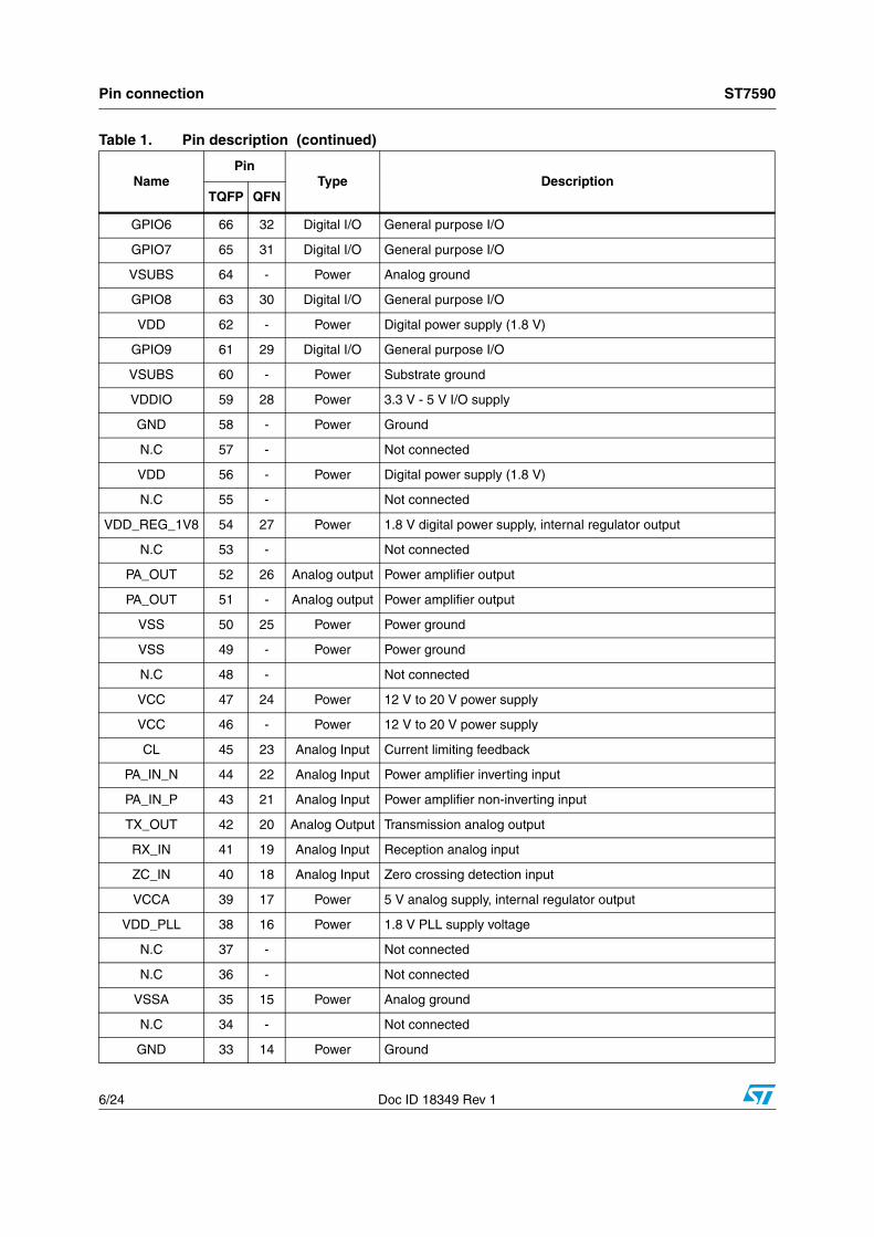
Table 1. Pin description
NamePin
Type DescriptionTQFP QFN
SCLK0 100 48 Digital input SPI0 serial clock
SSN0 99 47 Digital input SPII0 slave select (active low)
VDD 98 46 Power Digital power supply (1.8 V)
GND 97 45 Power Ground
MISO1 96 44 Digital input SPI1 data in
MOSI1_SDA 95 43 Digital I/O SPI1 data out, I2C data in (I2C always selected at boot)
SRAM_A15 94 - Digital output External SRAM Address
VDDIO 93 - Power 3.3 V - 5 V I/O supply
SRAM_A16 92 - Digital output External SRAM Address
SCLK1_SCL 91 42 Digital output SPI1 serial clock, I2C serial clock ((I2C always selected at boot)
SRAM_D0 90 - Digital I/O (1) External SRAM data I/O
SRAM_D1 89 - Digital I/O (1) External SRAM data I/O
SRAM_D2 88 - Digital I/O (1) External SRAM data I/O
SRAM_D3 87 - Digital I/O (1) External SRAM data I/O
SRAM_D4 86 - Digital I/O (1) External SRAM data I/O
SRAM_D5 85 - Digital I/O (1) External SRAM data I/O
SRAM_D6 84 - Digital I/O (1) External SRAM data I/O
SRAM_D7 83 - Digital I/O (1) External SRAM data I/O
SRAM_CSN 82 - Digital output External SRAM chip select
SRAM_WEN 81 - Digital output External SRAM write enable
SRAM_OEN 80 - Digital output External SRAM output enable
GPIO0 79 41 Digital I/O General purpose I/O
GPIO1 78 40 Digital I/O General purpose I/O
GPIO2 77 39 Digital I/O General purpose I/O
VDDIO 76 - Power 3.3 V - 5 V I/O supply
GPIO3 75 38 Digital I/O General purpose I/O
N.C 74 - Not connected
GPIO4 73 37 Digital I/O General purpose I/O
N.C 72 - Not connected
GPIO5 71 36 Digital I/O General purpose I/O
VDD_12V 70 35 Power OTP programming voltage (12 V)
VDD 69 - Power Digital power supply (1.8 V)
VDDIO 68 34 Power 3.3 V - 5 V I/O supply
GND 67 33 Power Ground
Pin connection ST7590
6/24 Doc ID 18349 Rev 1
GPIO6 66 32 Digital I/O General purpose I/O
GPIO7 65 31 Digital I/O General purpose I/O
VSUBS 64 - Power Analog ground
GPIO8 63 30 Digital I/O General purpose I/O
VDD 62 - Power Digital power supply (1.8 V)
GPIO9 61 29 Digital I/O General purpose I/O
VSUBS 60 - Power Substrate ground
VDDIO 59 28 Power 3.3 V - 5 V I/O supply
GND 58 - Power Ground
N.C 57 - Not connected
VDD 56 - Power Digital power supply (1.8 V)
N.C 55 - Not connected
VDD_REG_1V8 54 27 Power 1.8 V digital power supply, internal regulator output
N.C 53 - Not connected
PA_OUT 52 26 Analog output Power amplifier output
PA_OUT 51 - Analog output Power amplifier output
VSS 50 25 Power Power ground
VSS 49 - Power Power ground
N.C 48 - Not connected
VCC 47 24 Power 12 V to 20 V power supply
VCC 46 - Power 12 V to 20 V power supply
CL 45 23 Analog Input Current limiting feedback
PA_IN_N 44 22 Analog Input Power amplifier inverting input
PA_IN_P 43 21 Analog Input Power amplifier non-inverting input
TX_OUT 42 20 Analog Output Transmission analog output
RX_IN 41 19 Analog Input Reception analog input
ZC_IN 40 18 Analog Input Zero crossing detection input
VCCA 39 17 Power 5 V analog supply, internal regulator output
VDD_PLL 38 16 Power 1.8 V PLL supply voltage
N.C 37 - Not connected
N.C 36 - Not connected
VSSA 35 15 Power Analog ground
N.C 34 - Not connected
GND 33 14 Power Ground
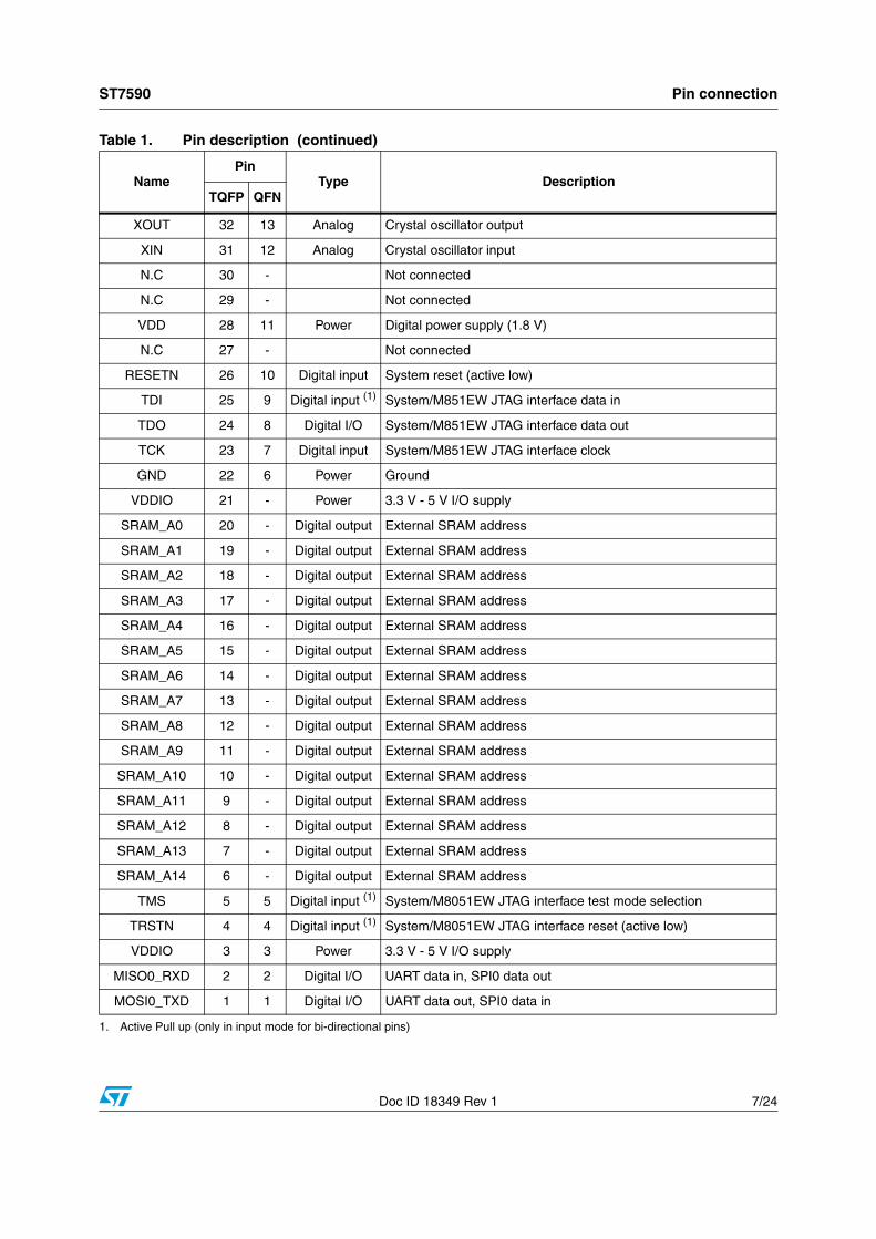
Table 1. Pin description (continued)
NamePin
Type DescriptionTQFP QFN
ST7590 Pin connection
Doc ID 18349 Rev 1 7/24
XOUT 32 13 Analog Crystal oscillator output
XIN 31 12 Analog Crystal oscillator input
N.C 30 - Not connected
N.C 29 - Not connected
VDD 28 11 Power Digital power supply (1.8 V)
N.C 27 - Not connected
RESETN 26 10 Digital input System reset (active low)
TDI 25 9 Digital input (1) System/M851EW JTAG interface data in
TDO 24 8 Digital I/O System/M851EW JTAG interface data out
TCK 23 7 Digital input System/M851EW JTAG interface clock
GND 22 6 Power Ground
VDDIO 21 - Power 3.3 V - 5 V I/O supply
SRAM_A0 20 - Digital output External SRAM address
SRAM_A1 19 - Digital output External SRAM address
SRAM_A2 18 - Digital output External SRAM address
SRAM_A3 17 - Digital output External SRAM address
SRAM_A4 16 - Digital output External SRAM address
SRAM_A5 15 - Digital output External SRAM address
SRAM_A6 14 - Digital output External SRAM address
SRAM_A7 13 - Digital output External SRAM address
SRAM_A8 12 - Digital output External SRAM address
SRAM_A9 11 - Digital output External SRAM address
SRAM_A10 10 - Digital output External SRAM address
SRAM_A11 9 - Digital output External SRAM address
SRAM_A12 8 - Digital output External SRAM address
SRAM_A13 7 - Digital output External SRAM address
SRAM_A14 6 - Digital output External SRAM address
TMS 5 5 Digital input (1) System/M8051EW JTAG interface test mode selection
TRSTN 4 4 Digital input (1) System/M8051EW JTAG interface reset (active low)
VDDIO 3 3 Power 3.3 V - 5 V I/O supply
MISO0_RXD 2 2 Digital I/O UART data in, SPI0 data out
MOSI0_TXD 1 1 Digital I/O UART data out, SPI0 data in
1. Active Pull up (only in input mode for bi-directional pins)
Table 1. Pin description (continued)
NamePin
Type DescriptionTQFP QFN

Maximum ratings ST7590
8/24 Doc ID 18349 Rev 1
3 Maximum ratings
3.1 Absolute maximum ratings
3.2 Thermal data
Table 2. Absolute maximum ratings
Symbol ParameterValue
UnitMin Max
VCC Power supply voltage -0.3 20 V
VSSA-GND Voltage between VSSA and GND -0.3 0.3 V
VDDIO I/O supply voltage -0.3 5.5 V
VI Digital input voltage GND-0.3 VDDIO+0.3 V
VO Digital output voltage GND-0.3 VDDIO+0.3 V
V(PA_IN) PA inputs voltage range VSS-0.3 VCC+0.3 V
V(PA_OUT) PA_OUT voltage range VSS-0.3 VCC+0.3 V
V(RX_IN) RX_IN voltage range -(VCCA+0.3) VCC+0.3 V
V(ZC_IN) ZC_IN voltage range -(VCCA+0.3) VCCA+0.3 V
V(TX_OUT, CL) TX_OUT, CL voltage range VSSA-0.3 VCCA+0.3 V
V(XIN) XIN voltage range GND-0.3 VDDIO+0.3 V
I(PA_OUT)Power amplifier output non-repetitive peak current
5 Apeak
I(PA_OUT)Power amplifier output non-repetitive rms current
1.4 Arms
Tamb Operating ambient temperature -40 85 ºC
Tstg Storage temperature -50 150 ºC
V(ESD)
Maximum withstanding voltage rangetest condition: cdf-aec-q100-002 “human body model” acceptance criteria: “normal performance”
-2 +2 kV
Table 3. Thermal characteristics (1)
1. Typical values.
Symbol Parameter QFN48 TQFP100 Unit
RthJA1 Maximum thermal resistance junction-ambient steady state(2)
2. Mounted on a 2s PCB.
58 50 °C/W
RthJA2 Maximum thermal resistance junction-ambient steady state(3)
3. Mounted on a 2s2p PCB, with a dissipating surface, connected through vias, on the bottom side of the PCB.
32 25 °C/W

Maxim
um
rating
sS
T7590
9/24D
oc ID 18349 R
ev 1
3.3 Electrical characteristicsTA = -40 to +85 °C, TJ < 125 °C, VCC = 18 V unless otherwise specified.
Table 4. Electrical characteristics
Symbol Parameter Test conditions Min. Typ. Max. Unit
Power supply
VCC Power supply voltage 8 13 18 V
I(VCC) RX Power supply current - Rx modeVCCA externally supplied
0.35 0.5 mA
I(VCC) TX Power supply current - Tx mode, no load 22 30 mA
VCC UVLO_TL VCC under voltage lock out low threshold 6.1 6.5 6.95 V
VCC UVLO_TH VCC under voltage lock out high threshold 6.8 7.2 7.5 V
VCC UVLO_HYST VCC under voltage lock out hysteresis 250 (1) 700 mV
VCCA Analog supply voltage Externally supplied -5% 5 +5% V
I(VCCA) RX Analog supply current - Rx mode 5 6 mA
I(VCCA) TX Analog supply current - Tx mode V(TX_OUT) =5 V p-p, No load 8 10 mA
VDD Digital core supply voltage Externally supplied -10% 1.8 +10% V
I(VDD) Digital core supply current 35 mA
I(VDD) Digital core supply current in RESET state 8 mA
VDD_PLL PLL supply voltage VDD V
I(VDD_PLL) PLL supply current 0.4 mA
VDDIO Digital I/O supply voltage Externally supplied -10% 3.3 or 5 +10% V
VDDIO UVLO_TLI/O supply voltage under voltage lock out low threshold
2.25 2.4 2.6 V
VDDIO UVLO_TH I/O supply voltage under voltage lock out high threshold
2.45 2.6 2.8 V
VDDIO
UVLO_HYST
I/O supply voltage under voltage lock out hysteresis
250 mV

Maxim
um
rating
sS
T7590
10/24D
oc ID 18349 R
ev 1
Analog front end
Power amplifier
V(PA_OUT)BIAS Power amplifier output bias voltage - Rx mode VCC/2 V
GBWP Power amplifier gain-bandwidth product 100 MHz
I(PA_OUT)MAX Power amplifier maximum output current 1000 mA rms
V(PA_OUT) TOL Power amplifier output tolerance (2) -3% 3%
V(PA_OUT) HD2 Transmitter output 2nd harmonic distortion VCC=13 V, V(PA_OUT) = 7 V p-p, V(PA_OUT) BIAS = VCC/2, RLOAD=50 Ω see Figure 4
-71 dBc
V(PA_OUT) HD3 Transmitter output 3rd harmonic distortion -68 dBc
V(PA_OUT) THD Transmitter output total harmonic distortion 0.1 %
V(PA_OUT) HD2 Transmitter output 2nd harmonic distortion VCC=18 V, V(PA_OUT) = 14 V p-p,
V(PA_OUT) BIAS = VCC/2, RLOAD=50 Ω see Figure 4
-70 dBc
V(PA_OUT) HD3 Transmitter output 3rd harmonic distortion -60 dBc
V(PA_OUT) THD Transmitter output total harmonic distortion 0.2 %
C(PA_IN) Power amplifier input capacitance PA_IN+ vs. VSS
(2) 10 pF
PA_IN- vs. VSS (2) 10 pF
PSRR Power supply rejection ratio
dc to 3 kHz 100 dB
1 kHz 93 dB
100 kHz 70 dB
CL_TH Current sense high threshold on CL pin 2.35 V
CL_RATIO Ratio between PA_OUT and CL output current 80
Transmitter
V(TX_OUT) BIAS Transmitter output bias voltage - Rx mode VCCA/2 V
V(TX_OUT) MAX Transmitter output maximum voltage swingMaximum output level, no load VCCA = 5 V
4.8 4.95 VCCA V p-p
TXGAIN Transmitter output digital gain range -21 0 dB
TX_GAIN TOL Transmitter output digital gain tolerance -0.35 0.35 dB
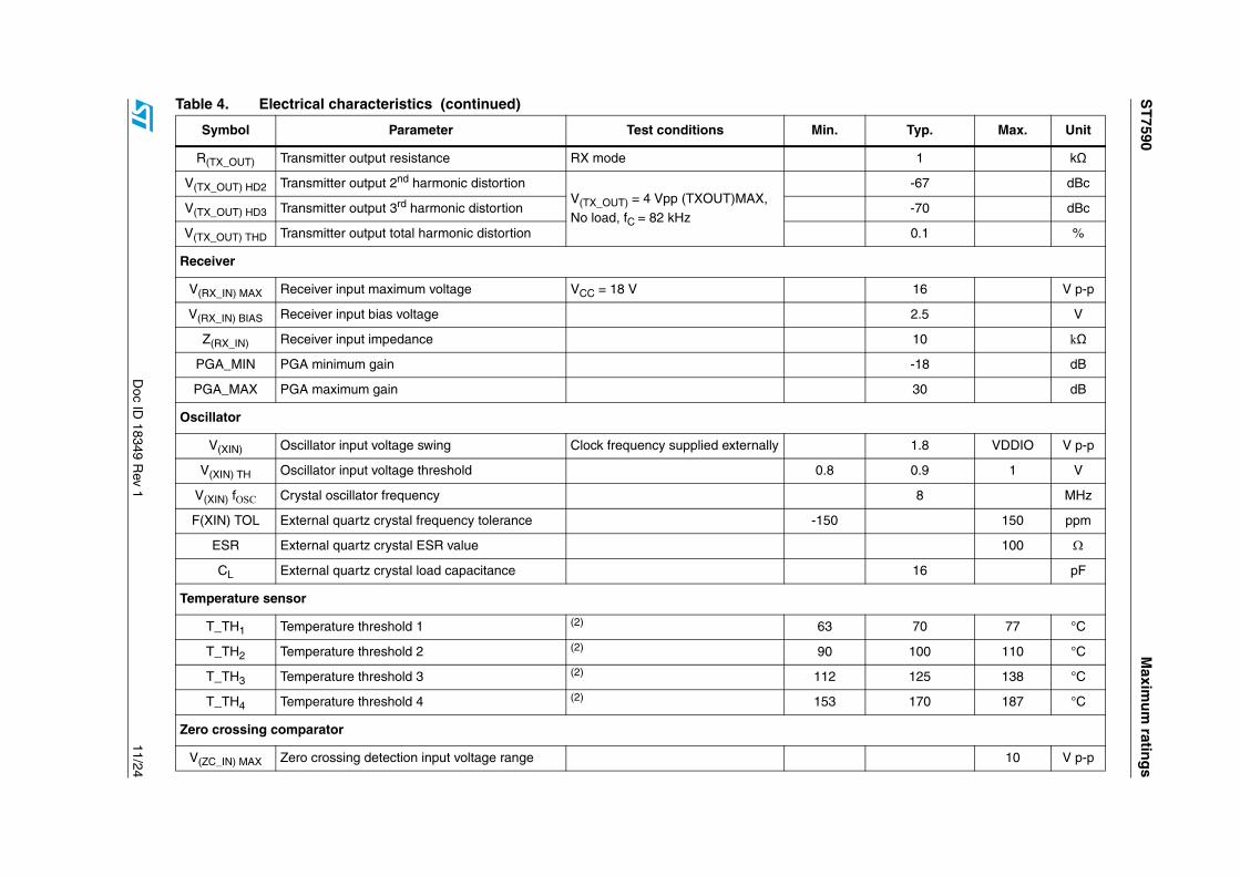
Table 4. Electrical characteristics (continued)
Symbol Parameter Test conditions Min. Typ. Max. Unit
ST
7590M
aximu
m ratin
gs
Doc ID
18349 Rev 1
11/24
R(TX_OUT) Transmitter output resistance RX mode 1 kΩ
V(TX_OUT) HD2 Transmitter output 2nd harmonic distortionV(TX_OUT) = 4 Vpp (TXOUT)MAX,
No load, fC = 82 kHz
-67 dBc
V(TX_OUT) HD3 Transmitter output 3rd harmonic distortion -70 dBc
V(TX_OUT) THD Transmitter output total harmonic distortion 0.1 %
Receiver
V(RX_IN) MAX Receiver input maximum voltage VCC = 18 V 16 V p-p
V(RX_IN) BIAS Receiver input bias voltage 2.5 V
Z(RX_IN) Receiver input impedance 10 kΩ
PGA_MIN PGA minimum gain -18 dB
PGA_MAX PGA maximum gain 30 dB
Oscillator
V(XIN) Oscillator input voltage swing Clock frequency supplied externally 1.8 VDDIO V p-p
V(XIN) TH Oscillator input voltage threshold 0.8 0.9 1 V
V(XIN) fOSC Crystal oscillator frequency 8 MHz
F(XIN) TOL External quartz crystal frequency tolerance -150 150 ppm
ESR External quartz crystal ESR value 100 Ω
CL External quartz crystal load capacitance 16 pF
Temperature sensor
T_TH1 Temperature threshold 1 (2) 63 70 77 °C
T_TH2 Temperature threshold 2 (2) 90 100 110 °C
T_TH3 Temperature threshold 3 (2) 112 125 138 °C
T_TH4 Temperature threshold 4 (2) 153 170 187 °C
Zero crossing comparator
V(ZC_IN) MAX Zero crossing detection input voltage range 10 V p-p
Table 4. Electrical characteristics (continued)
Symbol Parameter Test conditions Min. Typ. Max. Unit

Maxim
um
rating
sS
T7590
12/24D
oc ID 18349 R
ev 1
V(ZC_IN) TL Zero crossing detection input low threshold -44 -32 -17 mV
V(ZC_IN) TH Zero crossing detection input high threshold 26 41 56 mV
V(ZC_IN) HYST Zero crossing detection input hysteresis 73 mV
Digital section
Digital I/O
RPULL-UP Internal pull-up resistorsVDDIO = 3.3 V 66
kΩVDDIO = 5 V 41
VIH High logic level input voltage 0.65*VDDIO VDDIO+0.3 V
VIL Low logic level input voltage -0.3 0.35*VDDIO V
VOH High logic level output Voltage IOH= -4 mA VDDIO-0.4 V
VOL Low logic level output voltage IOL= 4 mA 0.4 V
UART interface
Data bits 8 Bits
Stop bits 1 Bits
Parity bits 0 Bits
Baud rate
-1.5% 57600 +1.5% BAUD
-1.5% 38400 +1.5% BAUD
-1.5% 19200 +1.5% BAUD
-1.5% 9600 +1.5% BAUD
Reset and power on
tRESETN Minimum valid reset pulse duration 1 µs
tSTARTUP Start-up time at power on or after a reset event (3) 35 60 ms
1. Referred to TA = -40°C
2. This parameter does not include the tolerance of external components
3. Referred to IC start up, uploading code from external NVM and its execution from external RAM may require some second.
Table 4. Electrical characteristics (continued)
Symbol Parameter Test conditions Min. Typ. Max. Unit

ST7590 Maximum ratings
Doc ID 18349 Rev 1 13/24
Figure 4. Power amplifier test circuit
C 1
10n
C 2
1u
R 3330k
R 4330k
R _LOAD50R
R 1
4k
R 2
15k
VC CVC C
S IGNA L S OURCE PA_IN_P
PA_IN_N
PA_OUT

Analog front end (AFE) ST7590
14/24 Doc ID 18349 Rev 1
4 Analog front end (AFE)
4.1 Reception pathFigure 5 shows the block diagram of the ST7590 input receiving path. The reception AFE main blocks are a wide input range analog PGA (programmable gain amplifier) and the ADC (analog to digital converter).
Figure 5. Reception path block diagram
The PGA is controlled by a loop algorithm that detects the amplifier output signal amplitude and adapts the gain of the amplifier in order to have the optimum input voltage range for the ADC. The PGA gain ranges from -18 dB up to 30 dB (typical), with steps of 6 dB (typical), as described in Table 5.
Table 5. PGA gain table
PGA code PGA gain (typical) RX_IN max range
[dB] [V p-p]
0 -18 16
1 -12 8
2 -6 4
3 0 2
4 6 1
5 12 0.500
6 18 0.250
7 24 0.125
8 30 0.0625

ST7590 Analog front end (AFE)
Doc ID 18349 Rev 1 15/24
4.2 Transmission pathFigure 6 shows the transmission path block diagram. It is mainly based on a digital to analog converter (DAC), capable to generate a very linear signal up to its full scale output. A gain control block before the DAC gives the possibility to scale down the output signal to match the desired transmission level.
Figure 6. Transmission path block diagram
According to PRIME Specifications the output level can be set on a 8-step logarithmic scale between a Maximum Output Level (MOL) and a minimum output level (MOL - 21dB), with steps of 3dB (typical). The maximum level corresponds to the TX_OUT full range.
4.3 Power amplifierThe integrated Power Amplifier is characterized by very high linearity, required to comply with the different international regulations (CENELEC, FCC etc.) limiting the spurious conducted emissions on the mains, and a current capability of 1Arms (typical) that allows the amplifier driving even very low impedance points of the network.
All pins of the Power Amplifier are accessible, making it possible to build an Active Filter network to increase the linearity of the output signal.
4.4 Thermal shutdown and temperature controlThe ST7590 performs an automatic shutdown of the power amplifier circuitry when the internal temperature exceeds 170 °C. After a Thermal shutdown event, the temperature must get below 125 °C before the ST7590 power amplifier comes back to operation.
Moreover a digital thermometer is embedded to identify the internal temperature among four zones, as indicated in Table 6.
Table 6. Temperature zones
Temperature zone Temperature range (Typ.)
1 T < T_TH1
2 T_TH1 < T < T_TH2
3 T_TH2 < T < T_TH3
4 T > T_TH3

Analog front end (AFE) ST7590
16/24 Doc ID 18349 Rev 1
4.5 Zero-crossing detectorThe ST7590 embeds an analog comparator with hysteresis, used for zero-crossing detection. Information about zero crossing events is managed as specified in PRIME protocol specifications.
4.6 One time programmable (OTP) memory arrayST7590 comes with an embedded 64 bit OTP array. This OTP memory is used to store hardware trimming values and the unique identifier EUI48, used for unique addressing in PRIME MAC protocol.
OTP array is composed of 4 16 bit words, indexed from 0 to 3, where the first (index 0) contains hardware trimming values, while the others contain the EUI48 address as specified in Table 7.
4.7 Power managementFigure 7 shows the power supply structure for the ST7590. The ST7590 operates from two external supply voltages:
VCC (8 to 18 V) as the main power supply;
VDDIO (3.3 or 5 V) for the I/O and digital sections.
Two internal linear regulators provide the remaining required voltages:
5 V regulator (used by the analog front end blocks), generated from the VCC voltage and connected to the VCCA pin;
1.8 V regulator (required for the DSP and microcontroller cores, the digital blocks, the PLL and the oscillator), generated from the VDDIO voltage and connected to the VDD_REG_1V8 pin.
All the supply voltages must be properly filtered, to their respective ground, using external capacitors close to each supply pin (see Figure 7).
Note: The internal regulators connected to VDD_REG_1V8 and VCCA are not designed to supply external circuitry; their output is externally accessible for filtering purpose only.
Table 7. OTP memory array
Index LSB MSB
0 Reserved – hardware trimming
1 EUI48[0..7] EUI48[8..15]
2 EUI48[16..23] EUI48[24..31]
3 EUI48[32..39] EUI48[40..47]

ST7590 Analog front end (AFE)
Doc ID 18349 Rev 1 17/24
Figure 7. Power supply internal scheme
4.8 Clock managementThe main clock source is an 8 MHz crystal connected to the internal oscillator through XIN and XOUT pins. Both XIN and XOUT pins have a 32 pF integrated capacitor, in order to drive a crystal having a load capacitance of 16 pF with no additional components.
Alternatively, an 8 MHz external clock can be directly supplied to XIN pin, leaving XOUT floating.
A PLL internally connected to the output of the oscillator generates the internal clocks needed by the digital part.
LDO
VCC
VSS
VCCA
VSSA
LDO
VDDIO
GND
VDD
VSSA
VDD_PLL
8-18VExternal Supply
3.3 or 5VExternal Supply
POWER AMPLIFIER
AFE
DIGITAL INTERFACES
DIGITAL CORE
INTERNAL PLL

Application information ST7590
18/24 Doc ID 18349 Rev 1
5 Application information
Figure 8. TQFP100 128 Kb external memory application example
Figure 9. QFN48 application example
EMCFilter
Switched ModePower Supply
Power LineInterface
Zero CrossingConditioning
Power AmplifierFeedback
HOSTController
SerialNon Volatile
Memory
ParallelAsynchronousRAM memory
ST7590
TQFP100
RXD
TXD
RESETn
GPIO6
SCLK1
MISO1
MOSI1
GPIO1
SRAM_A0..16
SRAM_D0..7
SRAM_OEN
SRAM_WEN
SRAM_CSN
VCC
VDDIO
PA_IN+
PA_IN-
TX_OUT
PA_OUT
RX_IN
ZC_IN
PHA
SE
NEU
TRAL
EMCFilter
Switched ModePower Supply
Power LineInterface
Zero CrossingConditioning
Power AmplifierFeedback
HOSTController
ST7590
QFN48
RXD
TXD
RESETn
GPIO6
VCC
VDDIO
PA_IN+
PA_IN-
TX_OUT
PA_OUT
RX_IN
ZC_IN
PHA
SE
NEU
TRAL

ST7590 Package mechanical data
Doc ID 18349 Rev 1 19/24
6 Package mechanical data
In order to meet environmental requirements, ST offers these devices in different grades of ECOPACK® packages, depending on their level of environmental compliance. ECOPACK® specifications, grade definitions and product status are available at: www.st.com. ECOPACK is an ST trademark.
Table 8. TQFP 100 package mechanical data
Dim. (mm)
Min. Typ. Max.
A 1.2
A1 0.05 0.15
A2 0.95 1 1.05
b 0.17 0.22 0.27
c 0.09 0.2
D 15.8 16 16.2
D1 13.8 14 14.2
D2 5.00 5.50
D3 12
E 15.8 16 16.2
E1 13.8 14 14.2
E2 5.00 5.50
E3 12
e 0.5
L 0.45 0.6 0.75
L1 1
k 0 3.5 7
ccc 0.08

Package mechanical data ST7590
20/24 Doc ID 18349 Rev 1
Figure 10. TQFP 100 package outline

ST7590 Package mechanical data
Doc ID 18349 Rev 1 21/24
Table 9. QFN-48 (7 x 7 mm) package mechanical data
Dim. (mm)
Min. Typ. Max.
A 0.80 0.90 1.00
A1 0.02 0.05
A2 0.65 1.00
A3 0.25
b 0.18 0.23 0.30
D 6.85 7.00 7.15
D2 4.95 5.10 5.25
E 6.85 7.00 7.15
E2 4.95 5.10 5.25
e 0.45 0.50 0.55
L 0.30 0.40 0.50
ddd 0.08

Package mechanical data ST7590
22/24 Doc ID 18349 Rev 1
Figure 11. QFN-48 (7 x 7 mm) package outline

ST7590 Revision history
Doc ID 18349 Rev 1 23/24
7 Revision history
Table 10. Document revision history
Date Revision Changes
19-Oct-2011 1 Initial release

ST7590
24/24 Doc ID 18349 Rev 1
Please Read Carefully:
Information in this document is provided solely in connection with ST products. STMicroelectronics NV and its subsidiaries (“ST”) reserve theright to make changes, corrections, modifications or improvements, to this document, and the products and services described herein at anytime, without notice.
All ST products are sold pursuant to ST’s terms and conditions of sale.
Purchasers are solely responsible for the choice, selection and use of the ST products and services described herein, and ST assumes noliability whatsoever relating to the choice, selection or use of the ST products and services described herein.
No license, express or implied, by estoppel or otherwise, to any intellectual property rights is granted under this document. If any part of thisdocument refers to any third party products or services it shall not be deemed a license grant by ST for the use of such third party productsor services, or any intellectual property contained therein or considered as a warranty covering the use in any manner whatsoever of suchthird party products or services or any intellectual property contained therein.
UNLESS OTHERWISE SET FORTH IN ST’S TERMS AND CONDITIONS OF SALE ST DISCLAIMS ANY EXPRESS OR IMPLIEDWARRANTY WITH RESPECT TO THE USE AND/OR SALE OF ST PRODUCTS INCLUDING WITHOUT LIMITATION IMPLIEDWARRANTIES OF MERCHANTABILITY, FITNESS FOR A PARTICULAR PURPOSE (AND THEIR EQUIVALENTS UNDER THE LAWSOF ANY JURISDICTION), OR INFRINGEMENT OF ANY PATENT, COPYRIGHT OR OTHER INTELLECTUAL PROPERTY RIGHT.
UNLESS EXPRESSLY APPROVED IN WRITING BY TWO AUTHORIZED ST REPRESENTATIVES, ST PRODUCTS ARE NOTRECOMMENDED, AUTHORIZED OR WARRANTED FOR USE IN MILITARY, AIR CRAFT, SPACE, LIFE SAVING, OR LIFE SUSTAININGAPPLICATIONS, NOR IN PRODUCTS OR SYSTEMS WHERE FAILURE OR MALFUNCTION MAY RESULT IN PERSONAL INJURY,DEATH, OR SEVERE PROPERTY OR ENVIRONMENTAL DAMAGE. ST PRODUCTS WHICH ARE NOT SPECIFIED AS "AUTOMOTIVEGRADE" MAY ONLY BE USED IN AUTOMOTIVE APPLICATIONS AT USER’S OWN RISK.
Resale of ST products with provisions different from the statements and/or technical features set forth in this document shall immediately voidany warranty granted by ST for the ST product or service described herein and shall not create or extend in any manner whatsoever, anyliability of ST.
ST and the ST logo are trademarks or registered trademarks of ST in various countries.
Information in this document supersedes and replaces all information previously supplied.
The ST logo is a registered trademark of STMicroelectronics. All other names are the property of their respective owners.
© 2011 STMicroelectronics - All rights reserved
STMicroelectronics group of companies
Australia - Belgium - Brazil - Canada - China - Czech Republic - Finland - France - Germany - Hong Kong - India - Israel - Italy - Japan - Malaysia - Malta - Morocco - Philippines - Singapore - Spain - Sweden - Switzerland - United Kingdom - United States of America
www.st.com