Embed Size (px)
Citation preview

Materials Sciences Division
Nanowire Solar Cells
Peidong YangDepartment of Chemistry
University of California, BerkeleyMaterials Science Division
Lawrence Berkeley National Laboratory

Materials Sciences Division MRS Bulletin, Jan 2005
Emerging PV
•• Low costLow cost•• Intermediate efficiencyIntermediate efficiency•• Environmental benignEnvironmental benign
•• Possible solar paintPossible solar paint

Materials Sciences Division
Emerging PV
Grätzel, M. Nature 414, 2001.
Alivisatos et al. Science 2002, 295, 2425.
Why nanowires are important?

Materials Sciences Division
PV Performance Metrics
Efficiency PP
FF V JP
out
in
oc sc
in
= =× ×
FF J VJ V
M M
SC OC
=

Materials Sciences Division
)1( dA e αη −−=
DLdED e /−=η
IQE(λ) = ηA(λ) ηED ηCT ηCC
ηPCE = =FF x VOC
PinPin
Pout ∫q F(λ)IQE(λ)dλ
S. Forrest. MRS Bulletin, Jan 2005

Materials Sciences Division
Emerging PV
Use of solar at terawatt levels requires drop in $/Wp
3N: New materials, New designs, New tricks
“dirty” semiconductorsorganicsoxides
absorbersbiological subunits
quantum effects
carrier multiplication
frequency shifting
Interface engineering
dye-sensitized cells
bulk heterojunction cells(polymer, organic-inorganic)

Materials Sciences Division
MLCT
Wavelength(nm)
Abs
orba
nce
Dye-sensitized Photoelectrochemical Cell
surface area of 800 – 1000 cm2 per cm2
η of 5 -10% with TiO2 nanoparticles
electron transport via trap-mediated diffusion
Low efficiency at long wavelength
Grätzel, M. Nature 414, 2001.
DSC characteristics
Poor charge collectors?
electron diffusivity: 10-4 cm2/s

Materials Sciences Division
1) Find dyes that function efficiently across the visible and near-IR
2) Raise open-circuit voltage closer to its theoretical maximum
3) Increase the electron diffusion length in the oxide anode, Ld = (Deτ)1/2
speed up electron transport slow recombination
engineer the active interface
random, polycrystalline network oriented single-crystalline channels
slow diffusive transport fast band conduction (field-assisted)
efficient for films ~10 μm thick in principle, efficient for much thicker cells
high internal surface area smaller internal surface area
adopt a nanowire geometry
Nanoparticle DSC Nanowire DSC
The three ways to improve DSC efficiency

Materials Sciences Division
Nanowire DSC: Design Principle
high nanowire densitylong, thin nanowires
electrode length (μm) diameter (nm) density (x1010 cm-2) SA
nanoparticle 8 - 10 15 - 30 n/a 800 - 1000
ideal nanowire 20 60 3 1080
achieved NW 20 130 0.3 ~200

Materials Sciences Division
Nanowire densities of 1-40 billion cm-2
Single-crystalline wires in direct contact with the substrateInexpensive and environmentally benignCompatible with arbitrary substrates of any size
Large-Scale Nanowire Array Synthesis
1st: dip-coat to get ZnO quantum dots 2nd: grow nanowires from QD seeds
zinc salthydrolysis,
HMTA
60-90 °C
L. Greene et al. Angew Chem. Int. Ed. 42, 3031, 2003.

Materials Sciences Division
H2N-(CH2CH2N)x-(CH2CH2NH)y-]-
CH2CH2NH2
Poly-ethylenimine (PEI):
Control of Nanowire Aspect Ratio
0 5 10 15 200
50
100
150
200
250
300
diam
eter
(nm
)
length (microns)
without PEI with PEI
DSCHybrid
Hybrid: aspect ratio = 10 DSC: aspect ratio > 150
5 μm500 nm

Materials Sciences Division
Alignment Control
500 nm
200 nm
Greene, L.E., Law, M. et al. Nano Letters 5, 1231 (2005).

Materials Sciences Division
360 370 380 390 400
I/a.u.
λ /nm
5 K 25 K 45 K 65 K 85 K 105 K 125 K 145 K 165 K 185 K 215 K 245 K 275 K 300 K 350 360 370 380 390 400 410
I/a.u.
λ/nm
300 400 500 600
λ / nm
E / a.u. A / a.u.
High Optical Quality
TEM shows that the nanowires are single crystals
Wire surfaces are clean (Raman, EELS) after 400 °C treatment

Materials Sciences Division
Characterization of Nanowire Arrays Electrical: Ohmic wire-substrate contacts FETs: Wires have high e- mobility
Individual wires are electrically conductive ρ = 0.1 - 1 Ω cm mobility: 1-5 cm2V-1s-1
electron diffusitivity: Dn=0.05-0.5 cm2s-1 [D = kBTμ/e ]Ensure larger electron diffusion length, avoiding possible
interfacial recombination
-1.0 -0.5 0.0 0.5 1.0
-1.5
-1.0
-0.5
0.0
0.5
1.0
1.5
-40 V-20 V0 V
20 V
40 V
I SD (μ
A)VSD (V)
-50 -25 0 25 500
255075
100125
VSD = 100 mV
I SD (n
A)
VG (V)
-1.0 -0.5 0.0 0.5 1.0
-1.5
-1.0
-0.5
0.0
0.5
1.0
1.5
-40 V-20 V0 V
20 V
40 V
I SD (μ
A)VSD (V)
-50 -25 0 25 500
255075
100125
VSD = 100 mV
I SD (n
A)
VG (V)
Law, M., Greene, L. et al. Nature Mater. 4, 455 (2005).

Materials Sciences Division
ηPCE = 1.5% under AM 1.5 G conditions
Nanowire based DSC
Black = 12 nm TiO2 NPBlue = 30 nm ZnO NPGreen = 200 nm ZnO NPRed = ZnO nanowires
• NW cells are competitive with thin TiO2nanoparticle cells (ηcc ~ 100%)• NW cells outperform ZnO nanoparticle cells
Law, M., Greene, L. et al. Nature Mater. 4, 455 (2005).
Materials Sciences Division
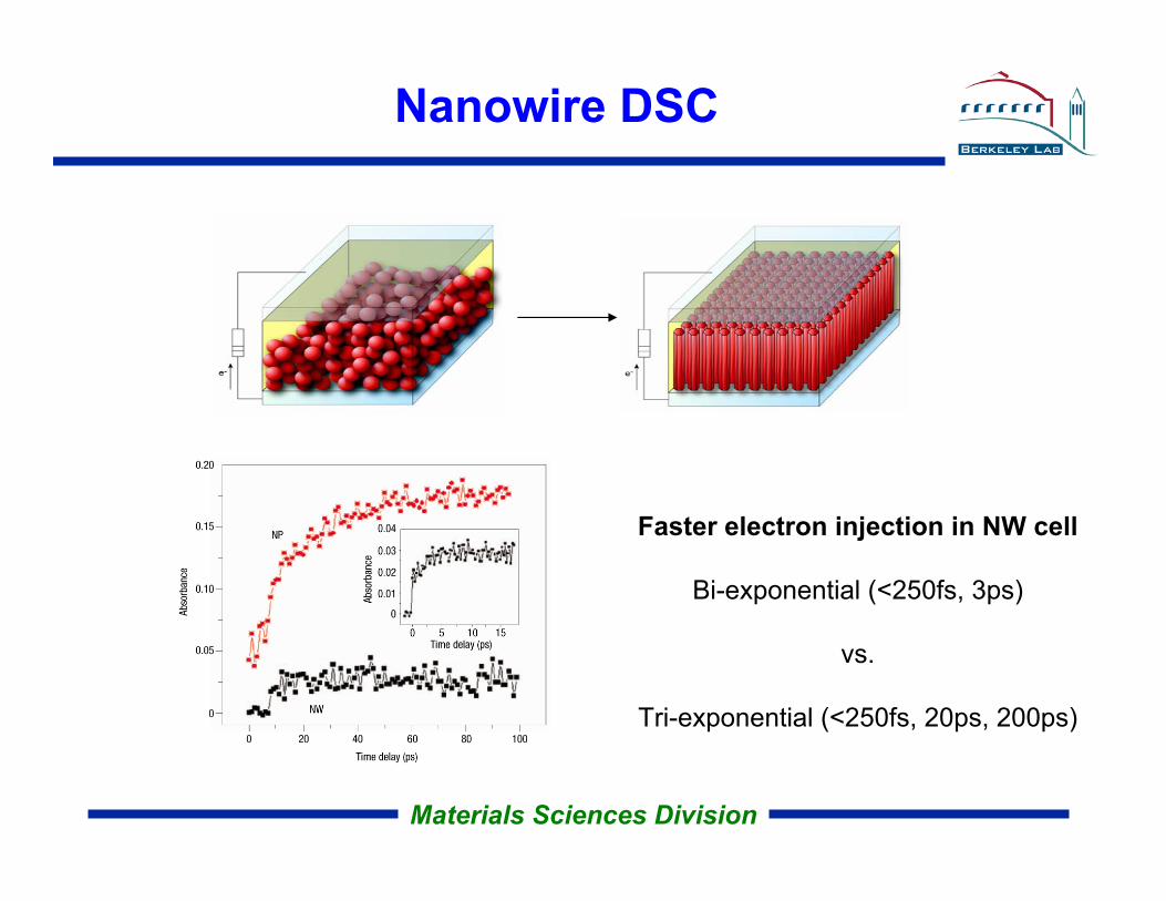
Nanowire DSC
Faster electron injection in NW cell
Bi-exponential (<250fs, 3ps)
vs.
Tri-exponential (<250fs, 20ps, 200ps)
Materials Sciences DivisionGrätzel, M, MRS Bulletin, Jan 2005
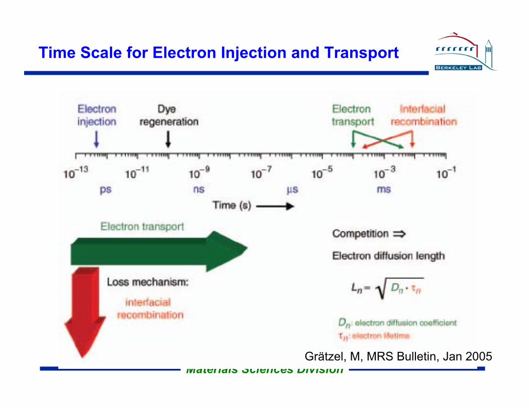
Time Scale for Electron Injection and Transport

Materials Sciences Division
Engineer active interface to reduce recombination
Core-sheath Nanowire Cells
Physically separate electrons and holes
Form a tunneling barrier
Passivate recombination centers on oxide surface
Overcoat the nanostructured electrode with an insulating or semiconducting oxide
Reduce recombination
Shift band edge to increase Voc
Use an oxide with a higher band edge energy
Form dipole layer that bends band upwards
Substrate
DyeRedox
Gregg, B. NREL.

Materials Sciences Division
Oxides: Al2O3, TiO2, Ta2O5, Nb2O5, ZrO2, HfO2, SnO2, ZnO, La2O3, Y2O3, CeO2, Sc2O3, Er2O3, V2O5, SiO2, In2O3, ...Perovskites: SrTiO3, BaTiO3, LiNbO3, LaMnO3 …Nitrides: AlN, TaNx, NbN, TiN, MoN, ZrN, HfN, GaN, ... Fluorides: CaF2, SrF2, ZnF2, ...Metals: Pt, Ru, Ir, Pd, Cu, Fe, Co, Ni, ... Carbides: TiC, NbC, TaC, ...Mixed structures: AlTiNx, AlTiOx, AlHfOx, SiO2:Al, HfSiOx, ... Sulfides: ZnS, SrS, CaS, PbS, ...Nanolaminates: HfO2/Ta2O5, TiO2/Ta2O5, TiO2/Al2O3, ZnS/Al2O3, ATO (AlTiO) ...Doping: ZnO:Al, ZnS:Mn, SrS:Ce, Al2O3:Er, ZrO2:Y, ... rare earth metals (Ce3+, Tb3+ etc.) also co-doping
Planar Systems, Inc.
Example: ZnS
Atomic Layer Deposition (ALD)

Materials Sciences Division
Core-sheath Nanowire Dye-sensitized Solar Cells

Materials Sciences Division
]-S
C6H13
-]
Poly(3-hexylthiophene)
1) ultrahigh nanowire density2) short, thin nanowires3) nanowires normal to substrate
2LD
Target nanowire array
2LD ~ 20 nm
S
S
S
S
S
CH3CH3 CH3
CH3 CH3
S
S
S
S
CH3 CH3
CH3 CH3
S
S
S
S
S
CH3CH3 CH3
CH3 CH3
S
S
S
S
CH3 CH3
CH3 CH3
S
S
S
S
S
CH3CH3 CH3
CH3 CH3
S
S
S
S
CH3 CH3
CH3 CH3
)-
)-
ca
0
-2.5
-3.5
-4.5
vacuum
ITOZnO
AgP3HT
~2.1 eV
Nanowire-polymer Hybrid Cell

Materials Sciences Division
Nanowire-polymer Composite Film
200 nm
Aligned wiresInter-wire spacing is 10-50 nm
2LD for P3HT ~ 20 nmThickness 200-300 nm

Materials Sciences Division
The Ideal Nanowire Cell
• Fully interdigitated donor-acceptor interface
• Acceptor wire array: high density, smaller band gap
• Donor: polymer/nanoparticles, maximize absorption
• Interface engineering: reduce recombination.
• Applicable to DSC, hybrid, and conventional semiconductor cells. N. Lewis
•• Low costLow cost•• Intermediate efficiencyIntermediate efficiency•• Environmental benignEnvironmental benign
•• Possible solar paintPossible solar paint

Materials Sciences Division
Dr. Matt Law
Lori Geene
Dwaud Tan
Funding
DOE
ITRI
AcknowledgementAcknowledgement