Embed Size (px)
Citation preview

Nanotechnology foundation & applications
By
Zainab saad hadi
History
• 1981– able to measure the size of an atom cluster on a
surface (IBM, Zurich)
• 1991– able to move atoms on surface (IBM, Almaden)
• 2002– able to assemble the molecules by physically
positioning the component atoms

Commercialization
• 1st generation (commercialized)– passive nanostructure
• applied in coatings, nanoparticles, bulk materials (nanostructured metals, polymers and ceramics)
– towards systematic design method
• 2nd generation– active nanostructure
• transistors, amplifier,targeted drugs and chemicals, and adaptive structures (~2005)
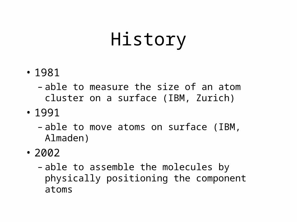
Commercialization
• 3rd generation– systems of nanosystems
• 3D features, heterogeneous nanocomponents• specific assembly techniques (such as bio-assembly,
networking at the nanoscale, new architectures)• ~2010
• 4th generation– molecular nanosystems
• nanodevices, biomimetics and new molecular designs (~2020)
Nanotechnology for the next generation
T.Nakahara & T. Imai
Sumitomo Electric Industries Ltd.
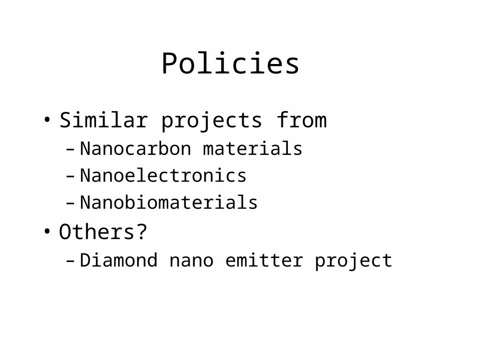
Policies
• Similar projects from– Nanocarbon materials– Nanoelectronics– Nanobiomaterials
• Others?– Diamond nano emitter project
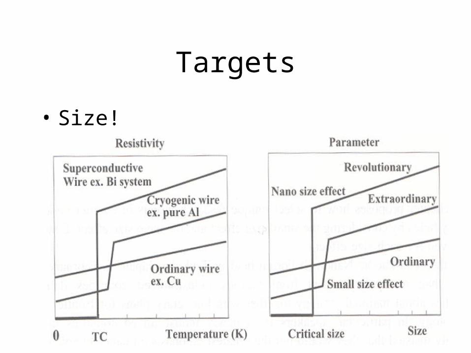
Targets
• Size!

Nano size effect
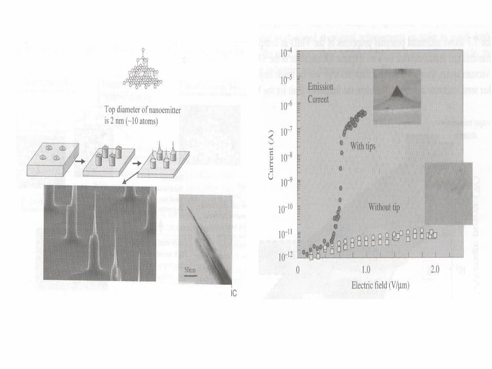
• Nanomaterial: diamond– rigid atomic structure
• high hardness, high thermal conductivity and high acoustic velocity
– semiconductor properties• apply as semiconductor devices, optical devices,
electron emission devices
– fabrication and synthesis technology• manufactured very precisely in a controlled manner

Applications
• Triode vacuum tube (~2000°C) VS. micro vacuum triode (~30°C)
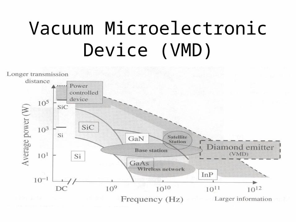
Vacuum Microelectronic Device (VMD)
Next generation applications for polymeric nanofibres
T.C. Lim and S.Ramakrishna
National University of Singapore

Polymeric fibres
• Targets– high tensile modulus and tensile strength– UV resistance, electrical conductivity,
biodegradability– typical: 1-100 m in diameter
• Nanofibres– decrease in pore size, a drop in structural
defects, enhanced physical behaviour
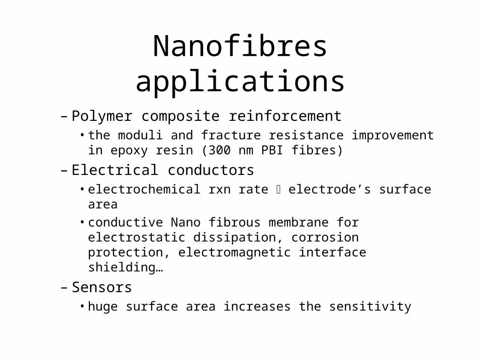
Nanofibres applications
– Polymer composite reinforcement• the moduli and fracture resistance improvement in
epoxy resin (300 nm PBI fibres)
– Electrical conductors• electrochemical rxn rate electrode’s surface area
• conductive Nano fibrous membrane for electrostatic dissipation, corrosion protection, electromagnetic interface shielding…
– Sensors• huge surface area increases the sensitivity