Embed Size (px)
Citation preview

NanotechnologNanotechnologyy Dr.S.Sanyasi RajuDr.S.Sanyasi Raju
Reader in PhysicsReader in Physics M.R.College(Autonomus)M.R.College(Autonomus) VIZIANAGARAMVIZIANAGARAM

Nanotechnology refers broadly to a field of applied science and technology whose
unifying theme is the control of matter on
the molecular level in scales smaller
than 1 micrometre, normally 1 to 100 nanometers, and the fabrication of devices within that size
range.

The term nano comes from a Greek The term nano comes from a Greek word meaning dwarf.word meaning dwarf.
Nanotechnology is science and Nanotechnology is science and engineering at the scale of atoms engineering at the scale of atoms and moleculesand molecules
Materials at the nanoscale are Materials at the nanoscale are typically between 0.1 and 100 typically between 0.1 and 100 nanometres (nm) in size nanometres (nm) in size
1 nm is one billionth of a metre (10-9 1 nm is one billionth of a metre (10-9 m).m).

Most atoms are 0.1 to 0.2 nm wideMost atoms are 0.1 to 0.2 nm wide
Strands of DNA are around 2 nm wide, Strands of DNA are around 2 nm wide,
Red blood cells are around 7000 nm in Red blood cells are around 7000 nm in diameterdiameter
Human hairs are typically 80,000 nm Human hairs are typically 80,000 nm across.across.
A nanometre is also about the length A nanometre is also about the length human fingernails grow by each second.human fingernails grow by each second.

Materials of this size can display strikingly Materials of this size can display strikingly different physical and chemical properties, different physical and chemical properties, compared with larger particles of the same compared with larger particles of the same material.material.
These properties are largely due to two factorsThese properties are largely due to two factors
Smaller particles have a relatively larger Smaller particles have a relatively larger surface area, compared with their volume, surface area, compared with their volume, making them much more chemically reactivemaking them much more chemically reactive
In addition - at scales below 100 nm - the In addition - at scales below 100 nm - the weird quantum effects of the atomic world weird quantum effects of the atomic world start to take hold. start to take hold.
Quantum effects can change the optical, Quantum effects can change the optical, electronic or magnetic qualities of materials in electronic or magnetic qualities of materials in unpredictable ways.unpredictable ways.

Materials reduced to the nanoscale can suddenly show very different properties compared to what they exhibit on a macroscale, enabling unique applications.
For instance, opaque substances become transparent (copper); inert materials become catalysts (platinum);
Stable materials turn combustible (aluminum); solids turn into liquids at room temperature (gold);
Insulators become conductors (silicon).
A material such as gold, which is chemically inert at normal scales, serve as a potent chemical catalyst at nanoscales
Much of the fascination with nanotechnology stems from these unique quantum and surface phenomena that matter exhibits at the nanoscale.
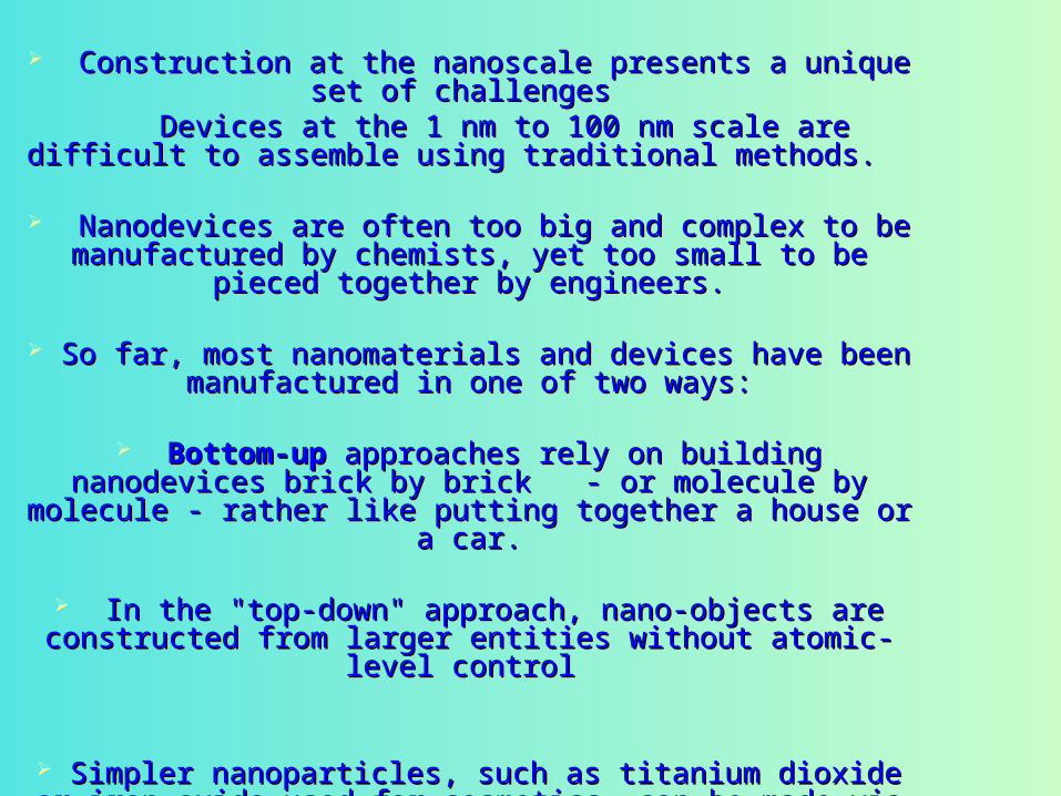
Construction at the nanoscale presents a unique set of Construction at the nanoscale presents a unique set of challengeschallenges
Devices at the 1 nm to 100 nm scale are difficult to Devices at the 1 nm to 100 nm scale are difficult to assemble using traditional methods.assemble using traditional methods.
Nanodevices are often too big and complex to be Nanodevices are often too big and complex to be manufactured by chemists, yet too small to be pieced manufactured by chemists, yet too small to be pieced
together by engineers.together by engineers.
So far, most nanomaterials and devices have been So far, most nanomaterials and devices have been manufactured in one of two ways:manufactured in one of two ways:
Bottom-upBottom-up approaches rely on building nanodevices brick approaches rely on building nanodevices brick by brick - or molecule by molecule - rather like putting by brick - or molecule by molecule - rather like putting
together a house or a car.together a house or a car.
In the "top-down" approach, nano-objects are constructed In the "top-down" approach, nano-objects are constructed from larger entities without atomic-level controlfrom larger entities without atomic-level control
Simpler nanoparticles, such as titanium dioxide or iron Simpler nanoparticles, such as titanium dioxide or iron oxide used for cosmetics, can be made via chemical oxide used for cosmetics, can be made via chemical
synthesis.synthesis.

Nanotechnology in consumer devices Nanotechnology in consumer devices and other applications right nowand other applications right now : :
Computer hard drivesComputer hard drives Car parts and catalytic converters Car parts and catalytic converters Scratch- and wear-resistant paints and Scratch- and wear-resistant paints and
coatingscoatings Sunscreens (titanium dioxide nanoparticles Sunscreens (titanium dioxide nanoparticles
are transparent, yet absorb UV light at the are transparent, yet absorb UV light at the same time) same time)
Metal cutting toolsMetal cutting tools Antibacterial bandages incorporating silver Antibacterial bandages incorporating silver
nanoparticlesnanoparticles Nanofilm-coated "self-cleaning" windows andNanofilm-coated "self-cleaning" windows and Stain-resistant fabricsStain-resistant fabrics

Atom-thick carbon transistor could succeed silicon Graphene makes graphite when stacked in layers, and carbon nanotubes when rolled into a tube.

Size matters when it comes to graphene circuits
When it comes to using nanoscopic ribbons of graphene to make electronic circuits, researchers have discovered that size really does matter.
Supercomputer simulations of quantum mechanical behaviour suggest that not just the width, but also the length, of these atom-thin sheets of carbon determines whether they will act as a conductor or a semiconductor A finding that could prove helpful for harnessing graphene's unique electronic properties. Nanoribbons are long, thin strips of graphene that are etched from graphene sheets using electron-beam lithography.

Because graphene can be either a conductor or semiconductor, and because it can transport electrons long distances with little scattering, it could be an ideal material for nanoelectronic devices.
Some researchers think that they might be able to make entire integrated circuits using only components made out of graphene.
Graphene was first produced in the lab in 2004 by repeatedly peeling off successive layers off of graphite – a process known as "mechanical exfoliation".

Graphene also conducts electricity faster than most materials since electrons can travel through in straight lines between atoms without being scattered.
This could ultimately mean faster, more efficient electronic components that also require less power.

Buckminsterfullerene C60, also known as the buckyball,
is the simplest of the carbon structurescarbon structures known as fullerenes. Members of the fullerene family are a major subject of research falling under the nanotechnology umbrella.

Image of reconstructionreconstruction on a clean Au (100)Au (100) surface, as visualized using scanning tunnelingscanning tunneling microscopymicroscopy. The individual atomsatoms composing the surface are visible.

The World's Smallest CarThe World's Smallest Car

THIS YEAR NOBLE PRIZE INTHIS YEAR NOBLE PRIZE IN
PHYSICS WAS AWARDED TOPHYSICS WAS AWARDED TOALBERT FERT OF FRANCE AND ALBERT FERT OF FRANCE AND
PETER GRINBERG OF GERMANY PETER GRINBERG OF GERMANY
FOR THEIR PIONEERING WORK ON FOR THEIR PIONEERING WORK ON
GIANT MAGNETO RESISTENCE GIANT MAGNETO RESISTENCE (GMR)(GMR)

THIS NANOTECHNOLOGY MINIATURISED THIS NANOTECHNOLOGY MINIATURISED
THE HEAD THAT READS THE THE HEAD THAT READS THE
HARD DISK THAT STORESHARD DISK THAT STORES
GIGA BYTES GIGA BYTES OF INFORMATION, OF INFORMATION,
BE IT BE IT
SCIENTIFIC DATA OR MUSIC, IN A JIFFY.SCIENTIFIC DATA OR MUSIC, IN A JIFFY.

MAGNETORESISTANCE (MR) IS CHANGE IN THE MAGNETORESISTANCE (MR) IS CHANGE IN THE
RESISTANCE TO FLOW OFRESISTANCE TO FLOW OF
CURRENT IN A CONDUCTOR, WHEN PLACED IN A CURRENT IN A CONDUCTOR, WHEN PLACED IN A
MAGNETIC FIELDMAGNETIC FIELD
THE CONDUCTOR IN THIS CASE MUST BE A MAGNETTHE CONDUCTOR IN THIS CASE MUST BE A MAGNETLIKE Fe, Co, OR NiLIKE Fe, Co, OR Ni
AN INCREASE IN RESISTANCE WAS NOTICED WHEN AN INCREASE IN RESISTANCE WAS NOTICED WHEN
THE CONDUCTING OF ELECTRIC CURREENT WAS THE CONDUCTING OF ELECTRIC CURREENT WAS
PARALLAL TO THE MAGNETIC FIELDPARALLAL TO THE MAGNETIC FIELD
RESISTANCE DECREASES WHEN THE MAGNETIC RESISTANCE DECREASES WHEN THE MAGNETIC
FIELD IS APPLIED IN TRANSVERSE DIRECTIONFIELD IS APPLIED IN TRANSVERSE DIRECTIONBUT THIS CHANGE IS MINIMALBUT THIS CHANGE IS MINIMAL

IN GMR METHOD, FERT AND GRUNBERG SANDWITCHRDIN GMR METHOD, FERT AND GRUNBERG SANDWITCHRD
A LAYER OF NON MAGNETIC METAL CrA LAYER OF NON MAGNETIC METAL Cr
BETWEEN THE TWO LAYERS OF MAGNETIC METAL IRONBETWEEN THE TWO LAYERS OF MAGNETIC METAL IRON
THESE LAYERS ARE A FEW NANOMETERS THICK ONLYTHESE LAYERS ARE A FEW NANOMETERS THICK ONLY
The TECHNIQUQ USED IS MOLECULAR BEAM EPITAXY (IN EARLY 70S)The TECHNIQUQ USED IS MOLECULAR BEAM EPITAXY (IN EARLY 70S)
LATER TECHNIQUES USED ARE SPUTTERING , LASER ABLATION AND LATER TECHNIQUES USED ARE SPUTTERING , LASER ABLATION AND
CHEMICALCHEMICAL VAPOUR DEPOSITIONVAPOUR DEPOSITION

THE TWO MAGNETIC LAYERS ARE MAGNETISED IN THE THE TWO MAGNETIC LAYERS ARE MAGNETISED IN THE
SAME DIRECTION IN ONE CASE AND IN OPPOSITE DIRECTIONSAME DIRECTION IN ONE CASE AND IN OPPOSITE DIRECTION
IN ANOTHER CASEIN ANOTHER CASE THE RESISTANCE TO FLOW OF ELECTRONS THE RESISTANCE TO FLOW OF ELECTRONS
THROUGH THE SANDWITCH WAS MUCH HIGHER IN THE SECOND THROUGH THE SANDWITCH WAS MUCH HIGHER IN THE SECOND
CASE THA N IN THE FIRSTCASE THA N IN THE FIRST
THIS IS DUE TO ELECTRONS HAVING ANTI PARALLAL SPINSTHIS IS DUE TO ELECTRONS HAVING ANTI PARALLAL SPINS
THIS DIFFERENTIAL FLOW OF CURREENT DUE TO OPPOSITE THIS DIFFERENTIAL FLOW OF CURREENT DUE TO OPPOSITE
MAGNETIC FIELDS IS CALLED GMRMAGNETIC FIELDS IS CALLED GMR

Grunsberg obtained a change of resistance of 10% WITH Grunsberg obtained a change of resistance of 10% WITH THREE LAYERSTHREE LAYERSFERT CREATED A SANDWITCH OF30 LAYERS OF Fe AND FERT CREATED A SANDWITCH OF30 LAYERS OF Fe AND OBSERVED A 50% CHANGE IN RESISTANCEOBSERVED A 50% CHANGE IN RESISTANCE
IRON AND CHROMIUM HAVE MATCHING LATTICE PARAMETERS-fcc IRON AND CHROMIUM HAVE MATCHING LATTICE PARAMETERS-fcc STRUCTURESTRUCTURE
Latest Co-Ge LAYERS ARE USED FOR TUNNELING Latest Co-Ge LAYERS ARE USED FOR TUNNELING MAGNETORESISTANCE MAGNETORESISTANCE ( TMR )( TMR )
TMR TECHNOLGY IS ALREADY IN USE IN MAGNETIC ACCESS TMR TECHNOLGY IS ALREADY IN USE IN MAGNETIC ACCESS MEMORIES MEMORIES ( MRAM ) FOR LAPTOPS( MRAM ) FOR LAPTOPS
SOON TMR WILL REPLACE GMRSOON TMR WILL REPLACE GMR
ALSO THE DISCOVERY OF GMR HAS OPENED A NEW FIELD OF ALSO THE DISCOVERY OF GMR HAS OPENED A NEW FIELD OF SCIENCE SCIENCE CALLAD MAGNETOELECTRONICS OS SPINTRONICSCALLAD MAGNETOELECTRONICS OS SPINTRONICS


So what are the real risks - does nanotechnology pose a threat to human health or the environment? Nanoparticles such as buckyballs and carb nanotubes are already with us - and one concern is that they might present different dangers to bulk versions of the same materials. Some environmental groups are worried that these materials are now going into our bodies and the environment with little knowledge about their long-term effects.
Some groups have called for a moratorium on research until we know more.
While these nanoparticles might present a risk, we just do not know if we would ever be exposed to enough of them to cause harm

Aside from the health risks, some commentators have expressed concern about the potential ethical and social effects the wider use of nanotechnologies might have on society.
For example nanotech could change the fundamental nature of what it means to be human. We may develop technologies to prolong our life, improve endurance or even make us a little bit smarter.