Embed Size (px)
Citation preview

Nanoscale
PAPER
Publ
ishe
d on
11
Apr
il 20
14. D
ownl
oade
d by
Duk
e U
nive
rsity
on
12/0
5/20
14 1
6:24
:25.
View Article OnlineView Journal
aDepartment of Chemistry, Duke University,
North Carolina 27708, USA. E-mail: benjambDepartment of Chemistry, University of No
North Carolina 27599, USAcCurriculum in Applied Sciences and Engin
Chapel Hill, Chapel Hill, North Carolina 27
† Electronic supplementary informa10.1039/c4nr01024h
‡ These authors contributed equally to th
Cite this: DOI: 10.1039/c4nr01024h
Received 24th February 2014Accepted 10th April 2014
DOI: 10.1039/c4nr01024h
www.rsc.org/nanoscale
This journal is © The Royal Society of
Solution-processed copper–nickel nanowireanodes for organic solar cells†
Ian E. Stewart,‡a Aaron R. Rathmell,‡a Liang Yan,b Shengrong Ye,a Patrick F. Flowers,a
Wei Youbc and Benjamin J. Wiley*a
This work describes a process to make anodes for organic solar cells from copper–nickel nanowires with
solution-phase processing. Copper nanowire films were coated from solution onto glass and made
conductive by dipping them in acetic acid. Acetic acid removes the passivating oxide from the surface of
copper nanowires, thereby reducing the contact resistance between nanowires to nearly the same
extent as hydrogen annealing. Films of copper nanowires were made as oxidation resistant as silver
nanowires under dry and humid conditions by dipping them in an electroless nickel plating solution.
Organic solar cells utilizing these completely solution-processed copper–nickel nanowire films exhibited
efficiencies of 4.9%.
1. Introduction
It's been noted that a solar energy conversion system cannotcost much more than �10 times the cost of paint, or �$10 perm2, if it is to be cost-competitive with fossil fuels.1,2 However,indium tin oxide (ITO), the transparent conductor used forsolution-coatable organic photovoltaics (OPVs), by itself costsbetween $20–$90 per m2.3 Making the cost of OPVs competitivewith fossil fuels will require transparent conductive paint thatcosts �10 times less than ITO.
The high cost of ITO arises from several factors. Indium is afairly rare and expensive (�$600 per kg) element, with anabundance in the earth's crust close to that of Ag (0.05 ppm).4,5
ITO lm is manufactured with a sputtering process that is fairlyslow; the fastest lm throughputs are around 0.01 m s�1. Inaddition, less than 30% of the ITO sputtered from a target isdeposited on the substrate, requiring a recycling infrastructurethat adds additional cost.4
The high cost of ITO has driven a search for solution-coat-able alternatives that can enable lm throughputs up to 1000times faster than ITO sputtering, near-complete transfer of thedeposited material to the lm, and comparable performance.Solution-coatable alternatives that have received extensiveattention include conductive polymers,6,7 carbon nanotubes,8–10
124 Science Drive, Box 90354, Durham,
rth Carolina at Chapel Hill, Chapel Hill,
eering, University of North Carolina at
599, USA
tion (ESI) available. See DOI:
is work.
Chemistry 2014
graphene,9,11 and metal nanowires.12–16 Of these solution-coat-able alternatives, only silver nanowires (Ag NWs) have demon-strated performance that exceeds that of ITO. As the coatingprocess for Ag NWs is less costly and orders of magnitude fasterthan for ITO, Ag NWs will likely replace ITO as the transparentconductor of choice for applications that require relativelythick, high-conductivity (i.e., high-cost) ITO, such as touchscreens, organic light emitting diodes (OLEDs), andOPVs.3,12,17,18 However, the price and abundance of Ag is similarto that of In.4,5
Copper is 6% less conductive than silver, but it is 1000 timesmore abundant and 100 times less expensive.5,19 Thus, replacingAg NWs with copper nanowires (Cu NWs) should offer compa-rable levels of performance at lower cost. One disadvantage ofCu NWs relative to Ag NWs is that they have a greater potentialto oxidize, which reduces the conductivity of the lm. Althoughlms of Ag NWs can be heated in air to sinter them together atthe contacts, and thereby reduce the contact resistance betweennanowires, the fact that Cu NWs are covered with a layer ofcopper oxide prevents them from sintering together in air.Instead, it has been necessary to anneal Cu NW lms underhydrogen in order for the lms to obtain performance compa-rable to that of Ag NWs.15,20–22 Despite the lower cost of Cu NWs,this lack of stability and necessity of hydrogen annealing hashindered their wider use in practical applications.
The challenges associated with making Cu NW networksconductive and protecting them from oxidation are likelyresponsible for the fact that there are many articles exploringthe use of Ag NWs as a replacement for ITO in solar cells,12,13,23–26
but only one recent report on the use of solution-coated Cu NWsin an OPV.27 In that work, following hydrogen annealing of theCu NW lm, the nanowire electrode was planarized withPEDOT:PSS. The authors noted that the processing conditions
Nanoscale

Nanoscale Paper
Publ
ishe
d on
11
Apr
il 20
14. D
ownl
oade
d by
Duk
e U
nive
rsity
on
12/0
5/20
14 1
6:24
:25.
View Article Online
had to be modied to prevent the degradation of the Cu NWlm during coating of the acidic PEDOT:PSS suspension. Theauthors vacuum deposited the remaining layers onto this anodeto create a bulk-heterojunction (BHJ) small-molecule organicsolar cell with an efficiency of 3%. Although this work demon-strated that Cu NWs can be used as an anode in a solar cell,unprotected Cu NWs are clearly not well-suited for this purposesince they will gradually become non-conductive due to oxida-tion over a matter of months.28
In this work we demonstrate an all solution-phase process tocoat Cu NWs to form a lm, make this lm conductive, andprotect it against oxidation. Aer coating Cu NWs from an inkonto glass, the lms were made conductive by simply dippingthem in acetic acid. These lms were thenmade relatively stableagainst further oxidation by dipping them in a Ni electrolessplating solution. Copper–nickel nanowire (CuNi NW) lms werethen integrated into a solution-coated OPV to give a deviceefficiency of 4.9%.
2. Experimental2.1. Materials and instrumentation
For all nanowire lms, transmittance and absorption data werecollected using a UV-vis-NIR spectrophotometer (Cary 6000i)and sheet resistance values were measured using a four-pointprobe (Signatone SP4-50045TBS). The data points in Fig. 1D, 2Dand 4A are each an average of 5 probe measurements. Metalconcentration measurements were completed using a PerkinElmer 3100 atomic absorption spectrophotometer (AAS).Pressing was performed with a shop press (model H6233Z) fromGrizzly Industrial. Plasma cleaning was performed with a Har-rick Plasma PDC-001. Optical microscopy images were takenwith an Olympus BX51 microscope. SEM (FEI XL30 SEM-FEG),TEM (FEI Tecnai G2 Twin), and AFM (Digital InstrumentsDimension 3100) images were taken at the Shared MaterialsInstrumentation Facility at Duke University. Humidity chambermeasurements were made in a Test Equity 200H Seriestemperature/humidity chamber at 85 �C/85 RH. Photovoltaicperformance was characterized with a solar simulator (Oriel91160, 300 W) under AM1.5 global one sun (100 mW cm�2
calibrated by a NREL certied standard silicon cell) at roomtemperature in a glove box. Current density vs. potential (J–V)curves were recorded with a Keithley 2400 digital source meter.The incident photon-to-current conversion efficiency (IPCE)measurements were carried out under monochromatic illumi-nation (Oriel Cornerstone 260 1/4 m monochromator equippedwith an Oriel 70613NS QTH lamp), and the calibration of theincident light was performed with a monocrystalline silicondiode.
2.2. Preparation of nanowire lms
Copper nanowires (L ¼ 20 � 5 mm, D ¼ 67 � 15 nm) weresynthesized by previously reported methods and donated byNanoForge Corp.20 To separate the nanowires (1.4 mg mL�1
copper) from their storage solution of polyvinylpyrrolidone(PVP, 1 wt% in DI water, Aldrich) and diethylhydroxylamine
Nanoscale
(DEHA, 1 wt% in DI water, Aldrich), several purication stepswere required. First, an aliquot (1 mL) of nanowires wascollected and centrifuged at 2000 rpm for 5 minutes followed bydecantation of the PVP–DEHA supernatant. The nanowireaggregates were then washed three times with DEHA (1 mL, 3 wt% in DI water) to remove the remaining PVP. Next, the nano-wires were washed with 190 proof ethanol (1 mL, Koptec) toextract any residual water. The nanowires were then washedwith an ink formulation consisting of 0.06 g nitrocellulose(Scientic Polymer) dissolved in 2.94 g acetone (EMD) withsubsequent addition of 3 g ethanol (Pharmaco-Aaper), 0.5 gethyl acetate (Aldrich), 1 g pentyl acetate (Aldrich), 1 g iso-propanol (BDH), and 1.7 g toluene (Aldrich). The suspensionwas briey vortexed and sonicated (<5 seconds) betweenwashing steps.
Prior to preparing the Cu NW transparent electrodes, theglass substrates (3 in � 1 in microscope slides, VWR) weresonicated in acetone for ten minutes and transferred to iso-propanol to remove surface contaminants. The slides werewiped dry with a kimwipe and blown dry under air immediatelyprior to nanowire deposition. Following decantation of the inkwash supernatant, a small amount (0.3 mL) of the ink wasadded to the nanowires resulting in a nal Cu NW concentra-tion of�4.5 mgmL�1. This suspension was vortexed to dispersethe nanowires in the ink, and 35 mL was pipetted in a line acrossthe top of the glass slide. A Meyer rod (Gardco #13) was thenquickly (<1 second) drawn down the slide by hand to evenlyspread the nanowire coating. The amount of ink added to thenanowires can be adjusted to vary the Cu NW concentration,and thus the transmittance and conductivity of the resultinglm.
The slides coated with CuNWswere dried in air for 10minutesat 80 �C. Once the slides returned to room temperature, they weredipped in glacial acetic acid (Aldrich) for 2 seconds (Fig. 1A), driedunder N2 gas, and placed in an 80 �C oven for 45 seconds.Following four cycles of this procedure, the slides were allowed tocool to room temperature and then dipped in acetic acid anddried under N2 twice more without additional oven drying. Insome cases the slides were pressed at 80 bar at room temperaturefor one minute between glass slides functionalized with1H,1H,2H,2H-peruorooctyltriethoxysilane (Aldrich). To performthis functionalization, the slides were rst plasma cleaned in airat a pressure of 0.8 to 0.93 mbar for 1 minute and placed in adessicator under vacuum overnight along with an open vial con-taining 1 drop of 1H,1H,2H,2H-peruorooctyltriethoxysilane.
For the Cu NW lms annealed under H2, the lms werecoated from the ink and dried in the oven as above. Instead ofan acetic acid dip, the lms were plasma cleaned under forminggas (95% N2, 5% H2) for 10 minutes at a pressure of 600 to 700mTorr to remove residual organic material from the electrodes.Next, the electrodes were heated to 175 �C in a tube furnaceunder constant H2 ow (600 mL min�1) for 30 minutes toeliminate the remaining nitrocellulose and anneal the nano-wires together.20
Silver nanowires were synthesized following previouslypublished methods to give nanowires with dimensions of L ¼15 � 3 mm and D ¼ 63 � 7 nm.29,30 Electrodes of Ag NWs were
This journal is © The Royal Society of Chemistry 2014

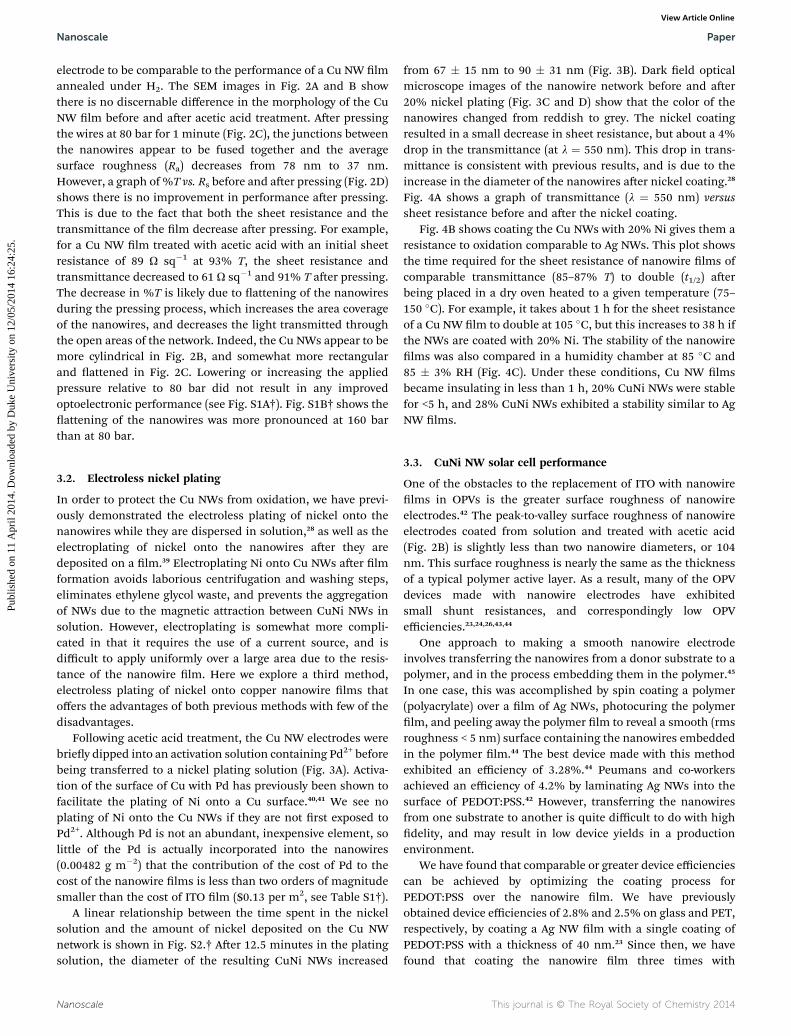
Fig. 1 (A) Cu NW film coated on a glass slide immersed in glacial acetic acid. TEM images of the same Cu NW (B) before and (C) after acetic acidtreatment. (D) Plot of transmittance vs. sheet resistance for Cu NW films after annealing under H2 at 175 �C or after the acetic acid treatment.
Fig. 2 SEM images of Cu NWs (A) as deposited, (B) washed with acetic acid, and (C) after pressing at 80 bar. (D) Plot of transmittance vs. sheetresistance of acetic acid washed Cu NW films before and after pressing.
This journal is © The Royal Society of Chemistry 2014 Nanoscale
Paper Nanoscale
Publ
ishe
d on
11
Apr
il 20
14. D
ownl
oade
d by
Duk
e U
nive
rsity
on
12/0
5/20
14 1
6:24
:25.
View Article Online
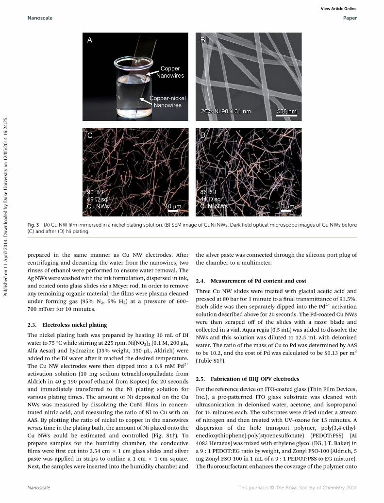
Fig. 3 (A) Cu NW film immersed in a nickel plating solution. (B) SEM image of CuNi NWs. Dark field optical microscope images of Cu NWs before(C) and after (D) Ni plating.
Nanoscale Paper
Publ
ishe
d on
11
Apr
il 20
14. D
ownl
oade
d by
Duk
e U
nive
rsity
on
12/0
5/20
14 1
6:24
:25.
View Article Online
prepared in the same manner as Cu NW electrodes. Aercentrifuging and decanting the water from the nanowires, tworinses of ethanol were performed to ensure water removal. TheAg NWs were washed with the ink formulation, dispersed in ink,and coated onto glass slides via a Meyer rod. In order to removeany remaining organic material, the lms were plasma cleanedunder forming gas (95% N2, 5% H2) at a pressure of 600–700 mTorr for 10 minutes.
2.3. Electroless nickel plating
The nickel plating bath was prepared by heating 30 mL of DIwater to 75 �C while stirring at 225 rpm. Ni(NO3)2 (0.1 M, 200 mL,Alfa Aesar) and hydrazine (35% weight, 150 mL, Aldrich) wereadded to the DI water aer it reached the desired temperature.The Cu NW electrodes were then dipped into a 0.8 mM Pd2+
activation solution (10 mg sodium tetrachloropalladate fromAldrich in 40 g 190 proof ethanol from Koptec) for 20 secondsand immediately transferred to the Ni plating solution forvarious plating times. The amount of Ni deposited on the CuNWs was measured by dissolving the CuNi lms in concen-trated nitric acid, and measuring the ratio of Ni to Cu with anAAS. By plotting the ratio of nickel to copper in the nanowiresversus time in the plating bath, the amount of Ni plated onto theCu NWs could be estimated and controlled (Fig. S1†). Toprepare samples for the humidity chamber, the conductivelms were rst cut into 2.54 cm � 1 cm glass slides and silverpaste was applied in strips to outline a 1 cm � 1 cm square.Next, the samples were inserted into the humidity chamber and
Nanoscale
the silver paste was connected through the silicone port plug ofthe chamber to a multimeter.
2.4. Measurement of Pd content and cost
Three Cu NW slides were treated with glacial acetic acid andpressed at 80 bar for 1 minute to a nal transmittance of 91.5%.Each slide was then separately dipped into the Pd2+ activationsolution described above for 20 seconds. The Pd-coated Cu NWswere then scraped off of the slides with a razor blade andcollected in a vial. Aqua regia (0.5 mL) was added to dissolve theNWs and this solution was diluted to 12.5 mL with deionizedwater. The ratio of the mass of Cu to Pd was determined by AASto be 10.2, and the cost of Pd was calculated to be $0.13 per m2
(Table S1†).
2.5. Fabrication of BHJ OPV electrodes
For the reference device on ITO-coated glass (Thin Film Devices,Inc.), a pre-patterned ITO glass substrate was cleaned withultrasonication in deionized water, acetone, and isopropanolfor 15 minutes each. The substrates were dried under a streamof nitrogen and then treated with UV–ozone for 15 minutes. Adispersion of the hole transport polymer, poly(3,4-ethyl-enedioxythiophene):poly(styrenesulfonate) (PEDOT:PSS) (AI4083 Heraeus) was mixed with ethylene glycol (EG, J.T. Baker) ina 9 : 1 PEDOT:EG ratio by weight, and Zonyl FSO-100 (Aldrich, 5mg Zonyl FSO-100 in 1 mL of a 9 : 1 PEDOT:PSS to EG mixture).The uorosurfactant enhances the coverage of the polymer onto
This journal is © The Royal Society of Chemistry 2014
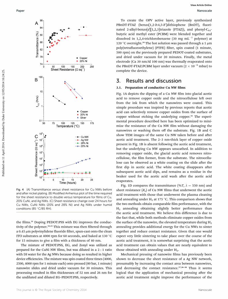
Fig. 4 (A) Transmittance versus sheet resistance for Cu NWs beforeand after nickel plating. (B) Modified Arrhenius plot of the time requiredfor the sheet resistance to double versus temperature for films of Cu,20% CuNi, and Ag NWs. (C) Sheet resistance change over 24 hours forCu NWs, CuNi NWs (20% and 28% Ni) and Ag NWs under humidconditions (85 �C/85 RH).
Paper Nanoscale
Publ
ishe
d on
11
Apr
il 20
14. D
ownl
oade
d by
Duk
e U
nive
rsity
on
12/0
5/20
14 1
6:24
:25.
View Article Online
the lms.31 Doping PEDOT:PSS with EG improves the conduc-tivity of the polymer.32,33 This mixture was then ltered througha 0.45 mmpolyvinylidene uoride lter, spun-cast onto the cleanITO substrates at 4000 rpm for 60 seconds, and baked at 130 �Cfor 15 minutes to give a lm with a thickness of 40 nm.
The mixture of PEDOT:PSS, EG, and Zonyl was utilized asprepared for the CuNi NW lms, but was diluted in a 2 : 1 ratiowith DI water for the Ag NWs because doing so resulted in higherdevice efficiencies. Themixture was spin coated three times (4000,2500, 4000 rpm for 1minute each) onto pressed (80 bar, 1 minute)nanowire slides and dried under vacuum for 30 minutes. Thisprocessing resulted in lm thicknesses of 52 nm and 26 nm forthe undiluted and diluted EG–PEDOT:PSS, respectively.
This journal is © The Royal Society of Chemistry 2014
To create the OPV active layer, previously synthesizedPBnDT-FTAZ (benzo[1,2-b:4,5-b0]dithiophene (BnDT), uori-nated 2-alkyl-benzo[d][1,2,3]triazole (FTAZ)), and phenyl-C61-butyric acid methyl ester (PCBM) were blended together anddissolved in 1,2,4-trichlorobenzene (30 mg mL�1 polymer) at120 �C overnight.34 The hot solution was passed through a 1 mmpoly(tetrauoroethylene) (PTFE) lter, spin coated (1 minute,500 rpm) on the previously prepared PEDOT-coated substrates,and dried under vacuum for 20 minutes. Finally, the metalelectrode (Ca 30 nm/Al 100 nm) was thermally evaporated ontothe PBnDT-FTAZ:PCBM layer under vacuum (2 � 10�6 mbar) tocomplete the device.
3. Results and discussion3.1. Preparation of conductive Cu NW lms
Fig. 1A depicts the dipping of a Cu NW lm into glacial aceticacid to remove copper oxide and the nitrocellulose le overfrom the ink from which the nanowires were coated. Thissimple procedure was inspired by previous reports that aceticacid can selectively remove copper oxides from the surface ofcopper without etching the underlying copper.35 The experi-mental procedure described here has been optimized to mini-mize the resistance of the Cu NW lm without damaging thenanowires or washing them off the substrate. Fig. 1B and Cshow TEM images of the same Cu NW taken before and aeracetic acid treatment. The 2–3 nm-thick layer of copper oxidepresent in Fig. 1B is absent following the acetic acid treatment,but the underlying Cu NW appears unscathed. In addition toremoving copper oxide, the glacial acetic acid removes nitro-cellulose, the lm former, from the substrate. The nitrocellu-lose can be observed as a white coating on the slide aer therst dip in acetic acid. The white coating disappears aersubsequent acetic acid dips, and remains as a residue in thebeaker used for the acetic acid wash aer the acetic acidevaporates.
Fig. 1D compares the transmittance (%T, l ¼ 550 nm) andsheet resistance (Rs) of Cu NW lms that underwent the aceticacid treatment with those that underwent the plasma cleaningand annealing under H2 at 175 �C. This comparison shows thatthe two methods obtain comparable lm performance, with theH2 annealing obtaining slightly better performance thanthe acetic acid treatment. We believe this difference is due tothe fact that, while both methods eliminate copper oxides fromthe surface of the nanowire, the elevated temperature during H2
annealing provides additional energy for the Cu NWs to sintertogether and reduce contact resistance. Given that one wouldexpect very little sintering to take place over the course of theacetic acid treatment, it is somewhat surprising that the aceticacid treatment can obtain values that are nearly equivalent tothose obtained with annealing under H2.
Mechanical pressing of nanowire lms has previously beenshown to decrease the sheet resistance of a Ag NW network,presumably by increasing the contact area between nanowires,and decreasing the contact resistance.27,36–38 Thus it seemslogical that the application of mechanical pressing aer theacetic acid treatment might improve the performance of the
Nanoscale
Nanoscale Paper
Publ
ishe
d on
11
Apr
il 20
14. D
ownl
oade
d by
Duk
e U
nive
rsity
on
12/0
5/20
14 1
6:24
:25.
View Article Online
electrode to be comparable to the performance of a Cu NW lmannealed under H2. The SEM images in Fig. 2A and B showthere is no discernable difference in the morphology of the CuNW lm before and aer acetic acid treatment. Aer pressingthe wires at 80 bar for 1 minute (Fig. 2C), the junctions betweenthe nanowires appear to be fused together and the averagesurface roughness (Ra) decreases from 78 nm to 37 nm.However, a graph of %T vs. Rs before and aer pressing (Fig. 2D)shows there is no improvement in performance aer pressing.This is due to the fact that both the sheet resistance and thetransmittance of the lm decrease aer pressing. For example,for a Cu NW lm treated with acetic acid with an initial sheetresistance of 89 U sq�1 at 93% T, the sheet resistance andtransmittance decreased to 61 U sq�1 and 91% T aer pressing.The decrease in %T is likely due to attening of the nanowiresduring the pressing process, which increases the area coverageof the nanowires, and decreases the light transmitted throughthe open areas of the network. Indeed, the Cu NWs appear to bemore cylindrical in Fig. 2B, and somewhat more rectangularand attened in Fig. 2C. Lowering or increasing the appliedpressure relative to 80 bar did not result in any improvedoptoelectronic performance (see Fig. S1A†). Fig. S1B† shows theattening of the nanowires was more pronounced at 160 barthan at 80 bar.
3.2. Electroless nickel plating
In order to protect the Cu NWs from oxidation, we have previ-ously demonstrated the electroless plating of nickel onto thenanowires while they are dispersed in solution,28 as well as theelectroplating of nickel onto the nanowires aer they aredeposited on a lm.39 Electroplating Ni onto Cu NWs aer lmformation avoids laborious centrifugation and washing steps,eliminates ethylene glycol waste, and prevents the aggregationof NWs due to the magnetic attraction between CuNi NWs insolution. However, electroplating is somewhat more compli-cated in that it requires the use of a current source, and isdifficult to apply uniformly over a large area due to the resis-tance of the nanowire lm. Here we explore a third method,electroless plating of nickel onto copper nanowire lms thatoffers the advantages of both previous methods with few of thedisadvantages.
Following acetic acid treatment, the Cu NW electrodes werebriey dipped into an activation solution containing Pd2+ beforebeing transferred to a nickel plating solution (Fig. 3A). Activa-tion of the surface of Cu with Pd has previously been shown tofacilitate the plating of Ni onto a Cu surface.40,41 We see noplating of Ni onto the Cu NWs if they are not rst exposed toPd2+. Although Pd is not an abundant, inexpensive element, solittle of the Pd is actually incorporated into the nanowires(0.00482 g m�2) that the contribution of the cost of Pd to thecost of the nanowire lms is less than two orders of magnitudesmaller than the cost of ITO lm ($0.13 per m2, see Table S1†).
A linear relationship between the time spent in the nickelsolution and the amount of nickel deposited on the Cu NWnetwork is shown in Fig. S2.† Aer 12.5 minutes in the platingsolution, the diameter of the resulting CuNi NWs increased
Nanoscale
from 67 � 15 nm to 90 � 31 nm (Fig. 3B). Dark eld opticalmicroscope images of the nanowire network before and aer20% nickel plating (Fig. 3C and D) show that the color of thenanowires changed from reddish to grey. The nickel coatingresulted in a small decrease in sheet resistance, but about a 4%drop in the transmittance (at l ¼ 550 nm). This drop in trans-mittance is consistent with previous results, and is due to theincrease in the diameter of the nanowires aer nickel coating.28
Fig. 4A shows a graph of transmittance (l ¼ 550 nm) versussheet resistance before and aer the nickel coating.
Fig. 4B shows coating the Cu NWs with 20% Ni gives them aresistance to oxidation comparable to Ag NWs. This plot showsthe time required for the sheet resistance of nanowire lms ofcomparable transmittance (85–87% T) to double (t1/2) aerbeing placed in a dry oven heated to a given temperature (75–150 �C). For example, it takes about 1 h for the sheet resistanceof a Cu NW lm to double at 105 �C, but this increases to 38 h ifthe NWs are coated with 20% Ni. The stability of the nanowirelms was also compared in a humidity chamber at 85 �C and85 � 3% RH (Fig. 4C). Under these conditions, Cu NW lmsbecame insulating in less than 1 h, 20% CuNi NWs were stablefor <5 h, and 28% CuNi NWs exhibited a stability similar to AgNW lms.
3.3. CuNi NW solar cell performance
One of the obstacles to the replacement of ITO with nanowirelms in OPVs is the greater surface roughness of nanowireelectrodes.42 The peak-to-valley surface roughness of nanowireelectrodes coated from solution and treated with acetic acid(Fig. 2B) is slightly less than two nanowire diameters, or 104nm. This surface roughness is nearly the same as the thicknessof a typical polymer active layer. As a result, many of the OPVdevices made with nanowire electrodes have exhibitedsmall shunt resistances, and correspondingly low OPVefficiencies.23,24,26,43,44
One approach to making a smooth nanowire electrodeinvolves transferring the nanowires from a donor substrate to apolymer, and in the process embedding them in the polymer.45
In one case, this was accomplished by spin coating a polymer(polyacrylate) over a lm of Ag NWs, photocuring the polymerlm, and peeling away the polymer lm to reveal a smooth (rmsroughness < 5 nm) surface containing the nanowires embeddedin the polymer lm.44 The best device made with this methodexhibited an efficiency of 3.28%.44 Peumans and co-workersachieved an efficiency of 4.2% by laminating Ag NWs into thesurface of PEDOT:PSS.42 However, transferring the nanowiresfrom one substrate to another is quite difficult to do with highdelity, and may result in low device yields in a productionenvironment.
We have found that comparable or greater device efficienciescan be achieved by optimizing the coating process forPEDOT:PSS over the nanowire lm. We have previouslyobtained device efficiencies of 2.8% and 2.5% on glass and PET,respectively, by coating a Ag NW lm with a single coating ofPEDOT:PSS with a thickness of 40 nm.23 Since then, we havefound that coating the nanowire lm three times with
This journal is © The Royal Society of Chemistry 2014

Paper Nanoscale
Publ
ishe
d on
11
Apr
il 20
14. D
ownl
oade
d by
Duk
e U
nive
rsity
on
12/0
5/20
14 1
6:24
:25.
View Article Online
PEDOT:PSS mixed with EG and a uorosurfactant allowed us toachieve device efficiencies nearly twice that of those obtainedpreviously. As the current PEDOT:PSS coating is not muchthicker than the ones used previously, we believe the reason forthe increase in device efficiency from the three-step coatingprocess is principally due to the fact that a more completecoating is achieved, thereby facilitating the transport of holes tothe metallic nanowires while preventing device shorts andelectron–hole recombination at the surface of the metalnanowires.
Fig. 5A and B show AFM images before and aer CuNi NWswere coated with PEDOT:PSS. Prior to testing the CuNi NWelectrodes in an OPV device, the lms were pressed (80 bar, 1minute) in an attempt to decrease the roughness of the nano-wire network. A nickel concentration of 28% was chosen toincrease the resistance of the nanowire lm to oxidation. The Ra
Fig. 5 AFM images of Cu NW films (A) before and (B) coating withPEDOT:PSS.
Fig. 6 (A) Diagram of the nanowire-based FTAZ BHJ solar cell. (B) Charactransparent electrode. (C) The transmittance of the transparent conducwavelength curves of the FTAZ BHJ solar cells with ITO, Ag NW, and Cu
This journal is © The Royal Society of Chemistry 2014
of the pressed CuNi NWs dropped from 52 nm to 18 nm aercoating PEDOT:PSS onto the nanowires.
Fig. 6A is a schematic illustrating the layers of the nisheddevice. FTAZ:PCBM denotes the blend of PBnDT-FTAZ andPCBM used as the active layer. This blend was chosen due to itspreviously demonstrated high performance in BHJ OPVsutilizing nanowires as the transparent electrode.23 Films of AgNWs (%T ¼ 76, Rs ¼ 14 U sq�1) and CuNi NWs (%T ¼ 80, Rs ¼36 U sq�1) were fabricated to have similar lm properties todetermine if the replacement of Ag with the lower-cost CuNiNWs would affect the performance of the OPV. Representativecurrent–voltage curves for the devices are shown in Fig. 6B andthe relevant photovoltaic characteristics are summarized inTable 1. Compared to the ITO reference, both nanowire baseddevices display lower short-circuit currents (JSC; J at V¼ 0), lowerll factor (FF), and slightly lower open circuit voltages (VOC; V atJ ¼ 0), resulting in lower device efficiencies.
Previous papers also show that the VOC for OPVs using AgNW lms is lower than ITO lms.12,23–25 This has previouslybeen attributed to the fact that Ag has a lower work function(4.3–4.7 eV)46–48 than ITO (4.7–5.0 eV),49–51 resulting in a
teristic J–V curves of solar cells with ITO, Ag NWs, and CuNi NWs as theting films and respective devices versus wavelength. (D) IPCE versusNi NW anodes under one sun condition (100 mW cm�2).
Table 1 Photovoltaic performance of the FTAZ BHJ solar cells
Anode JSC (mA cm�2) VOC (V) FF (%) h (%)
ITO 11.97 0.810 74.0 7.1Ag NW 10.18 0.776 63.4 5.0CuNi NW 9.98 0.767 63.5 4.9
Nanoscale

Nanoscale Paper
Publ
ishe
d on
11
Apr
il 20
14. D
ownl
oade
d by
Duk
e U
nive
rsity
on
12/0
5/20
14 1
6:24
:25.
View Article Online
greater barrier to the transport of holes out of the device.23
Compared to our previous work in which the VOC for OPVsusing nanowire lms as anodes was on average 59% of thoseobtained for ITO, the three step coating process has improvedthe VOC to be 96% (Ag NWs) and 95% (CuNi NWs) that of theITO reference. The slightly lower VOC observed for nanowirelms may be due to the fact that the coverage of PEDOT:PSSon the nanowires is not as uniform and pinhole-free as thecoating of PEDOT:PSS on ITO.
The lower JSC of the devices can be attributed to the lowertransmittance of the Cu NW and Ag NW lms relative to ITO.The JSC of the nanowire-based devices is roughly 20% lower thanthe ITO-based device, which is roughly equivalent to thedifference in the percent of incident light absorbed by thenanowire and ITO-based devices (see Table S2† and Fig. 6C).This inference is further supported by the correlation betweenthe transmittance of the lms and devices (Fig. 6C) with theincident photon to current efficiency (IPCE) of the devices(Fig. 6D). Thus the JSC of the nanowire-based devices can likelybe improved by improving the transmittance of the nanowirelms at a given sheet resistance.25,52
4. Conclusion
We have shown that simply dipping Cu NW lms in aceticacid makes them nearly as conductive as Cu NW lmsannealed under hydrogen. We have further introduced a lm-based electroless nickel plating process that gives Cu NWlms a stability comparable to Ag NW lms, even underhumid conditions. Finally, we have shown that BHJ OPVsusing lms of CuNi NWs as the transparent anode can achievea device efficiency of 4.9%, nearly equivalent to the 5% effi-ciency of a BHJ OPV utilizing Ag NWs as the transparentanode.
By simplifying the processing of Cu NW lms, we hope thiswork helps to remove existing hurdles to the wider practicalapplication of Cu NWs. That being said, the simple coat andheat processing used for Ag NWs remains easier than the pro-cessing necessary for Cu NWs, so there is still room for furthersimplication of the processing steps.13 In addition, althoughthe CuNi device efficiency of 4.9% is relatively high compared toprevious work, it is still lower than the 7.1% device efficiencyobtained for the device based on ITO. This issue can likely beaddressed by using lms composed of nanowires with higheraspect ratios, which exhibit a higher transmittance at the samesheet resistance.15,53
Acknowledgements
This work was supported in part by the National ScienceFoundation's (NSF's) Research Triangle MRSEC (DMR-1121107), an NSF CAREER award (DMR-1253534), EMD Milli-pore, and NSF grant no. ECCS-1344745. I.E.S. and P.F.F.acknowledge support by a fellowship from the GraduateCerticate Program in Nanoscience at Duke University.
Nanoscale
References
1 N. S. Lewis and D. G. Nocera, Proc. Natl. Acad. Sci. U. S. A.,2006, 103, 15729–15735.
2 C. Wadia, A. P. Alivisatos and D. M. Kammen, Environ. Sci.Technol., 2009, 43, 2072–2077.
3 C. J. M. Emmott, A. Urbina and J. Nelson, Sol. Energy Mater.Sol. Cells, 2012, 97, 14–21.
4 D. C. U.S. Geological Survey, Mineral Commodity Summaries,Indium, U.S. Department of the Interior, Washington, 2013,p. 2074.
5 D. C. U.S. Geological Survey, Mineral Commodity Summaries,Silver, U.S. Department of the Interior, Washington, 2013,p. 2146.
6 S. Kirchmeyer and K. Reuter, J. Mater. Chem., 2005, 15, 2077–2088.
7 A. Elschner and W. Lovenich, MRS Bull., 2011, 36, 794–798.
8 Z. Wu, Z. Chen, X. Du, J. M. Logan, J. Sippel, M. Nikolou,K. Kamaras, J. R. Reynolds, D. B. Tanner, A. F. Hebard andA. G. Rinzler, Science, 2004, 305, 1273–1276.
9 D. S. Hecht, L. B. Hu and G. Irvin, Adv. Mater., 2011, 23, 1482–1513.
10 C. Niu, MRS Bull., 2011, 36, 766–773.11 S. Bae, H. Kim, Y. Lee, X. Xu, J.-S. Park, Y. Zheng,
J. Balakrishnan, T. Lei, H. R. Kim, Y. I. Song, Y.-J. Kim,K. S. Kim, B. Ozyilmaz, J.-H. Ahn, B. H. Hong andS. Iijima, Nat. Nanotechnol., 2010, 5, 574–578.
12 J.-W. Lim, D.-Y. Cho, K. Eun, S.-H. Choa, S.-I. Na, J. Kimand H.-K. Kim, Sol. Energy Mater. Sol. Cells, 2012, 105,69–76.
13 M. Song, D. S. You, K. Lim, S. Park, S. Jung, C. S. Kim,D.-H. Kim, D.-G. Kim, J.-K. Kim, J. Park, Y.-C. Kang, J. Heo,S.-H. Jin, J. H. Park and J.-W. Kang, Adv. Funct. Mater.,2013, 23, 4177–4184.
14 J. Lee, P. Lee, H. Lee, D. Lee, S. S. Lee and S. H. Ko, Nanoscale,2012, 4, 6408–6414.
15 S. Ye, A. R. Rathmell, I. E. Stewart, Y.-C. Ha, A. R. Wilson,Z. Chen and B. J. Wiley, Chem. Commun., 2014, 50, 2562–2564.
16 H. Z. Guo, N. Lin, Y. Z. Chen, Z. W. Wang, Q. S. Xie,T. C. Zheng, N. Gao, S. P. Li, J. Y. Kang, D. J. Cai andD. L. Peng, Sci. Rep., 2013, 3, 8.
17 A. Kumar and C. Zhou, ACS Nano, 2010, 4, 11–14.18 L. Hu, H. Wu and Y. Cui, MRS Bull., 2011, 36, 760–765.19 D. C. U.S. Geological Survey, Mineral Commodity Summaries,
Copper, U.S. Department of the Interior, Washington, 2013,p. 2048.
20 A. R. Rathmell and B. J. Wiley, Adv. Mater., 2011, 23, 4798–4803.
21 A. R. Rathmell, S. M. Bergin, Y.-L. Hua, Z.-Y. Li andB. J. Wiley, Adv. Mater., 2010, 22, 3558–3563.
22 S. Ye, A. R. Rathmell, Y.-C. Ha, A. R. Wilson and B. J. Wiley,Small, 2014, 10, 1771–1778.
23 L. Q. Yang, T. Zhang, H. X. Zhou, S. C. Price, B. J. Wiley andW. You, ACS Appl. Mater. Interfaces, 2011, 3, 4075–4084.
This journal is © The Royal Society of Chemistry 2014
Paper Nanoscale
Publ
ishe
d on
11
Apr
il 20
14. D
ownl
oade
d by
Duk
e U
nive
rsity
on
12/0
5/20
14 1
6:24
:25.
View Article Online
24 D. S. Leem, A. Edwards, M. Faist, J. Nelson,D. D. C. Bradley and J. C. de Mello, Adv. Mater., 2011,23, 4371–4375.
25 N. Yong-Jin, K. Seok-Soon, K. Tae-Wook and N. Seok-In,Semicond. Sci. Technol., 2013, 28, 125008.
26 W. Gaynor, J. Y. Lee and P. Peumans, ACS Nano, 2010, 4,30–34.
27 C. Sachse, N. Weiß, N. Gaponik, L. Muller-Meskamp,A. Eychmuller and K. Leo, Adv. Eng. Mater., 2014, DOI:10.1002/aenm.201300737.
28 A. R. Rathmell, M. Nguyen, M. F. Chi and B. J. Wiley, NanoLett., 2012, 12, 3193–3199.
29 B. Wiley, Y. G. Sun and Y. N. Xia, Langmuir, 2005, 21, 8077–8080.
30 S. M. Bergin, Y. H. Chen, A. R. Rathmell, P. Charbonneau,Z. Y. Li and B. J. Wiley, Nanoscale, 2012, 4, 1996–2004.
31 M. Vosgueritchian, D. J. Lipomi and Z. Bao, Adv. Funct.Mater., 2012, 22, 421–428.
32 J. Ouyang, C. W. Chu, F. C. Chen, Q. Xu and Y. Yang, Adv.Funct. Mater., 2005, 15, 203–208.
33 J. Ouyang, Q. Xu, C.-W. Chu, Y. Yang, G. Li and J. Shinar,Polymer, 2004, 45, 8443–8450.
34 S. C. Price, A. C. Stuart, L. Yang, H. Zhou and W. You, J. Am.Chem. Soc., 2011, 133, 4625–4631.
35 K. L. Chavez and D. W. Hess, J. Electrochem. Soc., 2001, 148,G640–G643.
36 T. Tokuno, M. Nogi, M. Karakawa, J. T. Jiu, T. T. Nge, Y. Asoand K. Suganuma, Nano Res., 2011, 4, 1215–1222.
37 J. H. Choi, J. P. Kar, D. Y. Khang and J. M. Myoung, J. Phys.Chem. C, 2009, 113, 5010–5013.
38 L. B. Hu, H. S. Kim, J. Y. Lee, P. Peumans and Y. Cui, ACSNano, 2010, 4, 2955–2963.
39 Z. Chen, A. R. Rathmell, S. Ye, A. R. Wilson and B. J. Wiley,Angew. Chem., Int. Ed., 2013, 52, 13708–13711.
This journal is © The Royal Society of Chemistry 2014
40 F. Z. Kong, X. B. Zhang, W. Q. Xiong, F. Liu, W. Z. Huang,Y. L. Sun, J. P. Tu and X. W. Chen, Surf. Coat. Technol.,2002, 155, 33–36.
41 J. F. Rohan, G. O'Riordan and J. Boardman, Appl. Surf. Sci.,2002, 185, 289–297.
42 W. Gaynor, G. F. Burkhard, M. D. McGehee and P. Peumans,Adv. Mater., 2011, 23, 2905–2910.
43 J. Y. Lee, S. T. Connor, Y. Cui and P. Peumans, Nano Lett.,2008, 8, 689–692.
44 Z. B. Yu, L. Li, Q. W. Zhang, W. L. Hu and Q. B. Pei, Adv.Mater., 2011, 23, 4453–4457.
45 X. Y. Zeng, Q. K. Zhang, R. M. Yu and C. Z. Lu, Adv. Mater.,2010, 22, 4484–4488.
46 M. Methfessel, D. Hennig and M. Scheffler, Phys. Rev. B:Condens. Matter Mater. Phys., 1992, 46, 4816–4829.
47 CRC Handbook of Chemistry and Physics, CRC Press, 2008.48 R. E. Hummel, Electronic Properties of Materials, Springer-
Verlag, New York, 3rd edn, 2001.49 K. X. Steirer, P. F. Ndione, N. E. Widjonarko, M. T. Lloyd,
J. Meyer, E. L. Ratcliff, A. Kahn, N. R. Armstrong,C. J. Curtis, D. S. Ginley, J. J. Berry and D. C. Olson, Adv.Eng. Mater., 2011, 1, 813–820.
50 E. L. Ratcliff, A. Garcia, S. A. Paniagua, S. R. Cowan,A. J. Giordano, D. S. Ginley, S. R. Marder, J. J. Berry andD. C. Olson, Adv. Eng. Mater., 2013, 3, 647–656.
51 M. D. Irwin, J. D. Servaites, D. B. Buchholz, B. J. Leever, J. Liu,J. D. Emery, M. Zhang, J. H. Song, M. F. Durstock,A. J. Freeman, M. J. Bedzyk, M. C. Hersam, R. P. H. Chang,M. A. Ratner and T. J. Marks, Chem. Mater., 2011, 23,2218–2226.
52 S. K. Hau, H.-L. Yip, J. Zou and A. K. Y. Jen, Org. Electron.,2009, 10, 1401–1407.
53 R. M. Mutiso, M. C. Sherrott, A. R. Rathmell, B. J. Wiley andK. I. Winey, ACS Nano, 2013, 7, 7654–7663.
Nanoscale