Embed Size (px)
Citation preview
Nanoscale characterization with
scattering-type scanning near-
field infrared microscopy
Gergely Németh
Supervisors: Katalin Kamarás, Áron Pekker

Outline
• Motivation, why do we need near fields?
• Principles of s-SNOM technique
• Measurements on carbon nanotubes and
hybrid systems
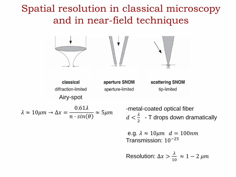
Spatial resolution in classical microscopy
and in near-field techniques
𝜆 ≈ 10𝜇𝑚 → Δ𝑥 =0.61𝜆
𝑛 ⋅ 𝑠𝑖𝑛 𝜃≈ 5𝜇𝑚
-metal-coated optical fiber
𝑑 <𝜆
2- T drops down dramatically
e.g. 𝜆 ≈ 10𝜇𝑚 𝑑 = 100𝑛𝑚Transmission: 10−25
Resolution: Δ𝑥 >𝜆
10≈ 1 − 2 𝜇𝑚
Airy-spot

s-SNOM principles
• Metal-coated AFM tip
• Evanescent EM field at a apex of
the tip
• Very close to the sample
• Near field polarizes the sample
• Interaction results scattered EM
waves
• 𝜆0 ≫ characteristic sizes of the tip
• Electrostatic problem at each timestep
• Incoming light is polarized parallel to the tip axis
• 𝑝 = 𝛼 ⋅ 𝐸0- induced dipole moment in the tip
• Mirror dipole in the sample: 𝑝′ = 𝛽𝑝 → 𝛽 =𝜖−1
𝜖+1
𝐸𝑠 = 𝜎𝐸0 𝜎 = 𝑠 ⋅ 𝑒𝑖𝜑

Only a small part of the detected light originates from the near-field interaction
- Airy spot is few microns, near-field volume is few of 10 nm-s
- Background: direct scattering from tip shaft, reflection, scattering from surface
roughness
- Incoming + reflected beam → interference → standing waves
Solution: AFM works in tapping mode at Ω frequency + demodulation @ 𝑛Ω
𝐼 = 𝐸𝐵 + 𝐸𝑁2 𝐸𝐵
2 + 𝐸𝑁2 + 2𝐸𝑁𝐸𝐵 still contains 𝐸𝐵

𝑠𝑛 = 𝐶𝑛Ω+𝑀2 + 𝐶𝑛Ω+2𝑀
2
𝜑𝑛 = arctan𝐶𝑛Ω+𝑀
𝐶𝑛Ω+2𝑀
𝐸𝑇 – total field
𝐸𝑁 – near-field signal
𝐸𝐵 – background scattering
𝐸𝑅 – phase-modulated
reference beam
N. Ocelic, A.Huber, R. Hillenbrand, Appl. Phys. Lett. 89, 101124 (2006).
𝐴𝑀 ≈ 0.21𝜆0

Demodulation at higher harmonics
AFM topography
(20 nm high Au islands)
O1 (strong background
scattering)O3 (clear near-field)

Study on single-walled carbon nanotubes
H. M. Tóháti, Á. Pekker, B. Á. Pataki, Zs. Szekrényes, and K. Kamarás, Eur. Phys. J. B 87, 126–1–6 (2014).
Properties are defined by their structure
• Semiconducting
• Metallic
Selective production is important
• Qualify these methods
• Different optical properties

Analytical model
Analytical calculations based on extended finite dipole model (EFDM)
• Substrate-particle-tip system
• Approximated with numerous charges
generated by the incident E field
• 𝑝0, 𝑝1, 𝑝2 describe electric field
of the nanoparticle
• 𝑝 = 𝛼𝑧 ⋅ 𝐸𝑙𝑜𝑐• Nanotubes are cylinder-like objects
• Approximated with a prolate ellipsoid
• The following expression was used:
𝛼𝑧 =𝜖 − 1
1 + 𝑁𝑧 𝜖 + 1𝜖 = 𝜖1 + 𝑖 ⋅ 𝜖2 - complex dielectric function
𝑁𝑧– depolarization factor
𝑝𝑒𝑓𝑓 = −2𝑄0𝐿 − 𝑄𝑖𝑛𝑑𝐿 + 𝑃1 + 𝑃2 + 𝑃3 + 𝑝0 + 𝑝1 + 𝑝2𝑝𝑒𝑓𝑓 ∝ 𝜎
Simulating the tapping mode: 𝑧 = (𝐻 + 𝐴(1 − cos Ωt ) → demodulation→𝜎𝑛 = 𝑠𝑛𝑒𝑖𝜑𝑛
A. Cvitkovic, Ph.D. thesis, Technische Universit¨at München (2009). J.Venermo and A. Sihvola, J. Electrostat. 63, 101–117 (2005).
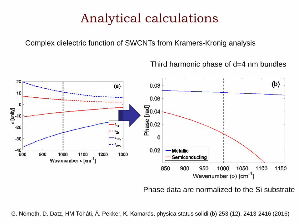
Analytical calculations
Complex dielectric function of SWCNTs from Kramers-Kronig analysis
Phase data are normalized to the Si substrate
Third harmonic phase of d=4 nm bundles
G. Németh, D. Datz, HM Tóháti, Á. Pekker, K. Kamarás, physica status solidi (b) 253 (12), 2413-2416 (2016)

Aligned SWCNT samples
Before
After breaking metallic SWNTs
• CNT array for transistor fabrication
• Samples from University of Tokyo
• Group of Prof. Shigeo Maruyama
• Horizontally aligned nanotubes
grown by CVD
• Transferred onto Si/SiO2 substrate
• Gold contacts
• Metallic nanotubes were destroyed
• Electrical breakdown technique
K. Otsuka, T. Inoue, S. Chiashi, and S. Maruyama, Nanoscale 6,
8831 (2014).
P. G. Collins, M. S. Arnold, P. Avouris, Science 292, 706-709 (2001).
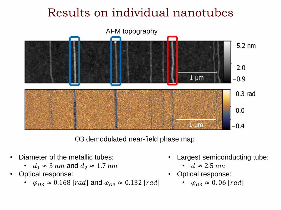
Results on individual nanotubes
• Diameter of the metallic tubes:
• 𝑑1 ≈ 3 𝑛𝑚 and 𝑑2 ≈ 1.7 𝑛𝑚• Optical response:
• 𝜑𝑂3 ≈ 0.168 [𝑟𝑎𝑑] and 𝜑𝑂3 ≈ 0.132 [𝑟𝑎𝑑]
• Largest semiconducting tube:
• 𝑑 ≈ 2.5 𝑛𝑚• Optical response:
• 𝜑𝑂3 ≈ 0. 06 [𝑟𝑎𝑑]
AFM topography
O3 demodulated near-field phase map

Spectral behaviour of individual tubes
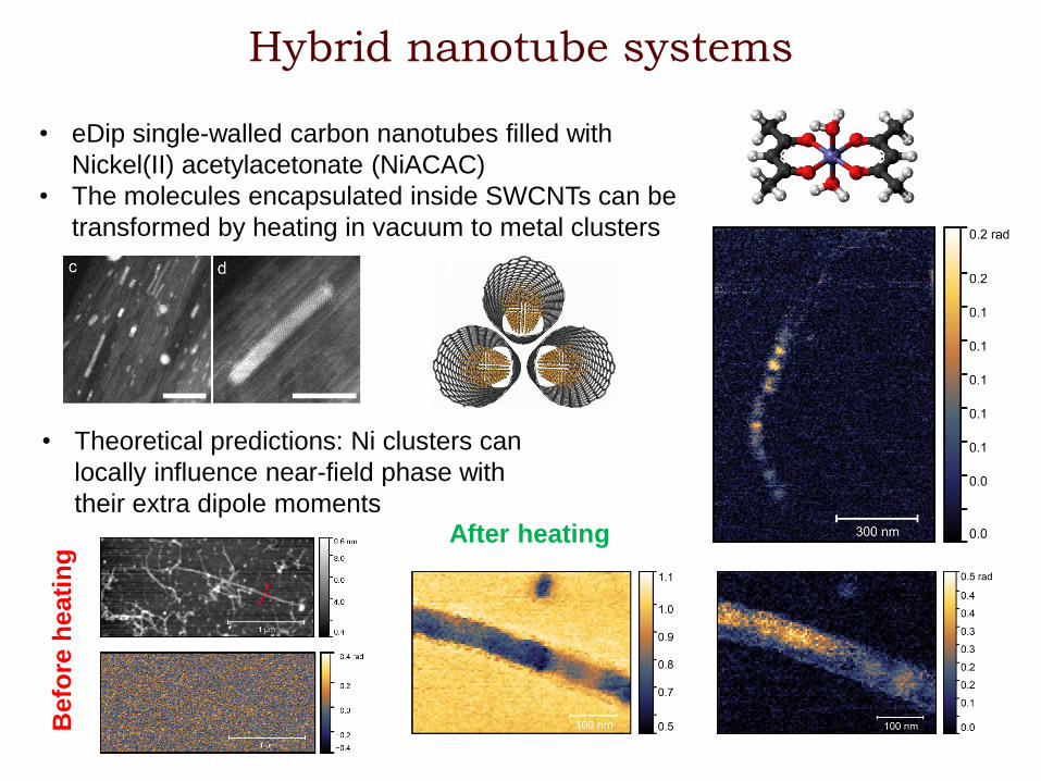
Hybrid nanotube systems
• eDip single-walled carbon nanotubes filled with
Nickel(II) acetylacetonate (NiACAC)
• The molecules encapsulated inside SWCNTs can be
transformed by heating in vacuum to metal clusters
• Theoretical predictions: Ni clusters can
locally influence near-field phase with
their extra dipole moments
Befo
reh
eati
ng
After heating

Conclusions
Spatial resolution ≈ 10 − 20𝑛𝑚Sensitivity level is much higher ≈ 1𝑛𝑚 → 𝑆𝑊𝐶𝑁𝑇𝑠
Signal from difference in polarizability → many different sources
• Collective excitations → BNNTs
• Molecular vibrations
• Charge density difference
• Material specific recognition
Huge variability and possibilities
• We are open for collaboration
Acknowledgement
BME
• Koppa Pál
• Sepsi Örs
University of Tokyo
• Group of Prof. Shigeo
Maruyama
University of Nottingham
• Group of Prof. Andrei N.
Khlobystov

Thank you for your attention!

Spectroscopy with s-SNOM device
In its original setup, the s-SNOM device is a microscope
Capable of measurements on a fixed wavenumber (e.g. CNTs)
Modification for spectrum measurements
Need to set:
• wavenumber
• amplitude of vibrating mirror

Good candidates for spectroscopic
measurements
• Limited spectral range due to available lasers:
• Tunable quantum cascade lasers from 950-1050 cm-1 and 1320-
1450 cm-1.
• Second laser is ideal for boron nitride.
Real
Imaginary

Boron nitride structures
Many different allotropes:
http://nanotechweb.org/cws/article/tech/46378
https://www.sciencelearn.org.nz/images/2208-boron-nitride

Phonon-polariton modes in BNNTs
Far-field absorption peak at 1375 cm-1
This peak corresponds to a TO mode (in-plane, longitudinal stretch).

Individual MWBNNT under AFM

As-prepared spectrum of BNNT

Cleaning procedure
• Opening and cleaning procedure for BNNTs
• Ultimate goal: filling with molecules
Walker, K.E., Rance, G.A., Pekker, Á., Tóháti, H.M., Fay, M.W.,
Lodge, R.W., Stoppiello, C.T., Kamarás, K. and Khlobystov, A.N.,
Small Methods, 1 (9), 1700184 (2017).
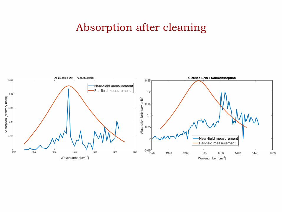
Absorption after cleaning

Near-field spectrum after cleaning

Mapping of impurities on a single
nanotube
@1380 cm-1 @1430 cm-1
Mapping of localized
phonon-polariton
modes with 10 nm
spatial resolution
D. Dániel, G. Németh, H. M. Tóháti, Á. Pekker and K. Kamarás, physica status solidi (b), 1700277 (2017).

Outlook
Mapping of impurities in hBN?

Outlook
Mapping of impurities in hBN?

Outlook: hyperbolic phonon-polaritons
Interference patterns on edges due to reflection
S. Dai et al., Science 343, 1125 (2014)

Outlook: hyperbolic phonon-polaritons
Interference patterns on edges due to reflection
D. Datz unpublished