Embed Size (px)
Citation preview

LUND UNIVERSITY
PO Box 117221 00 Lund+46 46-222 00 00
Nanophotonics in absorbing III-V nanowire arrays
Anttu, Nicklas
Published: 2013-01-01
Link to publication
Citation for published version (APA):Anttu, N. (2013). Nanophotonics in absorbing III-V nanowire arrays
General rightsCopyright and moral rights for the publications made accessible in the public portal are retained by the authorsand/or other copyright owners and it is a condition of accessing publications that users recognise and abide by thelegal requirements associated with these rights.
• Users may download and print one copy of any publication from the public portal for the purpose of privatestudy or research. • You may not further distribute the material or use it for any profit-making activity or commercial gain • You may freely distribute the URL identifying the publication in the public portalTake down policyIf you believe that this document breaches copyright please contact us providing details, and we will removeaccess to the work immediately and investigate your claim.

Download date: 10. Jun. 2018
Nanophotonics in absorbing III-V nanowire arraysNICKLAS ANTTU DIVISION OF SOLID STATE PHYSICS | DEPARTMENT OF PHYSICS | LUND UNIVERSITY

Nanophotonics in absorbing III-V nanowire arrays
Nicklas Anttu
Doctoral Thesis
2013
Division of Solid State Physics Department of Physics
Lund University
Academic Dissertation which, by due permission of the Faculty of Engineering at Lund University, will be publicly defended on Friday,
June 14th, 2013 at 14.00 in Rydbergsalen, Sölvegatan 14, Lund, for the degree of Doctor of Philosophy in Engineering.
Faculty opponent: Prof. Eli Yablonovitch, University of California, Berkeley, USA.
200

Nanophotonics in absorbing III-V nanowire arrays
Nicklas Anttu
Doctoral Thesis 2013
Division of Solid State Physics Department of Physics
Lund University

Copyright © Nicklas Anttu 2013
Division of Solid State Physics Department of Physics Lund University P.O. Box 118 SE-221 00 Lund Sweden ISBN 978-91-7473-549-9 (print) ISBN 978-91-7473-550-5 (pdf) Printed in Sweden by Media-Tryck, Lund University Lund 2013
A part of FTI (the Packaging and A part of FTI (the Packaging and Newspaper Collection Service)Newspaper Collection Service)

v
Table of contents Preface vii
Acknowledgements ix
Abstract xiii
Populärvetenskaplig sammanfattning xv
List of papers xvii
1 Introduction 1
1.1 Semiconductors 3 1.1.1 III-V semiconductors 4 1.1.2 Lattice matching in heterostructures 4
1.2 Nanowires 5 1.2.1 Interaction of light with nanowire arrays 6
2 Measurement of optical properties of nanowire arrays 9
2.1 Reflectance measurements 9 2.1.1 Specular reflectance 10 2.1.2 Total reflectance 12 2.1.3 Dependence on the size of the measurement spot 12
2.2 Transmittance measurements 13
2.3 Absorptance measurements 14
3 Modeling the optical response of nanowire arrays 17
3.1 Geometrical optics 17
3.2 Wave optics 18
3.3 Electromagnetic optics 18
3.4 Choice of the optical description 19
3.5 Validity of the electromagnetic modeling 19
3.6 Numerical methods for electromagnetic optics 19 3.6.1 Fourier modal method 20 3.6.1.1 Scattering matrix method 23 3.6.1.2 Computational time and convergence rate 23
4 Optical properties of absorbing nanowire arrays 25
4.1 Geometrical optics limit 25
4.2 Electrostatic limit 26 4.2.1 Effective medium theory 27

vi
4.2.2 Absorptance in the electrostatic limit 27 4.2.3 Reflectance in the electrostatic limit 28 4.2.4 Enhanced absorption by dielectric shell 29
4.3 Nanophotonic response of nanowire arrays 29 4.3.1 Silicon nanowire arrays 31 4.3.2 Direct band-gap III-V nanowire arrays 31 4.3.3 Comparison between silicon and III-V nanowire arrays 32 4.3.4 Nanocones 33 4.3.5 Nanophotonic resonances 34
5 Applications 39
5.1 Measurement of nanostructure dimensions 39
5.2 Investigation of material properties 42
5.3 Photodetection 44
5.4 Solar cells 45 5.4.1 Emission of light in solar cells 47
6 Conclusions 49 References 51

vii
Preface In this thesis, the results of my research on nanophotonics in nanowire arrays are presented. The contributions to the scientific field are contained in the eleven articles and manuscripts appended to the back of the thesis. At the beginning of the thesis, an introductory part is included. The aim with that introduction is to give a scientific background to the appended papers, which are cited as [Paper I-XI] there and listed below.


ix
Acknowledgements The research we perform in academia is often summarized in compact and brief reports that are, in the best of cases, published in scientific journals. Such reports leave little space for explaining the interaction between people that occurs in the background of the research. The work presented in this thesis would not have been possible to perform without the support from a large number of individuals.
First, I am grateful for the guidance and support I received from Prof. Hongqi Xu. I believe that I evolved toward a more self-confident scientist during his supervision.
Next, I would like to thank my supervisors Prof. Mats-Erik Pistol and Prof. Lars Samuelson. The research environment Lars has created with his enthusiasm and drive for new discoveries within nanoscience is truly impressive. I feel lucky for having had the opportunity to take part in some of the research projects initiated by him. The meetings I have had with Mats-Erik in his role as main supervisor have been a delight. I think that he has a very good view on science and an entertaining attitude toward life in general.
The many research collaborations with Dr. Ulf Håkanson have been a true pleasure. I will never be able to pay back the time he has spent guiding me. Furthermore, he managed to motivate me during the long days when things did not seem to progress at all neither at the office nor outside the office.
During the projects with Dr. Magnus Borgström, I saw a very professional and efficient attitude toward research. At the same time, the meetings were still entertaining and a great deal of fun. I am grateful to him for pushing me to become more efficient at summarizing our research results and moving swiftly toward publication.
I had the joy to get to know Dr. Phillip Wu who always showed a very nice and positive attitude to both research and life. We worked together in Lund for less than one year before he moved back to the States, but even during that short time I learned and changed a great deal. I wonder every now and then how much we could have accomplished if more time would have been given in Lund and how many more barbecue parties we would have had.
From the discussions and collaboration with Dr. Sebastian Lehmann, I learned a great deal, especially about nanowire growth and stringent approach to manuscript writing. The discussions we had about the calibration of the measurements in the scanning electron microscope and the many, many re-measurements of the same samples are stuff for legends. I think that the decision for you, me, and Phillip to work together on the project was a great one.
I worked with Dr. Jesper Wallentin on just one project, the European Union AMON-RA project for nanowire solar cells. However, for that single project, we had a
x
countless amount of meetings, sent 700 emails to each other, and worked through a multitude of manuscript versions. During that collaboration I believe that I sharpened my skills and became more efficient at conducting research: Merely observing the working pattern of Jesper teaches you a lot. I would at this point like to thank also the other participants of the AMON-RA project, especially Prof. Knut Deppert for excellent project coordination; and Damir Asoli, Dr. Ingvar Åberg, Dr. Maria Huffman, and Dr. Martin Magnusson for the work done at Sol Voltaics.
Together with Magnus Heurlin I had the great pleasure of combining modeling with experiments to measure nanowires in new ways. The short and reoccurring planning and analysis meetings have been a great deal of fun.
I truly enjoyed the collaboration with Dr. Johannes Svensson on nanowire photodetectors. For the physicist in me, it was a feast to see resonances show up in both experiments and modeling. The level of enthusiasm Johannes shows is remarkable and inspires me for a long time after each meeting.
During the many meetings and projects with Dr. Arkady Yartzev and Dr. Azhar Iqbal from the Department of Chemical Physics, I had the pleasure to discuss physics in depth. I also enjoyed the many possibilities for training my argumentation technique.
Within the NANORSUN project, I got the opportunity to work with Reza Sanatinia and Dr. Srinivasan Anand from KTH on the measurement and modeling of nanowire arrays. It was a great deal of fun to work with researchers that conduct very similar research as I do. I think that we complemented each other well.
When I started at the Division of Solid State Physics, I joined the mesoscopic physics group. There, I had the pleasure to get to get to know Dr. Daniel Wallin, Dr. Jie Sun, Dr. Marcus Larsson, and Dr. Henrik Nilsson from whom I learned a lot about research. From that group, Dr. Patrik Brusheim should be especially acknowledged for his great support during the start of my research endeavors.
Later I joined the Optics/Nanomechanics group. There, the interaction with Prof. Anders Gustafsson, Prof. Bo Monemar, Prof. Lars Montelius, Prof. Hongxing Xu, Prof. Håkan Pettersson, Dr. Monica Lexholm, Dr. Struan Gray, Carl Ellström, and Dr. Niklas Sköld taught me a lot about nanoscience and nano-optics.
I would also like to thank the technical and administrative staff at the division for making things run smoothly. I am especially grateful that Dr. Mariusz Graczyk showed me the thin-film analyzer in the cleanroom (that analyzer was not listed among the tools in the lab, and without it, much of the research presented in this thesis could not have been performed).
At the division there is also a large number of people who affected my research even if we were not explicitly involved in common research projects. During the first years I spent in room C263a, I had the pleasure to meet a large number of master students and guest researchers. I would like to mention especially Ricardo Andrade, Laura Barrutia Poncela, Anna Jansson, Martin Frimmer, Michael Wolff, and Ivan Karlsson who made

xi
the time spent at the office a joy with many discussions about research and other matters.
The move one year ago to room B107 brought me, Cassandra Niman, Henrik Persson, and Dr. Sebastian Lehmann together on a daily basis. This became a very well functioning office with an open atmosphere. I have had the pleasure to get to know both Cassandra and Henrik also outside the walls of the university.
I would like to thank David Lindgren for good company during lunches at Finn Inn, optics discussions, and great support at the office in general, Sofia Fahlvik-Svensson, Sepideh Gorji Ghalamestani, Dr. Karla Hillerich, Mercy Lard, and Dr. Maria Messing for giving much needed advice in research and non-research related issues, Kilian Mergenthaler for optics discussions and good barbecue sessions, Daniel Jacobsson for fun discussions about nanowire growth and support at the office, Gustav Nylund for discussions at the office as well as occasionally on the golf course, Guangyao Huang for many very interesting discussions, Dr. Zhiqiang Guan for the fun plasmonics projects, Andreas Jönsson, Susanne Norlén, Linda Johansson, Pardis Sahafi, Sofia Johansson, Fangfang Yang, Dr. Sandeep Kumar, Waldomiro Paschoal, Mingtang Deng, Chunlin Yu, Dr. Martina Balaz, and Regina Schmitt for spreading a positive atmosphere at and around the division, Jan-Göran Gluschke for trying to explain how to take matters less seriously, Bahram Ganjipour and Alexander Berg for showing what a dedicated attitude toward research looks like, Neimantas Vainorius for spot-on comments on tricky issues and an endless drive for new measurements, Mahtab Aghaeipour for the prospect of continuing modeling in the optics group, Vishal Jain and Ali Nowzari for interesting discussions about processing and device physics, Dr. Jonas Johansson for coordinating the graduate studies, Dr. Carina Fasth for the fun we had teaching courses where I at the same time learned a lot about solid state physics, Dr. Kristian Storm and Dr. Kimberly Dick Thelander for very promising start of on-going projects, Prof. Heiner Linke for good scientific suggestions and an efficient leadership of the division, and Dr. Dan Hessman for answering many of the questions I have had about optics and for all the fun we have had teaching a variety of courses.
Maciek Borysiuk, our training sessions at the gym and your morbid humor are a great mix.
Anil Dey and Dr. Fredrik Boxberg, thank you for all the support you have given during the fun and easy days as well as during the long and darker days.
Dr. Bernhard Mandl, you always offered an honest perspective to research and life. I am really happy that we did not lose contact after you moved back to Austria.
Johannes Walter and Mats Göransson, our golf rounds are a great deal of fun and a very good balance to the research-heavy surrounding of the university.
Joel Persson, Henrik Andersson, and Lars Pedersen, whenever we get together I have a blast. I just wish that you had chosen to move to southern Sweden instead of Stockholm after Umeå.

xii
Peter Nilsson, thank you for the listening and the support.
I would like to thank Johan Sandin and Marinus Wallgren, whom I got to know already in Haparanda, for always supporting me and for offering an honest view on matters.
Luna, I know that it has been for a short while yet, but each of those days has been great. You are truly one of a kind.
I would like to end by thanking my brother, my mother, and my father for unconditionally supporting me.
xiii
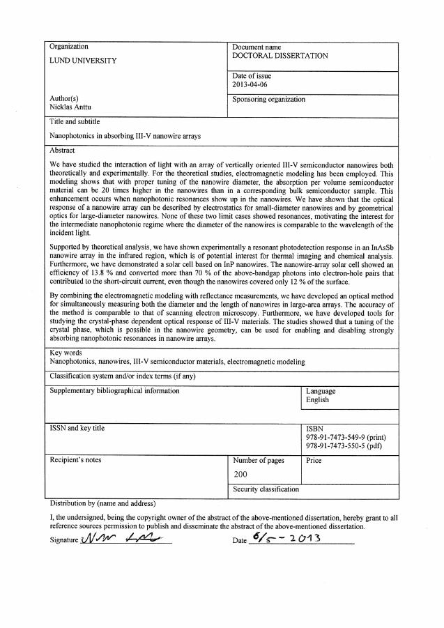
Abstract We have studied the interaction of light with an array of vertically oriented III-V semiconductor nanowires both theoretically and experimentally. For the theoretical studies, electromagnetic modeling has been employed. This modeling shows that with proper tuning of the nanowire diameter, the absorption per volume semiconductor material can be 20 times higher in the nanowires than in a corresponding bulk semiconductor sample. This enhancement occurs when nanophotonic resonances show up in the nanowires. We have shown that the optical response of a nanowire array can be described by electrostatics for small-diameter nanowires and by geometrical optics for large-diameter nanowires. None of these two limit cases showed resonances, motivating the interest for the intermediate nanophotonic regime where the diameter of the nanowires is comparable to the wavelength of the incident light.
Supported by theoretical analysis, we have shown experimentally a resonant photodetection response in an InAsSb nanowire array in the infrared region, which is of potential interest for thermal imaging and chemical analysis. Furthermore, we have demonstrated a solar cell based on InP nanowires. The nanowire-array solar cell showed an efficiency of 13.8 % and converted more than 70 % of the above-bandgap photons into electron-hole pairs that contributed to the short-circuit current, even though the nanowires covered only 12 % of the surface.
By combining the electromagnetic modeling with reflectance measurements, we have developed an optical method for simultaneously measuring both the diameter and the length of nanowires in large-area arrays. The accuracy of the method is comparable to that of scanning electron microscopy. Furthermore, we have developed tools for studying the crystal-phase dependent optical response of III-V materials. The studies showed that a tuning of the crystal phase, which is possible in the nanowire geometry, can be used for enabling and disabling strongly absorbing nanophotonic resonances in nanowire arrays.

xv
Populärvetenskaplig sammanfattning Den mänskliga civilisationen har en önskan att kontrollera ljusets växelverkan med materia. Genom bättre förståelse av hur ljuset beter sig kan man till exempel öka energieffektiviteten i optoelektroniska komponenter. I dessa komponenter kopplas ljusets optiska egenskaper ihop med de elektriska egenskaperna hos materialen i komponenterna. Till exempel i dagens mest avancerade solceller omvandlas mer än 40% av inkommande solljuset direkt till elektricitet, en av de mest användbara formerna av energi. Vidare, i de mest känsliga fotodetektorerna går det att detektera enskilda fotoner, ljusets minsta beståndsdelar.
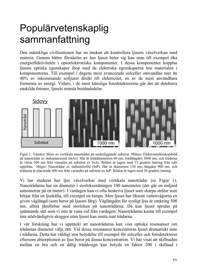
Figur 1. Vänster: Skiss av vertikala nanotrådar på underliggande substrat. Mitten: Elektronmikoskopibild på nanotrådar av indiumarsenid (InAs). Här är trådddiametern 60 nm, trådlängden 3600 nm, och trådarna är växta 500 nm från varandra på substrat av InAs. Bilden är tagen med 15 graders lutning från rakt uppifrån. Höger: Nanotrådar av indiumfosfid (InP). Här är diametern 130 nm, längden 900 nm, och trådarna är placerade 400 nm från varandra på substrat av InP. Bilden är tagen med 30 graders lutning.
Vi har studerat hur ljus växelverkar med vertikala nanotrådar (se Figur 1). Nanotrådarna har en diameter i storleksordningen 100 nanometer (det går en miljard nanometrar på en meter). I vardagen kan vi ofta beskriva ljuset som skarpa strålar som börjar från en ljuskälla, till exempel en lampa. Men ljuset har liksom vattenvågorna en given våglängd (som beror på ljusets färg). Våglängden för synligt ljus är omkring 500 nm, alltså jämförbar med storleken på nanotrådarna. Då kan ljuset spridas på spännande sätt som vi inte är vana vid från vardagen: Nanotrådarna kastar till exempel inte nödvändigtvis skuggor utan ljuset kan smita runt trådarna.
I vår forskning har vi upptäckt att nanotrådarna kan visa optiska resonanser om trådarnas diameter väljs rätt. Vid dessa resonanser koncentreras ljuset dramatiskt inne i trådarna. Detta har väldigt stor betydelse till exempel för solceller och fotodetektorer eftersom absorptionen av ljus beror på denna koncentration. Vi har visat att skillnaden mellan en bra och en dålig tråddesign kan betyda en faktor 200 i skillnad i

xvi
materialbehov: Med rätt design krävs det mindre mängd material i nanotråds-komponenter än i konventionella tunna filmer som är nuvarande standard inom teknikindustrin. Vi har genom experimentell och teoretisk forskning tagit fram detaljerade riktlinjer för effektiv hantering av ljus i nanotrådar. Vi har visat experimentellt hur nanotrådar kan användas för effektiva solceller. Vidare har vi visat hur nanotrådar kan användas för att detektera infrarött ljus, ett våglängdsområde av stort intresse för värmekameror och för spårning av kemikalier. Våra resultat bäddar för ökad användning av nanotrådar i energieffektiva och högpresterande optoelektroniska komponenter.
Mer detaljerat kommer det ursprungliga vetenskapliga intresset för att använda nanotrådar inom optoelektronik till stor del från nanotrådarnas materialegenskaper. Vi har koncentrerat våra studier på III-V halvledare där det ingår atomer från grupp III och grupp V från det periodiska systemet. Varje halvledande material har sitt specifika så kallade bandgap. Bandgapet anger vid vilken fotonenergi (det vill säga, vid vilken färg av ljuset) halvledaren börjar absorbera ljus märkbart. Genom att variera bandgapet med materialval kan man alltså påverka starkt hur ljuset växelverkar med materialet. III-V halvledare är väldigt användbara till detta ändamål eftersom de spänner ett stort våglängdsområde med sina bandgap.
Vanligtvis är man ute efter rena, kristallina material till optoelektroniska tillämpningar för att ha så få störningspunkter som möjligt inne i komponenterna. Varje kristallint material har sin specifika kristallkonstant som anger avståndet mellan atomerna i det atomgitter som utgör materialet. I optoelektroniska komponenter kombinerar man ofta olika (halvledande) material med varandra för att få den funktionalitet som behövs. Då man kombinerar olika halvledare lager för lager i tunna filmer får kristallkonstanterna för halvledarna inte skilja sig åt för mycket, annars går det inte att tillverka komponenter som är kristallina helt igenom.
I nanotrådsgeometrin finns inte samma krav på att matcha gitterkonstanterna när man växer fram trådarna. En mycket bredare palett av materialkombinationer än för tunna filmer blir därför tillgänglig. Denna frihet i materialval, i kombination med våra forskningsresultat som visar att nanotrådarna kan designas att samverka väldigt effektivt med ljuset, gör nanotrådarna väldigt lovande och intressanta för optoelektroniska tillämpningar.

xvii
List of papers I. Coupling of light into nanowire arrays and subsequent absorption
N. Anttu and H. Q. Xu, Journal of Nanoscience and Nanotechnology 10, 7183 (2010).
I chose the system to study, performed the modeling, analyzed the results, drew the conclusions, and wrote the manuscript.
II. Colorful InAs nanowire arrays: From strong to weak absorption with geometrical tuning
P. M. Wu, N. Anttu, H. Q. Xu, L. Samuelson, and M.-E. Pistol, Nano Letters 12, 1990 (2012).
I proposed the initial idea and plan for a combined experimental and theoretical analysis, performed the modeling, and took active part in planning the nanowire growth. I and PMW analyzed the results, performed the measurements, and wrote the manuscript.
III. Drastically increased absorption in vertical semiconductor nanowire arrays: A non-absorbing dielectric shell makes the difference
N. Anttu, K. Namazi, P. Wu, P. Yang, H. Xu, H. Q. Xu, and U. Håkanson, Nano Research 5, 863 (2012).
I took very active part in defining and planning the project, including the nanowire growth and consequent processing. I performed the modeling and major part of the data analysis, and co-wrote the manuscript.
IV. Geometrical optics, electrostatics, and nanophotonic resonances in absorbing nanowire arrays
N. Anttu, Optics Letters 38, 730 (2013).
V. Efficient light-management in vertical nanowire arrays for photovoltaics
N. Anttu and H. Q. Xu, Optics Express 21, A558 (2013).
I chose the system to study, performed the modeling, analyzed the results, and drew the conclusions. I wrote the manuscript with extensive input from HQX.

xviii
VI. Scattering matrix method for optical excitation of surface plasmons in metal films with periodic arrays of subwavelength holes
N. Anttu and H. Q. Xu, Physical Review B 83, 165431 (2011).
I worked out the technical details for describing the method, performed the modeling, analyzed the results, drew the conclusions, and wrote the first draft of the manuscript.
VII. Reflection measurements to reveal the absorption in nanowire arrays
N. Anttu, A. Iqbal, M. Heurlin, L. Samuelson, M. Borgström, M.-E. Pistol, and A. Yartsev, Optics Letters 38, 1449 (2013).
I refined an initial idea by AY on how to measure absorptance by reflectance measurements, performed the modeling and parts of the measurements, analyzed the results, drew most of the conclusions, and wrote the manuscript.
VIII. Crystal-phase dependent nanophotonic resonances in InAs nanowire arrays
N. Anttu, S. Lehmann, K. Storm, K. A. Dick Thelander, L. Samuelson, P. M. Wu, and M.-E. Pistol, In manuscript (2013).
I proposed after initial, independent modeling studies that strong crystal-phase dependent differences in the refractive index of InAs could strongly affect the excitation of optical resonances. This analysis provided the foundation to initiate the project. I took active part in planning the nanowire growth, performed the modeling and parts of the optical measurements, carried out most of the optical analysis, drew the bulk of the conclusions about the optical response, and co-wrote the manuscript.
IX. Optical far-field method with subwavelength accuracy for the determination of nanostructure dimensions in large-area samples
N. Anttu, M. Heurlin, M. T. Borgström, M.-E. Pistol, H. Q. Xu, and L. Samuelson, Nano Letters, Article ASAP, dx.doi.org/10.1021/nl400811q (2013).
I performed an initial, independent study of measured reflectance spectra of nanowire arrays and saw strong indication that geometrical dimensions could be extracted from these spectra, which initiated the project. I performed the modeling, the optical measurements, and the analysis of optical spectra, and co-wrote the manuscript.

xix
X. Diameter-dependent photocurrent in InAsSb nanowire infrared photo-detectors
J. Svensson, N. Anttu, N. Vainorius, B. M. Borg, and L.-E. Wernersson, Nano Letters 13, 1380 (2013).
I took active part in discussing the nanowire growth to reach appropriate diameters for resonances to show up in measured spectra, performed the optical modeling and analysis, and wrote parts of the manuscript.
XI. InP nanowire array solar cells achieving 13.8% efficiency by exceeding the ray optics limit
J. Wallentin, N. Anttu, D. Asoli, M. Huffman, I. Åberg, M. H. Magnusson, G. Siefer, P. Fuss-Kailuweit, F. Dimroth, B. Witzigmann, H. Q. Xu, L. Samuelson, K. Deppert, and M. T. Borgström, Science 339, 1057 (2013).
I took active part in discussing the project, performed the optics modeling and analysis, and took active part in writing the manuscript.
Papers not included
The following papers are not included since the content is out of the scope of this thesis:
XII. Light scattering and plasmon resonances in a metal film with sub-wavelength nano-holes
N. Anttu and H. Q. Xu, Journal of Physics: Conference Series 100, 052037 (2008).
XIII. Photoemission electron microscopy using extreme ultraviolet attosecond pulse trains
A. Mikkelsen, J. Schwenke, T. Fordell, G. Luo, K. Klunder, E. Hilner, N. Anttu, A. A. Zakharov, E. Lundgren, J. Mauritsson, J. N. Andersen, H. Q. Xu, and A. L'Huillier, Review of Scientific Instruments 80, 123703 (2009).
XIV. Surface-enhanced Raman scattering on dual-layer metallic grating structures
Z. Guan, U. Håkanson, N. Anttu, H. Wei, H. Q. Xu, L. Montelius, and H. X. Xu, Chinese Science Bulletin 55, 2643 (2010).
xx
XV. Excitations of surface plasmon polaritons in double layer metal grating structures
N. Anttu, Z. Q. Guan, U. Håkanson, H. X. Xu, and H. Q. Xu, Applied Physics Letters 100, 091111 (2012).
XVI. GaAs nanopillar arrays with suppressed broadband reflectance and high optical quality for photovoltaic applications
R. Sanatinia, K. M. Awan, S. Naureen, N. Anttu, E. Ebraert, and S. Anand, Optical Materials Express 2, 1671 (2012).
XVII. Photoluminescence study of as-grown vertically standing wurtzite InP nanowire ensembles
A. Iqbal, J. Beech, N. Anttu, M.-E. Pistol, L. Samuelson, M. T. Borgström, and A. Yartsev, Nanotechnology 24, 115706 (2013).

1
1 Introduction The interaction of light with matter is one of the physical processes that has very strong implications on our society. For example, sun light heats up our planet to make it habitable for humans. In a more advanced process, plants use photosynthesis for converting sun light into chemical energy. This process is the cornerstone in the production of bio fuels and fossil fuels that are used extensively by humans.
Nowadays, our control of the light-matter interaction has reached a level where the photovoltaic effect is used for converting sun light directly into electric energy [1], one of the energy types that is the easiest to transport and utilize. In that conversion, photons, the energy quanta of light, are absorbed by matter and transfer their energy to the matter system. Next, that excess excitation of the matter system gives rise to a voltage bias that can be used for driving an electric current. Thus, the photovoltaic cell, which is often called a solar cell, shows simultaneously a voltage bias U and a current flow I, giving rise to an output power P = UI (Figure 1a).
Figure 1. (a) In a photovoltaic cell, absorption of incoming light gives rise to both a voltage U and a current I in the circuit. By passing the current through a power converter, an output power P = UI can be extracted from the photovoltaic cell. (b) In a photoconductor, absorption of incoming light gives rise to increased conductance (that is, decreased resistance R). By applying an external voltage U, a current I = U/R flows through the circuit. Thus, variations in the resistance R of the photoconductor gives rise to variations in I, which can be detected with an ammeter, giving a reading of variations in the intensity of the incoming light. (c) In an electroluminescent sample, electrical energy is transferred to emitted photons.
An effect closely related to the photovoltaic effect is the photoconductive effect where the absorption of light reduces the resistance of a sample, that is, increases the conductance of the sample. This effect can be used for creating one of the simplest kinds of photodetectors where an external voltage source drives a current through the sample. By measuring variations in the current with an ammeter, a reading of variations in the light intensity can be obtained (Figure 1b).
In contrast, in electroluminescence, which is the reciprocal effect to the photovoltaic effect, electrical energy of charge carriers is transferred directly to emitted photons

2
(Figure 1c). This energy transfer is in contrast to the black-body radiation of light that occurs by heating up a sample, as in conventional light bulbs. Electroluminescense is the basis for light-emitting diodes (LEDs) that can be considerably more energy efficient than conventional light bulbs.
Figure 2. (a) Blue: The AM1.5 direct and circumsolar spectrum of solar intensity (1000 W/m2) [2]. Green: The intensity usable for InP after thermalization losses. Here, we assume that each incident photon with energy Eph > Eg = 1.34 eV (λ < 925 nm) contributes one electron hole pair with energy Eg. In the figure, we indicate also the loss due to the transparent, non-absorbing long-wavelength region of the semiconductor and the loss due to thermalization of absorbed high energy photons. (b) Same as (a) but for InAs that has a band gap of 0.35 eV (corresponding to 3540 nm in wavelength). (c) Maximum possible short circuit current density as a function of band gap energy. Here, we assume that each incident photon with energy Eph > Eg contributes one charge carrier to the current. (d) Maximum conversion efficiency of sun light into electrical energy as a function of band gap energy in a single junction solar cell [3]. Here, the AM1.5 direct and circumsolar spectrum was used, and it was assumed that a perfect back reflector lies below the cell and that the emission into the air superstrate is given by that of an isotropic black body (that is, the emissivity is equal to one for all emission angles and both polarizations).
3
1.1 Semiconductors Above, we discussed some of the varying types of interaction that photons can have with matter in opto-electronic devices where the optical and electronic properties intertwine. However, for success in such applications, specific types of materials are required. Semiconductors [4] constitute one class of materials especially suitable for that purpose due to several reasons such as:
1) Semiconductors are characterized by a property called the band gap [4]. For each semiconductor, a specific energy, the band gap energy Eg, exists. The semiconductor starts to absorb light noticeably when the photon energy ħω increases above Eg. Here, ħ is the reduced Planck constant and ω is the (angular) frequency of the photon with the free-space wavelength λ = 2πc0/ω where c0 = 2.99792458·108 m/s is the speed of light in vacuum. This band gap dependence on the absorption properties has important implications for photovoltaics and photodetection.
For example, in photovoltaic applications, one of the major loss mechanisms of (energy conversion) efficiency is the thermalization of photogenerated carriers (see Figures 2a and 2b) [3]. During this thermalization, the charge carriers, that obtained the energy ħω from a photon, relax in energy to approximately Eg. Thus, by increasing the band gap of the solar cell by the choice of the semiconductor, the thermalization losses can be reduced. However, with increasing band gap, a semiconductor becomes transparent to a larger fraction of the solar spectrum, since photons with energy ħω < Eg are not absorbed efficiently. Thus, the maximum number of absorbed photons decreases with increasing Eg and therefore also the maximum possible photogenerated current (Figure 2c).
Due to these two opposing trends with varying Eg, semiconductors with band gap energies in the range of 1 - 1.5 eV are most suitable for solar cells when a single semiconductor material is used (Figure 2d). (We note that the efficiency can be enhanced by turning to more advanced solar cell designs where several different semiconductors are employed: By using first a semiconductor with a large band gap to absorb high energy photons, and then lower band gap semiconductors to absorb lower energy photons, efficiencies up to 44 % have been demonstrated [1]).
2) Semiconductors do not emit light strongly for ħω < Eg. Instead, in electroluminescence, the emitted photons are typically limited to energies very close to Eg. Thus, by choosing the band gap by a suitable choice for the semiconductor material, the color of the emitted light can be tuned.
3) The electrical properties of a semiconductor can be tuned by introducing impurity atoms (so-called dopants) of a different species than the atoms in the pure semiconductor [4]. An un-doped, so called intrinsic type (i type),

4
semiconductor shows a relatively low number of free charge carriers that can contribute to the transport of electrical current. This leads to a relatively high resistance. In contrast, in a doped semiconductor, the dopants can contribute charge carriers to the semiconductor sample and the resistance can be lowered and tuned. Furthermore, the dopants can contribute either negatively charged carriers (electrons) or positively charged carriers (holes), giving rise to n and p type semiconductors, respectively [4]. The dopants affect the energy landscape of the semiconductor, and by combining p, i, and n type semiconductors, it is possible to design that landscape [5]. For example, in a conventional p-n junction, a built in electric field can efficiently transport photogenerated charges to enhance the performance of solar cells and photodetectors [5, 6].
1.1.1 III-V semiconductors
The III-V semiconductors, which contain atoms from group III and group V of the periodic table, have attracted considerable interest for optoelectronic applications [5, 7]. Many of the III-V semiconductors show a direct band gap [8], which tends to give rise to strong optical absorption starting directly at the band gap [9] (in contrast to indirect band gap semiconductors that tend to absorb much weaker in the vicinity of the band gap [10]). Reciprocally, the direct band gap gives rise to a (relatively) strong emission of photons, for example in electroluminescence [11].
Furthermore, it is possible to construct so-called ternary compounds of the III-V materials, composed of three elements. A ternary III-V compound contains either two species of the group III materials and one species of the group V materials, such as Ga1-xInxP, or one species of the group III material and two species of the group V materials, such as InAs1-xPx. Importantly, the band gap of ternary compounds can be tuned by varying the composition x [8] (see Chapter 5.3 for an example of such tuning in photodetection). We note that it is possible to construct quaternary and even higher order mixtures of the III-V materials, but already the ternary compounds give a large degree of freedom for the band gap engineering [8].
1.1.2 Lattice matching in heterostructures
Each crystalline solid, including the III-V semiconductors, shows its specific lattice constant, which gives the distance between unit cells of the crystal [4]. When growing a crystalline layer of one material on top of a crystalline substrate of another material (that is, when growing a heterostructure epitaxially), there are strict requirements for matching the respective crystal lattice constants [12].
If the crystal lattice mismatch is too large, the strain that builds up at the interface between the materials can cause various types of defects. Such defects can have severe consequences for the performance of opto-electronic devices since they can act as non-radiative recombination centers for the charge carriers [13]. Non-radiative recombination can for example reduce the amount of carriers that can be extracted

5
from a solar cell. Furthermore, it can also increase the dark current of the device, which reduces the voltage that can be applied when extracting the current, leading to reduced output power [3, 14]. In principle, too large lattice mismatch can completely prohibit high quality epitaxial growth of layers (2D growth), since the layer quality severely degrades after a few monolayers [7, 15].
We note that it is possible to grow epitaxial, defect-free layers even in lattice mismatched heterostructures if the layer thickness is below a critical thickness. However, when the thickness of the layer exceeds this critical thickness, defects start to show up. For example, the critical thickness was 150 nm for a system with a lattice mismatch of 0.3 % but it reduced to 0.9 nm, corresponding to only three monolayers, for a system with 7 % lattice mismatch [16]. To relate these figures to the III-V semiconductors, the lattice mismatch is on the order of 3 % between InP and InAs and 20 % between GaP and InSb [8]. Thus, the lattice matching requirement in thin-film epitaxy strongly restricts the possible high quality material combinations when using III-V materials, limiting the freedom in band gap engineering.
1.2 Nanowires Epitaxially grown III-V nanowires (NWs) have received considerable recent interest [7]. The diameter of the NWs is typically on the order of 100 nm whereas the NW length can be much larger. Thus, compared to planar layers, the NWs show, in the radial direction, an additional direction for strain relaxation. Indeed, in the NW geometry, strain due to lattice mismatch in heterostructures can relax more freely than in the planar layer growth [17], especially when creating heterostructures in the axial direction [7, 18]. Even extremely lattice mismatched materials, such as InSb and GaAs that show a lattice mismatch of 15.7 %, can be combined to yield straight and epitaxial NWs [19]. Thus, the NWs open a much larger pallet of material combinations for tuning the properties of heterostructures [20]. Furthermore, the III-V semiconductors, many of which are often scarce and expensive, can be grown as NWs on a substrate of a cheaper and more abundant but lattice mismatched material, such as Si [21-24]. Thus, the use of NWs could enhance the integration of III-V components with Si-based integrated circuits, which currently dominate the industry [25].
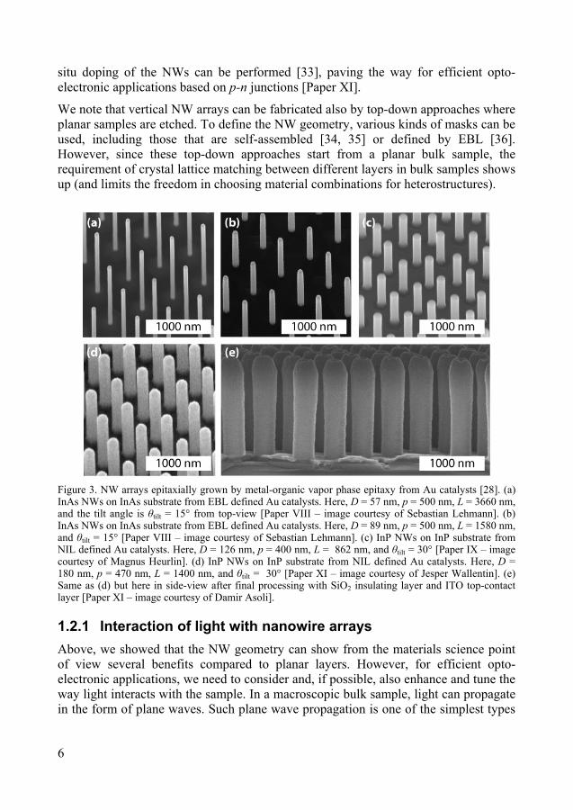
One of the common ways to initiate NW growth is to use Au catalyst particles [18, 26-28] [see Figure 3 for scanning electron microscopy (SEM) images of such fabricated NWs]. The Au catalyst particles and their positions (and consequently the position of the NWs) can be defined for example by electron beam lithography (EBL) or nano-imprint lithography (NIL) [27, 29, 30], or the particles can be deposited at random positions as aerosols [31]. By a proper choice of the crystallographic direction of the substrate, the NWs can be made to grow in the vertical direction [24, 27, 30]. When fabricated as an array, such vertical NWs can be packed tightly to enhance the output signal in NW based opto-electronic devices [6, 25, 27, 32, Paper XI]. Furthermore, in-
6
situ doping of the NWs can be performed [33], paving the way for efficient opto-electronic applications based on p-n junctions [Paper XI].
We note that vertical NW arrays can be fabricated also by top-down approaches where planar samples are etched. To define the NW geometry, various kinds of masks can be used, including those that are self-assembled [34, 35] or defined by EBL [36]. However, since these top-down approaches start from a planar bulk sample, the requirement of crystal lattice matching between different layers in bulk samples shows up (and limits the freedom in choosing material combinations for heterostructures).
Figure 3. NW arrays epitaxially grown by metal-organic vapor phase epitaxy from Au catalysts [28]. (a) InAs NWs on InAs substrate from EBL defined Au catalysts. Here, D = 57 nm, p = 500 nm, L = 3660 nm, and the tilt angle is θtilt = 15° from top-view [Paper VIII – image courtesy of Sebastian Lehmann]. (b) InAs NWs on InAs substrate from EBL defined Au catalysts. Here, D = 89 nm, p = 500 nm, L = 1580 nm, and θtilt = 15° [Paper VIII – image courtesy of Sebastian Lehmann]. (c) InP NWs on InP substrate from NIL defined Au catalysts. Here, D = 126 nm, p = 400 nm, L = 862 nm, and θtilt = 30° [Paper IX – image courtesy of Magnus Heurlin]. (d) InP NWs on InP substrate from NIL defined Au catalysts. Here, D = 180 nm, p = 470 nm, L = 1400 nm, and θtilt = 30° [Paper XI – image courtesy of Jesper Wallentin]. (e) Same as (d) but here in side-view after final processing with SiO2 insulating layer and ITO top-contact layer [Paper XI – image courtesy of Damir Asoli].
1.2.1 Interaction of light with nanowire arrays
Above, we showed that the NW geometry can show from the materials science point of view several benefits compared to planar layers. However, for efficient opto-electronic applications, we need to consider and, if possible, also enhance and tune the way light interacts with the sample. In a macroscopic bulk sample, light can propagate in the form of plane waves. Such plane wave propagation is one of the simplest types

7
of light propagation in optics and facilitates the analysis of the optical response considerably. In contrast, when a structure is tailored with features at the length scale of the wavelength of light, strongly modified and tunable propagation of light could be expected [37-40]. Thus, in the three-dimensional NW geometry, a more complicated type of light propagation could be expected.
We show in Figure 4 a schematic of a NW array of period p with NWs of diameter D and length L. Thus, we note here three independent geometrical parameters that could have separate effects on the optical response of the array. Furthermore, we denote often by f the fraction of the substrate surface that is covered by NWs. To simplify the terminology, we use in the following the terms NW area coverage and area coverage of NWs for this fraction.
In the schematic in Figure 4, light is incident at normal angle to the array, that is, the light propagates parallel to the NW axis. This incidence condition is of major interest for applications since it maximizes the area of the NW array projected to the incident light. Therefore, we concentrate on normally incident light in the following.
In the following chapters, we give an overview of how light interacts with vertical, absorbing NWs. After that, we end with presenting a selected set of applications where NW arrays and their nanophotonic properties are employed.
Figure 4. Schematic of a square array of vertical NWs of period p with NWs of diameter D and length L. Here, the light is incident at normal angle to the array (that is, the incident light propagates parallel to the axis of the NWs).

9
2 Measurement of optical properties of nanowire arrays
In many opto-electronic applications, it is of interest to experimentally assess the optical response of the NW arrays. Such optical response could for example be the fraction of incident light reflected or absorbed by the array [41], the emission pattern of photons originating from emitters placed within the array [42], or the photoluminescence response that involves both in- and out-coupling of light [43]. Here, we briefly review reflectance and absorptance measurements. These measurements are straight-forward to perform and yield, especially for photovoltaic and photodetection applications, very valuable information about the way light interacts with the NWs. Beyond these purely optical measurements, combined electro-optical measurements like external quantum efficiency (EQE) measurements for solar cells [1, Paper XI] and photoconductivity measurements for photodetectors [11, 25, Paper X] can be performed. Such combined measurements are described in more detail in Chapter 5.
2.1 Reflectance measurements The basic idea of reflectance measurements is quite simple: Light is sent in toward the sample and the amount of light coming back from the sample is measured. However, such measurements can be performed in varying ways. Therefore, we give below a brief summary of some of the most important technical details.
Before continuing, we clarify the terminology. Usually, it is possible to define a reference plane of the sample, as indicated in Figure 5. For example, if the sample contains a planar substrate, it is natural to take the top interface of that substrate as the reference plane. In this case, it is possible to define by an angle θinc the propagation direction of the incident light relative to the surface normal of that reference plane (see Figure 5). After this, it is possible to define the specular reflectance Rspec as the fraction of incident light that is reflected into a direction mirrored about the surface normal with respect to the incident direction (see Figure 5). Thus, also the specularly reflected light propagates at an angle θinc relative to the surface normal.
Of course, not all the light that is reflected has to end up in the specularly reflected beam. In principle, light can be scattered into an arbitrary angle θ (see Figure 5). If the reflectance over all scattering angles θ is collected, we obtain knowledge of the total reflectance R. After this, the diffuse reflectance Rdiff, which is the amount of light reflected outside the specular direction, can be calculated as Rdiff = R - Rspec.

10
Figure 5. Schematic of light incident toward a sample at an angle θinc with respect to the surface normal. The material of the sample has refractive index n2 whereas the top region has refractive index n1. The specularly reflected light is reflected into angle θinc (mirrored to the opposite side of the surface normal with respect to the direction of the incident light) and θ denotes an arbitrary angle into which light is reflected/scattered non-specularly. Here, θtr denotes the angle of propagation of the directly transmitted light. Note that n1sinθinc = n2sinθtr for non-absorbing materials according to Snell's law.
2.1.1 Specular reflectance
The specular reflectance of a NW array can be measured in principle by sending a collimated beam of light onto the sample and detecting the intensity of the specularly reflected beam. However, the diameter and length of NWs can vary over the sample, and the optical response of the array varies with these dimensions [Paper IX]. Thus, if the measurement spot size is too large, averaging effects can occur and valuable information about the local optical response could be lost.
A convenient way to limit the spot size is to do spatial filtering in an image plane of a focusing optics setup (such as a microscope) [36, Papers II, III, and VII-IX]. In that case, only light that originates from a limited part of the imaged surface is sent to the detector. Such spatial filtering could be performed for example by placing a limited-sized mirror or aperture in the image plane.
Since focusing optics is used in the spatial filtering, it is important to consider the effect of the numerical aperture (NA) of the objective lens on the measurements. Typically, the illumination by incident light and the collection of reflected light are performed with the same lens. The numerical aperture characterizes the range of propagation angles the lens can send light to and collect light from, i.e., the range of angles the lens can accept. The numerical aperture is defined as the sine of the largest angle the lens can accept (see Figure 6).
An increase of the NA has two distinct effects on reflectance measurements. First, light is incident from a larger variety of incidence angles. Thus, the measured reflectance averages over a larger fraction of the incidence angle dependence of the

11
optical response. Second, the amount of diffusively scattered light that is collected increases. Thus, when aiming to measure the specular reflectance, one should aim to use as low NA as possible since this collimates the incident light better and reduces at the same time the amount of diffusively reflected light that is collected (see Figure 6).
Figure 6. Schematic of the numerical aperture dependence on the shape of the illumination and collection cone for (a) NA = 0.5 and (b) NA = 0.13. With NA = 0.5 the half-angle of the cone is 30° whereas it is 7.5° for NA = 0.13.
Figure 7. Schematic of an integrating sphere where light enters the sphere through one view-port and illuminates the sample. The light reflected from the sample is scattered/reflected diffusively from the interior walls of the sphere. This randomizes the intensity on the interior surface of the sphere. A second view-port is used for extracting light to a detector. By making first a measurement on a reference sample of known reflectance, it is possible to calibrate the measurements to yield the reflectance of the sample.
12
2.1.2 Total reflectance
To measure the total reflectance R, a convenient way is to use an integrating sphere that is coated with a diffusively reflecting material on its interior surface [44, 45]. In such a sphere, light is typically sent onto the sample through a view-port of the sphere (see Figure 7). From the sample, light is reflected back into the sphere. When that reflected light reaches the interior surface of the sphere, it is scattered into a randomized direction due to the coating of the sphere. Next, that light is again scattered diffusively when reaching the surface of the sphere. After several such scattering events inside the sphere, the intensity of the light at the interior surface of the sphere is independent of position. Thus, no matter where a view-port for extraction of light to a detector is placed, the detected intensity Isample is the same (for a given size of the view-port).
To obtain the sample reflectance Rsample, the measurements need to be calibrated (we note that a very similar calibration procedure is applicable also when measuring the specular reflectance [Papers II, III, and VII-IX]). For this calibration, the background level Ibg needs to be measured. This is done without mounting a sample. Furthermore, a measurement of the reflected intensity Iref of a reference sample should be performed. The reference sample should have a well-known reflectance Rref. For this purpose, it is suitable to use for example a planar substrate for which the Fresnel equations yield Rref from tabulated values of the refractive index. After these measurements, the sample reflectance can be obtained through Rsample = Rref(Isample - Ibg)/(Iref - Ibg). This calibration takes thus into account the spectral variations in the intensity of the light source, in the sensitivity of the detector, and in the optical components of the optics system outside the sphere. Furthermore, stray-light that reaches the detector is taken into account by Ibg.
However, it should be noted that the spot size in an integrating sphere is typically on the order of a few millimeters [44]. Furthermore, spatial filtering in an image plane to limit the spot size, as described above, is not possible due to the working principle of the integrating sphere.
2.1.3 Dependence on the size of the measurement spot
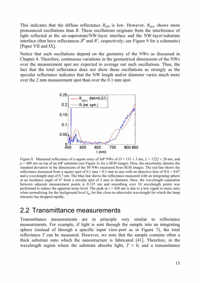
We show in Figure 8 the results of specular and total reflectance measurements on a NW array. The sample in this example consists of an InP NW array of p = 400 nm with NWs of D = 131 ± 3 nm and L = 1222 ± 20 nm (see Figure 3c for a SEM image and Figure 4 for a schematic). Here, the uncertainty denotes the standard deviation in the dimensions of 50 NWs measured at the middle of the spot for the specular reflectance measurement.
The total reflectance R is measured using a circular spot of 2 mm in diameter. In contrast, the specular reflectance Rspec is measured with NA = 0.13 from a square spot of 0.1 mm × 0.1 mm in size, located at the center of the much larger circular spot. In Figure 8, it is seen that both R and Rspec show very similar values and overall trends.
13
This indicates that the diffuse reflectance Rdiff is low. However, Rspec shows more pronounced oscillations than R. These oscillations originate from the interference of light reflected at the air-superstrate/NW-layer interface and the NW-layer/substrate interface (that have reflectances R0 and R1, respectively; see Figure 9 for a schematic) [Paper VII and IX].
Notice that such oscillations depend on the geometry of the NWs as discussed in Chapter 4. Therefore, continuous variations in the geometrical dimensions of the NWs over the measurement spot are expected to average out such oscillations. Thus, the fact that the total reflectance does not show these oscillations as strongly as the specular reflectance indicates that the NW length and/or diameter varies much more over the 2 mm measurement spot than over the 0.1 mm spot.
Figure 8. Measured reflectance of a square array of InP NWs of D = 131 ± 3 nm, L = 1222 ± 20 nm, and p = 400 nm on top of an InP substrate (see Figure 3c for a SEM image). Here, the uncertainty denotes the standard deviation in the dimensions of the 50 NWs measured from SEM images. The red line shows the reflectance measured from a square spot of 0.1 mm × 0.1 mm in size with an objective lens of NA = 0.07 and a wavelength step of 0.7 nm. The blue line shows the reflectance measured with an integrating sphere at an incidence angle of 8° from a circular spot of 2 mm in diameter. Here, the wavelength separation between adjacent measurement points is 0.335 nm and smoothing over 10 wavelength points was performed to reduce the apparent noise level. The peak at λ ≈ 420 nm is due to a low signal to noise ratio when normalizing for the background level Ibg for this close-to-ultraviolet wavelength for which the lamp intensity has dropped rapidly.
2.2 Transmittance measurements Transmittance measurements are in principle very similar to reflectance measurements. For example, if light is sent through the sample into an integrating sphere (instead of through a specific input view-port as in Figure 7), the total reflectance T can be measured. However, we note that the sample contains often a thick substrate onto which the nanostructure is fabricated [41]. Therefore, in the wavelength region where the substrate absorbs light, T ≈ 0, and a transmittance
14
measurement does not yield any additional information about the optical response of the nanostructures [41].
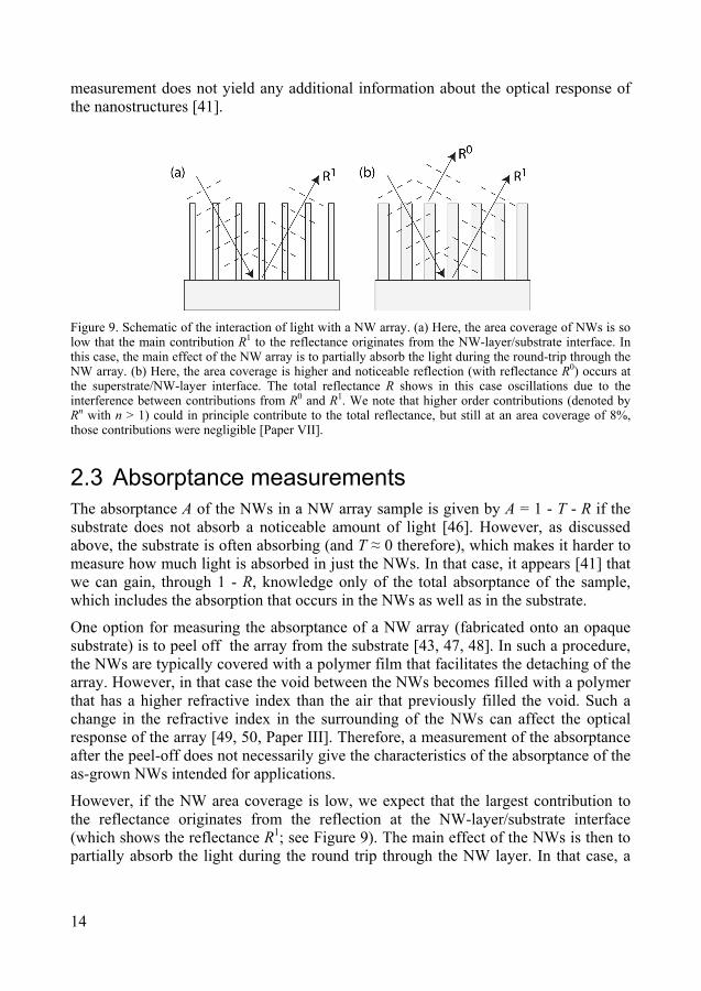
Figure 9. Schematic of the interaction of light with a NW array. (a) Here, the area coverage of NWs is so low that the main contribution R1 to the reflectance originates from the NW-layer/substrate interface. In this case, the main effect of the NW array is to partially absorb the light during the round-trip through the NW array. (b) Here, the area coverage is higher and noticeable reflection (with reflectance R0) occurs at the superstrate/NW-layer interface. The total reflectance R shows in this case oscillations due to the interference between contributions from R0 and R1. We note that higher order contributions (denoted by Rn with n > 1) could in principle contribute to the total reflectance, but still at an area coverage of 8%, those contributions were negligible [Paper VII].
2.3 Absorptance measurements The absorptance A of the NWs in a NW array sample is given by A = 1 - T - R if the substrate does not absorb a noticeable amount of light [46]. However, as discussed above, the substrate is often absorbing (and T ≈ 0 therefore), which makes it harder to measure how much light is absorbed in just the NWs. In that case, it appears [41] that we can gain, through 1 - R, knowledge only of the total absorptance of the sample, which includes the absorption that occurs in the NWs as well as in the substrate.
One option for measuring the absorptance of a NW array (fabricated onto an opaque substrate) is to peel off the array from the substrate [43, 47, 48]. In such a procedure, the NWs are typically covered with a polymer film that facilitates the detaching of the array. However, in that case the void between the NWs becomes filled with a polymer that has a higher refractive index than the air that previously filled the void. Such a change in the refractive index in the surrounding of the NWs can affect the optical response of the array [49, 50, Paper III]. Therefore, a measurement of the absorptance after the peel-off does not necessarily give the characteristics of the absorptance of the as-grown NWs intended for applications.
However, if the NW area coverage is low, we expect that the largest contribution to the reflectance originates from the reflection at the NW-layer/substrate interface (which shows the reflectance R1; see Figure 9). The main effect of the NWs is then to partially absorb the light during the round trip through the NW layer. In that case, a

15
reflectance measurement can be used for quantitatively extracting a value Aappr [Paper VII], which approximates A much better than 1- R (see Figure 10).
Figure 10. Modeled absorptance A and modeled 1 - R of an InAs NW array with p = 500 nm, D = 73 nm, and L = 1940 nm for normally incident light. Here, appr sub sub1 (1 ) /A R R R R is the refined approximation [Paper VII] for the absorptance. In this case, Rsub is the reflectance of a planar air/InAs interface for which the Fresnel equations with tabulated values [51] for the refractive index of InAs were used. The inset shows the modeled reflectance R and the calculated Rsub that are used for the calculation of Aappr. Notice that the reflectance of the sample differs considerably from that of the substrate, but due to considerable transmission into the substrate, 1 - R approximates the absorptance A of the NWs poorly. In contrast Aappr gives here an excellent approximation to A.


17
3 Modeling the optical response of nanowire arrays
To aid in the design of NW arrays for varying nanophotonic applications and to be able to theoretically analyze the results from optical measurements, the optical response of the NW arrays needs to be modeled. The NW array is a three-dimensional system (see Figures 3 and 4), and therefore several geometrical design parameters, such as the NW diameter and length as well as the array period, exist and could have separate, independent effects on the optical response. As will be detailed in this chapter, the appropriate modeling tools for describing the optical response depend on the geometrical dimensions of the NWs.
3.1 Geometrical optics Many of the light scattering properties of the macroscopic objects that surround us in everyday life can be described by geometrical optics [11]. In geometrical optics, light is described as rays with a well-defined propagation direction. The material properties are described by a refractive index n, and light travels with the speed c = c0/n in the medium.
A postulate of geometrical optics (Fermat's principle) states that light travels the fastest path between two points. From this postulate it follows that (i) rays follow a straight path in a bulk medium, and (ii) refraction occurs at the interface between two different materials (of refractive index n1 and n2) leading to a change in the propagation angle of the rays from θinc to θtr. This refraction is described by the Snell's law n1sin(θinc) = n2sin(θtr) [see Figure 5].
By tracing the paths of the rays originating from point-like sources, the image formation capability of optical systems such as microscopes and telescopes can be analyzed and designed [11]. Such ray tracing can be used also for studying the absorption in macroscopic samples if the absorption coefficient α of the material is included in the analysis [Paper IV]. In such an analysis, the light intensity is absorbed, that is, it decays, as exp(-αz) where z is the propagation direction of the ray inside the absorbing medium.
However, due to the ray-character of light in geometrical optics, effects that originate from the wave character of light are hard to include in the analysis. In nanostructures, features with size on the order of the wavelength of light exist. The interference of light-waves scattered from these features can dominate the optical response of the whole sample [Paper IV]. Thus, modeling tools beyond ray tracing are needed for appropriately describing the optical response of NW arrays.
18
3.2 Wave optics To be able to describe diffraction and interference of light, we use as a first step a scalar wavefunction u(r,t) to describe the light [11]. This wavefunction obeys the wave equation 2 2 2 2 2
0( , ) ( ) / ( , ) / 0u t n c u t t r r r . Thus, the geometry and materials of the light-scattering system are included in the wave equation through n(r).
As a specific solution for the wave equation, we consider monochromatic waves with a harmonic time dependence of the form u(r,t) = a(r)cos[ωt + φ(r)] where a(r) is the amplitude, ω the angular frequency, and φ(r) the phase. Due to the linear character of the wave equation, the superposition principle applies and the sum u1 + u2 of two wavefunctions u1 and u2 is also a solution to the wave equation. In this way, interference and diffraction effects can be taken into account by summing up the contributions un of light scattered from different parts of the system.
However, since in this wave optics description, light is described by a scalar wave function, polarization dependent phenomena cannot be resolved. Furthermore, the wave optics description does not yield the fraction of light scattered at an interface (especially since these are polarization dependent for non-normal incidence). For a NW, we could expect a noticeable scattering of light from the side walls of the NW due to the large surface to volume ratio typical for a NW. Thus, it could be expected that a more refined description than wave optics is needed for NW arrays.
3.3 Electromagnetic optics To describe the scattering of light when diffraction, interference, and polarization effects are of importance, we turn to electromagnetic optics. Here, the light is described as an electromagnetic field which consists of an electric part ( , )tE r and a magnetic part ( , )tH r [11, Paper VI]. The polarization of the light is included in the vector-character of the fields. We note that the polarization is defined often with reference to the orientation of the electric field [11]. Here, we consider monochromatic light and introduce the complex valued electric and magnetic fields
( )E r and ( ).H r These fields are connected to the real-valued, physical fields through the relations ( , ) Re ( ) exp( )t i t E r E r and ( , ) Re ( )exp( ) .t i t H r H r
In the following, we make the assumptions that the materials we consider are non-magnetic, linear, isotropic, and show a local optical response [Paper VI]. In this case, the Maxwell's equations are given by [Paper VI]
0( ) , ( )i H r r E r (1)
and
0( ) ( ).i E r H r (2)
Here, μ0 = 4π×10−7 V·s/(A·m) is the permeability of vacuum, ε(r,ω) = n(r,ω)2 is the dielectric function, and ε0 = 1/( μ0c0
2) ≈ 8.854187817×10⁻¹² F·m−1 is the permittivity of
19
vacuum. Absorption in the system is introduced by a non-zero (positive-valued) imaginary part of the refractive index n.
We note that in this electromagnetic description, the electromagnetic field is a continuous variable. Thus, electromagnetic optics does not include effects caused by the quantized nature of the photons that constitute the field. For the case of NWs, such effects can show up for example in the emission from a quantum dot in a NW [52]. Due to the quantized nature of the system, just one photon at a time can be emitted [52]. For an in-depth theoretical analysis of such effects, a quantum optics description is needed [11]. However, notice that at an intensity of 1 W/m2 of visible light, the flux of photons is on the order of 1018 photons per square meter and second. A typical value for solar irradiance is 1000 W/m2 [2]. We expect therefore that the quantization of the electromagnetic field at the level of single photons has only very minor effects at such intensities.
3.4 Choice of the optical description When choosing how to describe and analyze the optical response of NW arrays, the main choice is between geometrical optics and electromagnetic optics. Geometrical optics appears to be a good choice for describing the visible-light response of arrays where the diameter of the wires is in the micrometer range [53, 54] (notice that visible light has wavelengths in the approximate range of 400 to 700 nm). However, in many NW arrays, the diameter is on the order of the wavelength of light in the NW material [25, 32, 55]. In such a case, we could expect strong contributions from diffraction, interference, and polarization effects, which require electromagnetic optics for successful description.
3.5 Validity of the electromagnetic modeling We have previously shown that electromagnetic optics reproduces the measured reflectance spectra of NW arrays both before [Paper II] and after [Paper III] an Al2O3 coating layer is deposited on top of the NWs. Furthermore, the EQE of NW solar cells could be modeled accurately [Paper XI], and the electromagnetic optics works so well that geometrical dimensions of NWs can be extracted from measured reflectance spectra as described in Chapter 5.1 [56, Paper IX]. This very good agreement between measurements and modeling indicates a high validity of the electromagnetic modeling.
3.6 Numerical methods for electromagnetic optics For the three dimensional NW arrays (see Figure 3 for SEM images and Figure 4 for a schematic), the Maxwell's equations [Eqs. (1) and (2)] cannot be solved analytically. Instead, we must resort to numerical methods. In the field of computational electromagnetism, a large number of numerical methods exist for solving the

20
Maxwell's equations. For the numerical modeling of the optical response of the NW arrays, the three most common methods appear to be the finite element method (FEM) [57-60], the finite difference time domain method (FDTD) [36, 41, 45, 46, 61-64] and various methods closely related to the Fourier modal method (FMM) [65-69, Papers I-XI].
Figure 11. (a) Schematic of a system divided into slices suitable for the scattering matrix method [Paper VI]. Here, the system consists of three slices [that is, five slices including the substrate (slice 4) and superstrate (slice 0)]. In each slice, the geometry of the structure is invariant in the z direction. Here,
( )j C denotes the expansion coefficients of forward (+) and backward (-) propagating eigenmodes in the
jth slice. (b) Schematic of an array of Al2O3 coated InAs NWs [Paper III]. The optical response of this array can be modeled by the scattering matrix method using three slices as schematically depicted in (a). Note that in this case 4
C 0 since no light is incident from the InAs substrate, and 0C describes the
light incident from the top side.
3.6.1 Fourier modal method
The Fourier modal method (FMM) [70-73] is a computational method where a complete basis of eigenmodes [74] is used for expanding the electromagnetic field in the different slices of a layered system (see Figures 11a and 11b for a schematic). A typical NW array consists of a very limited number of such slices (see Figure 11). Thus, the FMM appears to be suitable for the analysis of these structures. Therefore, we give some of the main details of the method below.
To obtain the eigenmodes used in the FMM, a Fourier basis is used first for expanding the electromagnetic field [70-73]. By limiting the number of components used in the Fourier basis, that is, by truncating the basis, an eigenvalue problem for the eigenmodes is obtained in a matrix form suitable for calculations [Paper VI].
We note that a way for enhancing the convergence rate (and therefore the computational time) of the FMM was discovered by Li [75]. In that seminal work, it was shown how the truncated Fourier expansion of a product of pair-wise

21
discontinuous functions can be made to converge faster. Those results were of direct importance for the FMM since the component of εE normal to an interface is continuous [11, 75] (thus, ε and the normal component of E are pair-wise discontinuous at the interface between materials of dissimilar ε). A generalization of the work by Li on two-dimensional systems was performed by Popov and Nevière for arbitrary shaped structures [76], which enhanced the convergence rate in the modeling of three-dimensional systems.
An implementation of the FMM can be summarized as follows [Paper VI]:
1) We single out the z direction as the direction of light propagation (see Figure 11a).
2) The light scattering system is divided into n slices in the z direction such that the dielectric function is invariant in the z direction in each slice (see Figure 11).
3) Next, a Fourier basis is used for expanding the electromagnetic field. This yields for each slice an eigenvalue problem. That eigenvalue problem has the optical eigenmodes of the slice as solutions, with corresponding eigenvalues β. These eigenmodes show, due to the invariance of ε in the z direction, a simple type of propagation of the form exp(±iβz) in the z direction. Thus, the eigenmodes propagate (or grow exponentially) either in the forward (+) or the backward (-) direction [Paper VI]. (Notice that we choose Imβ > 0 if Imβ ≠ 0.)
4) In each slice, the total electromagnetic field is expanded in the eigenmodes obtained in (3) above. We use j
C and jC to denote the expansion
coefficients of the forward (+) and backward (-) propagating eigenmodes in the jth slice.
5) The electromagnetic field of the incident light is projected onto the optical eigenmodes of the superstrate and substrate. This step fixes 0
C and 1nC that
describe, respectively, the light that is incident from the superstrate (slice 0) and the substrate (slice n+1).
6) To connect the expansion coefficients of the eigenmodes in neighboring slices, we use the condition that the transverse (that is, the x and y) components of the E and H fields should be continuous at the interface between the slices.
7) Finally, we propagate the electromagnetic field through each slice. This gives a set of linear equations [77], whose solution yields the expansion coefficients
jC and j
C in all slices and therefore the solution to the light scattering problem. Instead of working with that linear equation system explicitly, a convenient alternative is to use matrix algebra as described below.

22
Figure 12. (a) Computational time of the scattering matrix method for increasing size of the truncated basis, whose size is given here in terms of M [note that the number of basis functions in the two dimensional Fourier basis used for expanding the eigenmodes is (2M +1)2] [Paper VI]. These simulations were performed on a single CPU core of a 3.40GHz Intel Pentium D processor. Here, normally incident light for a square array was modeled and reduction of the basis size was used, which speeds up the calculation by up to a factor of 64 for normally incident light (due to the C4v symmetry) [78]. Due to the reduction of the basis size, the matrix size in the calculations is N = (M+1)2+M2. For M > 20, we find a dependence of N2.87 on the computational time. b) Modeled absorptance of a square array of InP NWs of (i) D = 180 nm, p = 400 nm, and L = 2000 nm; and (ii) D = 62 nm, p = 500 nm, and L = 1444 nm on top of an InP substrate. The light is incident from the top air side at normal angle and there is air also between the NWs. (c) Same as (b) but here A for M = 40 is taken as a reference level and |A(M) - A(M = 40)| is shown instead.
23
3.6.1.1 Scattering matrix method
For the propagation and matching of the eigenmodes inside the scattering system in the FMM, a particularly convenient method is to use the scattering matrices presented in [79-82, Paper VI]. The use of these matrices has two main benefits: (1) The boundary condition for the light scattering problem is fixed by the incident light, which is the natural boundary condition for many light scattering problems, and (2) the propagation inside the system is formulated such that exponentially growing eigenmodes do not show up explicitly in the numerical implementation. Point (2) has the very important implication that the method is numerically stable. This is in contrast to methods where a transfer matrix is used for propagating the field through each slice [79], since there the growing eigenmodes show up and could cause problems with arithmetic overflow during the computation.
In the scattering matrix method, a scattering matrix S is used for describing the optical response of the system [79-82, Paper VI]. For a system consisting of n slices (see Figure 11a), the light scattered by the system is given by
T T
1 0 0 1, ,n n C C S C C .
From 0C and 1n
C , the reflectance and transmittance of the system can be calculated
[Paper VI]. Furthermore, with the scattering matrix method, the electromagnetic field distributions inside the structure can be readily calculated. From these distributions, the power flow inside the structure can be calculated [Paper V]. Furthermore, from the eigenmode expansion inside the structure, it is possible to analyze in detail which of the eigenmodes contribute to the power transport and absorption/dissipation inside the system [74, Paper V].
3.6.1.2 Computational time and convergence rate
We show in Figure 12 the computational time and convergence rate of the modeled absorptance of two NW arrays of D = 180 nm, p = 400 nm, and L = 2000 nm; and D = 62 nm, p = 500 nm, L = 1444 nm. We notice first that the convergence rate is noticeably slower for the array with the smaller diameter NWs. However, for both arrays, an accuracy better than 1 % (absolute) is reached with less than one second computational time (on a single core of a Intel Pentium D, 3.40GHz processor).
It should be noted that the computational time of the FMM is expected to scale as V3 with system volume V (the computational time scales as N3 for a large matrix size N [80, 83] and we assume that N is proportional to V). For example, let us assume that we shift from the square array in Figure 12 to an array with a supercell that contains four NWs that break the symmetry of the system. Then, the expected increase in computational time is more than a factor of 4000 (or more exactly: a factor of 64×64, where the first factor arises from the increase by a factor of 4 of the unit cell volume V, and the second factor arises from the breaking of the symmetry). Therefore, for simulations with large super-cells containing many NWs, for example FDTD, for which the computational time scales linearly with V [84] could be a suitable option to reduce the numerical burden [62].


25
4 Optical properties of absorbing nanowire arrays
The optical response of absorbing NW arrays is determined to a large extent by the relation between the NW diameter D and the wavelength λ of the light, as detailed in this chapter. To summarize, when D >> λ, the interaction of light with the NWs can be described by geometrical optics. In the opposite limit case, when D << λ, the interaction can be described by electrostatics. However, when D ≈ λ, we enter instead the regime of nanophotonics where optical resonances can show up [36, 85, Paper IV]. These resonances can be used for tuning strongly the absorption in the NW arrays.
4.1 Geometrical optics limit We have shown that the optical response of the NWs can be described satisfactorily by geometrical optics when the diameter of the NWs is considerably larger than the wavelength of light [Paper IV]. For normally incident light, only light rays that are incident toward the top cross-section of a NW can interact with the NW (see Figure 13). The incoupling reflection loss of these interacting rays is given by the reflectance Rin = |1 - nNW|2/|1 + nNW|2 of a planar interface. Here, nNW is the refractive index of the NW material. Next, the absorptance ANW of the light coupled into the NWs of length L is given by the Beer-Lambert law: ANW = 1 - exp(-αbulkL). Here, αbulk = 4πIm(nNW)/λ is the bulk absorption coefficient of the NW material. Therefore, the absorptance of a NW array of NW area coverage f = π(D/2)2/p2 is given by A = ANW(1-Rin)f [Paper IV].
Figure 13. Schematic of the interaction of normally incident light with a NW array in the geometrical optics limit of D >> λ. Light rays that are incident toward the top of a NW are partially reflected back to the air superstrate and partially transmitted into the NW according to the Fresnel equations. Inside the NW, the transmitted rays decay similarly as in a bulk sample. In contrast, the rays that travel between the NWs continue to the substrate interface without interacting with the NWs.

26
Thus, in this geometrical optics limit, the NWs absorb light similarly as a bulk sample. However, the limited NW area coverage f and the insertion reflection loss Rin restrict the amount of light that can couple into the NWs. To reduce Rin, it is in principle possible to apply thin film coating techniques developed for planar samples [53]. Furthermore, to reduce the limitation in absorption performance due to the limited NW area coverage, it is possible to use for example dielectric particles between the NWs for scattering light into the NWs. However, NWs with D >> λ are not of central interest for this introduction since the possibility of combining lattice mismatched materials (as described in Chapter 1.2) is expected to disappear in these bulk-like structures. Furthermore, as shown below, NWs can show novel nanophotonic response when λ ≈ D, which merits concentrated studies separate from those on microwires.
4.2 Electrostatic limit The optical response of individual, horizontal NWs has been modeled successfully with electrostatics when the diameter of the NWs was much smaller than the wavelength of light [86]. The electrostatic analysis allowed for an analytical solution and showed how the high refractive index of the NWs can screen off the incident light from the NWs. We note that such electrostatic considerations have not been applied widely for arrays of vertical NWs.
However, we used recently an electrostatic approximation for studying the absorptance of vertical NW arrays when D << λ [Paper IV]. There, we derived an analytical expression Aestat for the absorptance by assuming that f << 1. From those results, it can be shown that the NW array can be replaced with a bulk layer of refractive index effn with Im( )effn / (4 )eff 2 2Im( )4Re( )/ | 1 |NW NW NWf n n n . Notice that Re( ) 1effn due to the assumption of f << 1. Hence, the absorption per volume material in the NWs is reduced, due to the electrostatic screening, by the factor of 2 2Im( ) / Im( ) 4Re( )/ | 1|eff NW NW NWn n f n n [Paper IV] (notice that we have here taken into account, by including f, the reduced amount of absorbing material in the NW array). Thus, to yield the same absorptance in the NWs as in a thin film of thickness t, the NWs need to have a length of L = t/(fη).
For many semiconductors, a typical value for the (real part of the) refractive index is in the proximity of 3.5 in the visible wavelength range (see Figure 15a). This value yields η ≈ 1/12, assuming that the imaginary part of the refractive index is considerably lower than the real part. As an example for absorption in a thin film, t ≈ 1 μm yields for InP an absorptance of 96 % when the photon energy is 0.2 eV above the band gap energy of 1.34 eV (that is, the absorbed photons are of 805 nm in wavelength). Assuming a NW area coverage of f = 10 %, the NWs in the electrostatic limit need to be more than 100 μm long for the NW array to yield an equal absorptance as the thin film with t = 1 μm. Such NW lengths are impractical already from a mechanical point of view due to sticking of adjacent NWs in dense arrays of high aspect-ratio NWs [87].

27
4.2.1 Effective medium theory
In principle, it is possible to refine the calculation of eff effn beyond that of the electrostatic approximation above. In the long wavelength limit, when λ >> D, p, an expression for eff can be obtained assuming a dipolar type of coupling between the NWs [88]. For light normally incident onto a NW array (see Figure 4 for a schematic), the electric field of the incident light is polarized perpendicular to the NW axis. For this case, [ 1 ( 1)] / [ 1 ( 1)]eff NW NW NW NWf f [88]. Notice that the optical response of the NW array is then equal to that of a substrate coated with a thin film of refractive index effn and thickness L, which simplifies the calculations considerably.
4.2.2 Absorptance in the electrostatic limit
We show in Figure 14a the calculated absorptance of a NW array with NWs of D = 10 nm when varying the NW area coverage f (by varying the period p of the array). Here, we compare the results obtained with the electrostatic approximation (Aestat) [Paper IV], the effective medium theory (AEMT) [88], and the full three dimensional electromagnetic modeling (A) [Paper VI]. We find that all three methods yield up to f = 0.1 very similar values for the absorptance. For f > 0.1, Aestat is smaller than AEMT and A. Since the absorption coefficient of the effective medium is given by
4 Im( ) /eff effn , this difference between Aestat and AEMT for f > 0.1 shows up also as Im(nEMT) > Im(nestat) for f > 0.1 (Figure 14c).
To understand why Aestat < A for f > 0.1, we turn to consider some of the details of the electrostatic approximation. For these small-diameter NWs, the electric field strength |E| inside the NWs is in the electrostatic limit a factor of 22/ | 1| 0.15NWn weaker than in the void between the NWs, due to the electrostatic screening [Paper IV]. Note that the intensity is expected to be proportional to the electric field strength squared [Paper IV]. Therefore, most of the intensity is carried in the void between the NWs. Thus, we expect that the increase in f increases the electric field strength in the void between the NWs to keep the integrated intensity constant (assuming that all the incident intensity is coupled into the NW array; the NW array shows low insertion reflection losses as discussed below). Such an increase of the electric field strength in the void is in turn expected to increase the electric field strength inside the absorbing NWs, and hence also the absorptance. In the electrostatic approximation, such an enhancement effect of the absorptance is however not taken into account (since f << 1 is assumed). Furthermore, increasing coupling between adjacent NWs with increasing f could further enhance the absorptance beyond that of Aestat.
When f > 0.6, A > AEMT (see Figure 14a). This discrepancy could originate from the fact that the calculation of AEMT takes into account only dipolar terms in the interaction between NWs [88]. Therefore, when the NWs are close to each other (i.e., when f is large) multipolar terms could enhance the interaction between NWs (and therefore the electric field strength inside the NWs), giving rise to an enhancement of A beyond that of AEMT.
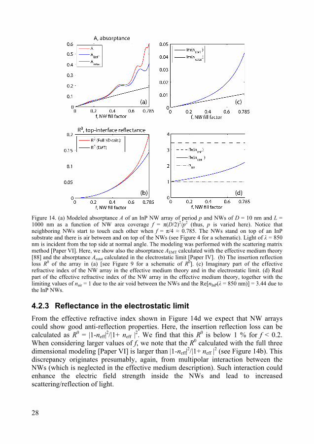
28
Figure 14. (a) Modeled absorptance A of an InP NW array of period p and NWs of D = 10 nm and L = 1000 nm as a function of NW area coverage f = π(D/2)2/p2 (thus, p is varied here). Notice that neighboring NWs start to touch each other when f = π/4 ≈ 0.785. The NWs stand on top of an InP substrate and there is air between and on top of the NWs (see Figure 4 for a schematic). Light of λ = 850 nm is incident from the top side at normal angle. The modeling was performed with the scattering matrix method [Paper VI]. Here, we show also the absorptance AEMT calculated with the effective medium theory [88] and the absorptance Aestat calculated in the electrostatic limit [Paper IV]. (b) The insertion reflection loss R0 of the array in (a) [see Figure 9 for a schematic of R0]. (c) Imaginary part of the effective refractive index of the NW array in the effective medium theory and in the electrostatic limit. (d) Real part of the effective refractive index of the NW array in the effective medium theory, together with the limiting values of nair = 1 due to the air void between the NWs and the Re[nInP(λ = 850 nm)] = 3.44 due to the InP NWs.
4.2.3 Reflectance in the electrostatic limit
From the effective refractive index shown in Figure 14d we expect that NW arrays could show good anti-reflection properties. Here, the insertion reflection loss can be calculated as R0 = |1-neff|
2/|1+ neff |2. We find that this R0 is below 1 % for f < 0.2. When considering larger values of f, we note that the R0 calculated with the full three dimensional modeling [Paper VI] is larger than |1-neff|
2/|1+ neff |2 (see Figure 14b). This
discrepancy originates presumably, again, from multipolar interaction between the NWs (which is neglected in the effective medium description). Such interaction could enhance the electric field strength inside the NWs and lead to increased scattering/reflection of light.

29
4.2.4 Enhanced absorption by dielectric shell
For applications based on absorption of light in small-diameter NWs, approaches for decreasing the electrostatic screening are desired. An intuitive approach, inspired by thin-film anti-reflection coatings, is to try to coat the NWs with a material of refractive index between that of the NW material and the air surrounding the NWs. Indeed, we showed that by filling the space between the NWs with a material of refractive index 1.76 (corresponding to Al2O3 at a wavelength of 850 nm), the absorptance of the NWs increased by a factor of two [Paper III]. Such an increase was in line with an electrostatic analysis of core-shell cylinders [Paper III]. We note that similar dielectric coating techniques are proposed also for horizontal NWs for tuning the absorption [89].
4.3 Nanophotonic response of nanowire arrays First, we note that many of the NW arrays considered in recent literature have NWs placed in a two-dimensional, periodic lattice [59, 60, 64, 68, 69 Papers I-V and VII-XI]. Furthermore, in the nanophotonic regime where λ ≈ D, we could expect coherent scattering of light inside the NWs, and also between the NWs if λ ≈ p. Therefore, such a NW array resembles a two-dimensional photonic crystal [37] (note that a photonic crystal is characterized by a periodic modulation of the refractive index). It is well known that a photonic crystal shows a band structure for the optical eigenmodes [37, 38], similar to that for electrons in solid state crystals [4]. The research of photonic crystals is vast, but a knowledge transfer to the case of absorbing NW arrays is however not straight-forward since:
1) In photonic crystal research a common way to tune the optical response is to scale the geometrical dimensions by r → ar. Such scaling causes a frequency shift of ω → ω/a in the band structure of the photonic crystals [38]. For this simple tuning to apply, the refractive indices of the materials in the photonic crystal should not show dispersion (i.e., they should have the same values at ω and ω/a). However, in the region where a semiconductors absorbs light, we find often noticeable dispersion in n(ω), especially in Im[n(ω)] (see Figure 15b). Furthermore, the absorption coefficient at a given frequency can vary strongly between semiconductor materials (see Figure 15b for a comparison between InP and Si). Therefore, a specific study for each material system and each configuration of the array geometry is in principle needed (unless generally applicable guidelines are identified for the design of the NW arrays; see [Paper V] and Chapter 4.3.5).
2) The light is often incident along a direction parallel to the NW axis (see Figure 4 for a schematic). The two-dimensional photonic crystal lacks periodicity in this direction, and photonic band gaps do not open up. It appears
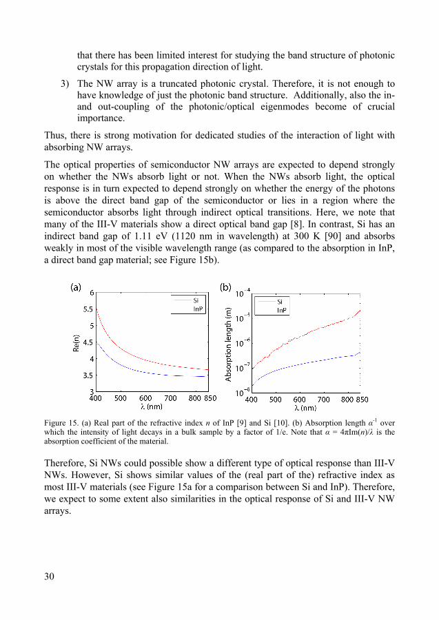
30
that there has been limited interest for studying the band structure of photonic crystals for this propagation direction of light.
3) The NW array is a truncated photonic crystal. Therefore, it is not enough to have knowledge of just the photonic band structure. Additionally, also the in- and out-coupling of the photonic/optical eigenmodes become of crucial importance.
Thus, there is strong motivation for dedicated studies of the interaction of light with absorbing NW arrays.
The optical properties of semiconductor NW arrays are expected to depend strongly on whether the NWs absorb light or not. When the NWs absorb light, the optical response is in turn expected to depend strongly on whether the energy of the photons is above the direct band gap of the semiconductor or lies in a region where the semiconductor absorbs light through indirect optical transitions. Here, we note that many of the III-V materials show a direct optical band gap [8]. In contrast, Si has an indirect band gap of 1.11 eV (1120 nm in wavelength) at 300 K [90] and absorbs weakly in most of the visible wavelength range (as compared to the absorption in InP, a direct band gap material; see Figure 15b).
Figure 15. (a) Real part of the refractive index n of InP [9] and Si [10]. (b) Absorption length α-1 over which the intensity of light decays in a bulk sample by a factor of 1/e. Note that α = 4πIm(n)/λ is the absorption coefficient of the material.
Therefore, Si NWs could possible show a different type of optical response than III-V NWs. However, Si shows similar values of the (real part of the) refractive index as most III-V materials (see Figure 15a for a comparison between Si and InP). Therefore, we expect to some extent also similarities in the optical response of Si and III-V NW arrays.
31
4.3.1 Silicon nanowire arrays
The research of the optical properties of Si NW arrays is broad, motivated by the abundance of Si, which makes it an economically important semiconductor for opto-electronics [25]. Below, we highlight very briefly some of the aspects we find most important for understanding the absorption of light in Si NW arrays, especially for photovoltaics.
In the seminal modeling study by Hu and Chen [91], the optical properties of vertical Si NW arrays were studied for the case in which the array period p was less than 100 nm. It was discovered that NW arrays can exhibit excellent antireflection properties in the sense that the free-standing (that is, substrate-free) array reflected much less light than a planar Si substrate. Furthermore, the NWs absorbed short-wavelength light more efficiently than a corresponding thin film, and absorption of long wavelength light could be enhanced by increasing the NW area coverage f.
Later, Lin and Povinelli [68] relaxed in their theoretical study the limit on the period. The study showed that a Si NW array of 600 nm in period and NWs of 540 nm in diameter gave an optimized absorption of sunlight, which was 72% better than that of a planar reference sample. The enhancement was ascribed partly to the excitation of guided modes in the in-plane direction within the NW array, that is, in the x-y plane of Figure 11.
4.3.2 Direct band-gap III-V nanowire arrays
For InP NWs with a length of L = 2000 nm, a NW diameter of D = 180 nm and an array period of p = 400 nm was indicated to give efficient absorption of sun light [Paper I]. These values were later refined to D = 180 nm and p = 360 nm [59]. Thus, neither too sparse nor too dense NW arrays were optimal for the absorption. The origin of this recommendation for a fairly large diameter can be derived partly to the fact that small-diameter NWs are close to the electrostatic limit described above (Chapter 4.2.2), where the absorption per volume semiconductor material is decreased considerably (by approximately a factor of 10 for typical semiconductors) due to the electrostatic screening [Paper IV]. Similar values of D ≈ 180 nm were proposed also for GaAs NWs [64].
An initial optimization study of p and D for varying L for III-V materials [69] showed that the (optimized) value of D/p decreased with increasing NW length. However, no general trends were found for how p varied with L, and no specific values for D were proposed. The decreasing value of D/p was ascribed to decreasing insertion reflection loss R0 with decreasing NW area coverage. Later, a study showed that there exist specific, band-gap dependent, diameters that are the most appropriate for the absorption of sun light, independent of the NW length [Paper V]. These diameters originate from optical resonances in the individual NWs of the array, as discussed in Chapter 4.3.5.

32
4.3.3 Comparison between silicon and III-V nanowire arrays
To highlight some of the similarities and differences between Si and direct band-gap III-V NW arrays, we show in Figure 16 modeled optical spectra (reflectance, transmittance, and absorptance) of Si and InP NW arrays. In this example, the geometry of the NW arrays is fixed to D = 160 nm, p = 300 nm, and L = 1000 nm. This yields a NW area coverage of f ≈ 22.3 %. Thus, the amount of material in the NWs is equal to that in a thin film of thickness t = fL = 223 nm in thickness. We show in Figure 16 also the absorptance of such a thin film (dashed line).
Figure 16. (a) Schematic of a NW array. (b) and (c) Modeled absorptance A, transmittance T and reflectance R of a square array of Si (b) and InP (c) NWs of p = 300 nm, D = 160 nm, and L = 1000 nm on a substrate of the same material as the NWs with air on top and between the NWs [see (a) for a schematic]. The modeling was performed for normally incident light with the scattering matrix method [Paper VI]. Here, we show also the absorptance of a thin film (dashed red line) that contains the same amount of absorbing material as the NW array [that is, the thickness of the thin film is t = Lf = Lπ(D/2)2/p2 = 223 nm]. For this thin film, we assumed a perfect anti-reflection coating on both the top and the bottom interface. Thus, no reflection of light occurs at these interfaces, and the absorptance of the thin film is therefore given by Atf = 1 - exp(-αbulkt).
First, we find that both the Si and the InP NW array absorb long wavelength light more efficiently than the corresponding thin film. Next, we notice that the absorptance of the InP NWs is considerably higher than that of the Si NWs for λ > 500 nm. This difference is understood from the much larger absorption coefficient in bulk InP than in bulk Si at the longest wavelengths considered in Figure 16 (see Figure 15b for the absorption length in InP and Si).
Regarding the reflectance of the arrays (Figure 16), we notice that the Si NW array shows stronger oscillation in R than the InP NW array. To understand this difference, we show in Figure 17 the R0, the insertion reflection loss at the top interface of the NW layer (see Figure 9 for a schematic). Both the Si and the InP NWs show similar values of R0 on the order of 0.05, which are much lower than the reflectance of above 30 % of the corresponding bare substrates (also shown in Figure 17). Thus, also in this nanophotonic regime, the NWs show good antireflection properties, similarly as in the
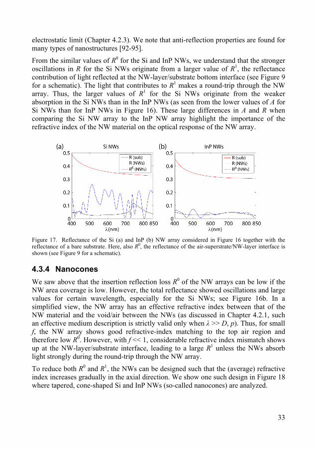
33
electrostatic limit (Chapter 4.2.3). We note that anti-reflection properties are found for many types of nanostructures [92-95].
From the similar values of R0 for the Si and InP NWs, we understand that the stronger oscillations in R for the Si NWs originate from a larger value of R1, the reflectance contribution of light reflected at the NW-layer/substrate bottom interface (see Figure 9 for a schematic). The light that contributes to R1 makes a round-trip through the NW array. Thus, the larger values of R1 for the Si NWs originate from the weaker absorption in the Si NWs than in the InP NWs (as seen from the lower values of A for Si NWs than for InP NWs in Figure 16). These large differences in A and R when comparing the Si NW array to the InP NW array highlight the importance of the refractive index of the NW material on the optical response of the NW array.
Figure 17. Reflectance of the Si (a) and InP (b) NW array considered in Figure 16 together with the reflectance of a bare substrate. Here, also R0, the reflectance of the air-superstrate/NW-layer interface is shown (see Figure 9 for a schematic).
4.3.4 Nanocones
We saw above that the insertion reflection loss R0 of the NW arrays can be low if the NW area coverage is low. However, the total reflectance showed oscillations and large values for certain wavelength, especially for the Si NWs; see Figure 16b. In a simplified view, the NW array has an effective refractive index between that of the NW material and the void/air between the NWs (as discussed in Chapter 4.2.1, such an effective medium description is strictly valid only when λ >> D, p). Thus, for small f, the NW array shows good refractive-index matching to the top air region and therefore low R0. However, with f << 1, considerable refractive index mismatch shows up at the NW-layer/substrate interface, leading to a large R1 unless the NWs absorb light strongly during the round-trip through the NW array.
To reduce both R0 and R1, the NWs can be designed such that the (average) refractive index increases gradually in the axial direction. We show one such design in Figure 18 where tapered, cone-shaped Si and InP NWs (so-called nanocones) are analyzed.
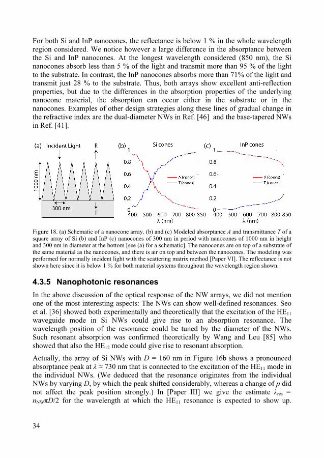
34
For both Si and InP nanocones, the reflectance is below 1 % in the whole wavelength region considered. We notice however a large difference in the absorptance between the Si and InP nanocones. At the longest wavelength considered (850 nm), the Si nanocones absorb less than 5 % of the light and transmit more than 95 % of the light to the substrate. In contrast, the InP nanocones absorbs more than 71% of the light and transmit just 28 % to the substrate. Thus, both arrays show excellent anti-reflection properties, but due to the differences in the absorption properties of the underlying nanocone material, the absorption can occur either in the substrate or in the nanocones. Examples of other design strategies along these lines of gradual change in the refractive index are the dual-diameter NWs in Ref. [46] and the base-tapered NWs in Ref. [41].
Figure 18. (a) Schematic of a nanocone array. (b) and (c) Modeled absorptance A and transmittance T of a square array of Si (b) and InP (c) nanocones of 300 nm in period with nanocones of 1000 nm in height and 300 nm in diameter at the bottom [see (a) for a schematic]. The nanocones are on top of a substrate of the same material as the nanocones, and there is air on top and between the nanocones. The modeling was performed for normally incident light with the scattering matrix method [Paper VI]. The reflectance is not shown here since it is below 1 % for both material systems throughout the wavelength region shown.
4.3.5 Nanophotonic resonances
In the above discussion of the optical response of the NW arrays, we did not mention one of the most interesting aspects: The NWs can show well-defined resonances. Seo et al. [36] showed both experimentally and theoretically that the excitation of the HE11 waveguide mode in Si NWs could give rise to an absorption resonance. The wavelength position of the resonance could be tuned by the diameter of the NWs. Such resonant absorption was confirmed theoretically by Wang and Leu [85] who showed that also the HE12 mode could give rise to resonant absorption.
Actually, the array of Si NWs with D = 160 nm in Figure 16b shows a pronounced absorptance peak at λ ≈ 730 nm that is connected to the excitation of the HE11 mode in the individual NWs. (We deduced that the resonance originates from the individual NWs by varying D, by which the peak shifted considerably, whereas a change of p did not affect the peak position strongly.) In [Paper III] we give the estimate λres = nNWπD/2 for the wavelength at which the HE11 resonance is expected to show up.

35
From this relation, we find that the Si NWs of 160 nm in diameter are expected to show a resonance at λres ≈ 820 nm, in good agreement with the position of the absorptance peak at λ ≈ 730 nm. Similarly, the InP NW array shows a pronounced dip of the transmittance at λ ≈ 690 nm, which corresponds to strong absorption in the NWs due to the resonant excitation of the HE11 mode. This 5 % difference in the resonance wavelength between the InP NWs and the Si NWs is in line with the 10 % difference between the real part of the refractive index of InP and Si (see Figure 15).
To study the optical resonance in more detail, we note that the local absorption in the NWs is proportional to Im(εNW)|E|2 [Paper IV]. Thus, by varying Re(εNW) while keeping Im(εNW) constant, we can use the absorptance spectrum for studying how the resonance affects the average electric field strength inside the NWs [note that A is proportional to Im(εNW)<ENW
2> where <ENW2> is the average of the electric field
strength squared in a NW].
Figure 19. Modeled absorptance at λ = 700 nm of a NW array with p = 600 nm, D = 142 nm, and L = 1000 nm (see Figure 16a for a schematic) as a function of Re(εNW), the real part of the dielectric function of the NW material [note that εNW = (nNW)2]. Here, Im(εNW) = 1.83, the value of Im(εInP) at λ = 700 nm. Notice that the resonance occurs at Re(εNW) = 12.1, the value of Re(εInP) at λ = 700 nm.
We show in Figure 19 the modeled absorptance of an array of NWs with D = 142 nm. Here, Re(εNW) is varied for λ = 700 nm, and Im(εNW) is fixed to the value of 1.83 that corresponds to that of InP at λ = 700 nm. Thus, since Im(εNW) is fixed, the absorptance spectrum yields direct information about <ENW
2>. When Re(εNW) ≈ 12.1, which is the value for InP at λ = 700 nm, the absorptance shows a peak of 0.98 due to resonant excitation of the HE11 mode. In contrast, at both Re(εNW) = 4 and 20, the absorptance shows considerably lower values of less than 0.4. Thus, we expect a much stronger electric field strength inside the NWs for Re(εNW) ≈ 12.1 than for Re(εNW) = 4 and 20.
We show in Figure 20 the electric field distributions at Re(εNW) = 4, 12.1, and 20. For Re(εNW) = 12.1, we observe the resonant excitation of the HE11 mode which leads to a large electric field strength inside the NWs. Here, almost no light reaches the
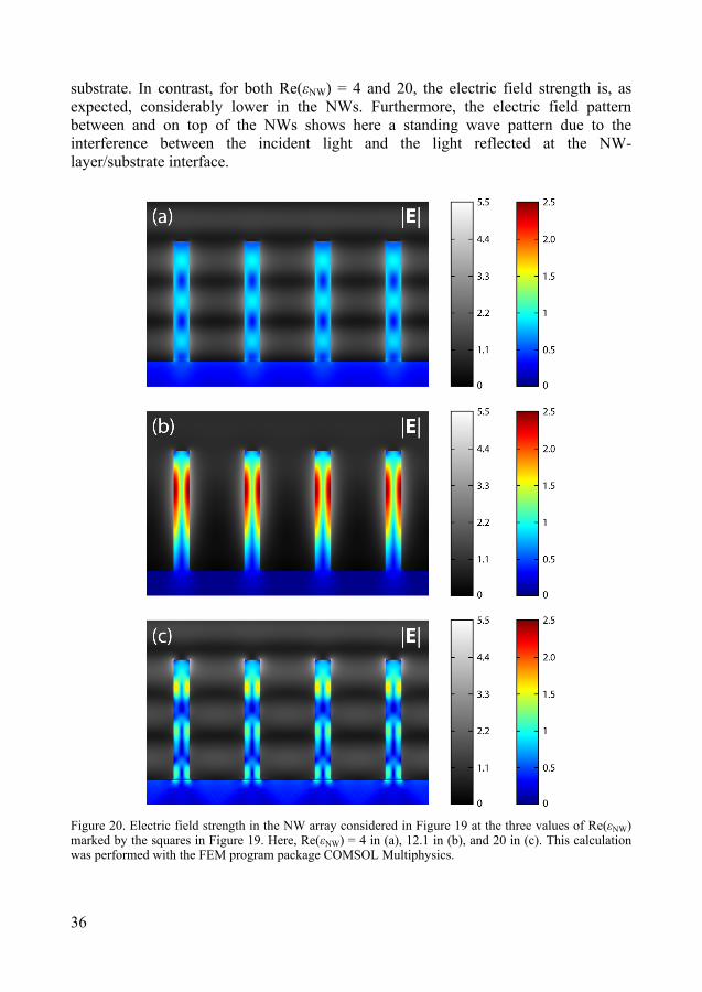
36
substrate. In contrast, for both Re(εNW) = 4 and 20, the electric field strength is, as expected, considerably lower in the NWs. Furthermore, the electric field pattern between and on top of the NWs shows here a standing wave pattern due to the interference between the incident light and the light reflected at the NW-layer/substrate interface.
Figure 20. Electric field strength in the NW array considered in Figure 19 at the three values of Re(εNW) marked by the squares in Figure 19. Here, Re(εNW) = 4 in (a), 12.1 in (b), and 20 in (c). This calculation was performed with the FEM program package COMSOL Multiphysics.

37
Thus, the NWs can show diameter-tunable absorption resonances [85, Papers IV, V, and X]. We have shown that such resonances can enhance the absorption per volume semiconductor material by a factor of 20 compared to the absorption in a bulk sample and by a factor of 200 compared to the absorption in the electrostatic limit of D << λ [Paper IV]. Therefore, these nanophotonic resonances give the prospect of reducing considerably the amount of material needed for absorption of light.
Such resonances can be used also for optimizing the absorption of the broadband sun light [Paper V]. Usually, semiconductors show an initially increasing absorption coefficient when moving toward shorter wavelengths from the band gap wavelength (see Figure 15b). Because of this, we expect that the absorption performance of a well absorbing solar cell is limited by the absorption at wavelengths close to the band gap wavelength. Therefore, it seems intuitive to tune, if possible, a strongly absorbing resonance to this region. Indeed, when one of the HE1m resonances is placed there by a suitable choice for the NW diameter, the NW array shows an optimum absorption of sun light, after the period of the array is optimized for also [Paper V]. Therefore, the optimized NW diameter is not strongly dependent on the NW length [Paper V]. In contrast, the optimized array period increases noticeably with NW length, reducing the insertion reflection loss R0 [Paper V].
We note that the resonant absorption through the HE11 mode is in contrast to the non-resonant light trapping due to diffuse scattering and total internal reflection that can be employed for enhancing the absorption in bulk samples [96]. Furthermore, the HE11 resonance is bound to the individual NWs that constitute the array (see Figure 20b). Therefore, this resonance is of a different kind than the grating-enabled in-plane waveguide mode resonances that can be employed for light-trapping and absorption enhancement in thin films [97-99].
Since the optimized array period increased with increasing NW length [Paper V], it appears that in-plane modes do not play a significant role for the optimization of the broadband absorption in the array: The excitation of the in-plane modes is expected to depend strongly on the period of the system [98]. However, we note that the optimized diameter and period were calculated for the case in which the NW array was placed on a high refractive index substrate [Paper V]. In that configuration, in-plane modes are expected to leak into the substrate [38, 48], and we do not expect resonant absorption of incident light through such modes.
Thus, an interesting future research direction would be to investigate if in-plane waveguide modes can enhance the absorption in direct band gap III-V NW arrays if the substrate is removed. Such investigations are motivated by the fact that in-plane modes enhanced the absorption in Si NW arrays that were free-standing, that is, without a substrate [68].

39
5 Applications Below, we present some of our recent efforts in using the nanophotonic aspects of NW arrays in applications. These applications span from fundamental metrology methods to high-efficiency solar cells.
5.1 Measurement of nanostructure dimensions Many of the proposed opto-electronic applications with nanostructures involve a parallelization with a multitude of similar nanostructures within a sample to enhance the resulting output signals [6, 22, 32]. Since the physical properties of nanostructures depend very often on their size [100, 101], it will be important to characterize the size distributions over large sample-areas. Currently, SEM is the working horse for characterizing the dimensions of nanostructures. However, SEM has a number of drawbacks such as a relatively low scanning rate and a limited field of view for the characterization of large area samples. Furthermore, SEM involves the risk of damaging the nanostructure under investigation [102].
In contrast, optical measurements are typically fast and non-invasive. However, the resolution in conventional imaging is limited to approximately λ/2 due to diffraction [103], which is insufficient accuracy for most nanostructures. To circumvent the diffraction limit, one approach is to study optical spectra instead. The scattering of light can leave spectral fingerprints that depend on the geometrical dimensions of the nanostructures. Thus, by deciphering such spectral features, it could be possible to determine the geometrical dimensions.
We note that spectrum based metrology approaches are commonly used in the analysis of thin films. There, both the refractive index and the thickness of thin-film layers can be determined from interference fringes in either the reflectance [104] or the transmittance [105] spectrum. Such analysis is facilitated by the simple plane-wave type of light propagation in the varying layers of a planar thin-film structure. When moving focus to more complicated structures, more involved analysis tools are needed. For example, it is possible to measure the diameters of individual, horizontal NWs that lie on a substrate by studying the spectrum of scattered light [56]. However, such analysis required the employment of the more involved Mie theory, adapted for cylindrical structures [106].
When considering a three-dimensional NW array (or a nanostructure array in general), the simple thin-film analysis cannot be directly applied: The NW array does not exhibit an easily determined effective refractive index except when D << λ as discussed in Chapter 4.2. Indeed, in case both D and p are considerably smaller than λ, both the diameter and the length of NWs can be determined from measured reflectance spectra using the effective medium theory [65]. However, as discussed in
40
Chapter 4.3.5, the NWs absorb light up to 200 times more efficiently when D ≈ λ as compared to when D << λ. Thus, there exists a strong driving force for the optical characterization of NW arrays beyond the D << λ limit. Furthermore, the analytical Mie theory that is suitable for the analysis of single NWs is not directly applicable for the case of a vertical NW array placed on top of a substrate.
However, it is possible to perform full three dimensional optical modeling for the NW array. When such modeling is performed while varying the geometrical parameters of the NW array, a library of optical spectra can be created. By lookup in the library, it is possible to find the modeled spectrum that best matches the measured spectrum. In such a way, unique values for the geometrical dimensions are determined by those that yield the best-match spectrum in the modeling.
We showed that such optical measurements can be used for determining simultaneously the mean diameter and length of InP NWs in an array of a given period [Paper IX]. Furthermore, it was possible to measure the variations of the mean diameter and length over the sample area. When compared to the dimensions determined from SEM measurements, the optical method yields the NW diameter with an accuracy of 10 nm and the NW length with an accuracy of 40 nm. This characterization was performed for samples with NW diameters in the range of 120 to 250 nm [Paper IX].
Here, it should be noted that for the sample with NWs of the largest diameters, a tilt angle of only 10° from top view could be used in the SEM measurements [Paper IX]. For larger tilt angles, shadowing effect due to adjacent NWs prohibited the measurement of L. The top-view angle could be calibrated to within ±0.5°. For NWs of 1000 nm in length, this uncertainty in the tilt calibration translates to an uncertainty of up to 50 nm in the measured NW length. In contrast, the optical measurements do not experience such limitations.
To further demonstrate the applicability of the optical method beyond the choices of D > 120 nm and InP for the NW material, we show in Figure 21 characterization of InAs NWs of D ≈ 75 nm (see [Paper VIII] for details of the NW growth). Characterization with SEM showed that D = 1940 ± 270 nm and L = 73.0 ± 4.3 nm. Here, the uncertainty denotes the standard deviation in the dimensions of the 50 measured NWs. The optical characterization with the best-match method gave the values of D = 76 nm and L = 1830 nm, in excellent agreement with the values determined with SEM, especially when the large standard deviation of L is noted.
However, we notice that the modeled reflectance spectrum in Figure 21b shows noticeable oscillations for λ > 600 nm, which are lacking in the measured spectrum. These oscillations originate from the interference between light reflected at the NW-layer/air top interface (with reflectance R0) and light reflected at the NW-layer/substrate interface (with reflectance R1) [see Figure 9 for a schematic]. The modeling shows that R1 ≈ 0.30 and R0 ≈ 0.0001 at λ ≈ 700 nm. We note that the maximum and minimum possible values of the reflectance are for this case given by

41
[(R1)1/2 + (R0)1/2]2 ≈ 0.31 and [(R1)1/2 - (R0)1/2]2 ≈ 0.29 due to constructive and destructive interference. Thus, even if the insertion reflection loss R0 is very low (in this case just 0.01 %), it can modulate noticeably the total reflectance.
However, as noted above, such interference oscillations are lacking in the measured spectrum in Figure 21b. A possible explanation for this difference between modeled and measured spectra could be the large standard deviation of 270 nm in the length of the fabricated NWs. We expect that such large standard deviation causes considerable differences in the phase of the light scattered from adjacent NWs [Paper III]. Therefore, the phase coherent contribution that gives rise to R0 that could interfere with R1 is diminished. Indeed, we notice that when the standard deviation in the NW length was below 50 nm, such oscillations showed up clearly also in measured spectra [Paper VII and IX].
We believe that a very interesting future direction for this optical metrology method is the application of the measurements in-situ during NW growth. Such measurements could be used for studying the NW growth dynamics (for example the axial and radial growth rates as a function of growth time). Furthermore, the in-situ monitoring of NW growth holds the prospect of a greatly enhanced process control during the fabrication of NW based devices.
Figure 21. (a) SEM image at 20° tilt from top view of a ZB InAs NW array with p = 500 nm and NWs of D = 73.0 ± 4.3 nm and L = 1940 ± 270 nm (see [Paper VIII] for details of the NW growth). (b) Measured reflectance spectrum (red line) of the NW array in (a). For this array the optical metrology method [Paper IX] was applied to determine the NW diameter and length: The best-fit spectrum from modeling (blue line) was obtained for D = 76 nm and L = 1830 nm. Thus, these optically determined dimensions are in very good agreement with the dimensions determined with SEM.
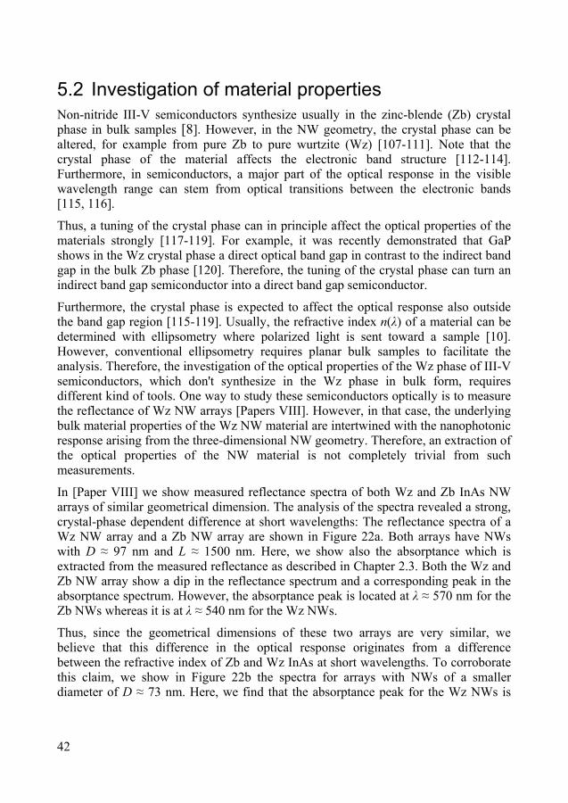
42
5.2 Investigation of material properties Non-nitride III-V semiconductors synthesize usually in the zinc-blende (Zb) crystal phase in bulk samples [8]. However, in the NW geometry, the crystal phase can be altered, for example from pure Zb to pure wurtzite (Wz) [107-111]. Note that the crystal phase of the material affects the electronic band structure [112-114]. Furthermore, in semiconductors, a major part of the optical response in the visible wavelength range can stem from optical transitions between the electronic bands [115, 116].
Thus, a tuning of the crystal phase can in principle affect the optical properties of the materials strongly [117-119]. For example, it was recently demonstrated that GaP shows in the Wz crystal phase a direct optical band gap in contrast to the indirect band gap in the bulk Zb phase [120]. Therefore, the tuning of the crystal phase can turn an indirect band gap semiconductor into a direct band gap semiconductor.
Furthermore, the crystal phase is expected to affect the optical response also outside the band gap region [115-119]. Usually, the refractive index n(λ) of a material can be determined with ellipsometry where polarized light is sent toward a sample [10]. However, conventional ellipsometry requires planar bulk samples to facilitate the analysis. Therefore, the investigation of the optical properties of the Wz phase of III-V semiconductors, which don't synthesize in the Wz phase in bulk form, requires different kind of tools. One way to study these semiconductors optically is to measure the reflectance of Wz NW arrays [Papers VIII]. However, in that case, the underlying bulk material properties of the Wz NW material are intertwined with the nanophotonic response arising from the three-dimensional NW geometry. Therefore, an extraction of the optical properties of the NW material is not completely trivial from such measurements.
In [Paper VIII] we show measured reflectance spectra of both Wz and Zb InAs NW arrays of similar geometrical dimension. The analysis of the spectra revealed a strong, crystal-phase dependent difference at short wavelengths: The reflectance spectra of a Wz NW array and a Zb NW array are shown in Figure 22a. Both arrays have NWs with D ≈ 97 nm and L ≈ 1500 nm. Here, we show also the absorptance which is extracted from the measured reflectance as described in Chapter 2.3. Both the Wz and Zb NW array show a dip in the reflectance spectrum and a corresponding peak in the absorptance spectrum. However, the absorptance peak is located at λ ≈ 570 nm for the Zb NWs whereas it is at λ ≈ 540 nm for the Wz NWs.
Thus, since the geometrical dimensions of these two arrays are very similar, we believe that this difference in the optical response originates from a difference between the refractive index of Zb and Wz InAs at short wavelengths. To corroborate this claim, we show in Figure 22b the spectra for arrays with NWs of a smaller diameter of D ≈ 73 nm. Here, we find that the absorptance peak for the Wz NWs is
43
located at λ ≈ 470 nm. In strong contrast, the absorptance spectrum for the Zb NWs does not show a peak, and we find a flat response in A and R for λ < 500 nm.
The reflectance dip and the corresponding absorptance peak in Figure 22 are an indication of a strongly absorbing nanophotonic resonance. As detailed in Chapter 4.3.5, the resonance wavelength is expected to depend on the refractive index and the diameter of the NWs. Thus, for λ < 500 nm, the difference between the bulk optical properties of Zb and Wz InAs is so large that we can enable or disable nanophotonic resonances by the design for the crystal phase (see figure 22b).
Figure 22. Optical response of Wz and Zb InAs NW arrays of (a) D ≈ 97 nm and L ≈ 1500 nm and (b) D ≈ 73 nm and L ≈ 2000 nm; see Figure 16a for a schematic and [Paper VIII] for details of the growth of the NWs. Here, we show the measured reflectance spectrum and the absorptance spectrum that is extracted from the measured reflectance spectrum as described in Chapter 2.3 and [Paper VII].
From the blue-shift of the absorptance peak with decreasing D in Wz NW arrays, we could actually extract an estimate for the real part of the refractive index of Wz InAs [Paper VIII]. Furthermore, from the measured reflectance values at the reflectance dip, we extracted an estimate for the imaginary part of the refractive index. These estimates for the refractive index indicated considerable differences in the electronic band structure between Wz and Zb InAs: In the ZB phase, the band structure of InAs shows a critical point (with nearly parallel conduction and valence band) for the absorption of photons with λ ≈ 450 nm. Our results indicated that this critical point is shifted to considerably higher energies for Wz InAs [Paper VIII]. Thus, reflectance measurements of NW arrays could yield insight into the electronic band structure and refractive index of materials that are hard to study otherwise. Such knowledge is of importance when designing opto-electronic devices based on those materials.
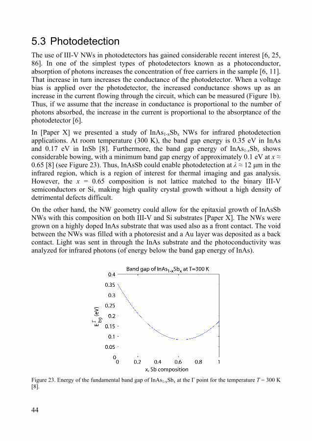
44
5.3 Photodetection The use of III-V NWs in photodetectors has gained considerable recent interest [6, 25, 86]. In one of the simplest types of photodetectors known as a photoconductor, absorption of photons increases the concentration of free carriers in the sample [6, 11]. That increase in turn increases the conductance of the photodetector. When a voltage bias is applied over the photodetector, the increased conductance shows up as an increase in the current flowing through the circuit, which can be measured (Figure 1b). Thus, if we assume that the increase in conductance is proportional to the number of photons absorbed, the increase in the current is proportional to the absorptance of the photodetector [6].
In [Paper X] we presented a study of InAs1-xSbx NWs for infrared photodetection applications. At room temperature (300 K), the band gap energy is 0.35 eV in InAs and 0.17 eV in InSb [8]. Furthermore, the band gap energy of InAs1-xSbx shows considerable bowing, with a minimum band gap energy of approximately 0.1 eV at x ≈ 0.65 [8] (see Figure 23). Thus, InAsSb could enable photodetection at λ ≈ 12 μm in the infrared region, which is a region of interest for thermal imaging and gas analysis. However, the x = 0.65 composition is not lattice matched to the binary III-V semiconductors or Si, making high quality crystal growth without a high density of detrimental defects difficult.
On the other hand, the NW geometry could allow for the epitaxial growth of InAsSb NWs with this composition on both III-V and Si substrates [Paper X]. The NWs were grown on a highly doped InAs substrate that was used also as a front contact. The void between the NWs was filled with a photoresist and a Au layer was deposited as a back contact. Light was sent in through the InAs substrate and the photoconductivity was analyzed for infrared photons (of energy below the band gap energy of InAs).
Figure 23. Energy of the fundamental band gap of InAs1-xSbx at the Γ point for the temperature T = 300 K [8].
45
From the measurements [Paper X], it was seen that the spectrally resolved photoconductivity showed a peak whose position depended on the NW diameter. These findings were in good agreement with the modeled absorptance of the NWs, which showed a corresponding absorptance peak due to the resonant excitation of the HE11 waveguide mode in the NWs. In the experiments, diameters on the order of 700 nm were used, which positioned the peak at approximately λ ≈ 4500 nm. The prediction was that diameters up to D ≈ 1600 nm would be needed to shift the absorptance peak to the room temperature band gap of InAs0.35Sb0.65.
Notice that if D << λ would have applied for the NWs, which holds for typical NW diameters of D ≈ 100 nm when λ ≈ 10 μm, the absorption per volume material in the NWs could have been up to 200 times lower than when the HE11 resonance condition is reached by tuning D (Chapter 4.3.5 and [Paper IV]). Such a difference translates into requiring 200 times longer NWs at the same NW area coverage f to compensate for the reduced absorption, shifting the required NW length from the range of a few micrometers to the millimeter range. This highlights how important it is to carefully take into account the nanophotonic effects when designing photodetectors based on NW arrays.
5.4 Solar cells As discussed in Chapter 1, the NW geometry could facilitate the epitaxial growth of material combinations that are not possible to combine in thin films. NW arrays have been investigated experimentally for some time for solar cell applications [32, 121-124]. The ultimate prospect with NW solar cells is to grow, on top a substrate of a cheap and abundant material, a multi-junction solar cell that is band gap matched efficiently to the solar spectrum [32]. However, for a long time, the efficiency of fabricated single-junction NW cells, which are expected to be simpler to optimize than multi-junction cells, was quite limited and showed values in the range of 4 % [122-124].
In the nanophotonic regime where λ ≈ D, light that would travel between the NWs in a ray-optics description can interact efficiently with the NWs if λ ≈ p. Such interaction is shown for example in Figure 16 where the modeled absorptance of the InP NWs shows values very close to 100 % even though the NW area coverage is only 22 %. Furthermore, it has been shown experimentally that the light trapping in NW arrays could enhance considerably the optical path length in the NW array, with an estimated upper bound of a factor of 73 [125].
Thus, NWs appear promising for the absorption of light in solar cells. As discussed in Chapter 4.3.5, a diameter of D ≈ 180 nm optimizes the absorption of sun light in InP NW array solar cells [Paper V]. Indeed, such a diameter gave a (for NW solar cells) very high efficiency of 13.8 % under 1 sun (1000 W/m2) illumination [Paper XI]. The solar cell consisted of an array of InP NWs with an p-i-n junction in each NW in the

46
axial direction. The NWs were grown on an InP substrate at a NW area coverage of f = 12 % (see Figures 3d and 3e for SEM images taken, respectively, before and after the processing with a SiO2 insulating layer and an ITO top-contact layer). To enhance the extracted current from the cell, we showed both experimentally and theoretically that it is of outmost importance to reduce the length of the highly doped n type top region [Paper XI]. Presumably, the high dopant concentration in that region leads to strong recombination of photogenerated charge carriers before they can contribute to the current.
Figure 24. (a) IV curves of the InP NW array solar cell of 13.8 % in efficiency [Paper XI] and the GaAs NW array solar cell of 6.6 % in efficiency [126]. (b) EQE spectra of the solar cells in (a). Note that the values shown for the GaAs cell were extracted from the electronic version of the corresponding paper [126] using the software Engauge Digitizer (http://digitizer.sourceforge.net).
The InP NW array solar cell showed a short circuit current density of 24.6 mA/cm2 under 1 sun illumination (see Figure 24a). That value is 71 % of the theoretical maximum of 34.5 mA/cm2 for InP assuming that each incident photon can contribute a maximum of one electron-hole pair to the current [Paper XI]. Thus, despite covering only 12 % of the surface, these NWs convert incident photons efficiently into current.
Later, a comparable current density of 24.3 mA/cm2 was demonstrated for a GaAs NW-array solar cell [126] (see Figure 24a). This current density is actually more impressive than that with the InP NWs since the theoretical maximum is lower for GaAs (31 mA/cm2) due to its slightly higher band gap energy. Furthermore, both material systems showed very similar external quantum efficiency (EQE) spectra with high EQE values of approximately 80 % for a large part of the above band gap region (see Figure 24b). However, the GaAs NWs [126] showed a considerably lower open circuit voltage (0.44 V) and fill factor (0.62) compared to the InP NWs (0.78 V and 0.72, respectively) (see Figure 24a). This gives for the GaAs NWs a considerably lower efficiency of 6.6 % [126].
47
This highlights how important it is to consider the IV-characteristics of the solar cell. For high efficiency, it is not enough to have efficient absorption of light, leading to a high short circuit current density and a high EQE: At the maximum power point of the solar cell, the output power is given by the product of the short circuit current, the open circuit voltage, and the fill factor.
5.4.1 Emission of light in solar cells
We note here that the research presented in this thesis has concentrated heavily on the coupling of light into NW arrays and the subsequent absorption. However, also the emission of light is of importance for a solar cell: In the absence of parasitic non-radiative recombination, the ultimate limit on efficiency is set by the balance between charge carriers created by the incident light, the current extracted from the cell, and the emission of photons from the cell. In this picture the solar cell is thus considered as a black-box and we do not care about its internal working mechanism [3, 14, 127-129]. Importantly, the emission of photons is enhanced exponentially with increasing voltage over the solar cell [3]. Therefore, when calculating the ultimate limit for efficiency, it is the emission of photons that limits the open circuit voltage and the fill factor; and therefore also the efficiency of the solar cell. Thus, by limiting the emission of photons, the efficiency could increase.
However, from the Kirchoffs's laws, the emissivity equals the absorptance for both polarizations and all propagation directions of light [14, 127]. Therefore, the emission of photons cannot be completely prohibited since that would prohibit the absorption of incident light. On the other hand, by reducing the emissivity for solid angles outside of the cone from which light is incident, it is possible to suppress the number of emitted photons without reducing the number of absorbed photons [55, 127]. Thus, an interesting future avenue for research would be to investigate how the emission properties of NW arrays could be tuned to enhance their ultimate efficiency limit.

49
6 Conclusions We have investigated both experimentally and theoretically the coupling of light into absorbing III-V NW arrays and identified a very strong dependence of the NW diameter on the absorption of light. Starting from small diameter NWs and moving toward large diameter NWs, the optical response shifts from that described by electrostatics to that described by geometrical optics. Between these two limit cases lies the nanophotonic regime where optical resonances can show up.
In the electrostatic limit, the large refractive index of the NWs causes screening of the incident electric field from the interior of the NWs, leading to more than 10 times weaker absorption per volume semiconductor material than in a bulk sample. In contrast, at nanophotonic resonances, the absorption can be more than 20 times stronger than in a bulk sample. Thus, the difference in the absorption per volume semiconductor material can be more than a factor of 200 depending on the choice of the NW diameter.
By placing such well-absorbing, diameter-dependent nanophotonic resonances close to the band gap wavelength of the NWs, the absorption of sun light can be optimized. Such a strategy for the design of the NW geometry facilitated the fabrication of InP NW solar cells with a, for NW arrays, very high efficiency of 13.8 %. Similarly, by tuning the diameter of InAsSb NWs, resonant absorption in the near-infrared region could be demonstrated. Such absorption lead to a peak in the spectrally resolved photoconductivity. However, due to the spectral region considered, the diameter of the InAsSb NWs was increased to 700 nm, with a proposed optimized diameter of 1600 nm.
We demonstrated also how ex-situ reflection measurements can be used for determining both the length and diameter of NWs in arrays, and their variations over large-area samples. Such a metrology tool should be able to enhance the nanostructure fabrication process, especially if applied in-situ during NW growth.
Finally, we studied the reflection of light from Zb and Wz InAs NW arrays and extracted the absorptance of the NWs from these measurements. This novel measurement and analysis technique allowed us to study the optical properties of Wz InAs, which is not easily done in bulk samples since bulk InAs, as most non-nitride III-V semiconductors, synthesizes in the Zb phase. Our study revealed that the optical properties of InAs are strongly dependent on the crystal phase in the short wavelength region. The difference between Wz and Zb NWs can be so large that nanophotonic resonances can be enabled or disabled by a suitable choice for the crystal phase. We believe that this analysis technique holds promise for mapping out details about the optical transitions and the electronic band structure of the different crystal phases of semiconductor materials.


51
References [1] M. A. Green, K. Emery, Y. Hishikawa, W. Warta, and E. D. Dunlop, Solar cell efficiency
tables (version 41). Progress in Photovoltaics: Research and Applications 21, 1 (2013).
[2] Air Mass 1.5 Spectra; (American Society for Testing and Materials, http://rredc.nrel.gov/solar/spectra/am1.5/, 2013).
[3] W. Shockley and H. J. Queisser, Detailed balance limit of efficiency of p-n junction solar cells. Journal of Applied Physics 32, 510 (1961).
[4] C. Kittel, Introduction to solid state physics; (Wiley, 2005).
[5] S. M. Sze and K. K. Ng, Physics of semiconductor devices; (Wiley, 2006).
[6] C. Soci, A. Zhang, X.-Y. Bao, H. Kim, Y. Lo, and D. Wang, Nanowire photodetectors. Journal of Nanoscience and Nanotechnology 10, 1430 (2010).
[7] L. Samuelson, Self-forming nanoscale devices. Materials Today 6, 22 (2003).
[8] I. Vurgaftman, J. R. Meyer, and L. R. Ram-Mohan, Band parameters for III–V compound semiconductors and their alloys. Journal of Applied Physics 89, 5815 (2001).
[9] O. J. Glembocki and H. Piller, "Indium phosphide (InP)" in Handbook of optical constants of solids, Palik, E. D., ed. (Academic, 1985).
[10] D. F. Edwards, "Silicon (Si)" in Handbook of optical constants of solids, Palik, E. D., ed. (Academic, 1985).
[11] B. E. A. Saleh and M. C. Teich, Fundamentals of photonics; (Wiley, 2007).
[12] D. J. Dunstan, Strain and strain relaxation in semiconductors. Journal of Materials Science: Materials in Electronics 8, 337 (1997).
[13] G. H. Olsen, Interfacial lattice mismatch effects in III–V compounds. Journal of Crystal Growth 31, 223 (1975).
[14] S. Sandhu, Z. Yu, and S. Fan, Detailed balance analysis of nanophotonic solar cells. Optics Express 21, 1209 (2013).
[15] W. Seifert, N. Carlsson, M. Miller, M.-E. Pistol, L. Samuelson, and L. R. Wallenberg, In-situ growth of quantum dot structures by the Stranski-Krastanow growth mode. Progress in Crystal Growth and Characterization of Materials 33, 423 (1996).
[16] K. Pinardi, U. Jain, S. C. Jain, H. E. Maes, R. Van Overstraeten, and M. Willander, Critical thickness and strain relaxation in lattice mismatched II-VI semiconductor layers. Journal of Applied Physics 83, 4724 (1998).
[17] G. Kästner and U. Gösele, Stress and dislocations at cross-sectional heterojunctions in a cylindrical nanowire. Philosophical Magazine 84, 3803 (2004).
[18] M. T. Bjork, B. J. Ohlsson, T. Sass, A. I. Persson, C. Thelander, M. H. Magnusson, K. Deppert, L. R. Wallenberg, and L. Samuelson, One-dimensional heterostructures in semiconductor nanowhiskers. Applied Physics Letters 80, 1058 (2002).
[19] P. Caroff, M. E. Messing, M. B. Borg, K. A. Dick, K. Deppert, and L.-E. Wernersson, InSb heterostructure nanowires: MOVPE growth under extreme lattice mismatch. Nanotechnology 20, 495606 (2009).

52
[20] K. A. Dick, S. Kodambaka, M. C. Reuter, K. Deppert, L. Samuelson, W. Seifert, L. R. Wallenberg, and F. M. Ross, The morphology of axial and branched nanowire heterostructures. Nano Letters 7, 1817 (2007).
[21] M. Heurlin, P. Wickert, S. Fält, M. T. Borgström, K. Deppert, L. Samuelson, and M. H. Magnusson, Axial InP nanowire tandem junction grown on a silicon substrate. Nano Letters 11, 2028 (2011).
[22] C. P. T. Svensson, T. Mårtensson, J. Trägårdh, C. Larsson, M. Rask, D. Hessman, L. Samuelson, and J. Ohlsson, Monolithic GaAs/InGaP nanowire light emitting diodes on silicon. Nanotechnology 19, 305201 (2008).
[23] K. Tomioka, J. Motohisa, S. Hara, K. Hiruma, and T. Fukui, GaAs/AlGaAs core multishell nanowire-based light-emitting diodes on Si. Nano Letters 10, 1639 (2010).
[24] T. Mårtensson, C. P. T. Svensson, B. A. Wacaser, M. W. Larsson, W. Seifert, K. Deppert, A. Gustafsson, L. R. Wallenberg, and L. Samuelson, Epitaxial III−V nanowires on silicon. Nano Letters 4, 1987 (2004).
[25] L. Vj, J. Oh, A. P. Nayak, A. M. Katzenmeyer, K. H. Gilchrist, S. Grego, N. P. Kobayashi, S. Y. Wang, A. A. Talin, N. K. Dhar, and M. S. Islam, A perspective on nanowire photodetectors: current status, future challenges, and opportunities. IEEE Journal of Selected Topics in Quantum Electronics 17, 1002 (2011).
[26] R. S. Wagner and W. C. Ellis, Vapor-liquid-solid mechanism of single crystal growth. Applied Physics Letters 4, 89 (1964).
[27] H. J. Fan, P. Werner, and M. Zacharias, Semiconductor nanowires: from self-organization to patterned growth. Small 2, 700 (2006).
[28] K. A. Dick, A review of nanowire growth promoted by alloys and non-alloying elements with emphasis on Au-assisted III–V nanowires. Progress in Crystal Growth and Characterization of Materials 54, 138 (2008).
[29] A. Pierret, M. Hocevar, S. L. Diedenhofen, R. E. Algra, E. Vlieg, E. Timmering, C. , M. Verschuuren, A. , G. Immink, W. G., M. Verheijen, A., and E. P. A. M. Bakkers, Generic nano-imprint process for fabrication of nanowire arrays. Nanotechnology 21, 065305 (2010).
[30] T. Mårtensson, P. Carlberg, M. Borgström, L. Montelius, W. Seifert, and L. Samuelson, Nanowire arrays defined by nanoimprint lithography. Nano Letters 4, 699 (2004).
[31] M. Messing, K. Hillerich, J. Bolinsson, K. Storm, J. Johansson, K. Dick, and K. Deppert, A comparative study of the effect of gold seed particle preparation method on nanowire growth. Nano Research 3, 506 (2010).
[32] M. T. Borgström, J. Wallentin, M. Heurlin, S. Fält, P. Wickert, J. Leene, M. H. Magnusson, K. Deppert, and L. Samuelson, Nanowires with promise for photovoltaics. IEEE Journal of Selected Topics in Quantum Electronics 17, 1050 (2011).
[33] J. Wallentin and M. T. Borgström, Doping of semiconductor nanowires. Journal of Materials Research 26, 2142 (2011).
[34] S. Naureen, R. Sanatinia, N. Shahid, and S. Anand, High optical quality InP-based nanopillars fabricated by a top-down approach. Nano Letters 11, 4805 (2011).
[35] J. Zhu, Z. Yu, G. F. Burkhard, C.-M. Hsu, S. T. Connor, Y. Xu, Q. Wang, M. McGehee, S. Fan, and Y. Cui, Optical absorption enhancement in amorphous silicon nanowire and nanocone arrays. Nano Letters 9, 279 (2008).
53
[36] K. Seo, M. Wober, P. Steinvurzel, E. Schonbrun, Y. Dan, T. Ellenbogen, and K. B. Crozier, Multicolored vertical silicon nanowires. Nano Letters 11, 1851 (2011).
[37] E. Yablonovitch, Inhibited spontaneous emission in solid-state physics and electronics. Physical Review Letters 58, 2059 (1987).
[38] J. D. Joannopoulos, S. G. Johnson, J. N. Winn, and R. D. Meade, Photonic crystals: molding the flow of light; (Princeton University Press, 2011).
[39] S. John, Strong localization of photons in certain disordered dielectric superlattices. Physical Review Letters 58, 2486 (1987).
[40] A. Hessel and A. A. Oliner, A new theory of Wood's anomalies on optical gratings. Applied Optics 4, 1275 (1965).
[41] S. L. Diedenhofen, O. T. A. Janssen, G. Grzela, E. P. A. M. Bakkers, and J. Gómez Rivas, Strong geometrical dependence of the absorption of light in arrays of semiconductor nanowires. ACS Nano 5, 2316 (2011).
[42] Y. Fontana, G. Grzela, E. P. A. M. Bakkers, and J. Gómez Rivas, Mapping the directional emission of quasi-two-dimensional photonic crystals of semiconductor nanowires using Fourier microscopy. Physical Review B 86, 245303 (2012).
[43] A. Iqbal, J. P. Beech, N. Anttu, M.-E. Pistol, L. Samuelson, M. T. Borgström, and A. Yartsev, Photoluminescence study of as-grown vertically standing wurtzite InP nanowire ensembles. Nanotechnology 24, 115706 (2013).
[44] R. Sanatinia, K. M. Awan, S. Naureen, N. Anttu, E. Ebraert, and S. Anand, GaAs nanopillar arrays with suppressed broadband reflectance and high optical quality for photovoltaic applications. Optical Materials Express 2, 1671 (2012).
[45] A. R. Madaria, M. Yao, C. Chi, N. Huang, C. Lin, R. Li, M. L. Povinelli, P. D. Dapkus, and C. Zhou, Toward optimized light utilization in nanowire arrays using scalable nanosphere lithography and selected area growth. Nano Letters 12, 2839 (2012).
[46] Z. Fan, R. Kapadia, P. W. Leu, X. Zhang, Y.-L. Chueh, K. Takei, K. Yu, A. Jamshidi, A. A. Rathore, D. J. Ruebusch, M. Wu, and A. Javey, Ordered arrays of dual-diameter nanopillars for maximized optical absorption. Nano Letters 10, 3823 (2010).
[47] K. E. Plass, M. A. Filler, J. M. Spurgeon, B. M. Kayes, S. Maldonado, B. S. Brunschwig, H. A. Atwater, and N. S. Lewis, Flexible polymer-embedded Si wire arrays. Advanced Materials 21, 325 (2009).
[48] A. C. Scofield, J. N. Shapiro, A. Lin, A. D. Williams, P.-S. Wong, B. L. Liang, and D. L. Huffaker, Bottom-up photonic crystal cavities formed by patterned III–V nanopillars. Nano Letters 11, 2242 (2011).
[49] M. Khorasaninejad, N. Abedzadeh, J. Walia, S. Patchett, and S. S. Saini, Color matrix refractive index sensors using coupled vertical silicon nanowire arrays. Nano Letters 12, 4228 (2012).
[50] S. L. Diedenhofen, R. E. Algra, E. P. A. M. Bakkers, and J. G. Rivas, Strong modification of the reflection from birefringent layers of semiconductor nanowires by nanoshells. Applied Physics Letters 99, 201108 (2011).
[51] E. D. Palik and R. T. Holm, "Indium arsenide (InAs)" in Handbook of optical constants of solids, Palik, E. D., ed. (Academic, 1985), pp. 479-489.
54
[52] M. T. Borgström, V. Zwiller, E. Müller, and A. Imamoglu, Optically bright quantum dots in single nanowires. Nano Letters 5, 1439 (2005).
[53] M. D. Kelzenberg, S. W. Boettcher, J. A. Petykiewicz, D. B. Turner-Evans, M. C. Putnam, E. L. Warren, J. M. Spurgeon, R. M. Briggs, N. S. Lewis, and H. A. Atwater, Enhanced absorption and carrier collection in Si wire arrays for photovoltaic applications. Nature Communications 9, 239 (2010).
[54] E. D. Kosten, E. L. Warren, and H. A. Atwater, Ray optical light trapping in silicon microwires: exceeding the 2n2 intensity limit. Optics Express 19, 3316 (2011).
[55] J. Kupec and B. Witzigmann, Computational electromagnetics for nanowire solar cells. Journal of Computational Electronics 11, 153 (2012).
[56] G. Brönstrup, C. Leiterer, N. Jahr, C. Gutsche, A. Lysov, I. Regolin, W. Prost, F. J. Tegude, W. Fritzsche, and S. Christiansen, A precise optical determination of nanoscale diameters of semiconductor nanowires. Nanotechnology 22, 385201 (2011).
[57] L. Junshuai, Y. HongYu, and L. Yali, Solar energy harnessing in hexagonally arranged Si nanowire arrays and effects of array symmetry on optical characteristics. Nanotechnology 23, 194010 (2012).
[58] J. Li, H. Yu, S. M. Wong, X. Li, G. Zhang, P. G.-Q. Lo, and D.-L. Kwong, Design guidelines of periodic Si nanowire arrays for solar cell application. Applied Physics Letters 95, 243113 (2009).
[59] J. Kupec, R. L. Stoop, and B. Witzigmann, Light absorption and emission in nanowire array solar cells. Optics Express 18, 27589 (2010).
[60] J. Kupec and B. Witzigmann, Dispersion, wave propagation and efficiency analysis of nanowire solar cells. Optics Express 17, 10399 (2009).
[61] K. Yee, Numerical solution of initial boundary value problems involving Maxwell's equations in isotropic media. IEEE Transactions on Antennas and Propagation 14, 302 (1966).
[62] H. Bao and X. Ruan, Optical absorption enhancement in disordered vertical silicon nanowire arrays for photovoltaic applications. Optics Letters 35, 3378 (2010).
[63] Q. G. Du, C. H. Kam, H. V. Demir, H. Y. Yu, and X. W. Sun, Broadband absorption enhancement in randomly positioned silicon nanowire arrays for solar cell applications. Optics Letters 36, 1884 (2011).
[64] L. Wen, Z. Zhao, X. Li, Y. Shen, H. Guo, and Y. Wang, Theoretical analysis and modeling of light trapping in high efficicency GaAs nanowire array solar cells. Applied Physics Letters 99, 143116 (2011).
[65] M. Khorasaninejad, N. Abedzadeh, J. Sun, J. N. Hilfiker, and S. S. Saini, Polarization resolved reflection from ordered vertical silicon nanowire arrays. Optics Letters 37, 2961 (2012).
[66] A. Hadiseh, C. A. Ashwin, and A. D. Jennifer, Optimized light absorption in Si wire array solar cells. Journal of Optics 14, 024006 (2012).
[67] P. Kailuweit, M. Peters, J. Leene, K. Mergenthaler, F. Dimroth, and A. W. Bett, Numerical simulations of absorption properties of InP nanowires for solar cell applications. Progress in Photovoltaics: Research and Applications 20, 945 (2012).

55
[68] C. Lin and M. L. Povinelli, Optical absorption enhancement in silicon nanowire arrays with a large lattice constant for photovoltaic applications. Optics Express 17, 19371 (2009).
[69] N. Huang, C. Lin, and M. L. Povinelli, Broadband absorption of semiconductor nanowire arrays for photovoltaic applications. Journal of Optics 14, 024004 (2012).
[70] E. Noponen and J. Turunen, Eigenmode method for electromagnetic synthesis of diffractive elements with three-dimensional profiles. Journal of the Optical Society of America A 11, 2494 (1994).
[71] K. Knop, Rigorous diffraction theory for transmission phase gratings with deep rectangular grooves. Journal of the Optical Society of America 68, 1206 (1978).
[72] L. Li, New formulation of the Fourier modal method for crossed surface-relief gratings. Journal of the Optical Society of America A 14, 2758 (1997).
[73] L. Li, Multilayer modal method for diffraction gratings of arbitrary profile, depth, and permittivity. Journal of the Optical Society of America A 10, 2581 (1993).
[74] A. A. Barybin, Modal expansions and orthogonal complements in the theory of complex media waveguide excitation by external sources for isotropic, anisotropic, and bianisotropic media. Progress in Electromagnetics Research 19, 241 (1998).
[75] L. Li, Use of Fourier series in the analysis of discontinuous periodic structures. Journal of the Optical Society of America A 13, 1870 (1996).
[76] E. Popov and M. Nevière, Maxwell equations in Fourier space: fast-converging formulation for diffraction by arbitrary shaped, periodic, anisotropic media. Journal of the Optical Society of America A 18, 2886 (2001).
[77] R. Magnusson and T. K. Gaylord, Equivalence of multiwave coupled-wave theory and modal theory for periodic-media diffraction. Journal of the Optical Society of America 68, 1777 (1978).
[78] B. Bai and L. Li, Group-theoretic approach to enhancing the Fourier modal method for crossed gratings with square symmetry. Journal of the Optical Society of America A 23, 572 (2006).
[79] D. Y. K. Ko and J. C. Inkson, Matrix method for tunneling in heterostructures: resonant tunneling in multilayer systems. Physical Review B 38, 9945 (1988).
[80] D. M. Whittaker and I. S. Culshaw, Scattering-matrix treatment of patterned multilayer photonic structures. Physical Review B 60, 2610 (1999).
[81] M. Liscidini, D. Gerace, L. C. Andreani, and J. E. Sipe, Scattering-matrix analysis of periodically patterned multilayers with asymmetric unit cells and birefringent media. Physical Review B 77, 035324 (2008).
[82] S. G. Tikhodeev, A. L. Yablonskii, E. A. Muljarov, N. A. Gippius, and T. Ishihara, Quasiguided modes and optical properties of photonic crystal slabs. Physical Review B 66, 045102 (2002).
[83] B. Bai and L. Li, Reduction of computation time for crossed-grating problems: a group-theoretic approach. Journal of the Optical Society of America A 21, 1886 (2004).
[84] V. Myroshnychenko, J. Rodriguez-Fernandez, I. Pastoriza-Santos, A. M. Funston, C. Novo, P. Mulvaney, L. M. Liz-Marzan, and F. J. Garcia de Abajo, Modelling the optical response of gold nanoparticles. Chemical Society Reviews 37, 1792 (2008).

56
[85] B. Wang and P. W. Leu, Tunable and selective resonant absorption in vertical nanowires. Optics Letters 37, 3756 (2012).
[86] J. Wang, M. S. Gudiksen, X. Duan, Y. Cui, and C. M. Lieber, Highly polarized photoluminescence and photodetection from single indium phosphide nanowires. Science 293, 1455 (2001).
[87] P. M. Wu, L. Samuelson, and H. Linke, Toward 3D integration of 1D conductors: junctions of InAs nanowires. Journal of Nanomaterials 2011, 268149 (2011).
[88] F. J. García-Vidal, J. M. Pitarke, and J. B. Pendry, Effective medium theory of the optical properties of aligned carbon nanotubes. Physical Review Letters 78, 4289 (1997).
[89] Y. Yu, V. E. Ferry, A. P. Alivisatos, and L. Cao, Dielectric core–shell optical antennas for strong solar absorption enhancement. Nano Letters 12, 3674 (2012).
[90] The Landolt Börnstein database; (Springer Materials).
[91] L. Hu and G. Chen, Analysis of optical absorption in silicon nanowire arrays for photovoltaic applications. Nano Letters 7, 3249 (2007).
[92] P. B. Clapham and M. C. Hutley, Reduction of lens reflexion by the “moth eye” principle. Nature 244, 281 (1973).
[93] J. Zhu, Z. Yu, S. Fan, and Y. Cui, Nanostructured photon management for high performance solar cells. Materials Science and Engineering: R: Reports 70, 330 (2010).
[94] S. L. Diedenhofen, G. Vecchi, R. E. Algra, A. Hartsuiker, O. L. Muskens, G. Immink, E. P. A. M. Bakkers, W. L. Vos, and J. G. Rivas, Broad-band and omnidirectional antireflection coatings based on semiconductor nanorods. Advanced Materials 21, 973 (2009).
[95] S. Chattopadhyay, Y. F. Huang, Y. J. Jen, A. Ganguly, K. H. Chen, and L. C. Chen, Anti-reflecting and photonic nanostructures. Materials Science and Engineering: R: Reports 69, 1 (2010).
[96] E. Yablonovitch, Statistical ray optics. Journal of the Optical Society of America 72, 899 (1982).
[97] Z. Yu, A. Raman, and S. Fan, Fundamental limit of nanophotonic light trapping in solar cells. Proceedings of the National Academy of Sciences 107, 17491 (2010).
[98] S. Mokkapati and K. R. Catchpole, Nanophotonic light trapping in solar cells. Journal of Applied Physics 112, 101101 (2012).
[99] Z. Yu, A. Raman, and S. Fan, Fundamental limit of light trapping in grating structures. Optics Express 18, A366 (2010).
[100] G. Cao and Y. Wang, Nanostructures and nanomaterials - synthesis, properties and applications; (World Scientific, 2011).
[101] M. Auffan, J. Rose, J.-Y. Bottero, G. V. Lowry, J.-P. Jolivet, and M. R. Wiesner, Towards a definition of inorganic nanoparticles from an environmental, health and safety perspective. Nature Nanotechnology 4, 634 (2009).
[102] S. M. Stevens, P. Cubillas, K. Jansson, O. Terasaki, and M. W. Anderson, Nanoscale electron beam damage studied by atomic force microscopy. Journal of Physical Chemistry C 113, 18441 (2009).
[103] E. Abbe, Beiträge zur Theorie des Mikroskops und der mikroskopischen Wahrnehmung. Archiv für Mikroskopische Anatomie 9, 413 (1873).

57
[104] D. B. Kushev, N. N. Zheleva, Y. Demakopoulou, and D. Siapkas, A new method for the determination of the thickness, the optical constants and the relaxation time of weakly absorbing semiconducting thin films. Infrared Physics 26, 385 (1986).
[105] J. C. Manifacier, J. Gasiot, and J. P. Fillard, A simple method for the determination of the optical constants n, k and the thickness of a weakly absorbing thin film. Journal of Physics E: Scientific Instruments 9, 1002 (1976).
[106] C. F. Bohren, E. E. Clothiaux, and D. R. Huffman, Absorption and scattering of light by small particles; (Wiley VCH Verlag GmbH, 2010).
[107] P. Caroff, K. A. Dick, J. Johansson, M. E. Messing, K. Deppert, and L. Samuelson, Controlled polytypic and twin-plane superlattices in III−V nanowires. Nature Nanotechnology 4, 50 (2009).
[108] P. Caroff, J. Bolinsson, and J. Johansson, Crystal phases in III−V nanowires: from random toward engineered polytypism. IEEE Journal of Selected Topics in Quantum Electronics 17, 829 (2011).
[109] R. E. Algra, M. A. Verheijen, M. T. Borgstrom, L.-F. Feiner, G. Immink, W. J. P. van Enckevort, E. Vlieg, and E. P. A. M. Bakkers, Twinning superlattices in indium phosphide nanowires. Nature 456, 369 (2008).
[110] K. A. Dick, J. Bolinsson, M. E. Messing, S. Lehmann, J. Johansson, and P. Caroff, Parameter space mapping of InAs nanowire crystal structure. Journal of Vacuum Science and Technology B 29, 04D103 (2011).
[111] F. Glas, J.-C. Harmand, and G. Patriarche, Why does wurtzite form in nanowires of III–V zinc blende semiconductors? Physical Review Letters 99, 146101 (2007).
[112] A. De and C. E. Pryor, Predicted band structures of III−V semiconductors in the wurtzite phase. Physical Review B 81, 155210 (2010).
[113] A. Belabbes, C. Panse, J. Furthmüller, and F. Bechstedt, Electronic bands of III–V semiconductor polytypes and their alignment. Physical Review B 86, 075208 (2012).
[114] S. Q. Wang and H. Q. Ye, A plane-wave pseudopotential study on III–V zinc-blende and wurtzite semiconductors under pressure. Journal of Physics: Condensed Matter 14, 9579 (2002).
[115] A. De and C. E. Pryor, Optical dielectric functions of wurtzite III−V semiconductors. Physical Review B 85, 125201 (2012).
[116] M. Cardona, Linear optical response of semiconductors. Journal of Electronic Materials 22, 27 (1993).
[117] M. Roppischer, R. Goldhahn, G. Rossbach, P. Schley, C. Cobet, N. Esser, T. Schupp, K. Lischka, and D. J. As, Dielectric function of zinc-blende AlN from 1 to 20 eV: band gap and van Hove singularities. Journal of Applied Physics 106, 076104 (2009).
[118] M. E. Lin, B. N. Sverdlov, S. Strite, H. Morkov, and A. E. Drakin, Refractive indices of wurtzite and zincblende GaN. Electronics Letters 29, 1759 (1993).
[119] C. Cobet, R. Goldhahn, W. Richter, and N. Esser, Identification of van Hove singularities in the GaN dielectric function: a comparison of the cubic and hexagonal phase. Physica Status Solidi B 246, 1440 (2009).

58
[120] S. Assali, I. Zardo, S. Plissard, D. Kriegner, M. A. Verheijen, G. Bauer, A. Meijerink, A. Belabbes, F. Bechstedt, J. E. M. Haverkort, and E. P. A. M. Bakkers, Direct band gap wurtzite gallium phosphide nanowires. Nano Letters 12, 1559 (2013).
[121] L. Tsakalakos, J. Balch, J. Fronheiser, M.-Y. Shih, S. F. LeBoeuf, M. Pietrzykowski, P. J. Codella, B. A. Korevaar, O. V. Sulima, J. Rand, A. Davuluru, and U. Rapol, Strong broadband optical absorption in silicon nanowire films. Journal of Nanophotonics 1, 013552 (2007).
[122] G. Mariani, P.-S. Wong, A. M. Katzenmeyer, F. Léonard, J. Shapiro, and D. L. Huffaker, Patterned radial GaAs nanopillar solar cells. Nano Letters 11, 2490 (2011).
[123] H. Goto, K. Nosaki, K. Tomioka, S. Hara, K. Hiruma, J. Motohisa, and T. Fukui, Growth of core-shell InP nanowires for photovoltaic application by selective-area metal organic vapor phase epitaxy. Applied Physics Express 2, 035004
[124] J. A. Czaban, D. A. Thompson, and R. R. LaPierre, GaAs core−shell nanowires for photovoltaic applications. Nano Letters 9, 148 (2008).
[125] E. Garnett and P. Yang, Light trapping in silicon nanowire solar cells. Nano Letters 10, 1082 (2010).
[126] G. Mariani, A. C. Scofield, C.-H. Hung, and D. L. Huffaker, GaAs nanopillar-array solar cells employing in situ surface passivation. Nature Communications 4, 1497 (2013).
[127] E. D. Kosten, J. H. Atwater, J. Parsons, A. Polman, and H. A. Atwater, Highly efficient GaAs solar cells by limiting light emission angle. Light: Science and Applications 2, e45 (2013).
[128] O. D. Miller, E. Yablonovitch, and S. R. Kurtz, Strong internal and external luminescence as solar cells approach the Shockley-Queisser limit. IEEE Journal of Photovoltaics 2, 303 (2012).
[129] E. Yablonovitch, O. D. Miller, and S. R. Kurtz, A great solar cell also needs to be a great LED: external fluorescence leads to new efficiency record. AIP Conference Proceedings 1519, 9 (2013).