Embed Size (px)
Citation preview

NANO FABRICATION LABORATORY SEOUL NATIONAL UNIVERSITY
Nanofabrication process using electron beam lithography
(AIPEL; Atomic Image Projection E-beam Lithography)
School of Materials Science and EngineeringSeoul National University
Ki-Bum Kim

Nano Fabrication Laboratory SEOUL NATIONAL UNIVERSITY
(A report by the interagency working group on nanoscience, engineering and technology, Feb., 2000)
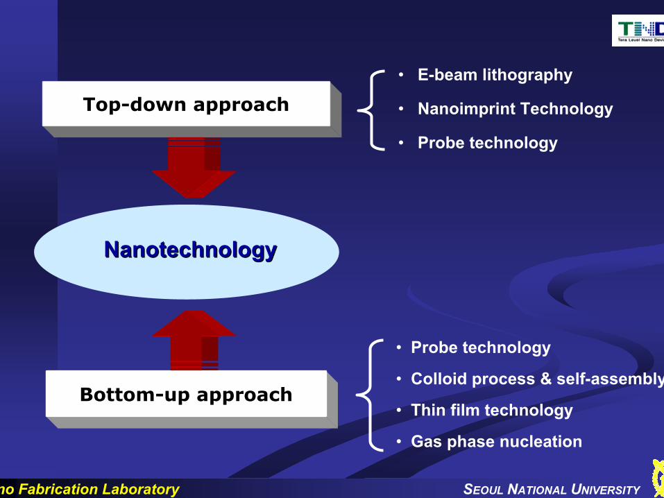
The essence of nanotechnology is the ability to work at the molecular level, atom by atom, to create large structures with fundamentally new molecular organization.
Nanotechnology is concerned with materials and systems whose structures and components exhibit novel and significantly improved physical, chemical, and biological properties, phenomena, and processes due to their nanoscale size.
Nanotechnology;Nanotechnology;

Nano Fabrication Laboratory SEOUL NATIONAL UNIVERSITY
~ nm
Å unit
2-D
1-D
0-D
3-D Bulk1022 ~ 1023 #/cm3
~ nmAtom
Nanotechnology
Nano Fabrication Laboratory SEOUL NATIONAL UNIVERSITY
Top-down approach
Bottom-up approach
NanotechnologyNanotechnology
• E-beam lithography
• Nanoimprint Technology
• Probe technology
• Colloid process & self-assembly
• Thin film technology
• Probe technology
• Gas phase nucleation
Nano Fabrication Laboratory SEOUL NATIONAL UNIVERSITY
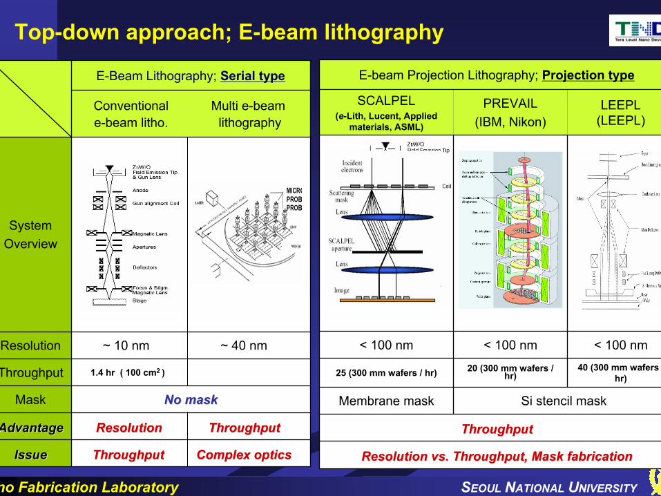
E-Beam Lithography; Serial type
SystemOverview
No maskNo maskMask
Resolution Throughput Resolution Throughput AdvantageAdvantage
Throughput Complex opticsThroughput Complex opticsIssueIssue
1.4 hr ( 100 cm2 )Throughput
~ 10 nm ~ 40 nmResolution
Top-down approach; E-beam lithography
Si stencil maskMembrane mask
ThroughputThroughput
Resolution vs. Throughput, Mask fabricationResolution vs. Throughput, Mask fabrication
LEEPL(LEEPL)
E-beam Projection Lithography; Projection type
PREVAIL(IBM, Nikon)
40 (300 mm wafers / hr)
20 (300 mm wafers / hr)25 (300 mm wafers / hr)
< 100 nm< 100 nm< 100 nm
SCALPEL(e-Lith, Lucent, Applied
materials, ASML)
Conventionale-beam litho.
Multi e-beamlithography
Nano Fabrication Laboratory SEOUL NATIONAL UNIVERSITY
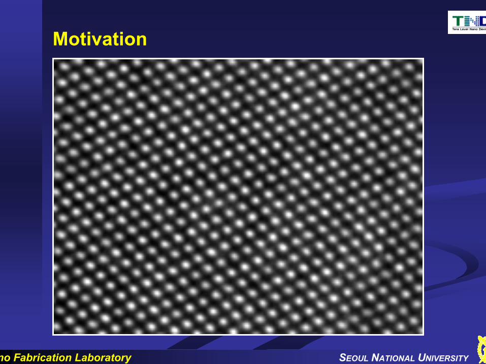
Motivation

Nano Fabrication Laboratory SEOUL NATIONAL UNIVERSITY
AIPEL (Atomic Image Projection E-beam Lithography)
- [Patent] Method for Forming a Pattern and a Semiconductor Device, Domestic(2001-1422), PCT (PCT/KR02/00043), Japan(2002-556925), EPO(2729593)application and USA (6767771 B2) registration
- [Patent] An Apparatus and a Method for Forming a pattern Using a Crystal Structure of Material, Domestic(2001-0017694), PCT(PCT/KR02/00109),Japan(2002-580390),EPO(2716458) application and USA registration (2004)
Wafer Stage
AIPEL MaskIncident electronSpecimen
Objective lens
Image Plane
Intermediate lens

Nano Fabrication Laboratory SEOUL NATIONAL UNIVERSITY
TEM Resolution from the Past
& 1956, Menter, first observed lattice image
(High Resolution)
1986, Ruska, Nobel prize winner
1931, Ruska & Knoll, Invented TEM
1936, 1st Commercial TEM (Siemens, Germany)
1961, Howie & Whelan,
Kinematical diffraction theory
1926, Schrodinger, Schrodinger equation
1928, Bethe, Dynamical diffraction theory
1939, Mollenstedt, CBED theory

Nano Fabrication Laboratory SEOUL NATIONAL UNIVERSITY
Sketch by Ruska of the cathod-ray tube for testing the one-stage and two-stage electron-optical imaging by means of two magnetic electron lenses ( 9 March 1931 )
Total magnification; 3.6 X 4.8 = 17.4
Accelerating voltage; 50kV
The first electron microscope, Ernst Ruska (1931)

Nano Fabrication Laboratory SEOUL NATIONAL UNIVERSITY
There’s Plenty of Room at the Bottom
December 29th 1959 at the annual meeting of the American Physical Society at the California Institute of Technology
An invitation to enter a new field of physics
• How do we write small ?
• Information on a small scale
• Better electron microscopes
• The marvelous biological system
• Miniaturizing the computer
• Miniaturization by evaporation
• Problems of lubrication
• A hundred tiny hands
• Rearranging the atoms
• Atoms in a small world
• High school competition Richard P. Feynman

Nano Fabrication Laboratory SEOUL NATIONAL UNIVERSITY
The next question is: How do we write it? We have no standard technique to do this now. But let me argue that it is not as difficult as it first appears to be. We can reverse the lenses of the electron microscope in order to demagnify as well as magnify. A source of ions, sent through the microscope lenses in reverse, could be focused to a very small spot. We could write with that spot like we write in a TV cathode ray oscilloscope, by going across in lines, and having an adjustment which determines the amount of material which is going to be deposited as we scan in lines.
This method might be very slow because of space charge limitations. There will be more rapid methods. We could first make, perhaps by some photo process, a screen which has holes in it in the form of the letters. Then we would strike an arc behind the holes and draw metallic ions through the holes; then we could again use our system of lenses and make a small image in the form of ions, which would deposit the metal on the pin.
A simple way might be this (though I am not sure it would work): We take light and, through an optical microscope running backwards, we focus it onto a very small photoelectric screen. Then electrons come away from the screen where the light is shinning. These electrons are focused down in size by the electron microscope lenses to impinge directly upon the surface of the metal. Will such a beam etch away the metal if it is run long enough? I don't know. If it doesn't work for a metal surface, it must be possible to find some surface with which to coat the original pin so that, where the electrons bombard, a change is made which we could recognize later.
How do we write small?

Nano Fabrication Laboratory SEOUL NATIONAL UNIVERSITY
AIPEL Hardware
Specifications– Accelerating voltage : 200 kV
– Electron gun type : Field emission gun
– Point-to-point resolution : 0.23 nm, Lattice resolution : 0.1 nm
– Patterning magnification : x20 ~ x300
– Lens system
OL – IL1 – PL1 – OL2 – IL2 – PL2
– Wafer stage where resist coated wafer can be inserted
A-stage : 4 mm x17 mm wafer
B-stage : 25 mm x 25 mm wafer
Wafer stage

Nano Fabrication Laboratory SEOUL NATIONAL UNIVERSITY
Modification of JEOL 2010F TEM
2010F AIPEL
LENS & STAGE modification
Objective lensObjective mini-lens
Patterning lenses
Intermediate lens 1
Intermediate lens 2 2nd objective lens
Wafer stage

Nano Fabrication Laboratory SEOUL NATIONAL UNIVERSITY
Sample (Natural mask)OL1IL1
PL1
OL2
IL2
PL2
Screen
Lithography stage
AIPEL hardware Ray diagram

Nano Fabrication Laboratory SEOUL NATIONAL UNIVERSITY
Modification of JEOL 2010F TEM
Modifications– Objective lens : Objective lens for 300 kV
– Patterning lens 1 & 2
: New lenses for generating patterns at the stage
: Magnification of objective lens and patterning lenses system : ×20 ~ ×300
– Wafer stage
: Two types of stages : 4×17 mm2 wafer stage(A-stage) and 25×25 mm2 wafer stage(B-stage)
– 2nd objective lens
Objective lens
Patterning lens
A-stage &2nd objective lens
Nano Fabrication Laboratory SEOUL NATIONAL UNIVERSITY
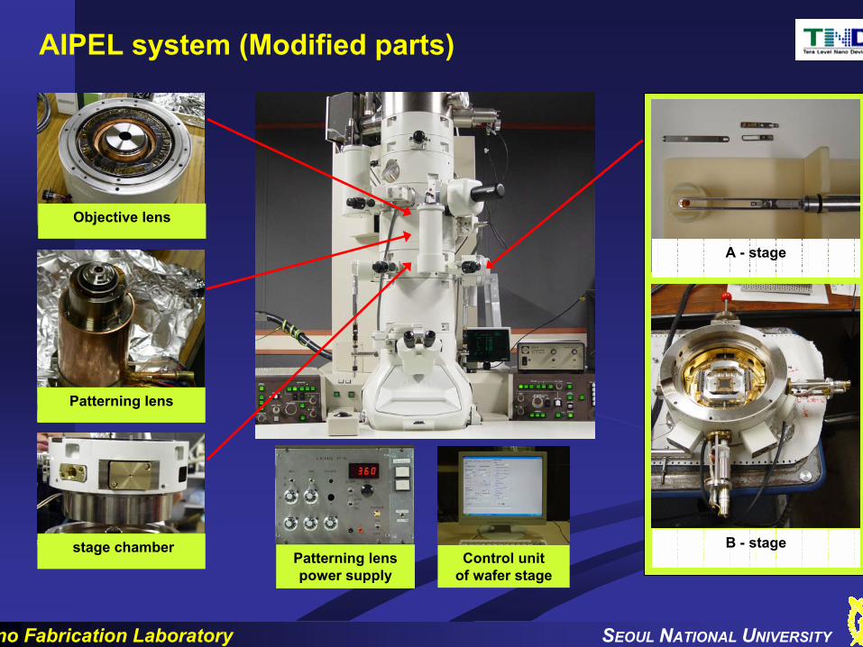
AIPEL system (Modified parts)
Objective lens
Patterning lens
stage chamber
A - stage
B - stage Patterning lens power supply
Control unit of wafer stage
Nano Fabrication Laboratory SEOUL NATIONAL UNIVERSITY
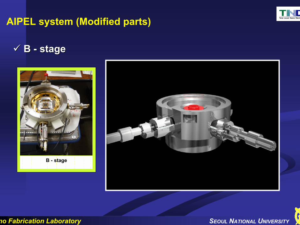
B - stage
AIPEL system (Modified parts)
B B -- stagestage

Nano Fabrication Laboratory SEOUL NATIONAL UNIVERSITY
Collaboration with JEOL in JAPANCollaboration with JEOL in JAPAN
Mr. Kim
“Hi, I am an AIPEL
team leader of
NFL.”
Dr. Arai
“Hello, I am a principal researcher of JEOL.”

Nano Fabrication Laboratory SEOUL NATIONAL UNIVERSITY
3-stage image forming system
– consists of OBJECTIVE(OL), INTERMEDIATE(IL), PROJECTOR LENS(PL)
AIPEL lens system
– consists of two 3-stage image forming systems
– Mask stage-OL-IL1-PL1-wafer stage-OL2-IL2-PL2
OL IL1 PL1 OL2 IL2 PL2
60 71 91 110 62 435 mm
fOL=2.3
(S+D)=306336 TMax.1500 AT
(S+D)=127080 TMax.3000 AT f2nd OL=5
(S+D)=13.53190 TMax.5200 AT
(S+D)=73190 TMax.5200 AT
TEM1TEM2
AIPEL lens systemAIPEL lens system

Nano Fabrication Laboratory SEOUL NATIONAL UNIVERSITY
Magnetic LensNewton’s Lens Equation
1 1 1a b f
bMa
+ =
=
1 10 100 10000.1
1
10
100
S/D=0.5 S/D=1.0 S/D=1.5 S/D=2.0
Circle : projector lensTriangle : objective lens
f/(S+
D)
(Ni)2/U*
2 *
25( ) ( ) /f
S D Ni U=
+
2 *2 *
25 0.0125 ( ) /( ) ( ) /f Ni U
S D Ni U= +
+
S: pole-piece gapD : bore diameterNi : ampere turnsU* : relativistic accelerating voltage
AIPEL lens systemAIPEL lens system
a b
f

Nano Fabrication Laboratory SEOUL NATIONAL UNIVERSITY
Magnification of AIPEL hardwareMagnification of AIPEL hardware
50 100 150 200 250 3000.0
0.1
0.2
0.3
0.4
0.5
Lens
Cur
rent
(A)
Patterning Magnification (times)
IL1 PL1
Fig.(a) Total magnification of AIPEL hardware as a function of the excitation of IL2
Fig. (b) Patterning magnification of AIPEL hardware as a function of the excitation of IL1 and PL1

Nano Fabrication Laboratory SEOUL NATIONAL UNIVERSITY
2
' ;'
SS
o
MMM S S δδ αα α
= = =
In TEM,
M=100,000 times, αo = 10 mrad, δs = 0.3 nm
Depth-of-focus (S) = 300 m
In AIPEL,
<Swafer
Resist coated wafer
δS : resolutionαo : beam semi-convergence angleM : magnification
DepthDepth--ofof--focus at wafer stagefocus at wafer stage

Nano Fabrication Laboratory SEOUL NATIONAL UNIVERSITY
50 100 150 200 250 3000.0
0.5
1.0
1.5
2.0
2.5
3.0
3.5
4.0
4.5
Patterning magnification (times)
D
epth
-of-f
ocus
(mm
)
Patterning condition for HSQ Patterning condition for ZEP520A
DepthDepth--ofof--focus at wafer stagefocus at wafer stage
Nano Fabrication Laboratory SEOUL NATIONAL UNIVERSITY
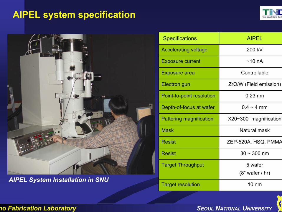
AIPEL system specification
AIPEL System Installation in SNU
0.23 nmPoint-to-point resolution
0.4 ~ 4 mmDepth-of-focus at wafer
10 nmTarget resolution
5 wafer(8” wafer / hr)
Target Throughput
30 ~ 300 nmResist
ZEP-520A, HSQ, PMMAResist
Natural maskMask
X20~300 magnificationPattering magnification
ZrO/W (Field emission)Electron gun
ControllableExposure area
~10 nAExposure current
200 kVAccelerating voltage
AIPELSpecifications
Nano Fabrication Laboratory SEOUL NATIONAL UNIVERSITY
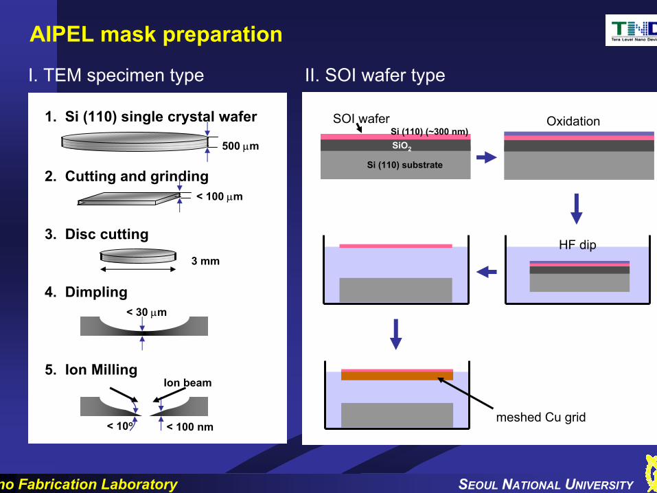
AIPEL mask preparation
1. Si (110) single crystal wafer
2. Cutting and grinding
3. Disc cutting
4. Dimpling< 30 µm
500 µm
< 100 µm
3 mm
5. Ion Milling
< 100 nm< 10o
Ion beam
Oxidation
HF dip
meshed Cu grid
Si (110) (~300 nm)SiO2
Si (110) substrate
SOI wafer
I. TEM specimen type II. SOI wafer type

Nano Fabrication Laboratory SEOUL NATIONAL UNIVERSITY
Electron signal from AIPEL mask
25.0MTFminmax
minmax
minmax
minmax =+−
=+−
=DDDD
IIII
Dmax
Dmin
P
Dexposure
minminmax 12cos
2Dx
PDDD +
+
−=
π
exposuremin
exposuremax
D.DD.D
×=
×=
81903661
When MTF is 0.25,
Dose distribution modeling

Nano Fabrication Laboratory SEOUL NATIONAL UNIVERSITY
AIPEL patterning ; Experimental condition
– Mask : Si single crystal
– Beam current : 3.3 nA
– Patterning magnification : x100 ~ x200
– Resist : 100 nm-thick-HSQ (Hydrogen silsesquioxane)
– Exposure conditions :
Dose : 1000 ~ 1700 µC/cm2, Exposure time : 1.0 ~ 1.5 sec
– Development condition;
TMAH 25% (in water) 60 sec, D.I. water rinse 120 sec
Nano Fabrication Laboratory SEOUL NATIONAL UNIVERSITY
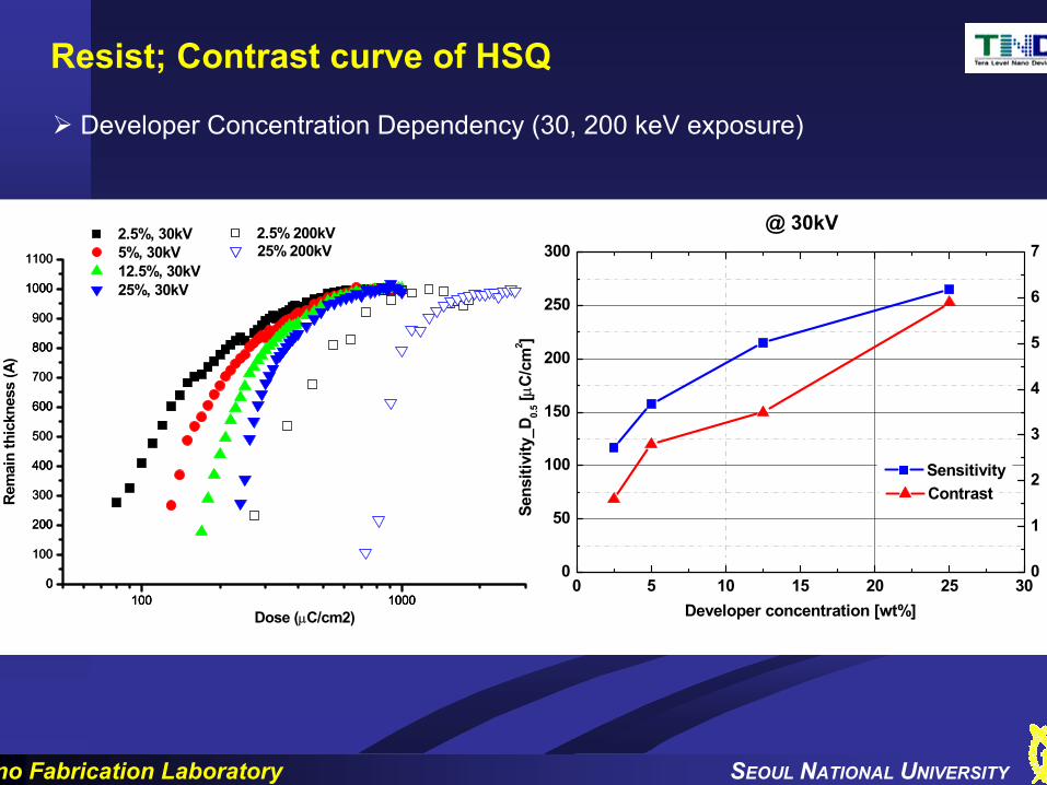
Resist; Contrast curve of HSQ
Developer Concentration Dependency (30, 200 keV exposure)
0
50
100
150
200
250
300
0 5 10 15 20 25 300
1
2
3
4
5
6
7
Sens
itivi
ty_D
0.5 [µC
/cm
2 ]
Sensitivity
Developer concentration [wt%]
Cont
rast
Contrast
100 10000
100
200
300
400
500
600
700
800
900
1000
1100
100 10000
100
200
300
400
500
600
700
800
900
1000
1100
100 10000
200
400
600
800
1000
Rem
ain
thic
knes
s (A
)
Dose (µC/cm2)
2.5%, 30kV 5%, 30kV 12.5%, 30kV 25%, 30kV
2.5% 200kV 25% 200kV
@ 30kV

Nano Fabrication Laboratory SEOUL NATIONAL UNIVERSITY
AIPEL patterning ; Experimental results (HSQ)
Pattern image on resistDot patterns: 180Dot patterns: 180xx, Pitch 65nm, Pitch 65nm
Resist : HSQ,
Dose : 1039 µC/cm2,
Exposure time : 1.2 sec
2 nm
Mask image
180X

Nano Fabrication Laboratory SEOUL NATIONAL UNIVERSITY
Resist : HSQ,
Dose : 1263 µC/cm2,
Exposure time : 1.5 sec
AIPEL patterning ; Experimental results (HSQ)Dot patterns: 160Dot patterns: 160xx, Pitch 55nm, Pitch 55nm
Pattern image on resist
2 nm
Mask image
160X
Nano Fabrication Laboratory SEOUL NATIONAL UNIVERSITY
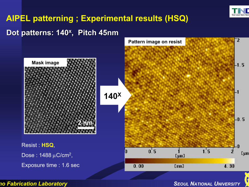
AIPEL patterning ; Experimental results (HSQ)Dot patterns: 140Dot patterns: 140xx, Pitch 45nm, Pitch 45nm
Pattern image on resist
Resist : HSQ,
Dose : 1488 µC/cm2,
Exposure time : 1.6 sec
2 nm
Mask image
140X

Nano Fabrication Laboratory SEOUL NATIONAL UNIVERSITY
AIPEL patterning ; Experimental results (HSQ)Dot patterns: 120Dot patterns: 120xx, Pitch 40nm, Pitch 40nm
Pattern image on resist
Resist : HSQ,
Dose : 1416 µC/cm2,
Exposure time : 1.5 sec
2 nm
Mask image
120X

Nano Fabrication Laboratory SEOUL NATIONAL UNIVERSITY
AIPEL patterning ; Experimental results (HSQ)Dot patterns: 100Dot patterns: 100xx, Pitch 35nm, Pitch 35nm
Resist : HSQ,
Dose : 1260 µC/cm2,
Exposure time : 1.5 sec
2 nm
Mask image
Pattern image on resist
100X

Nano Fabrication Laboratory SEOUL NATIONAL UNIVERSITY
AIPEL patterning ; Experimental results (Si3N4 mask)Line patterns: 160Line patterns: 160xx, Pitch 105nm, Pitch 105nm
Resist : HSQ, Dose : 1260 µC/cm2, Exposure time : 1.5 sec
10nm
Mask image Pattern image on resist
160X

Nano Fabrication Laboratory SEOUL NATIONAL UNIVERSITY
AIPEL patterning ; Experimental results (Si3N4 mask)Line patterns: 120Line patterns: 120xx, Pitch 90nm, Pitch 90nm
Resist : HSQ, Dose : 1260 µC/cm2, Exposure time : 1.5 sec
10nm
Mask image
120X
Pattern image on resist

Nano Fabrication Laboratory SEOUL NATIONAL UNIVERSITY
AIPEL patterning ; Experimental results (Si3N4 mask)Line patterns: 100Line patterns: 100xx, Pitch 70nm, Pitch 70nm
Resist : HSQ, Dose : 1260 µC/cm2, Exposure time : 1.5 sec
10nm
Mask image
100X
Pattern image on resist

Nano Fabrication Laboratory SEOUL NATIONAL UNIVERSITY
Complicate (6Complicate (6--fold symmetry) patterns: 160fold symmetry) patterns: 160x x (HSQ)(HSQ)
AIPEL patterning ; Experimental results (Si3N4 mask)
Pattern image on resist
Resist : HSQ, Dose : 1260 µC/cm2, Exposure time : 1.5 sec
2 nm
Mask image
160X

Nano Fabrication Laboratory SEOUL NATIONAL UNIVERSITY
AIPEL Simulation

Nano Fabrication Laboratory SEOUL NATIONAL UNIVERSITY
ELIS simulator

Nano Fabrication Laboratory SEOUL NATIONAL UNIVERSITY
Simulation results
Mag. X300
ZEP520A
Mask image Experimental resultsSimulation results
Mask image
Mag. X300
ZEP520A
Experimental resultsSimulation results

Nano Fabrication Laboratory SEOUL NATIONAL UNIVERSITY
Patterns from Nature

Nano Fabrication Laboratory SEOUL NATIONAL UNIVERSITY
The First Electron Microscope, Ruska (1931)The First Flight, Wright brothers (1903)
Flight time ; 12 secFlight distance ; 36 m
Magnification ; X 17.5Accelerating voltage ; 50 kV
Nano Fabrication Laboratory SEOUL NATIONAL UNIVERSITY
Acknowledgement
TeraTera--Level Level NanoelectronicsNanoelectronics Program (Dr. JoProgram (Dr. Jo--Won Lee)Won Lee)
NanoNano Fabrication Laboratory at SNU: Fabrication Laboratory at SNU:
ByungByung--Sung Kim (Ph.D. AIPEL project initiation) Sung Kim (Ph.D. AIPEL project initiation)
HyunHyun--Mi Kim (Post doc. New mask process) Mi Kim (Post doc. New mask process)
HyoHyo--Sung Lee (AIPEL process improvement) Sung Lee (AIPEL process improvement)
JungJung--Sub Yi (Mix and match process) Sub Yi (Mix and match process)
KyungKyung--BaeBae Jin (Etch process)Jin (Etch process)
ElecronElecron--Beam Lithography Simulation at SNU:Beam Lithography Simulation at SNU:
Prof. Prof. KukKuk--Jin JunJin Jun
KRISS (Dr. YangKRISS (Dr. Yang--KooKoo ChoCho): Stage Design): Stage Design
JEOL. Ltd.; Yoshihiro Arai JEOL. Ltd.; Yoshihiro Arai